EP2750212B1 - Light emitting device package, light emitting device using that package, and illumination device using the light emitting devices - Google Patents
Light emitting device package, light emitting device using that package, and illumination device using the light emitting devices Download PDFInfo
- Publication number
- EP2750212B1 EP2750212B1 EP13199676.1A EP13199676A EP2750212B1 EP 2750212 B1 EP2750212 B1 EP 2750212B1 EP 13199676 A EP13199676 A EP 13199676A EP 2750212 B1 EP2750212 B1 EP 2750212B1
- Authority
- EP
- European Patent Office
- Prior art keywords
- lead
- light emitting
- frame
- emitting device
- package
- Prior art date
- Legal status (The legal status is an assumption and is not a legal conclusion. Google has not performed a legal analysis and makes no representation as to the accuracy of the status listed.)
- Active
Links
- 238000005286 illumination Methods 0.000 title claims description 20
- 229920005989 resin Polymers 0.000 claims description 96
- 239000011347 resin Substances 0.000 claims description 96
- 238000005192 partition Methods 0.000 claims description 30
- 239000000463 material Substances 0.000 description 69
- 239000000853 adhesive Substances 0.000 description 24
- 230000001070 adhesive effect Effects 0.000 description 24
- 229910052751 metal Inorganic materials 0.000 description 22
- 239000002184 metal Substances 0.000 description 22
- 238000000605 extraction Methods 0.000 description 14
- 230000009467 reduction Effects 0.000 description 13
- 239000000758 substrate Substances 0.000 description 12
- BQCADISMDOOEFD-UHFFFAOYSA-N Silver Chemical compound [Ag] BQCADISMDOOEFD-UHFFFAOYSA-N 0.000 description 10
- 229910052709 silver Inorganic materials 0.000 description 10
- 239000004332 silver Substances 0.000 description 10
- 229910052784 alkaline earth metal Inorganic materials 0.000 description 7
- 150000002739 metals Chemical class 0.000 description 7
- VYPSYNLAJGMNEJ-UHFFFAOYSA-N Silicium dioxide Chemical compound O=[Si]=O VYPSYNLAJGMNEJ-UHFFFAOYSA-N 0.000 description 6
- 229910052782 aluminium Inorganic materials 0.000 description 6
- XAGFODPZIPBFFR-UHFFFAOYSA-N aluminium Chemical compound [Al] XAGFODPZIPBFFR-UHFFFAOYSA-N 0.000 description 6
- 238000009826 distribution Methods 0.000 description 6
- 239000000945 filler Substances 0.000 description 6
- PCHJSUWPFVWCPO-UHFFFAOYSA-N gold Chemical compound [Au] PCHJSUWPFVWCPO-UHFFFAOYSA-N 0.000 description 6
- 229910052737 gold Inorganic materials 0.000 description 6
- 239000010931 gold Substances 0.000 description 6
- -1 polyethylene terephthalate Polymers 0.000 description 6
- 239000004065 semiconductor Substances 0.000 description 6
- RYGMFSIKBFXOCR-UHFFFAOYSA-N Copper Chemical compound [Cu] RYGMFSIKBFXOCR-UHFFFAOYSA-N 0.000 description 5
- 229910052802 copper Inorganic materials 0.000 description 5
- 239000010949 copper Substances 0.000 description 5
- 229920002050 silicone resin Polymers 0.000 description 5
- VTYYLEPIZMXCLO-UHFFFAOYSA-L Calcium carbonate Chemical compound [Ca+2].[O-]C([O-])=O VTYYLEPIZMXCLO-UHFFFAOYSA-L 0.000 description 4
- 229910052693 Europium Inorganic materials 0.000 description 4
- XEEYBQQBJWHFJM-UHFFFAOYSA-N Iron Chemical compound [Fe] XEEYBQQBJWHFJM-UHFFFAOYSA-N 0.000 description 4
- UQSXHKLRYXJYBZ-UHFFFAOYSA-N Iron oxide Chemical compound [Fe]=O UQSXHKLRYXJYBZ-UHFFFAOYSA-N 0.000 description 4
- PXHVJJICTQNCMI-UHFFFAOYSA-N Nickel Chemical compound [Ni] PXHVJJICTQNCMI-UHFFFAOYSA-N 0.000 description 4
- XLOMVQKBTHCTTD-UHFFFAOYSA-N Zinc monoxide Chemical compound [Zn]=O XLOMVQKBTHCTTD-UHFFFAOYSA-N 0.000 description 4
- 150000001342 alkaline earth metals Chemical class 0.000 description 4
- 229910045601 alloy Inorganic materials 0.000 description 4
- 239000000956 alloy Substances 0.000 description 4
- OGPBJKLSAFTDLK-UHFFFAOYSA-N europium atom Chemical compound [Eu] OGPBJKLSAFTDLK-UHFFFAOYSA-N 0.000 description 4
- AMWRITDGCCNYAT-UHFFFAOYSA-L hydroxy(oxo)manganese;manganese Chemical compound [Mn].O[Mn]=O.O[Mn]=O AMWRITDGCCNYAT-UHFFFAOYSA-L 0.000 description 4
- 238000000465 moulding Methods 0.000 description 4
- 150000004767 nitrides Chemical class 0.000 description 4
- 238000000926 separation method Methods 0.000 description 4
- 229910052684 Cerium Inorganic materials 0.000 description 3
- GWEVSGVZZGPLCZ-UHFFFAOYSA-N Titan oxide Chemical compound O=[Ti]=O GWEVSGVZZGPLCZ-UHFFFAOYSA-N 0.000 description 3
- 238000005452 bending Methods 0.000 description 3
- 239000003822 epoxy resin Substances 0.000 description 3
- 239000011521 glass Substances 0.000 description 3
- 238000002955 isolation Methods 0.000 description 3
- TWNQGVIAIRXVLR-UHFFFAOYSA-N oxo(oxoalumanyloxy)alumane Chemical compound O=[Al]O[Al]=O TWNQGVIAIRXVLR-UHFFFAOYSA-N 0.000 description 3
- 229920000647 polyepoxide Polymers 0.000 description 3
- 229910052761 rare earth metal Inorganic materials 0.000 description 3
- 239000000377 silicon dioxide Substances 0.000 description 3
- OGIDPMRJRNCKJF-UHFFFAOYSA-N titanium oxide Inorganic materials [Ti]=O OGIDPMRJRNCKJF-UHFFFAOYSA-N 0.000 description 3
- KDLHZDBZIXYQEI-UHFFFAOYSA-N Palladium Chemical compound [Pd] KDLHZDBZIXYQEI-UHFFFAOYSA-N 0.000 description 2
- 229910000831 Steel Inorganic materials 0.000 description 2
- 229910052915 alkaline earth metal silicate Inorganic materials 0.000 description 2
- 229910002113 barium titanate Inorganic materials 0.000 description 2
- JRPBQTZRNDNNOP-UHFFFAOYSA-N barium titanate Chemical compound [Ba+2].[Ba+2].[O-][Ti]([O-])([O-])[O-] JRPBQTZRNDNNOP-UHFFFAOYSA-N 0.000 description 2
- 229910000019 calcium carbonate Inorganic materials 0.000 description 2
- AXCZMVOFGPJBDE-UHFFFAOYSA-L calcium dihydroxide Chemical compound [OH-].[OH-].[Ca+2] AXCZMVOFGPJBDE-UHFFFAOYSA-L 0.000 description 2
- 239000000920 calcium hydroxide Substances 0.000 description 2
- 229910001861 calcium hydroxide Inorganic materials 0.000 description 2
- 239000000378 calcium silicate Substances 0.000 description 2
- 229910052918 calcium silicate Inorganic materials 0.000 description 2
- OYACROKNLOSFPA-UHFFFAOYSA-N calcium;dioxido(oxo)silane Chemical compound [Ca+2].[O-][Si]([O-])=O OYACROKNLOSFPA-UHFFFAOYSA-N 0.000 description 2
- 239000006229 carbon black Substances 0.000 description 2
- GWXLDORMOJMVQZ-UHFFFAOYSA-N cerium Chemical compound [Ce] GWXLDORMOJMVQZ-UHFFFAOYSA-N 0.000 description 2
- KUNSUQLRTQLHQQ-UHFFFAOYSA-N copper tin Chemical compound [Cu].[Sn] KUNSUQLRTQLHQQ-UHFFFAOYSA-N 0.000 description 2
- 230000032798 delamination Effects 0.000 description 2
- QDOXWKRWXJOMAK-UHFFFAOYSA-N dichromium trioxide Chemical compound O=[Cr]O[Cr]=O QDOXWKRWXJOMAK-UHFFFAOYSA-N 0.000 description 2
- 230000000694 effects Effects 0.000 description 2
- 230000005611 electricity Effects 0.000 description 2
- 238000005530 etching Methods 0.000 description 2
- 239000000835 fiber Substances 0.000 description 2
- 238000011049 filling Methods 0.000 description 2
- 229910052742 iron Inorganic materials 0.000 description 2
- ZLNQQNXFFQJAID-UHFFFAOYSA-L magnesium carbonate Chemical compound [Mg+2].[O-]C([O-])=O ZLNQQNXFFQJAID-UHFFFAOYSA-L 0.000 description 2
- 239000001095 magnesium carbonate Substances 0.000 description 2
- 229910000021 magnesium carbonate Inorganic materials 0.000 description 2
- VTHJTEIRLNZDEV-UHFFFAOYSA-L magnesium dihydroxide Chemical compound [OH-].[OH-].[Mg+2] VTHJTEIRLNZDEV-UHFFFAOYSA-L 0.000 description 2
- 239000000347 magnesium hydroxide Substances 0.000 description 2
- 229910001862 magnesium hydroxide Inorganic materials 0.000 description 2
- 239000000395 magnesium oxide Substances 0.000 description 2
- CPLXHLVBOLITMK-UHFFFAOYSA-N magnesium oxide Inorganic materials [Mg]=O CPLXHLVBOLITMK-UHFFFAOYSA-N 0.000 description 2
- AXZKOIWUVFPNLO-UHFFFAOYSA-N magnesium;oxygen(2-) Chemical compound [O-2].[Mg+2] AXZKOIWUVFPNLO-UHFFFAOYSA-N 0.000 description 2
- 229910052759 nickel Inorganic materials 0.000 description 2
- 239000002245 particle Substances 0.000 description 2
- 239000000049 pigment Substances 0.000 description 2
- BASFCYQUMIYNBI-UHFFFAOYSA-N platinum Chemical compound [Pt] BASFCYQUMIYNBI-UHFFFAOYSA-N 0.000 description 2
- 229920005668 polycarbonate resin Polymers 0.000 description 2
- 239000004431 polycarbonate resin Substances 0.000 description 2
- 229920001721 polyimide Polymers 0.000 description 2
- 239000009719 polyimide resin Substances 0.000 description 2
- 229920001296 polysiloxane Polymers 0.000 description 2
- 239000010959 steel Substances 0.000 description 2
- 239000000126 substance Substances 0.000 description 2
- WFKWXMTUELFFGS-UHFFFAOYSA-N tungsten Chemical compound [W] WFKWXMTUELFFGS-UHFFFAOYSA-N 0.000 description 2
- 229910052721 tungsten Inorganic materials 0.000 description 2
- 239000010937 tungsten Substances 0.000 description 2
- 239000011787 zinc oxide Substances 0.000 description 2
- 229920000178 Acrylic resin Polymers 0.000 description 1
- 239000004925 Acrylic resin Substances 0.000 description 1
- 239000004953 Aliphatic polyamide Substances 0.000 description 1
- JBRZTFJDHDCESZ-UHFFFAOYSA-N AsGa Chemical compound [As]#[Ga] JBRZTFJDHDCESZ-UHFFFAOYSA-N 0.000 description 1
- BTBUEUYNUDRHOZ-UHFFFAOYSA-N Borate Chemical compound [O-]B([O-])[O-] BTBUEUYNUDRHOZ-UHFFFAOYSA-N 0.000 description 1
- 229910000906 Bronze Inorganic materials 0.000 description 1
- VYZAMTAEIAYCRO-UHFFFAOYSA-N Chromium Chemical compound [Cr] VYZAMTAEIAYCRO-UHFFFAOYSA-N 0.000 description 1
- 229910000881 Cu alloy Inorganic materials 0.000 description 1
- 239000004593 Epoxy Substances 0.000 description 1
- 229910000640 Fe alloy Inorganic materials 0.000 description 1
- 229910005540 GaP Inorganic materials 0.000 description 1
- 229910001218 Gallium arsenide Inorganic materials 0.000 description 1
- 229920000106 Liquid crystal polymer Polymers 0.000 description 1
- 239000004977 Liquid-crystal polymers (LCPs) Substances 0.000 description 1
- ZOKXTWBITQBERF-UHFFFAOYSA-N Molybdenum Chemical compound [Mo] ZOKXTWBITQBERF-UHFFFAOYSA-N 0.000 description 1
- BPQQTUXANYXVAA-UHFFFAOYSA-N Orthosilicate Chemical compound [O-][Si]([O-])([O-])[O-] BPQQTUXANYXVAA-UHFFFAOYSA-N 0.000 description 1
- OAICVXFJPJFONN-UHFFFAOYSA-N Phosphorus Chemical compound [P] OAICVXFJPJFONN-UHFFFAOYSA-N 0.000 description 1
- 239000004695 Polyether sulfone Substances 0.000 description 1
- 239000004734 Polyphenylene sulfide Substances 0.000 description 1
- 229910052581 Si3N4 Inorganic materials 0.000 description 1
- 229920010524 Syndiotactic polystyrene Polymers 0.000 description 1
- RTAQQCXQSZGOHL-UHFFFAOYSA-N Titanium Chemical compound [Ti] RTAQQCXQSZGOHL-UHFFFAOYSA-N 0.000 description 1
- QCEUXSAXTBNJGO-UHFFFAOYSA-N [Ag].[Sn] Chemical compound [Ag].[Sn] QCEUXSAXTBNJGO-UHFFFAOYSA-N 0.000 description 1
- 229920003231 aliphatic polyamide Polymers 0.000 description 1
- 150000004645 aluminates Chemical class 0.000 description 1
- PNEYBMLMFCGWSK-UHFFFAOYSA-N aluminium oxide Inorganic materials [O-2].[O-2].[O-2].[Al+3].[Al+3] PNEYBMLMFCGWSK-UHFFFAOYSA-N 0.000 description 1
- OJMOMXZKOWKUTA-UHFFFAOYSA-N aluminum;borate Chemical compound [Al+3].[O-]B([O-])[O-] OJMOMXZKOWKUTA-UHFFFAOYSA-N 0.000 description 1
- 229910000410 antimony oxide Inorganic materials 0.000 description 1
- 229910052586 apatite Inorganic materials 0.000 description 1
- 230000008901 benefit Effects 0.000 description 1
- JWVAUCBYEDDGAD-UHFFFAOYSA-N bismuth tin Chemical compound [Sn].[Bi] JWVAUCBYEDDGAD-UHFFFAOYSA-N 0.000 description 1
- 239000010974 bronze Substances 0.000 description 1
- AOWKSNWVBZGMTJ-UHFFFAOYSA-N calcium titanate Chemical compound [Ca+2].[O-][Ti]([O-])=O AOWKSNWVBZGMTJ-UHFFFAOYSA-N 0.000 description 1
- 239000000919 ceramic Substances 0.000 description 1
- 229910019990 cerium-doped yttrium aluminum garnet Inorganic materials 0.000 description 1
- 229910017052 cobalt Inorganic materials 0.000 description 1
- 239000010941 cobalt Substances 0.000 description 1
- GUTLYIVDDKVIGB-UHFFFAOYSA-N cobalt atom Chemical compound [Co] GUTLYIVDDKVIGB-UHFFFAOYSA-N 0.000 description 1
- 239000003086 colorant Substances 0.000 description 1
- 238000004040 coloring Methods 0.000 description 1
- 239000011365 complex material Substances 0.000 description 1
- 239000000470 constituent Substances 0.000 description 1
- IYRDVAUFQZOLSB-UHFFFAOYSA-N copper iron Chemical compound [Fe].[Cu] IYRDVAUFQZOLSB-UHFFFAOYSA-N 0.000 description 1
- PMHQVHHXPFUNSP-UHFFFAOYSA-M copper(1+);methylsulfanylmethane;bromide Chemical compound Br[Cu].CSC PMHQVHHXPFUNSP-UHFFFAOYSA-M 0.000 description 1
- 230000001419 dependent effect Effects 0.000 description 1
- 238000011038 discontinuous diafiltration by volume reduction Methods 0.000 description 1
- 239000002270 dispersing agent Substances 0.000 description 1
- 239000000428 dust Substances 0.000 description 1
- 238000005516 engineering process Methods 0.000 description 1
- 230000002349 favourable effect Effects 0.000 description 1
- 239000012530 fluid Substances 0.000 description 1
- 230000004907 flux Effects 0.000 description 1
- HZXMRANICFIONG-UHFFFAOYSA-N gallium phosphide Chemical compound [Ga]#P HZXMRANICFIONG-UHFFFAOYSA-N 0.000 description 1
- JVPLOXQKFGYFMN-UHFFFAOYSA-N gold tin Chemical compound [Sn].[Au] JVPLOXQKFGYFMN-UHFFFAOYSA-N 0.000 description 1
- 229910052736 halogen Inorganic materials 0.000 description 1
- 150000002367 halogens Chemical class 0.000 description 1
- 238000010438 heat treatment Methods 0.000 description 1
- 230000006872 improvement Effects 0.000 description 1
- 230000031700 light absorption Effects 0.000 description 1
- 239000007788 liquid Substances 0.000 description 1
- 239000004973 liquid crystal related substance Substances 0.000 description 1
- 238000011068 loading method Methods 0.000 description 1
- HCWCAKKEBCNQJP-UHFFFAOYSA-N magnesium orthosilicate Chemical compound [Mg+2].[Mg+2].[O-][Si]([O-])([O-])[O-] HCWCAKKEBCNQJP-UHFFFAOYSA-N 0.000 description 1
- 239000000391 magnesium silicate Substances 0.000 description 1
- 229910052919 magnesium silicate Inorganic materials 0.000 description 1
- 235000019792 magnesium silicate Nutrition 0.000 description 1
- WPBNNNQJVZRUHP-UHFFFAOYSA-L manganese(2+);methyl n-[[2-(methoxycarbonylcarbamothioylamino)phenyl]carbamothioyl]carbamate;n-[2-(sulfidocarbothioylamino)ethyl]carbamodithioate Chemical compound [Mn+2].[S-]C(=S)NCCNC([S-])=S.COC(=O)NC(=S)NC1=CC=CC=C1NC(=S)NC(=O)OC WPBNNNQJVZRUHP-UHFFFAOYSA-L 0.000 description 1
- 239000011159 matrix material Substances 0.000 description 1
- 239000007769 metal material Substances 0.000 description 1
- 238000000034 method Methods 0.000 description 1
- 239000010445 mica Substances 0.000 description 1
- 229910052618 mica group Inorganic materials 0.000 description 1
- 230000004048 modification Effects 0.000 description 1
- 238000012986 modification Methods 0.000 description 1
- 229910052750 molybdenum Inorganic materials 0.000 description 1
- 239000011733 molybdenum Substances 0.000 description 1
- VTRUBDSFZJNXHI-UHFFFAOYSA-N oxoantimony Chemical compound [Sb]=O VTRUBDSFZJNXHI-UHFFFAOYSA-N 0.000 description 1
- 229910052763 palladium Inorganic materials 0.000 description 1
- 239000005011 phenolic resin Substances 0.000 description 1
- 238000007747 plating Methods 0.000 description 1
- 229910052697 platinum Inorganic materials 0.000 description 1
- 229920001643 poly(ether ketone) Polymers 0.000 description 1
- 229920000636 poly(norbornene) polymer Polymers 0.000 description 1
- 229920001230 polyarylate Polymers 0.000 description 1
- 229920006393 polyether sulfone Polymers 0.000 description 1
- 229920000139 polyethylene terephthalate Polymers 0.000 description 1
- 239000005020 polyethylene terephthalate Substances 0.000 description 1
- 229920000306 polymethylpentene Polymers 0.000 description 1
- 239000011116 polymethylpentene Substances 0.000 description 1
- 229920001955 polyphenylene ether Polymers 0.000 description 1
- 229920000069 polyphenylene sulfide Polymers 0.000 description 1
- 229920005749 polyurethane resin Polymers 0.000 description 1
- 238000003825 pressing Methods 0.000 description 1
- 229910052703 rhodium Inorganic materials 0.000 description 1
- 239000010948 rhodium Substances 0.000 description 1
- MHOVAHRLVXNVSD-UHFFFAOYSA-N rhodium atom Chemical compound [Rh] MHOVAHRLVXNVSD-UHFFFAOYSA-N 0.000 description 1
- 238000005096 rolling process Methods 0.000 description 1
- 229910052594 sapphire Inorganic materials 0.000 description 1
- 239000010980 sapphire Substances 0.000 description 1
- 229920006012 semi-aromatic polyamide Polymers 0.000 description 1
- 150000004760 silicates Chemical class 0.000 description 1
- HBMJWWWQQXIZIP-UHFFFAOYSA-N silicon carbide Chemical compound [Si+]#[C-] HBMJWWWQQXIZIP-UHFFFAOYSA-N 0.000 description 1
- 229910010271 silicon carbide Inorganic materials 0.000 description 1
- 229910000679 solder Inorganic materials 0.000 description 1
- 239000007787 solid Substances 0.000 description 1
- 230000003068 static effect Effects 0.000 description 1
- KKEYFWRCBNTPAC-UHFFFAOYSA-L terephthalate(2-) Chemical compound [O-]C(=O)C1=CC=C(C([O-])=O)C=C1 KKEYFWRCBNTPAC-UHFFFAOYSA-L 0.000 description 1
- 229920005992 thermoplastic resin Polymers 0.000 description 1
- 229920001187 thermosetting polymer Polymers 0.000 description 1
- 239000010409 thin film Substances 0.000 description 1
- 229910052719 titanium Inorganic materials 0.000 description 1
- 239000010936 titanium Substances 0.000 description 1
- 150000003624 transition metals Chemical group 0.000 description 1
- BIKXLKXABVUSMH-UHFFFAOYSA-N trizinc;diborate Chemical compound [Zn+2].[Zn+2].[Zn+2].[O-]B([O-])[O-].[O-]B([O-])[O-] BIKXLKXABVUSMH-UHFFFAOYSA-N 0.000 description 1
- 239000010456 wollastonite Substances 0.000 description 1
- 229910052882 wollastonite Inorganic materials 0.000 description 1
- BNEMLSQAJOPTGK-UHFFFAOYSA-N zinc;dioxido(oxo)tin Chemical compound [Zn+2].[O-][Sn]([O-])=O BNEMLSQAJOPTGK-UHFFFAOYSA-N 0.000 description 1
Images

Classifications
-
- H—ELECTRICITY
- H01—ELECTRIC ELEMENTS
- H01L—SEMICONDUCTOR DEVICES NOT COVERED BY CLASS H10
- H01L25/00—Assemblies consisting of a plurality of individual semiconductor or other solid state devices ; Multistep manufacturing processes thereof
- H01L25/03—Assemblies consisting of a plurality of individual semiconductor or other solid state devices ; Multistep manufacturing processes thereof all the devices being of a type provided for in the same subgroup of groups H01L27/00 - H01L33/00, or in a single subclass of H10K, H10N, e.g. assemblies of rectifier diodes
- H01L25/10—Assemblies consisting of a plurality of individual semiconductor or other solid state devices ; Multistep manufacturing processes thereof all the devices being of a type provided for in the same subgroup of groups H01L27/00 - H01L33/00, or in a single subclass of H10K, H10N, e.g. assemblies of rectifier diodes the devices having separate containers
- H01L25/13—Assemblies consisting of a plurality of individual semiconductor or other solid state devices ; Multistep manufacturing processes thereof all the devices being of a type provided for in the same subgroup of groups H01L27/00 - H01L33/00, or in a single subclass of H10K, H10N, e.g. assemblies of rectifier diodes the devices having separate containers the devices being of a type provided for in group H01L33/00
-
- H—ELECTRICITY
- H01—ELECTRIC ELEMENTS
- H01L—SEMICONDUCTOR DEVICES NOT COVERED BY CLASS H10
- H01L23/00—Details of semiconductor or other solid state devices
- H01L23/48—Arrangements for conducting electric current to or from the solid state body in operation, e.g. leads, terminal arrangements ; Selection of materials therefor
- H01L23/488—Arrangements for conducting electric current to or from the solid state body in operation, e.g. leads, terminal arrangements ; Selection of materials therefor consisting of soldered or bonded constructions
- H01L23/495—Lead-frames or other flat leads
-
- H—ELECTRICITY
- H01—ELECTRIC ELEMENTS
- H01L—SEMICONDUCTOR DEVICES NOT COVERED BY CLASS H10
- H01L23/00—Details of semiconductor or other solid state devices
- H01L23/52—Arrangements for conducting electric current within the device in operation from one component to another, i.e. interconnections, e.g. wires, lead frames
- H01L23/522—Arrangements for conducting electric current within the device in operation from one component to another, i.e. interconnections, e.g. wires, lead frames including external interconnections consisting of a multilayer structure of conductive and insulating layers inseparably formed on the semiconductor body
- H01L23/528—Geometry or layout of the interconnection structure
- H01L23/5283—Cross-sectional geometry
-
- H—ELECTRICITY
- H01—ELECTRIC ELEMENTS
- H01L—SEMICONDUCTOR DEVICES NOT COVERED BY CLASS H10
- H01L25/00—Assemblies consisting of a plurality of individual semiconductor or other solid state devices ; Multistep manufacturing processes thereof
- H01L25/03—Assemblies consisting of a plurality of individual semiconductor or other solid state devices ; Multistep manufacturing processes thereof all the devices being of a type provided for in the same subgroup of groups H01L27/00 - H01L33/00, or in a single subclass of H10K, H10N, e.g. assemblies of rectifier diodes
- H01L25/04—Assemblies consisting of a plurality of individual semiconductor or other solid state devices ; Multistep manufacturing processes thereof all the devices being of a type provided for in the same subgroup of groups H01L27/00 - H01L33/00, or in a single subclass of H10K, H10N, e.g. assemblies of rectifier diodes the devices not having separate containers
- H01L25/075—Assemblies consisting of a plurality of individual semiconductor or other solid state devices ; Multistep manufacturing processes thereof all the devices being of a type provided for in the same subgroup of groups H01L27/00 - H01L33/00, or in a single subclass of H10K, H10N, e.g. assemblies of rectifier diodes the devices not having separate containers the devices being of a type provided for in group H01L33/00
-
- H—ELECTRICITY
- H01—ELECTRIC ELEMENTS
- H01L—SEMICONDUCTOR DEVICES NOT COVERED BY CLASS H10
- H01L28/00—Passive two-terminal components without a potential-jump or surface barrier for integrated circuits; Details thereof; Multistep manufacturing processes therefor
- H01L28/10—Inductors
-
- H—ELECTRICITY
- H01—ELECTRIC ELEMENTS
- H01L—SEMICONDUCTOR DEVICES NOT COVERED BY CLASS H10
- H01L33/00—Semiconductor devices with at least one potential-jump barrier or surface barrier specially adapted for light emission; Processes or apparatus specially adapted for the manufacture or treatment thereof or of parts thereof; Details thereof
- H01L33/48—Semiconductor devices with at least one potential-jump barrier or surface barrier specially adapted for light emission; Processes or apparatus specially adapted for the manufacture or treatment thereof or of parts thereof; Details thereof characterised by the semiconductor body packages
- H01L33/52—Encapsulations
- H01L33/54—Encapsulations having a particular shape
-
- H—ELECTRICITY
- H01—ELECTRIC ELEMENTS
- H01L—SEMICONDUCTOR DEVICES NOT COVERED BY CLASS H10
- H01L33/00—Semiconductor devices with at least one potential-jump barrier or surface barrier specially adapted for light emission; Processes or apparatus specially adapted for the manufacture or treatment thereof or of parts thereof; Details thereof
- H01L33/48—Semiconductor devices with at least one potential-jump barrier or surface barrier specially adapted for light emission; Processes or apparatus specially adapted for the manufacture or treatment thereof or of parts thereof; Details thereof characterised by the semiconductor body packages
- H01L33/62—Arrangements for conducting electric current to or from the semiconductor body, e.g. lead-frames, wire-bonds or solder balls
-
- F—MECHANICAL ENGINEERING; LIGHTING; HEATING; WEAPONS; BLASTING
- F21—LIGHTING
- F21Y—INDEXING SCHEME ASSOCIATED WITH SUBCLASSES F21K, F21L, F21S and F21V, RELATING TO THE FORM OR THE KIND OF THE LIGHT SOURCES OR OF THE COLOUR OF THE LIGHT EMITTED
- F21Y2101/00—Point-like light sources
-
- F—MECHANICAL ENGINEERING; LIGHTING; HEATING; WEAPONS; BLASTING
- F21—LIGHTING
- F21Y—INDEXING SCHEME ASSOCIATED WITH SUBCLASSES F21K, F21L, F21S and F21V, RELATING TO THE FORM OR THE KIND OF THE LIGHT SOURCES OR OF THE COLOUR OF THE LIGHT EMITTED
- F21Y2103/00—Elongate light sources, e.g. fluorescent tubes
- F21Y2103/10—Elongate light sources, e.g. fluorescent tubes comprising a linear array of point-like light-generating elements
-
- F—MECHANICAL ENGINEERING; LIGHTING; HEATING; WEAPONS; BLASTING
- F21—LIGHTING
- F21Y—INDEXING SCHEME ASSOCIATED WITH SUBCLASSES F21K, F21L, F21S and F21V, RELATING TO THE FORM OR THE KIND OF THE LIGHT SOURCES OR OF THE COLOUR OF THE LIGHT EMITTED
- F21Y2105/00—Planar light sources
- F21Y2105/10—Planar light sources comprising a two-dimensional array of point-like light-generating elements
- F21Y2105/12—Planar light sources comprising a two-dimensional array of point-like light-generating elements characterised by the geometrical disposition of the light-generating elements, e.g. arranging light-generating elements in differing patterns or densities
-
- F—MECHANICAL ENGINEERING; LIGHTING; HEATING; WEAPONS; BLASTING
- F21—LIGHTING
- F21Y—INDEXING SCHEME ASSOCIATED WITH SUBCLASSES F21K, F21L, F21S and F21V, RELATING TO THE FORM OR THE KIND OF THE LIGHT SOURCES OR OF THE COLOUR OF THE LIGHT EMITTED
- F21Y2115/00—Light-generating elements of semiconductor light sources
- F21Y2115/10—Light-emitting diodes [LED]
-
- H—ELECTRICITY
- H01—ELECTRIC ELEMENTS
- H01L—SEMICONDUCTOR DEVICES NOT COVERED BY CLASS H10
- H01L2224/00—Indexing scheme for arrangements for connecting or disconnecting semiconductor or solid-state bodies and methods related thereto as covered by H01L24/00
- H01L2224/01—Means for bonding being attached to, or being formed on, the surface to be connected, e.g. chip-to-package, die-attach, "first-level" interconnects; Manufacturing methods related thereto
- H01L2224/42—Wire connectors; Manufacturing methods related thereto
- H01L2224/44—Structure, shape, material or disposition of the wire connectors prior to the connecting process
- H01L2224/45—Structure, shape, material or disposition of the wire connectors prior to the connecting process of an individual wire connector
- H01L2224/45001—Core members of the connector
- H01L2224/45099—Material
- H01L2224/451—Material with a principal constituent of the material being a metal or a metalloid, e.g. boron (B), silicon (Si), germanium (Ge), arsenic (As), antimony (Sb), tellurium (Te) and polonium (Po), and alloys thereof
- H01L2224/45138—Material with a principal constituent of the material being a metal or a metalloid, e.g. boron (B), silicon (Si), germanium (Ge), arsenic (As), antimony (Sb), tellurium (Te) and polonium (Po), and alloys thereof the principal constituent melting at a temperature of greater than or equal to 950°C and less than 1550°C
- H01L2224/45144—Gold (Au) as principal constituent
-
- H—ELECTRICITY
- H01—ELECTRIC ELEMENTS
- H01L—SEMICONDUCTOR DEVICES NOT COVERED BY CLASS H10
- H01L2224/00—Indexing scheme for arrangements for connecting or disconnecting semiconductor or solid-state bodies and methods related thereto as covered by H01L24/00
- H01L2224/01—Means for bonding being attached to, or being formed on, the surface to be connected, e.g. chip-to-package, die-attach, "first-level" interconnects; Manufacturing methods related thereto
- H01L2224/42—Wire connectors; Manufacturing methods related thereto
- H01L2224/47—Structure, shape, material or disposition of the wire connectors after the connecting process
- H01L2224/48—Structure, shape, material or disposition of the wire connectors after the connecting process of an individual wire connector
- H01L2224/4805—Shape
- H01L2224/4809—Loop shape
- H01L2224/48091—Arched
-
- H—ELECTRICITY
- H01—ELECTRIC ELEMENTS
- H01L—SEMICONDUCTOR DEVICES NOT COVERED BY CLASS H10
- H01L2224/00—Indexing scheme for arrangements for connecting or disconnecting semiconductor or solid-state bodies and methods related thereto as covered by H01L24/00
- H01L2224/01—Means for bonding being attached to, or being formed on, the surface to be connected, e.g. chip-to-package, die-attach, "first-level" interconnects; Manufacturing methods related thereto
- H01L2224/42—Wire connectors; Manufacturing methods related thereto
- H01L2224/47—Structure, shape, material or disposition of the wire connectors after the connecting process
- H01L2224/48—Structure, shape, material or disposition of the wire connectors after the connecting process of an individual wire connector
- H01L2224/481—Disposition
- H01L2224/48151—Connecting between a semiconductor or solid-state body and an item not being a semiconductor or solid-state body, e.g. chip-to-substrate, chip-to-passive
- H01L2224/48221—Connecting between a semiconductor or solid-state body and an item not being a semiconductor or solid-state body, e.g. chip-to-substrate, chip-to-passive the body and the item being stacked
- H01L2224/48245—Connecting between a semiconductor or solid-state body and an item not being a semiconductor or solid-state body, e.g. chip-to-substrate, chip-to-passive the body and the item being stacked the item being metallic
- H01L2224/48247—Connecting between a semiconductor or solid-state body and an item not being a semiconductor or solid-state body, e.g. chip-to-substrate, chip-to-passive the body and the item being stacked the item being metallic connecting the wire to a bond pad of the item
-
- H—ELECTRICITY
- H01—ELECTRIC ELEMENTS
- H01L—SEMICONDUCTOR DEVICES NOT COVERED BY CLASS H10
- H01L2224/00—Indexing scheme for arrangements for connecting or disconnecting semiconductor or solid-state bodies and methods related thereto as covered by H01L24/00
- H01L2224/01—Means for bonding being attached to, or being formed on, the surface to be connected, e.g. chip-to-package, die-attach, "first-level" interconnects; Manufacturing methods related thereto
- H01L2224/42—Wire connectors; Manufacturing methods related thereto
- H01L2224/47—Structure, shape, material or disposition of the wire connectors after the connecting process
- H01L2224/48—Structure, shape, material or disposition of the wire connectors after the connecting process of an individual wire connector
- H01L2224/481—Disposition
- H01L2224/48151—Connecting between a semiconductor or solid-state body and an item not being a semiconductor or solid-state body, e.g. chip-to-substrate, chip-to-passive
- H01L2224/48221—Connecting between a semiconductor or solid-state body and an item not being a semiconductor or solid-state body, e.g. chip-to-substrate, chip-to-passive the body and the item being stacked
- H01L2224/48245—Connecting between a semiconductor or solid-state body and an item not being a semiconductor or solid-state body, e.g. chip-to-substrate, chip-to-passive the body and the item being stacked the item being metallic
- H01L2224/48257—Connecting between a semiconductor or solid-state body and an item not being a semiconductor or solid-state body, e.g. chip-to-substrate, chip-to-passive the body and the item being stacked the item being metallic connecting the wire to a die pad of the item
-
- H—ELECTRICITY
- H01—ELECTRIC ELEMENTS
- H01L—SEMICONDUCTOR DEVICES NOT COVERED BY CLASS H10
- H01L25/00—Assemblies consisting of a plurality of individual semiconductor or other solid state devices ; Multistep manufacturing processes thereof
- H01L25/03—Assemblies consisting of a plurality of individual semiconductor or other solid state devices ; Multistep manufacturing processes thereof all the devices being of a type provided for in the same subgroup of groups H01L27/00 - H01L33/00, or in a single subclass of H10K, H10N, e.g. assemblies of rectifier diodes
- H01L25/04—Assemblies consisting of a plurality of individual semiconductor or other solid state devices ; Multistep manufacturing processes thereof all the devices being of a type provided for in the same subgroup of groups H01L27/00 - H01L33/00, or in a single subclass of H10K, H10N, e.g. assemblies of rectifier diodes the devices not having separate containers
- H01L25/075—Assemblies consisting of a plurality of individual semiconductor or other solid state devices ; Multistep manufacturing processes thereof all the devices being of a type provided for in the same subgroup of groups H01L27/00 - H01L33/00, or in a single subclass of H10K, H10N, e.g. assemblies of rectifier diodes the devices not having separate containers the devices being of a type provided for in group H01L33/00
- H01L25/0753—Assemblies consisting of a plurality of individual semiconductor or other solid state devices ; Multistep manufacturing processes thereof all the devices being of a type provided for in the same subgroup of groups H01L27/00 - H01L33/00, or in a single subclass of H10K, H10N, e.g. assemblies of rectifier diodes the devices not having separate containers the devices being of a type provided for in group H01L33/00 the devices being arranged next to each other
-
- H—ELECTRICITY
- H01—ELECTRIC ELEMENTS
- H01L—SEMICONDUCTOR DEVICES NOT COVERED BY CLASS H10
- H01L25/00—Assemblies consisting of a plurality of individual semiconductor or other solid state devices ; Multistep manufacturing processes thereof
- H01L25/16—Assemblies consisting of a plurality of individual semiconductor or other solid state devices ; Multistep manufacturing processes thereof the devices being of types provided for in two or more different main groups of groups H01L27/00 - H01L33/00, or in a single subclass of H10K, H10N, e.g. forming hybrid circuits
- H01L25/167—Assemblies consisting of a plurality of individual semiconductor or other solid state devices ; Multistep manufacturing processes thereof the devices being of types provided for in two or more different main groups of groups H01L27/00 - H01L33/00, or in a single subclass of H10K, H10N, e.g. forming hybrid circuits comprising optoelectronic devices, e.g. LED, photodiodes
-
- H—ELECTRICITY
- H01—ELECTRIC ELEMENTS
- H01L—SEMICONDUCTOR DEVICES NOT COVERED BY CLASS H10
- H01L33/00—Semiconductor devices with at least one potential-jump barrier or surface barrier specially adapted for light emission; Processes or apparatus specially adapted for the manufacture or treatment thereof or of parts thereof; Details thereof
- H01L33/48—Semiconductor devices with at least one potential-jump barrier or surface barrier specially adapted for light emission; Processes or apparatus specially adapted for the manufacture or treatment thereof or of parts thereof; Details thereof characterised by the semiconductor body packages
- H01L33/483—Containers
- H01L33/486—Containers adapted for surface mounting
-
- H—ELECTRICITY
- H01—ELECTRIC ELEMENTS
- H01L—SEMICONDUCTOR DEVICES NOT COVERED BY CLASS H10
- H01L33/00—Semiconductor devices with at least one potential-jump barrier or surface barrier specially adapted for light emission; Processes or apparatus specially adapted for the manufacture or treatment thereof or of parts thereof; Details thereof
- H01L33/48—Semiconductor devices with at least one potential-jump barrier or surface barrier specially adapted for light emission; Processes or apparatus specially adapted for the manufacture or treatment thereof or of parts thereof; Details thereof characterised by the semiconductor body packages
- H01L33/64—Heat extraction or cooling elements
- H01L33/647—Heat extraction or cooling elements the elements conducting electric current to or from the semiconductor body
Definitions
- the present invention relates to a light emitting device package (also referred to simply as the package), to a light emitting device, and to an illumination device.
- Fig. 25 of Japanese Laid-Open Patent Publication 2011-249807 shows a light emitting device.
- JP 2011-249807 A cites a light emitting device that includes a body having a cavity, a first and second lead-plate disposed in an electrically isolated manner at the bottom of the cavity, and a first and second light emitting diode disposed at the bottom of the cavity on the first and second lead-plate respectively. Further, one end of the first lead-plate extends towards the second lead-plate, and one end of the second lead-plate extends towards the first lead-plate.
- the present invention was developed considering the state-of-the-art with the object of providing a light emitting device package well suited for holding a plurality of light emitting elements and with superior surface mounting with conducting paste.
- the invention is directed to a light emitting device package as defined in claim 1, a light emitting device as defined in claim 11 and an illumination device as defined in claim 13.
- Dependent claims 2 to 10, 12 and 14 relate to preferred embodiments.
- the light emitting device package of the present invention has a longitudinal direction as viewed from above and a transverse direction perpendicular to the longitudinal direction, and is provided with a first and second lead-frame lined-up in the longitudinal direction and molded resin holds with the first and second lead-frames integrally.
- the package is characterized in that the first lead-frame has a main body and an extension that narrows as it extends from the main body towards the second lead-frame. Further, a recess is established in the bottom surface of the first lead-frame, and at least part of the exposed region of the bottom surface of the extension is separated from the exposed region of the bottom surface of the main body by the molded resin that fills the recess.
- the present invention can realize a light emitting device package which allows bonding wires connected to the lead-frames to be made relatively short in length and which shows superior surface mounting characteristics with conducting mounting adhesive.
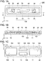
- Fig. 1A and 1C are abbreviated top and bottom views of a light emitting device for the first mode of implementation, and Fig. 1B is an abbreviated cross-section view through line A-A in Fig. 1A .
- the light emitting device 200 for the first mode of implementation is primarily configured with light emitting elements 30 mounted in a light emitting device package 100 and enclosed by encapsulating material 50.
- the encapsulating material 50 of the present example includes fluorescent material 60, the fluorescent material 60 can be omitted.
- the package 100 as viewed from above has a shape with a long dimension in one direction.
- the package 100 when viewed from above, has a longitudinal direction and a (shorter) transverse, transverse direction perpendicular to the longitudinal direction.
- the longitudinal direction is the direction parallel to the lead-frame package sides that extend in the long direction (which are the outer surfaces of the package normal to the transverse direction) as viewed from above.
- the longitudinal direction of the package is the x-direction
- the transverse direction is the y-direction
- the up and down (vertical) direction is the z-direction.
- the x-direction is the length direction
- the y-direction is the width direction
- the z-direction is the thickness direction.
- the package 100 shown in Figs. 1A-C is provided with two lead-frames 11, 12, and molded resin 20 holds the two lead-frames integrally.
- a third lead-frame 13 is provided between the two lead-frames 11, 12, and molded resin 20 holds the three lead-frames 11, 12, 13 integrally.
- the two lead-frames 11, 12 are lined-up in the longitudinal direction of the package 100.
- Each of the lead-frames 11, 12, 13 is shaped with a long dimension in the longitudinal direction (x-direction) similar to the shape of the package 100.
- the lead-frames 11, 12, 13 have a plate (sheet-metal) form with practically no processing such as bending or folding implemented.
- the two lead-frames 11, 12 (more specifically, the three lead-frames 11, 12, 13) have a gap region that separates the lead-frames.
- the gap region is filled with the molded resin 20, and the molded resin 20 holds the lead frames integrally with the gap region as an electrical isolation region.
- At least parts of the bottom surfaces of the three lead-frames 11, 12, 13 are exposed from the molded resin 20 and together with the molded resin 20 form the bottom surface of the package 100.
- This achieves a package with superior surface mounting characteristics with conducting mounting adhesive and superior thermal dissipation characteristics.
- the light emitting elements are mounted on the upper surface of the package 100.
- the lead-frame on the right side is called the first lead-frame 11
- the lead-frame on the left side is called the second lead-frame 12
- the lead-frame between those two lead-frames 11, 12 is called the third lead-frame 13.
- the molded resin 20 has a rectangular shape (as viewed from above) that extends in the longitudinal direction (x-direction) of the package.
- the molded resin 20 covers the edges (except for pre-molding support structure 104 edges) of the lead-frames (i.e. the three lead-frames 11, 12, 13).
- the molded resin 20 covers part (in particular, periphery regions) of the upper surfaces of the lead-frames (i.e. the three lead-frames 11, 12, 13). Further, the molded resin 20 together with the lead-frames (i.e. the three lead-frames 11, 12, 13) forms a cavity to hold the light emitting elements.
- the bottom of the cavity is formed by the upper surfaces of the lead-frames 11, 12, 13 and the surface of the molded resin 20.
- Side-wall surfaces of the cavity are formed by surfaces of the molded resin 20.
- the cavity side-wall surfaces can be vertical, tapered side-wall surfaces that reduce the size of the cavity opening towards the bottom of the cavity are preferable for efficiently extracting light emitted by the light emitting elements.
- an example of a package with a cavity is presented, but it is also possible, for example, to make a flat package with no cavity and no side-walls 23 (and that type of package can be applied in other modes of implementation).
- the first lead-frame 11 has a main body 101 and an extension 102 that extends towards the second lead-frame 12 from the main body 101 with a narrowed width.
- a recess 103 is established in the bottom surface of the extension 102 of the first lead-frame 11.
- the recess 103 is filled with molded resin 20.
- the recess 103 filled with the molded resin 20 separates at least part of the exposed region 107 of the bottom surface of the extension 102 from the exposed region 105 of the bottom surface of the main body 101.
- the main body 101 can be considered as the primary part of the lead-frame and includes the region of the upper surface where a light emitting element is mounted.
- the extension 102 can also vary in width as it extends from the main body 101.
- the boundary between the main body 101 and the extension 102 can be considered to be, for example, a straight-line in the transverse y-direction passing through the point where width of the lead-frame 11 changes.
- the depth of the recess 103 is determined in view of molded resin infilling and lead-frame strength and is, for example, preferably greater than or equal to 1mm and less than or equal to approximately half the maximum thickness of the lead-frame.
- the exposed region 105 of the bottom surface of the main body of the lead-frame 11 is separated from at least part of the exposed region 107 of the bottom surface of the extension, and the separated exposed regions are formed in the shape of islands surrounded by the molded resin 20.
- This can improve symmetry of the exposed regions of the bottom surfaces of the lead-frames and can improve the surface area uniformity of those exposed regions. Accordingly, when the package 100 is surface mounted with conducting mounting adhesive, uneven conducting mounting adhesive application can be controlled and inclined package 100 mounting can be curtailed. Further, the self-aligning capability of the package 100 can be enhanced.
- bonding wires 40 from the light emitting elements 30 and protection device 70 or the protection device 70 itself can be attached to the upper surface of the extension 102. This allows the bonding wires 40 to be made relatively short, and can alleviate light reduction due to the bonding wires 40 to increase light extraction efficiency.
- the maximum width (the maximum dimension in the transverse y-direction, for example, the width of the main body of the lead-frame) of the two lead-frames 11, 12 can be different, it is preferable for the maximum widths to be approximately the same.
- the two lead-frames 11, 12 can be oriented at a skewed angle with respect to each other (as viewed from above), it is preferable for the lead-frames to be disposed approximately parallel to each other.
- lead-frames 11, 12 can be disposed with their longitudinal (x-direction) centerlines shifted in the transverse y-direction (as viewed from above), it is preferable for the lead-frames to be disposed with their longitudinal (x-direction) centerlines approximately aligned (in a single straight-line).
- the following describes a preferable implementation of the light emitting device package 100 and light emitting device 200.
- essentially the entire exposed region 107 of the bottom surface of the extension 102 is preferable for essentially the entire exposed region 107 of the bottom surface of the extension 102 to be separated from the exposed region 105 of the bottom surface of the main body 101 by molded resin 20 filling the recess 103.
- This configuration can be realized by establishing the recess 103 on the bottom surface of the extension 102 next to the main body 101 (as shown in the figures), on the bottom surface of the main body 101 next to the extension 102, or along the boundary between the main body 101 and the extension 102.
- the exposed region 105 of the bottom surface of the main body 101 and the exposed region 107 of the bottom surface of the extension 102 can be clearly separated. This produces an advantageous layout of the exposed regions 105, 107 of the main body 101 and extension 102 to further improve the symmetry and surface area uniformity of exposed regions of the bottom surfaces of the lead-frames, and further enhance the self-aligning capability of the package.
- the first lead-frame 11 of the package 100 has an extension 102.
- the package 100 has the third lead-frame 13 established opposite (in the transverse y-direction) the extension 102 of the first lead-frame 11. At least part of the bottom surface of the third lead-frame 13 is exposed from the molded resin 20. Since this configuration establishes an exposed region 109 of the bottom surface of the third lead-frame opposite the exposed region 107 of the bottom surface of the extension of the first lead-frame, it can improve the symmetry and surface area uniformity of exposed regions of the bottom surfaces of the lead-frames.
- the exposed region 107 of the bottom surface of the extension of the first lead-frame is established in an approximately rectangular shape. This makes it easy to improve the symmetry and surface area uniformity of exposed regions of the bottom surfaces of the lead-frames, and makes it easy to enhance the self-aligning capability of the package.
- the exposed region 109 of the bottom surface of the third lead-frame 13 is also established in an approximately rectangular shape. This enables the exposed region 109 to balance with the exposed region 107 of the bottom surface of the extension of the first lead-frame to improve the symmetry and surface area uniformity of exposed regions of the bottom surfaces of the lead-frames and improve package self-alignment.
- the exposed region 109 of the bottom surface of the third lead-frame 13 is formed in approximately the same (rectangular) shape as the exposed region 107 of the bottom surface of the extension of the first lead-frame (as shown in the figures). Further, the exposed region 105 of the bottom surface of the main body of the first lead-frame and the exposed region 106 of the bottom surface of the second lead-frame 12 (which can be viewed as the main body of the second lead-frame) are also established in approximately rectangular shapes. This can further improve the symmetry and surface area uniformity of exposed regions of the bottom surfaces of the lead-frames and further improve package self-alignment.
- transverse (y-direction) linear symmetry is obtained about the longitudinal (x-direction) centerline of the package. It is also clear that longitudinal (x-direction) symmetry is obtained about a line in the y-direction through the center of the package. This can still further improve the symmetry and surface area uniformity of exposed regions of the bottom surfaces of the lead-frames and further improve package self-alignment.
- the exposed regions of the bottom surfaces of the lead-frames can have rounded or truncated corners due to lead-frame processing such as beveling.
- the extension 102 of the first lead-frame is positioned approximately in the center of the package 100 in the longitudinal (x-direction). Positioning the extension 102 approximately at the longitudinal center of the package 100 makes it easy to mount light emitting elements on each of the two lead-frames 11, 12 and makes it easy to control luminance distribution characteristics. Further, the third lead-frame 13 is disposed opposite the extension 102 in the transverse y-direction of the package 100. Consequently, even when light emitting elements 30 are mounted on the first and second lead-frames 11, 12 respectively, bonding wires 40 connected to the third lead-frame 13 can be made relatively short. This configuration makes it easy to alleviate light reduction due to the bonding wires 40 and increase light extraction efficiency.
- the protection device 70 can be mounted on the upper surface of the first lead-frame extension 102. This makes it easy to increase the separation between the light emitting elements 30 and the protection device 70. Thus, light reduction due to the protection device 70 is easy to alleviated, so that the light extraction efficiency can be increased easily. Further, since the bonding wire 40 connecting the protection device 70 to the second lead-frame 12 can be made relatively short, light reduction due to the bonding wire 40 can be alleviated and light extraction efficiency can be easily improved.
- the light emitting device 200 is provided with a light emitting device package 100 and light emitting elements 30 mounted on the upper surfaces of the first and second lead-frames 11, 12 respectively.
- the separation between the two light emitting elements 30 can be made relatively large and favorable luminance distribution characteristics can be obtained.
- the upper surface of the third lead-frame 13 is connected by a bonding wire 40 to the light emitting element 30 mounted on the first lead-frame 11, and is connected by another bonding wire 40 to the light emitting element 30 mounted on the second lead-frame 12.
- the light emitting device 200 is provided with a protection device 70 mounted on the upper surface of the first lead-frame extension 102.
- the protection device 70 is connected to the upper surface of the second lead-frame 12 by a bonding wire 40.
- Mounting the protection device 70 on the upper surface of the first lead-frame extension 102 makes it easy to increase separation between the protection device 70 and the light emitting elements 30.. Thus, it becomes easy to alleviate light reduction due to the protection device 70, and thus to increase light extraction efficiency.
- the bonding wire 40 connecting the protection device 70 to the second lead-frame 12 can be made relatively short, light reduction due to the bonding wire 40 can be alleviated and light extraction efficiency can be easily improved.
- Fig. 2A and 2C are abbreviated top and bottom views of a light emitting device for the second mode of implementation
- Fig. 2B is an abbreviated cross-section view through line B-B in Fig. 2A
- the light emitting device 220 for the second mode of implementation is primarily configured with light emitting elements 30 mounted in a light emitting device package 120 and enclosed by encapsulating material 50.
- the encapsulating material 50 of the present example includes fluorescent material 60, the fluorescent material 60 can be omitted.
- the package 120 shown in Figs. 2A-C is provided with five lead-frames 11, 12, 13, 14, 15 and molded resin 20 holds the five lead-frames integrally.
- the five lead-frames 11, 12, 13, 14, 15 are lined-up in the longitudinal direction (x-direction) of the package 120.
- Each of the lead-frames 11, 12, 13, 14, 15 is shaped with a long dimension in the longitudinal direction (x-direction) similar to the shape of the package 120.
- the lead-frames 11, 12, 13, 14, 15 have a plate (sheet-metal) form with practically no processing such as bending or folding implemented.
- the five lead-frames 11, 12, 13, 14, 15 have gap regions that separate the lead-frames and are filled with the molded resin 20.
- the molded resin 20 holds lead flames integrally with the gap regions as electrical isolation regions. At least parts of the bottom surfaces of the five lead-frames 11, 12, 13, 14, 15 are exposed from the molded resin 20 and together with the molded resin 20 form the bottom surface of the package 120. This achieves a package with superior surface mounting characteristics with conducting mounting adhesive and superior thermal dissipation characteristics. Note that the light emitting elements are mounted on the upper surface of the package 120.
- the lead-frame in the center is called the first lead-frame 11
- the lead-frame furthest to the left is called the second lead-frame 12
- the lead-frame between the first lead-frame 11 and the second lead-frame 12 is called the third lead-frame 13
- the lead-frame furthest to the right is called the fourth lead-frame 14
- the lead-frame between the first lead-frame 11 and the fourth lead-frame 14 is called the fifth lead-frame 15.
- the molded resin 20 has a rectangular shape (as viewed from above) that extends in the longitudinal direction (x-direction) of the package.
- the molded resin 20 covers the edges (except for pre-molding support structure 104 edges) of the lead-frames 11, 12, 13, 14, 15.
- the molded resin 20 covers part (in particular, periphery regions) of the upper surfaces of the lead-frames 11, 12, 13, 14, 15.
- the molded resin 20 together with the lead-frames 11, 12, 13, 14, 15 forms a cavity to hold the light emitting elements. Specifically, the bottom of the cavity is formed by the upper surfaces of the lead-frames 11, 12, 13, 14, 15 and the surface of the molded resin 20.
- Side-wall surfaces of the cavity are formed by surfaces of the molded resin 20.
- the cavity side-wall surfaces can be vertical, tapered side-wall surfaces that reduce the size of the cavity opening towards the bottom of the cavity are preferable for efficiently extracting light emitted by the light emitting elements.
- the first lead-frame 11 has a main body 101, a first extension 102 that extends towards the second lead-frame 12 from the main body 101 with a narrowed width, and a second extension 102 that extends towards the fourth lead-frame 14 from the main body 101 with a narrowed width.
- recesses 103 are established in the bottom surfaces of the first and second extensions 102 of the first lead-frame 11.
- the recesses 103 are filled with molded resin 20.
- the recesses 103 filled with molded resin 20 separate at least parts of the exposed regions 107 of the bottom surfaces of the first and second extensions 102 from the exposed region 105 of the bottom surface of the main body 101.
- the exposed region 105 of the bottom surface of the main body of the first lead-frame 11 is separated from at least parts of the exposed regions 107 of the bottom surfaces of the first and second extensions 102, and exposed region105 and the exposed region 107 are formed in the shape of islands (surrounded by the molded resin 20).
- This can improve symmetry of the exposed regions of the bottom surfaces of the lead-frames and thus can improve the surface area uniformity of those exposed regions. Accordingly, when the package 120 is surface mounted with conducting mounting adhesive, uneven conducting mounting adhesive application can be controlled and inclined package 120 mounting can be curtailed. Further, the self-aligning capability of the package 120 can be enhanced.
- first and second extensions 102 of the first lead-frame 11 extend towards the second and fourth lead-frames 12, 14 respectively, bonding wires 40 from the light emitting elements 30 and protection device 70 or the protection device 70 itself can be attached to the upper surfaces of the extensions 102. This allows the bonding wires 40 to be made relatively short, and can alleviate light reduction due to the bonding wires 40 to increase light extraction efficiency.
- the maximum width (the maximum dimension in the transverse y-direction, for example, the width of the main body of a lead-frame) of the first, second, and fourth lead-frames 11, 12, 14 can be different, it is preferable for the maximum widths to be approximately the same.
- the first, second, and fourth lead-frames 11, 12, 14 can be oriented at skewed angles with respect to each other (as viewed from above), it is preferable for the lead-frames to be disposed approximately parallel to each other.
- first, second, and fourth lead-frames 11, 12, 14 can be disposed with their longitudinal (x-direction) centerlines shifted in the transverse y-direction (as viewed from above), it is preferable for the lead-frames to be disposed with their longitudinal (x-direction) centerlines approximately aligned (in a single straight-line).
- the following describes a preferable implementation of the light emitting device package 120 and light emitting device 220.
- the package 120 has the third and fifth lead-frames disposed opposite (in the transverse y-direction) the first and second extensions 102 respectively of the first lead-frame 11. Since this configuration establishes exposed regions 109 of the bottom surfaces of the third and fifth lead-frames opposite exposed regions 107 of the bottom surfaces of the first and second extensions (respectively) of the first lead-frame, it can improve the symmetry and surface area uniformity of exposed regions of the bottom surfaces of the lead-frames.
- the exposed regions 107 of the bottom surfaces of the first and second extensions of the first lead-frame are established in approximately rectangular shapes.
- the exposed regions 109 of the bottom surfaces of the third and fifth lead-frames 13, 15 are also established in approximately rectangular shapes.
- the exposed region 105 of the bottom surface of the main body of the first lead-frame and the exposed regions 106 of the bottom surfaces of the second and fourth lead-frames 12, 14 which can be viewed as main bodies are also established in approximately rectangular shapes.
- the upper surface of the third lead-frame 13 is connected by a bonding wire 40 to the light emitting element 30 mounted on the first lead-frame 11, and is connected by another bonding wire 40 to the light emitting element 30 mounted on the second lead-frame 12.
- the upper surface of the fifth lead-frame 15 is connected by a bonding wire 40 to the light emitting element 30 mounted on the first lead-frame 11, and is connected by another bonding wire 40 to the light emitting element 30 mounted on the fourth lead-frame 14. This connects the three light emitting elements 30 in series.
- the third and fifth lead-frames 13, 15 are advantageously utilized to connect light emitting elements 30 mounted on the first, second, and fourth lead-frames 11, 12, 14 in series, and this allows the length of the bonding wires 40 to be made relatively short.
- the light emitting device 220 has a protection device 70 mounted on the upper surface of the first extension 102 of the first lead-frame and the protection device 70 is connected to the second lead-frame 12 by a bonding wire 40.
- This allows the bonding wire 40 connecting the protection device 70 and the lead-frame to be made relatively short, and can alleviate light reduction due to the bonding wire 40 making it easy to increase the light extraction efficiency.
- the upper surface of the second extension 102 of the first lead-frame and the upper surface of the fourth lead-frame 14 are connected by a bonding wire 40. This allows the protection device 70 to be connected in parallel with respect to the light emitting elements 30. Note that since the package 120 has the second extension 102 of the first lead-frame connected to the fourth lead-frame 14, the first lead-frame 11 and the fourth lead-frame 14 can also be made as a single-piece.
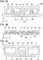
- Fig. 3A and 3C are abbreviated top and bottom views of a light emitting device for the third mode of implementation, and Fig. 3B is an abbreviated cross-section view through line C-C in Fig. 3A .
- the light emitting device 230 for the third mode of implementation is primarily configured with light emitting elements 30 mounted in a light emitting device package 130 and enclosed by encapsulating material 50.
- the encapsulating material 50 of the present example includes fluorescent material 60, the fluorescent material 60 can be omitted.
- the package 130 shown in Figs. 3A-C is provided with two lead-frames 11, 12, and molded resin 20 holds the two lead-frames integrally.
- the two lead-frames 11, 12 are lined-up in the longitudinal x-direction of the package 130.
- Each of the lead-frames 11, 12 is shaped with a long dimension in the longitudinal direction (x-direction) similar to the shape of the package 130.
- the lead-frames 11, 12 have a plate (sheet-metal) form with practically no processing such as bending or folding.
- the two lead-frames 11, 12 have a gap region that separates the lead-frames. The gap region is filled with the molded resin 20, and the molded resin 20 holds the lead frames integrally by molded resin 20 with the gap region as an electrical isolation region.
- At least parts of the bottom surfaces of the two lead-frames 11, 12 are exposed from the molded resin 20 and together with the molded resin 20 form the bottom surface of the package 130.
- the light emitting elements are mounted on the upper surface of the package 130.
- the lead-frame on the right side is called the first lead-frame 11
- the lead-frame on the left side is called the second lead-frame 12.
- the molded resin 20 has a rectangular shape (as viewed from above) that extends in the longitudinal direction (x-direction) of the package.
- the molded resin 20 covers the edges (except for pre-molding support structure 104 edges) of the two lead-frames 11, 12.
- the molded resin 20 covers part (in particular, periphery regions) of the upper surfaces of the two lead-frames 11, 12.
- the molded resin 20 together with the two lead-frames 11, 12 forms cavities to hold the light emitting elements.
- the bottoms of the cavities are formed by the upper surfaces of the lead-frames 11, 12 and surfaces of the molded resin 20.
- Side-wall surfaces of the cavities are formed by surfaces of the molded resin 20.
- cavity side-wall surfaces can be vertical, tapered side-wall surfaces that reduce the size of each cavity opening towards the bottom of the cavity are preferable for efficiently extracting light emitted by the light emitting elements.
- the first lead-frame 11 has a main body 101 and an extension 102 that extends towards the second lead-frame 12 from the main body 101 with a narrowed width.
- a recess 103 is established in the bottom surface of the extension 102, and the recess 103 is filled with molded resin 20.
- the recess 103 filled with molded resin 20 separates at least part of the exposed region 107 of the bottom surface of the extension 102 from the exposed region 105 of the bottom surface of the main body 101.
- the exposed region 105 of the bottom surface of the main body 101 of the first lead-frame 11 is separated from at least part of the exposed region 107 of the bottom surface of the extension 102, and the exposed region 105 and the exposed region 107 are formed in the shape of islands (surrounded by the molded resin 20).
- This can improve symmetry of the exposed regions of the bottom surfaces of the lead-frames and can improve the surface area uniformity of those exposed regions. Accordingly, when the package 130 is surface mounted with conducting mounting adhesive, uneven conducting mounting adhesive application can be controlled and inclined package 130 mounting can be curtailed. Further, the self-aligning capability of the package 130 can be enhanced.
- bonding wires 40 from the light emitting elements 30 and protection device 70 or the protection device 70 itself can be attached to the upper surface of the extension 102. This allows the bonding wires 40 to be made relatively short, and thus can alleviate light reduction due to the bonding wires 40 to increase light extraction efficiency.
- the maximum width (the maximum dimension in the transverse y-direction, for example, the width of the main body of the lead-frame) of the two lead-frames 11, 12 can be different, it is preferable for the maximum widths to be approximately the same.
- the two lead-frames 11, 12 can be oriented at a skewed angle with respect to each other (as viewed from above), it is preferable for the lead-frames to be disposed approximately parallel to each other.
- the two lead-frames 11, 12 can be disposed with their longitudinal (x-direction) centerlines shifted in the transverse y-direction (as viewed from above), it is preferable for the lead-frames to be disposed with their lengthwise (x-direction) centerlines approximately aligned (in a single straight-line).
- the following describes a preferable implementation of the light emitting device package 130 and light emitting device 230.
- the second lead-frame 12 has a main body 101 and an extension 102 that extends towards the first lead-frame 11 from the main body 101 with a narrowed width.
- a recess 103 is established in the bottom surface of the second lead-frame 12, and the recess 103 is filled with molded resin 20.
- the recess 103 in the second lead-frame 12 filled with the molded resin 20 separates at least part of the exposed region 107 of the bottom surface of the extension 102 of the second lead-frame 12 from the exposed region 105 of the bottom surface of the main body 101 of the second lead-frame 12.
- the extensions 102 of the first and second lead-frames 11, 12 are disposed opposite each other in transverse y-direction.
- the exposed region 107 of the extension 102 of the first lead-frame 11 and the exposed region 107 of the extension 102 of the second lead-frame 12 are established opposite each other, the symmetry and surface area uniformity of exposed regions of the bottom surfaces of the lead-frames can be improved. Further improvement results when the exposed region 107 of the extension 102 of the first lead-frame 11 and the exposed region 107 of the extension 102 of the second lead-frame 12 are made in approximately the same shape.
- the exposed regions 107 of the bottom surfaces of the first and second lead-frames 11, 12 are established in approximately rectangular shapes. Further, the exposed regions 105 of the bottom surfaces of the main bodies of the first and second lead-frames 11, 12 are also established in approximately rectangular shapes.
- the overall pattern of lead-frame exposed regions on the bottom surface of the package 130 is examined, it is clear that symmetry is obtained both transversally (in the y-direction) about the lengthwise (x-direction) centerline of the package and longitudinally (in the x-direction) about a line in the y-direction through the center of the package.
- this type of structure makes it easy to improve the symmetry and surface area uniformity of exposed regions of the bottom surfaces of the lead-frames, and makes it easy to enhance the self-aligning capability of the package 130.
- the exposed regions of the bottom surfaces of the lead-frames can have rounded or truncated corners due to lead-frame processing such as beveling.
- the extension 102 of the first lead-frame 11 is connected by a bonding wire 40 to the light emitting element 30 mounted on the second lead-frame 12, and the extension 102 of the second lead-frame 12 is connected by a bonding wire 40 to the light emitting element 30 mounted on the first lead-frame 11.
- a protection device 70 is mounted on the upper surface of the first lead-frame extension 102.
- the protection device 70 is connected to the upper surface of the extension 102 of the second lead-frame 12 by a bonding wire 40.
- the molded resin 20 on the top of the package 130 has partition walls 25 extending in the transverse y-direction that partition and expose at least part of the upper surface of the main body 101 of the first lead-frame 11 and at least part of the upper surface of the extension 102 of the first lead-frame 11 at the second lead-frame 12 end. Accordingly, while maintaining the utility of the upper surfaces of the extensions 102, the main body 101 of the first lead-frame 11 can be partitioned from the main body 101 of the second lead-frame 12 by the partition walls 25.
- partition walls 25 This allows the partition walls 25 to reflect light emitted by the light emitting elements 30 in an upward direction, and alleviate light reduction due to the light emitting elements 30, protection device 70 and their associated bonding wires 40 to those elements, which are disposed. Thus, the light extraction efficiency can be improved.
- the partition walls 25 are formed in a continuous manner with the molded resin 20 cavity side-walls 23. Accordingly, the partition walls 25 act in a manner pressing downward on the upper surfaces of the lead-frames and can serve to suppress lead-frame delamination from the molded resin 20. Note that partition walls 25 can be established at least on the first lead-frame 11 side, or at least on the second lead-frame 12 side.
- partition walls 25 it is preferable to establish partition walls 25 over the extension 102 of the first lead-frame 11. Since the extensions 102 are established near the gap region between the two lead-frames at the center of the package, it is easy to separate device mounting regions inside package cavities, for example equally, via partition walls 25, and this allows desirable luminance distribution characteristics to be obtained. Further, the partition walls 25 can effectively suppress lead-frame delamination from the molded resin 20 by acting in a manner that holds down the lead-frame extensions 102.
- the partition walls 25 include a first partition wall and a second partition wall that straddle the tops of the extensions 102 of the first and second lead-frames 11, 12.
- the upper surfaces of the extensions 102 of the first and second lead-frames 11, 12 are partitioned into three regions by the first and second partition walls. Cavity interiors are divided in the longitudinal x-direction into three regions, which are a left-side region, a center region, and a right-side region. Accordingly, the upper surfaces of the ends of the extensions 102 of the first and second lead-frames 11, 12 are exposed in the left-side region and the right-side region respectively.
- Wires 40 connected to the light emitting elements 30 are connected to the end of each extension 102.
- a protection device 70 is disposed in the cavity center region.
- the first and second partition walls 25 in a manner surrounding the protection device 70, light reduction due to the protection device 70 and its associated bonding wire 40 can be alleviated and light extraction efficiency can be improved.
- a bonding wire 40 straddles a partition wall 25
- partition wall 25 straddling it is preferable to make partition walls approximately the same height as the upper surface of the molded resin 20 (i.e. the upper surfaces of the cavity side-walls 23).
- partition walls 25 can also be used in the light emitting device packages for other modes of implementation.
- a partition wall 25 can be established approximately in the center of the package 100 for the first mode of implementation.
- partition walls 25 can be established approximately in the center of the third lead-frame 13 (approximately in the center of the first extension 102 of the first lead-frame) and approximately in the center of the fifth lead-frame 15 (approximately in the center of the second extension 102 of the first lead-frame).
- the protection device 70 and associated bonding wire 40 can be filled with a partition wall 25.
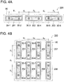
- Figs. 4A and 4B are abbreviated plan views showing examples of the layout of light emitting devices for illumination devices of the fourth mode of implementation.
- the illumination devices shown in Figs. 4A and 4B are provided with a plurality of light emitting devices and substrate material on which the light emitting devices are mounted.
- the light emitting devices are surface mounted on the substrate material using conducting mounting adhesive.
- the illumination device 300 example shown in Fig. 4A has a plurality of light emitting devices 201-203 arranged in a one-dimensional array (arranged in a line) on substrate material 80. More specifically, the illumination device 300 has three light emitting devices 201, 202, 203 lined up lengthwise at approximately equal intervals.
- the illumination device 320 example shown in Fig. 4B has a plurality of light emitting devices 201-208 arranged in a two-dimensional array (arranged in rows and columns) on substrate material 80. More specifically, the illumination device 320 has eight light emitting devices 201-208 arranged at approximately equal intervals in two rows and four columns with the package longitudinal direction aligned in the column direction and the transverse direction aligned in the row direction.
- any type of light emitting device e.g.
- any commonly known light emitting device can be used for the light emitting devices 201-208 in these illumination devices 300, 320, it is preferable to use the light emitting devices of the present invention (e.g. light emitting devices 200, 220, 230 of the first, second, and third modes of implementation).
- the number of light emitting devices mounted in a single illumination device and the number of light emitting elements mounted in a single light emitting device are set here only as one example.
- the distance d 1 in the longitudinal direction of the package between the first light emitting element 30-2 in the first light emitting device 201 (disposed closest to the second light emitting device 202) and the second light emitting element 30-3 in the second light emitting device 202 (disposed closest to the first light emitting device 201) is approximately equal to the distance p 1 between the first light emitting element 30-2 in the first light emitting device 201 and the adjacently disposed third light emitting element 30-1. This is designed to achieve an approximately uniform luminance distribution across adjacently disposed light emitting devices. In the example of Fig.
- the distance s 1 in the transverse direction of the package between the first light emitting element 30-2 (or the third light emitting element 30-1) in the first light emitting device 201 and the sixth light emitting element 30-6 (or the fifth light emitting element 30-5) in the third light emitting device 203 is approximately equal to the distance d 1 .
- the distances s 2 and s 3 for adjacently arrayed light emitting devices are also made equal to the distance d 1 .
- the distance p 1 in the longitudinal direction of the package between the light emitting elements 30-1, 30-2 in the first light emitting device 201 is approximately equal to the distance p 2 between the light emitting elements 30-3 and 30-4 in the second light emitting device 202.
- the light emitting elements mounted in different light emitting devices can be considered to be disposed at equal intervals over the surface of the substrate material, it is desirable to make the interval between light emitting elements in each light emitting device relatively large.
- the distance between the light emitting elements in the same light emitting device is made large, there is a tendency to form long bonding wires to connect the light emitting elements and protection device. Since the light emitting device of the present invention allows the bonding wires connecting the light emitting elements and protection device to be made relatively short, it can be used to advantage in this type of illumination device.
- the present invention can control uneven conducting mounting adhesive application and achieve a high degree of package self-alignment, undesirable package rotation and inclined mounting are suppressed, and thus light emitting devices can be mounted in proper orientation on the substrate material. This achieves superior accuracy for positioning light emitting devices (and, consequently, light emitting elements), and makes it easy to achieve precise light distribution characteristics.
- Metal materials that can conduct electricity and can be connected with the light emitting elements and protection device can be used as the lead-frames.
- metals such as copper, aluminum, gold, silver, tungsten, iron (steel), nickel, cobalt, molybdenum, alloys of those metals, copper-iron alloy, and phosphor bronze can be used in sheet metal form processed by various methods such as press-forming, etching, and metal rolling.
- metal plating or light reflecting thin-film can be established on the surface of those metals with materials such as silver, aluminum, rhodium, gold, copper, and their alloys.
- silver which has the best light reflecting characteristics, is preferable.
- lead-frame thickness can be freely selected, for example, it is greater than or equal to 0.1mm and less than or equal to 1 mm, and preferably greater than or equal to 0.2mm and less than or equal to 0.4mm.
- grooves and recesses can be formed in perimeter regions of the upper and lower surfaces of the lead-frames that make contact with the molded resin. This can restrain the ingress of ambient moisture and/or flux included in the conducting mounting adhesive, and can improve intimate contact between the molded resin and the lead-frames.
- the base material (matrix) of the molded resin can be a thermosetting resin such as polybismaleimide-triazine resin, epoxy resin, silicone resin, denatured silicone resin, silicone-based resin, polyimide resin, or polyurethane resin.
- the base material can be a thermoplastic resin such as aliphatic polyamide resin, semi-aromatic polyamide resin, polyethylene terephthalate, polycyclohexane terephthalate, liquid crystal polymer, polycarbonate resin, syndiotactic polystyrene, polyphenylene-ether, polyphenylene-sulfide, polyether-sulfone resin, polyether-ketone, or polyarylate resin.
- particulate or fiber fillers and pigments such as glass, silica, titanium oxide, magnesium oxide, magnesium carbonate, magnesium hydroxide, calcium carbonate, calcium hydroxide, calcium silicate, magnesium silicate, wollastonite, mica, zinc oxide, barium titanate, calcium titanate, aluminum borate, aluminum oxide, silicon carbide, antimony oxide, zinc stannate, zinc borate, iron oxide, chrome oxide, manganese oxide, and carbon black can be mixed into the base material.
- Light emitting semiconductor devices such as light emitting diodes (LEDs) and semiconductor laser diodes can be used as the light emitting elements.
- a light emitting element can be any of a variety of semiconductor structures configured with a pair of positive and negative electrodes.
- nitride semiconductor light emitting elements e.g. In x Al y Ga 1-x-y N, 0 ⁇ x, 0 ⁇ y, x+y ⁇ 1 that can efficiently excite fluorescent material are preferable.
- the light emitting elements can be gallium arsenide based or gallium phosphide based semiconductors that emit light from green to red wavelengths.
- the chip is mounted with the electrode surface up and with bonding wires connecting each electrode to a lead-frame.
- the bottom side electrode is connected to a lead-frame via conducting adhesive (die-attach) and the upper surface electrode is connected to a lead-frame via a bonding wire.
- a metal layer such as silver or aluminum, or a light-reflecting dielectric layer on the die-attachment surface side of the light emitting element.
- a single light emitting element or a plurality of light emitting elements can be mounted in a single light emitting device package, and the size, shape, and light emission wavelength of the light emitting elements can be selected freely.
- a plurality of light emitting elements can be connected in series or parallel via the lead-frames and/or bonding wires.
- a combination of different wavelength light emitting elements such as one blue light emitting element and one red light emitting element (two element), one blue light emitting element and one green light emitting element (two element), or one blue light emitting element, one green light emitting element, and one red light emitting element (three element) combination can also be mounted in a single light emitting device package.
- the bonding wires are conducting wires that connect light emitting element and protection device electrodes with the lead-frames.
- metal wire including gold, copper, silver, platinum, aluminum, and alloys of those metals can be used.
- gold wire which can withstand stress applied by the encapsulating material without breaking and is superior with respect to characteristics such as thermal resistance, is preferable.
- the bonding wires can be configured with silver at least on the surface.
- the encapsulating material is material that encapsulates the light emitting elements, protection device, bonding wires etc. and protects them from dust (particulates), moisture, and external forces.
- the base material of the encapsulating material can be material that is electrically insulating and can transmit light emitted by the light emitting elements (preferably with a light transmissivity greater than or equal to 70%).
- silicone resin epoxy resin, phenol resin, polycarbonate resin, acrylic resin, polymethyl-pentene resin (Mitsui Chemical brand name: TPX resin), polynorbornene resin, modified (denatured) resin derived from those resins, or hybrid resin including one or more of those resins can be used. Glass can also be used.
- the encapsulating material can also have particles with various functions such as filler and fluorescent material added into the base material.
- Filler can be material such as light dispersing agents or coloring pigments.
- filler can be silica, titanium oxide, magnesium oxide, magnesium carbonate, magnesium hydroxide, calcium carbonate, calcium hydroxide, calcium silicate, zinc oxide, barium titanate, aluminum oxide, iron oxide, chrome oxide, manganese oxide, glass, and carbon black.
- Filler particles can be round or crushed with arbitrary shape, and the encapsulating material can include hollow regions or can be porous.
- the fluorescent material absorbs at least part of the (primary beam of) light emitted from the light emitting element and re-emits (secondary) light at a wavelength different from that of the primary beam.
- the fluorescent material can be nitride and oxy-nitride system fluorescent materials primarily activated by lanthanoid-group rare earth elements such as europium and cerium.
- the fluorescent material can be substances such as europium-activated ⁇ or ⁇ -sialon fluorescent material, various alkaline earth metal nitride silicate fluorescent materials, lanthanoid-group elements such as europium, alkaline earth metal halogen-apatite fluorescent materials primarily activated by transition metal group elements such as manganese, alkaline earth halo-silicate fluorescent materials, alkaline earth metal silicate fluorescent materials, alkaline earth metal halogen borate fluorescent materials, alkaline earth metal aluminate fluorescent materials, alkaline earth metal silicates, alkaline earth metal sulfides, alkaline earth metal thiogallates, alkaline earth metal silicon nitride, germinate, rare earth element aluminates primarily activated by lanthanoid-group elements such as cerium, and organic and organic complex materials primarily activated by rare earth element silicates or lanthanoid-group elements such as europium.
- transition metal group elements such as manganese
- Fluorescent materials other than those listed above but having similar functionality and effect can also be used. This allows realization of a light emitting device that outputs a combination of visible wavelength primary light mixed with secondary emitted colors (e.g. for white light output), or a light emitting device with fluorescent material excited by ultraviolet primary light that outputs secondary light at visible wavelengths.
- the fluorescent material can be settled towards the bottom of the package cavity or dispersed throughout the cavity.
- the protection device is a device to protect the light emitting elements from static (electricity) discharge and high-voltage surge.
- the protection device can be a Zener diode.
- it can be covered with reflective material such as a white resin.
- the substrate material is the material on which the light emitting devices (light emitting device packages) are mounted.
- the substrate material can be any of various circuit boards.
- the primary constituents of the circuit board substrate can be ceramics such as aluminum oxide (alumina) and aluminum nitride, metals such as copper and aluminum, and resins (including fiber reinforced resins) such as glass-epoxy, BT (bismaleimide-triazine) resin, and polyimide resin.
- Metal run or wire material can be copper, iron (steel), nickel, tungsten, chrome, aluminum, silver, gold, titanium and alloys of those metals.
- the metal run circuitry has lands (surface mounting regions) to mount the light emitting devices using conducting mounting adhesive.
- the pattern of metal run lands takes on approximately the same shape as the exposed regions of the bottom surfaces of the light emitting device lead-frames. This can suppress uneven conducting mounting adhesive application and improve light emitting device self-alignment.
- the conducting mounting adhesive is material for surface mounting light emitting devices on the substrate material.
- conducting mounting adhesive can be solder such as tin-bismuth, tin-copper, tin-silver, and gold-tin systems, or it can be metal paste (adhesive) that includes metals such as silver, gold, and palladium.
- the light emitting device for the first embodiment is a (top-view) surface mount device (SMD) light emitting diode (LED) having the structure of the light emitting device 200 example shown in Figs 1A-1C .
- SMD surface mount device
- LED light emitting diode
- the package 100 has a (solid) rectangular shape 7.0mm in length, 2.0mm in width, and 0.6mm in thickness.
- the package 100 has first and second lead-frames 11, 12 that make up the positive and negative electrodes and a third lead-frame between those lead-frames all formed as a single-piece with molded resin 20.
- Packages 100 are fabricated by loading a pre-processed sheet-metal plate, which has a plurality of lead-frame 11, 12, 13 groups connected by support structure leads (that form support structures 104 stubs after singulation) in a two-dimensional array, inside a mold cavity. Material that forms the molded resin 20 is introduced into the mold cavity in liquid form and hardened. After removal from the mold, each package is separated from the rest (singulated).
- the first lead-frame 11 is made up of a rectangular (as viewed from above) main body 101 with a 2.0mm length and 1.5mm width (neglecting support structure 104 stubs), and a rectangular (as viewed from above) extension 102 extending from the main body 101 towards the second lead-frame 12 with a 2.0mm length and 0.6mm width (neglecting support structure 104 stubs).
- the extension 102 is established on one side (in the transverse direction) of the main body 101 to give the first lead-frame 11 an L-shape (as viewed from above).
- the second lead-frame 12 is formed in a rectangular shape (as viewed from above) with a 2.0mm length and 1.5mm width (neglecting support structure 104 stubs).
- the third lead-frame 13 is disposed opposite the extension 102 of the first lead-frame 11 in the transverse direction, and is formed in a rectangular shape (as viewed from above) with a 1.8mm length and 0.6mm width (neglecting support structure 104 stubs).
- the width of the gap region (in the longitudinal direction) between the extension 102 of the first lead-frame 11 and the second lead-frame 12 is 0.5mm.
- the width of the gap region (in the longitudinal direction) between the main body 101 of the first lead-frame 11 and the third lead-frame 13 is also 0.5mm.
- the width of the gap region (in the transverse direction) between the extension 102 of the first lead-frame 11 and the third lead-frame 13 is 0.4mm. These gap regions are punched-out by press-processing sheet-metal.
- a recess 103 is established in the bottom surface of the first lead-frame 11 extension 102 immediately adjacent to the main body 101 with a 0.5mm length, 0.6mm width, and 0.15mm depth.
- the recess 103 is filled with molded resin 20. This separates essentially the entire exposed region 107 of the bottom surface of the extension from the exposed region 105 of the bottom surface of the main body of the first lead-frame 11 with molded resin 20 filling the recess 103.
- recesses having a depth of 0.09mm are formed around part of the perimeters of the bottom surfaces of the first and second lead-frames 11, 12 and around the entire perimeter of the bottom surface of the third lead-frame 13. These recesses are formed by etching and are also filled with molded resin 20.
- the exposed regions of the bottom surfaces of the three lead-frames are in practice coplanar with the bottom surface of the molded resin 20 and form the bottom surface of the package 100. Further, the exposed regions of the bottom surfaces of the three lead-frames have rectangular shapes (with rounded corners). Part of the ends of both the first and second lead-frames 11, 12 (which are also support structure 104 stubs) are exposed from the ends of the package 100 in the longitudinal direction. Recesses are formed in a continuous manner on the bottom surfaces at these exposed regions and function as castellations.
- the molded resin 20 is epoxy resin that includes titanium oxide molded into a rectangular shape (as viewed from above) with a length of 7.0mm, a width of 2.0mm, and a maximum thickness of 0.45mm.
- a cavity having a rectangular shape (with rounded corners) is formed approximately in the center of the upper surface of the molded resin 20 with a length of 6.4mm, width of 1.4mm, and depth of 0.35mm.
- the surfaces of the side-walls are inclined 5° to 30°. Grooves with a width of 0.12mm and a depth of 0.09mm are formed in the upper surfaces of the three lead-frames 11, 12, 13 along parts of the boundaries between the bottom of the cavity and the surfaces of the side-walls, and those grooves are filled with the molded resin 20.
- a light emitting element 30 is mounted with silicone resin insulating mounting adhesive (die-attach) on the upper surface of each of the first and second lead-frames 11, 12 that form the bottom of the cavity in the package 100.
- Each light emitting element 30 is a nitride semiconductor light emitting diode (LED) chip with an n-type layer, an active layer, and a p-type layer formed in that order on a sapphire substrate.
- the LED chip can output blue light (with a center wavelength of 460nm) and has dimensions 650 ⁇ m by 650 ⁇ m by 150 ⁇ m.
- the distance between the centers of the two light emitting element 30 die is 4.0mm.
- One of the (p or n) electrodes is connected via a bonding wire 40 to the lead-frame that the chip is mounted on, and the other (p or n) electrode is connected via a bonding wire 40 to the upper surface of the third lead-frame 13. This connects the two light emitting elements 30 in series.
- the bonding wires 40 are 25 ⁇ m diameter gold bonding wire.
- a 150 ⁇ m by 150 ⁇ m by 85 ⁇ m Zener diode protection device 70 die with opposing electrode structure (electrodes on the top and bottom surfaces) is mounted with silver mounting adhesive (conducting die-attach) on the upper surface of the extension 102 of the first lead-frame 11.
- the upper surface electrode of the protection device 70 is connected to the upper surface of the second lead-frame 12 via a bonding wire 40.
- the package 100 cavity with the two light emitting elements 30 and protection device 70 mounted inside is filled with encapsulating material 50 that covers each of the dies.
- the encapsulating material 50 includes silicone as a base material, cerium activated yttrium-aluminum-garnet (YAG:Ce) fluorescent material 60 and silica as filler.
- the upper surface of the encapsulating material 50 is approximately in the same plane as the upper surface of the molded resin cavity side-walls 23 making an essentially planar upper surface.
- the encapsulating material 50 is dispensed into the package 100 cavity in a fluid state and solidified by heating.
- the fluorescent material 60 settles towards the bottom of the cavity.
- the package and light emitting device configured as described above for the first embodiment can have the same effect as the package 100 and light emitting device 200 for the first mode of implementation.
- the light emitting device package of the present invention can be used with good results as a surface mount device (SMD) light emitting diode (LED) package.
- SMD surface mount device
- LED light emitting diode
- a light emitting device using the package of the present invention can be used in applications such as liquid crystal display backlighting, various illumination and lighting equipment, large-scale displays, and various display apparatus such as signs for advertisement and destination information.
- the light emitting device can also be used in image acquisition equipment such as digital video cameras, facsimile (FAX) machines, copy machines, and scanners, as well as in projectors.
- FAX facsimile
Description
- The present invention relates to a light emitting device package (also referred to simply as the package), to a light emitting device, and to an illumination device.
- As an example, Fig. 25 of Japanese Laid-Open Patent Publication
2011-249807 - Specifically,
JP 2011-249807 A US 2008/210964 A1 ,KR 2012 0001189 A KR 101 116 951 B1US 2003/075724 A1 , each discloses a pair of lead frames comprising a rigidity improving extensions and a set of bends or recesses to allow better molding. - However, if exposed regions of the bottom surfaces of the first and second lead-plates are distorted in shape, surface mounting characteristics (package mounting) with conducting paste degrade.
- The present invention was developed considering the state-of-the-art with the object of providing a light emitting device package well suited for holding a plurality of light emitting elements and with superior surface mounting with conducting paste.
The invention is directed to a light emitting device package as defined inclaim 1, a light emitting device as defined inclaim 11 and an illumination device as defined inclaim 13. Dependent claims 2 to 10, 12 and 14 relate to preferred embodiments. - To resolve the issues described above, the light emitting device package of the present invention has a longitudinal direction as viewed from above and a transverse direction perpendicular to the longitudinal direction, and is provided with a first and second lead-frame lined-up in the longitudinal direction and molded resin holds with the first and second lead-frames integrally. The package is characterized in that the first lead-frame has a main body and an extension that narrows as it extends from the main body towards the second lead-frame. Further, a recess is established in the bottom surface of the first lead-frame, and at least part of the exposed region of the bottom surface of the extension is separated from the exposed region of the bottom surface of the main body by the molded resin that fills the recess.
- The present invention can realize a light emitting device package which allows bonding wires connected to the lead-frames to be made relatively short in length and which shows superior surface mounting characteristics with conducting mounting adhesive. The above and further objects of the present invention as well as the features thereof will become more apparent from the following detailed description to be made in conjunction with the accompanying drawings.
-
-
Fig. 1A is an abbreviated top view of a light emitting device for an implementation of the present invention;Fig. 1B is an abbreviated cross-section view through line A-A inFig. 1A; Fig. 1C is an abbreviated bottom view of the light emitting device inFig. 1A ; -
Fig. 2A is an abbreviated top view of a light emitting device for another implementation of the present invention;Fig. 2B is an abbreviated cross-section view through line B-B inFig. 2A; Fig. 2C is an abbreviated bottom view of the light emitting device inFig. 2A ; -
Fig. 3A is an abbreviated top view of a light emitting device for another implementation of the present invention;Fig. 3B is an abbreviated cross-section view through line C-C inFig. 3A; Fig. 3C is an abbreviated bottom view of the light emitting device inFig. 3A ; -
Fig. 4A is an abbreviated top view showing one example of light emitting device layout in an illumination device for an implementation of the present invention; andFig. 4B is an abbreviated top view showing another example of light emitting device layout in an illumination device for another implementation of the present invention. - The following describes implementation modes and embodiments of the present invention with reference to appropriate figures. However, the light emitting device package, light emitting device, and illumination device described below are merely specific examples of the technology associated with the present invention, and unless otherwise noted, the present invention is not limited to the modes of implementation and embodiments described below. The details of one implementation mode or embodiment may also be applicable to other implementation modes or embodiments. Further, properties such as size and positional relation of materials and components shown in the various figures may be exaggerated for purposes of descriptive clarity.
-
Fig. 1A and 1C are abbreviated top and bottom views of a light emitting device for the first mode of implementation, andFig. 1B is an abbreviated cross-section view through line A-A inFig. 1A . As shown inFigs. 1A-C , thelight emitting device 200 for the first mode of implementation is primarily configured withlight emitting elements 30 mounted in a lightemitting device package 100 and enclosed by encapsulatingmaterial 50. Although the encapsulatingmaterial 50 of the present example includesfluorescent material 60, thefluorescent material 60 can be omitted. - As shown in
Figs. 1A-C , thepackage 100 as viewed from above has a shape with a long dimension in one direction. Namely, when viewed from above, thepackage 100 has a longitudinal direction and a (shorter) transverse, transverse direction perpendicular to the longitudinal direction. More specifically, the longitudinal direction is the direction parallel to the lead-frame package sides that extend in the long direction (which are the outer surfaces of the package normal to the transverse direction) as viewed from above. InFigs. 1A-C , the longitudinal direction of the package is the x-direction, the transverse direction is the y-direction and the up and down (vertical) direction is the z-direction. Accordingly, the x-direction is the length direction, the y-direction is the width direction, and the z-direction is the thickness direction. These directionality designations are also applicable to light emitting device packages and light emitting devices for other modes of implementations described subsequently. - The
package 100 shown inFigs. 1A-C is provided with two lead-frames resin 20 holds the two lead-frames integrally. A third lead-frame 13 is provided between the two lead-frames resin 20 holds the three lead-frames frames package 100. Each of the lead-frames package 100. The lead-frames frames 11, 12 (more specifically, the three lead-frames molded resin 20, and themolded resin 20 holds the lead frames integrally with the gap region as an electrical isolation region. At least parts of the bottom surfaces of the three lead-frames resin 20 and together with the moldedresin 20 form the bottom surface of thepackage 100. This achieves a package with superior surface mounting characteristics with conducting mounting adhesive and superior thermal dissipation characteristics. Note that the light emitting elements are mounted on the upper surface of thepackage 100. For thepackage 100 in this implementation, the lead-frame on the right side is called the first lead-frame 11, the lead-frame on the left side is called the second lead-frame 12, and the lead-frame between those two lead-frames frame 13. - The molded
resin 20 has a rectangular shape (as viewed from above) that extends in the longitudinal direction (x-direction) of the package. The moldedresin 20 covers the edges (except forpre-molding support structure 104 edges) of the lead-frames (i.e. the three lead-frames resin 20 covers part (in particular, periphery regions) of the upper surfaces of the lead-frames (i.e. the three lead-frames resin 20 together with the lead-frames (i.e. the three lead-frames frames resin 20. Side-wall surfaces of the cavity (interior surfaces of the side-walls 23) are formed by surfaces of the moldedresin 20. Although the cavity side-wall surfaces can be vertical, tapered side-wall surfaces that reduce the size of the cavity opening towards the bottom of the cavity are preferable for efficiently extracting light emitted by the light emitting elements. Here, an example of a package with a cavity is presented, but it is also possible, for example, to make a flat package with no cavity and no side-walls 23 (and that type of package can be applied in other modes of implementation). - The first lead-
frame 11 has amain body 101 and anextension 102 that extends towards the second lead-frame 12 from themain body 101 with a narrowed width. In the present example, arecess 103 is established in the bottom surface of theextension 102 of the first lead-frame 11. Therecess 103 is filled with moldedresin 20. Therecess 103 filled with the moldedresin 20 separates at least part of the exposedregion 107 of the bottom surface of theextension 102 from the exposedregion 105 of the bottom surface of themain body 101. - The
main body 101 can be considered as the primary part of the lead-frame and includes the region of the upper surface where a light emitting element is mounted. Although it is desirable for theextension 102 to extend from themain body 101 with approximately constant width (in the transverse y-direction) to obtain an exposed region with a preferable shape, the extension can also vary in width as it extends from themain body 101. The boundary between themain body 101 and theextension 102 can be considered to be, for example, a straight-line in the transverse y-direction passing through the point where width of the lead-frame 11 changes. The depth of therecess 103 is determined in view of molded resin infilling and lead-frame strength and is, for example, preferably greater than or equal to 1mm and less than or equal to approximately half the maximum thickness of the lead-frame. - In a
package 100 configured as described above, the exposedregion 105 of the bottom surface of the main body of the lead-frame 11 is separated from at least part of the exposedregion 107 of the bottom surface of the extension, and the separated exposed regions are formed in the shape of islands surrounded by the moldedresin 20. This can improve symmetry of the exposed regions of the bottom surfaces of the lead-frames and can improve the surface area uniformity of those exposed regions. Accordingly, when thepackage 100 is surface mounted with conducting mounting adhesive, uneven conducting mounting adhesive application can be controlled andinclined package 100 mounting can be curtailed. Further, the self-aligning capability of thepackage 100 can be enhanced. - In addition, since the
extension 102 of the first lead-frame 11 extends towards the second lead-frame 12,bonding wires 40 from thelight emitting elements 30 andprotection device 70 or theprotection device 70 itself can be attached to the upper surface of theextension 102. This allows thebonding wires 40 to be made relatively short, and can alleviate light reduction due to thebonding wires 40 to increase light extraction efficiency. - Although the maximum width (the maximum dimension in the transverse y-direction, for example, the width of the main body of the lead-frame) of the two lead-
frames frames frames - The following describes a preferable implementation of the light emitting
device package 100 and light emittingdevice 200. - As shown in
Figs. 1A-C , it is preferable for essentially the entireexposed region 107 of the bottom surface of theextension 102 to be separated from the exposedregion 105 of the bottom surface of themain body 101 by moldedresin 20 filling therecess 103. This configuration can be realized by establishing therecess 103 on the bottom surface of theextension 102 next to the main body 101 (as shown in the figures), on the bottom surface of themain body 101 next to theextension 102, or along the boundary between themain body 101 and theextension 102. By establishing therecess 103 in the vicinity of the boundary between themain body 101 and theextension 102, the exposedregion 105 of the bottom surface of themain body 101 and the exposedregion 107 of the bottom surface of theextension 102 can be clearly separated. This produces an advantageous layout of the exposedregions main body 101 andextension 102 to further improve the symmetry and surface area uniformity of exposed regions of the bottom surfaces of the lead-frames, and further enhance the self-aligning capability of the package. - As shown in
Figs. 1A-C , only the first lead-frame 11 of thepackage 100 has anextension 102. Thepackage 100 has the third lead-frame 13 established opposite (in the transverse y-direction) theextension 102 of the first lead-frame 11. At least part of the bottom surface of the third lead-frame 13 is exposed from the moldedresin 20. Since this configuration establishes an exposedregion 109 of the bottom surface of the third lead-frame opposite the exposedregion 107 of the bottom surface of the extension of the first lead-frame, it can improve the symmetry and surface area uniformity of exposed regions of the bottom surfaces of the lead-frames. - As shown in
Figs. 1A-C , the exposedregion 107 of the bottom surface of the extension of the first lead-frame is established in an approximately rectangular shape. This makes it easy to improve the symmetry and surface area uniformity of exposed regions of the bottom surfaces of the lead-frames, and makes it easy to enhance the self-aligning capability of the package. In addition, the exposedregion 109 of the bottom surface of the third lead-frame 13 is also established in an approximately rectangular shape. This enables the exposedregion 109 to balance with the exposedregion 107 of the bottom surface of the extension of the first lead-frame to improve the symmetry and surface area uniformity of exposed regions of the bottom surfaces of the lead-frames and improve package self-alignment. It is even more desirable to form the exposedregion 109 of the bottom surface of the third lead-frame 13 in approximately the same (rectangular) shape as the exposedregion 107 of the bottom surface of the extension of the first lead-frame (as shown in the figures). Further, the exposedregion 105 of the bottom surface of the main body of the first lead-frame and the exposedregion 106 of the bottom surface of the second lead-frame 12 (which can be viewed as the main body of the second lead-frame) are also established in approximately rectangular shapes. This can further improve the symmetry and surface area uniformity of exposed regions of the bottom surfaces of the lead-frames and further improve package self-alignment. When the overall pattern of lead-frame exposed regions on the bottom surface of thepackage 100 is examined, it is clear that transverse (y-direction) linear symmetry is obtained about the longitudinal (x-direction) centerline of the package. It is also clear that longitudinal (x-direction) symmetry is obtained about a line in the y-direction through the center of the package. This can still further improve the symmetry and surface area uniformity of exposed regions of the bottom surfaces of the lead-frames and further improve package self-alignment. Here, the exposed regions of the bottom surfaces of the lead-frames can have rounded or truncated corners due to lead-frame processing such as beveling. - As shown in
Figs. 1A-C , theextension 102 of the first lead-frame is positioned approximately in the center of thepackage 100 in the longitudinal (x-direction). Positioning theextension 102 approximately at the longitudinal center of thepackage 100 makes it easy to mount light emitting elements on each of the two lead-frames frame 13 is disposed opposite theextension 102 in the transverse y-direction of thepackage 100. Consequently, even when light emittingelements 30 are mounted on the first and second lead-frames bonding wires 40 connected to the third lead-frame 13 can be made relatively short. This configuration makes it easy to alleviate light reduction due to thebonding wires 40 and increase light extraction efficiency. In the case of a light emitting device provided with aprotection device 70, theprotection device 70 can be mounted on the upper surface of the first lead-frame extension 102. This makes it easy to increase the separation between thelight emitting elements 30 and theprotection device 70. Thus, light reduction due to theprotection device 70 is easy to alleviated, so that the light extraction efficiency can be increased easily. Further, since thebonding wire 40 connecting theprotection device 70 to the second lead-frame 12 can be made relatively short, light reduction due to thebonding wire 40 can be alleviated and light extraction efficiency can be easily improved. - As shown in
Figs. 1A-C , thelight emitting device 200 is provided with a light emittingdevice package 100 and light emittingelements 30 mounted on the upper surfaces of the first and second lead-frames light emitting elements 30 on each of the two lead-frames light emitting elements 30 can be made relatively large and favorable luminance distribution characteristics can be obtained. - As shown in the
light emitting device 200 ofFigs. 1A-C , the upper surface of the third lead-frame 13 is connected by abonding wire 40 to thelight emitting element 30 mounted on the first lead-frame 11, and is connected by anotherbonding wire 40 to thelight emitting element 30 mounted on the second lead-frame 12. This advantageously utilizes the third lead-frame 13 to connect light emittingelements 30 mounted on the first and second lead-frames bonding wires 40 to be made relatively short. - As shown in
Figs. 1A-C , thelight emitting device 200 is provided with aprotection device 70 mounted on the upper surface of the first lead-frame extension 102. Theprotection device 70 is connected to the upper surface of the second lead-frame 12 by abonding wire 40. This advantageously utilizes the first lead-frame extension 102 to carry theprotection device 70. Mounting theprotection device 70 on the upper surface of the first lead-frame extension 102 makes it easy to increase separation between theprotection device 70 and thelight emitting elements 30.. Thus, it becomes easy to alleviate light reduction due to theprotection device 70, and thus to increase light extraction efficiency. Also as mentioned previously, since thebonding wire 40 connecting theprotection device 70 to the second lead-frame 12 can be made relatively short, light reduction due to thebonding wire 40 can be alleviated and light extraction efficiency can be easily improved. -
Fig. 2A and 2C are abbreviated top and bottom views of a light emitting device for the second mode of implementation, andFig. 2B is an abbreviated cross-section view through line B-B inFig. 2A . As shown inFigs. 2A-C , thelight emitting device 220 for the second mode of implementation is primarily configured with light emittingelements 30 mounted in a light emittingdevice package 120 and enclosed by encapsulatingmaterial 50. Although the encapsulatingmaterial 50 of the present example includesfluorescent material 60, thefluorescent material 60 can be omitted. - The
package 120 shown inFigs. 2A-C is provided with five lead-frames resin 20 holds the five lead-frames integrally. The five lead-frames package 120. Each of the lead-frames package 120. The lead-frames frames resin 20. The moldedresin 20 holds lead flames integrally with the gap regions as electrical isolation regions. At least parts of the bottom surfaces of the five lead-frames resin 20 and together with the moldedresin 20 form the bottom surface of thepackage 120. This achieves a package with superior surface mounting characteristics with conducting mounting adhesive and superior thermal dissipation characteristics. Note that the light emitting elements are mounted on the upper surface of thepackage 120. For thepackage 120 in this implementation, the lead-frame in the center is called the first lead-frame 11, the lead-frame furthest to the left is called the second lead-frame 12, the lead-frame between the first lead-frame 11 and the second lead-frame 12 is called the third lead-frame 13, the lead-frame furthest to the right is called the fourth lead-frame 14, and the lead-frame between the first lead-frame 11 and the fourth lead-frame 14 is called the fifth lead-frame 15. - The molded
resin 20 has a rectangular shape (as viewed from above) that extends in the longitudinal direction (x-direction) of the package. The moldedresin 20 covers the edges (except forpre-molding support structure 104 edges) of the lead-frames resin 20 covers part (in particular, periphery regions) of the upper surfaces of the lead-frames resin 20 together with the lead-frames frames resin 20. Side-wall surfaces of the cavity (interior surfaces of the side-walls 23) are formed by surfaces of the moldedresin 20. Although the cavity side-wall surfaces can be vertical, tapered side-wall surfaces that reduce the size of the cavity opening towards the bottom of the cavity are preferable for efficiently extracting light emitted by the light emitting elements. - The first lead-
frame 11 has amain body 101, afirst extension 102 that extends towards the second lead-frame 12 from themain body 101 with a narrowed width, and asecond extension 102 that extends towards the fourth lead-frame 14 from themain body 101 with a narrowed width. In the present example, recesses 103 are established in the bottom surfaces of the first andsecond extensions 102 of the first lead-frame 11. Therecesses 103 are filled with moldedresin 20. Therecesses 103 filled with moldedresin 20 separate at least parts of the exposedregions 107 of the bottom surfaces of the first andsecond extensions 102 from the exposedregion 105 of the bottom surface of themain body 101. - In a
package 120 configured as described above, the exposedregion 105 of the bottom surface of the main body of the first lead-frame 11 is separated from at least parts of the exposedregions 107 of the bottom surfaces of the first andsecond extensions 102, and exposed region105 and the exposedregion 107 are formed in the shape of islands (surrounded by the molded resin 20). This can improve symmetry of the exposed regions of the bottom surfaces of the lead-frames and thus can improve the surface area uniformity of those exposed regions. Accordingly, when thepackage 120 is surface mounted with conducting mounting adhesive, uneven conducting mounting adhesive application can be controlled andinclined package 120 mounting can be curtailed. Further, the self-aligning capability of thepackage 120 can be enhanced. - In addition, since the first and
second extensions 102 of the first lead-frame 11 extend towards the second and fourth lead-frames bonding wires 40 from thelight emitting elements 30 andprotection device 70 or theprotection device 70 itself can be attached to the upper surfaces of theextensions 102. This allows thebonding wires 40 to be made relatively short, and can alleviate light reduction due to thebonding wires 40 to increase light extraction efficiency. - Although the maximum width (the maximum dimension in the transverse y-direction, for example, the width of the main body of a lead-frame) of the first, second, and fourth lead-
frames frames frames - The following describes a preferable implementation of the light emitting
device package 120 and light emittingdevice 220. - As shown in
Fig. 2 , only the first lead-frame 11 of thepackage 120 hasextensions 102. Thepackage 120 has the third and fifth lead-frames disposed opposite (in the transverse y-direction) the first andsecond extensions 102 respectively of the first lead-frame 11. Since this configuration establishes exposedregions 109 of the bottom surfaces of the third and fifth lead-frames opposite exposedregions 107 of the bottom surfaces of the first and second extensions (respectively) of the first lead-frame, it can improve the symmetry and surface area uniformity of exposed regions of the bottom surfaces of the lead-frames. - As shown in
Fig. 2 , the exposedregions 107 of the bottom surfaces of the first and second extensions of the first lead-frame are established in approximately rectangular shapes. In addition, the exposedregions 109 of the bottom surfaces of the third and fifth lead-frames region 105 of the bottom surface of the main body of the first lead-frame and the exposedregions 106 of the bottom surfaces of the second and fourth lead-frames package 120 is examined, it is clear that approximate linear symmetry is obtained both transversally (in the y-direction) about the longitudinal (x-direction) centerline of the package and longitudinally (in the x-direction) about a line in the y-direction through the center of the package. In the same manner as the first mode of implementation, this type of structure makes it easy to improve the symmetry and surface area uniformity of exposed regions of the bottom surfaces of the lead-frames, and makes it easy to enhance the self-aligning capability of thepackage 120. Here, the exposed regions of the bottom surfaces of the lead-frames can have rounded or truncated corners due to lead-frame processing such as beveling. - As shown in the
light emitting device 220 ofFig. 2 , the upper surface of the third lead-frame 13 is connected by abonding wire 40 to thelight emitting element 30 mounted on the first lead-frame 11, and is connected by anotherbonding wire 40 to thelight emitting element 30 mounted on the second lead-frame 12. The upper surface of the fifth lead-frame 15 is connected by abonding wire 40 to thelight emitting element 30 mounted on the first lead-frame 11, and is connected by anotherbonding wire 40 to thelight emitting element 30 mounted on the fourth lead-frame 14. This connects the threelight emitting elements 30 in series. Namely, the third and fifth lead-frames elements 30 mounted on the first, second, and fourth lead-frames bonding wires 40 to be made relatively short. - As shown in
Fig. 2 , thelight emitting device 220 has aprotection device 70 mounted on the upper surface of thefirst extension 102 of the first lead-frame and theprotection device 70 is connected to the second lead-frame 12 by abonding wire 40. This allows thebonding wire 40 connecting theprotection device 70 and the lead-frame to be made relatively short, and can alleviate light reduction due to thebonding wire 40 making it easy to increase the light extraction efficiency. Further, the upper surface of thesecond extension 102 of the first lead-frame and the upper surface of the fourth lead-frame 14 are connected by abonding wire 40. This allows theprotection device 70 to be connected in parallel with respect to thelight emitting elements 30. Note that since thepackage 120 has thesecond extension 102 of the first lead-frame connected to the fourth lead-frame 14, the first lead-frame 11 and the fourth lead-frame 14 can also be made as a single-piece. -
Fig. 3A and 3C are abbreviated top and bottom views of a light emitting device for the third mode of implementation, andFig. 3B is an abbreviated cross-section view through line C-C inFig. 3A . As shown inFigs. 3A-C , thelight emitting device 230 for the third mode of implementation is primarily configured with light emittingelements 30 mounted in a light emittingdevice package 130 and enclosed by encapsulatingmaterial 50. Although the encapsulatingmaterial 50 of the present example includesfluorescent material 60, thefluorescent material 60 can be omitted. - The
package 130 shown inFigs. 3A-C is provided with two lead-frames resin 20 holds the two lead-frames integrally. The two lead-frames package 130. Each of the lead-frames package 130. The lead-frames frames resin 20, and the moldedresin 20 holds the lead frames integrally by moldedresin 20 with the gap region as an electrical isolation region. At least parts of the bottom surfaces of the two lead-frames resin 20 and together with the moldedresin 20 form the bottom surface of thepackage 130. This achieves a package with superior surface mounting characteristics with conducting mounting adhesive and superior thermal dissipation characteristics. Note that the light emitting elements are mounted on the upper surface of thepackage 130. For thepackage 130 in this implementation, the lead-frame on the right side is called the first lead-frame 11, and the lead-frame on the left side is called the second lead-frame 12. - The molded
resin 20 has a rectangular shape (as viewed from above) that extends in the longitudinal direction (x-direction) of the package. The moldedresin 20 covers the edges (except forpre-molding support structure 104 edges) of the two lead-frames resin 20 covers part (in particular, periphery regions) of the upper surfaces of the two lead-frames resin 20 together with the two lead-frames frames resin 20. Side-wall surfaces of the cavities (interior surfaces of the side-walls 23) are formed by surfaces of the moldedresin 20. Although cavity side-wall surfaces can be vertical, tapered side-wall surfaces that reduce the size of each cavity opening towards the bottom of the cavity are preferable for efficiently extracting light emitted by the light emitting elements. - The first lead-
frame 11 has amain body 101 and anextension 102 that extends towards the second lead-frame 12 from themain body 101 with a narrowed width. Arecess 103 is established in the bottom surface of theextension 102, and therecess 103 is filled with moldedresin 20. Therecess 103 filled with moldedresin 20 separates at least part of the exposedregion 107 of the bottom surface of theextension 102 from the exposedregion 105 of the bottom surface of themain body 101. - In a
package 130 configured as described above, the exposedregion 105 of the bottom surface of themain body 101 of the first lead-frame 11 is separated from at least part of the exposedregion 107 of the bottom surface of theextension 102, and the exposedregion 105 and the exposedregion 107 are formed in the shape of islands (surrounded by the molded resin 20). This can improve symmetry of the exposed regions of the bottom surfaces of the lead-frames and can improve the surface area uniformity of those exposed regions. Accordingly, when thepackage 130 is surface mounted with conducting mounting adhesive, uneven conducting mounting adhesive application can be controlled andinclined package 130 mounting can be curtailed. Further, the self-aligning capability of thepackage 130 can be enhanced. - In addition, since the
extension 102 of the first lead-frame 11 extends towards the second lead-frame 12,bonding wires 40 from thelight emitting elements 30 andprotection device 70 or theprotection device 70 itself can be attached to the upper surface of theextension 102. This allows thebonding wires 40 to be made relatively short, and thus can alleviate light reduction due to thebonding wires 40 to increase light extraction efficiency. - Although the maximum width (the maximum dimension in the transverse y-direction, for example, the width of the main body of the lead-frame) of the two lead-
frames frames frames - The following describes a preferable implementation of the light emitting
device package 130 and light emittingdevice 230. - As shown in the
package 130 ofFig. 3 , the second lead-frame 12 has amain body 101 and anextension 102 that extends towards the first lead-frame 11 from themain body 101 with a narrowed width. Arecess 103 is established in the bottom surface of the second lead-frame 12, and therecess 103 is filled with moldedresin 20. Therecess 103 in the second lead-frame 12 filled with the moldedresin 20 separates at least part of the exposedregion 107 of the bottom surface of theextension 102 of the second lead-frame 12 from the exposedregion 105 of the bottom surface of themain body 101 of the second lead-frame 12. Theextensions 102 of the first and second lead-frames - With this type of structure, in addition to the first lead-
frame 11, at least part of the exposedregion 107 of the bottom surface of theextension 102 of the second lead-frame 12 is separated from the exposedregion 105 of the bottom surface of themain body 101 of the second lead-frame 12 forming islands of exposed lead-frame in the moldedresin 20. This makes it easy to improve the symmetry and surface area uniformity of exposed regions of the bottom surfaces of the lead-frames. Accordingly, when thepackage 130 is surface mounted with conducting mounting adhesive, uneven conducting mounting adhesive application can be controlled andinclined package 130 mounting can be curtailed. Further, the self-aligning capability of thepackage 130 can be enhanced. Since the exposedregion 107 of theextension 102 of the first lead-frame 11 and the exposedregion 107 of theextension 102 of the second lead-frame 12 are established opposite each other, the symmetry and surface area uniformity of exposed regions of the bottom surfaces of the lead-frames can be improved. Further improvement results when the exposedregion 107 of theextension 102 of the first lead-frame 11 and the exposedregion 107 of theextension 102 of the second lead-frame 12 are made in approximately the same shape. - As shown in the
package 130 ofFig. 3 , the exposedregions 107 of the bottom surfaces of the first and second lead-frames regions 105 of the bottom surfaces of the main bodies of the first and second lead-frames package 130 is examined, it is clear that symmetry is obtained both transversally (in the y-direction) about the lengthwise (x-direction) centerline of the package and longitudinally (in the x-direction) about a line in the y-direction through the center of the package. In the same manner as the first mode of implementation, this type of structure makes it easy to improve the symmetry and surface area uniformity of exposed regions of the bottom surfaces of the lead-frames, and makes it easy to enhance the self-aligning capability of thepackage 130. Here, the exposed regions of the bottom surfaces of the lead-frames can have rounded or truncated corners due to lead-frame processing such as beveling. - In the
light emitting device 230, theextension 102 of the first lead-frame 11 is connected by abonding wire 40 to thelight emitting element 30 mounted on the second lead-frame 12, and theextension 102 of the second lead-frame 12 is connected by abonding wire 40 to thelight emitting element 30 mounted on the first lead-frame 11. This advantageously utilizes theextensions 102 of the first and second lead-frames light emitting elements 30 mounted on the first and second lead-frames bonding wires 40 to be made relatively short. - In the
light emitting device 230, aprotection device 70 is mounted on the upper surface of the first lead-frame extension 102. Theprotection device 70 is connected to the upper surface of theextension 102 of the second lead-frame 12 by abonding wire 40. This advantageously utilizes the first and second lead-frame extensions 102 to accommodate theprotection device 70. This makes it easy to increase separation between theprotection device 70 and thelight emitting elements 30, to alleviate light reduction due to theprotection device 70, and to increase light extraction efficiency. Since thebonding wire 40 connecting theprotection device 70 to the second lead-frame 12 can be made relatively short, light reduction due to thebonding wire 40 can be alleviated and light extraction efficiency can be easily improved. - As shown in
Fig. 3 , the moldedresin 20 on the top of thepackage 130 haspartition walls 25 extending in the transverse y-direction that partition and expose at least part of the upper surface of themain body 101 of the first lead-frame 11 and at least part of the upper surface of theextension 102 of the first lead-frame 11 at the second lead-frame 12 end. Accordingly, while maintaining the utility of the upper surfaces of theextensions 102, themain body 101 of the first lead-frame 11 can be partitioned from themain body 101 of the second lead-frame 12 by thepartition walls 25. This allows thepartition walls 25 to reflect light emitted by thelight emitting elements 30 in an upward direction, and alleviate light reduction due to thelight emitting elements 30,protection device 70 and their associatedbonding wires 40 to those elements, which are disposed. Thus, the light extraction efficiency can be improved. Thepartition walls 25 are formed in a continuous manner with the moldedresin 20 cavity side-walls 23. Accordingly, thepartition walls 25 act in a manner pressing downward on the upper surfaces of the lead-frames and can serve to suppress lead-frame delamination from the moldedresin 20. Note thatpartition walls 25 can be established at least on the first lead-frame 11 side, or at least on the second lead-frame 12 side. - As shown in
Fig. 3 , it is preferable to establishpartition walls 25 over theextension 102 of the first lead-frame 11. Since theextensions 102 are established near the gap region between the two lead-frames at the center of the package, it is easy to separate device mounting regions inside package cavities, for example equally, viapartition walls 25, and this allows desirable luminance distribution characteristics to be obtained. Further, thepartition walls 25 can effectively suppress lead-frame delamination from the moldedresin 20 by acting in a manner that holds down the lead-frame extensions 102. - As shown in
Fig. 3 , thepartition walls 25 include a first partition wall and a second partition wall that straddle the tops of theextensions 102 of the first and second lead-frames extensions 102 of the first and second lead-frames extensions 102 of the first and second lead-frames Wires 40 connected to thelight emitting elements 30 are connected to the end of eachextension 102. While this avoidsbonding wires 40 that straddle (over the tops of)partition walls 25, it can connect thelight emitting elements 30 in parallel with relativelyshort bonding wires 40. Further, aprotection device 70 is disposed in the cavity center region. By establishing the first andsecond partition walls 25 in a manner surrounding theprotection device 70, light reduction due to theprotection device 70 and its associatedbonding wire 40 can be alleviated and light extraction efficiency can be improved. In the case where abonding wire 40 straddles apartition wall 25, it is desirable to make thepartition wall 25 height smaller than the cavity depth. However, whenpartition wall 25 straddling can be avoided, it is preferable to make partition walls approximately the same height as the upper surface of the molded resin 20 (i.e. the upper surfaces of the cavity side-walls 23). - Note that
partition walls 25 can also be used in the light emitting device packages for other modes of implementation. For example, apartition wall 25 can be established approximately in the center of thepackage 100 for the first mode of implementation. In thepackage 120 for the second mode of implementation, for example,partition walls 25 can be established approximately in the center of the third lead-frame 13 (approximately in the center of thefirst extension 102 of the first lead-frame) and approximately in the center of the fifth lead-frame 15 (approximately in the center of thesecond extension 102 of the first lead-frame). Further, theprotection device 70 and associatedbonding wire 40 can be filled with apartition wall 25. -
Figs. 4A and 4B are abbreviated plan views showing examples of the layout of light emitting devices for illumination devices of the fourth mode of implementation. The illumination devices shown inFigs. 4A and 4B are provided with a plurality of light emitting devices and substrate material on which the light emitting devices are mounted. The light emitting devices are surface mounted on the substrate material using conducting mounting adhesive. - The
illumination device 300 example shown inFig. 4A has a plurality of light emitting devices 201-203 arranged in a one-dimensional array (arranged in a line) onsubstrate material 80. More specifically, theillumination device 300 has three light emittingdevices illumination device 320 example shown inFig. 4B has a plurality of light emitting devices 201-208 arranged in a two-dimensional array (arranged in rows and columns) onsubstrate material 80. More specifically, theillumination device 320 has eight light emitting devices 201-208 arranged at approximately equal intervals in two rows and four columns with the package longitudinal direction aligned in the column direction and the transverse direction aligned in the row direction. Although any type of light emitting device (e.g. any commonly known light emitting device) can be used for the light emitting devices 201-208 in theseillumination devices devices - As shown in
Figs. 4A and 4B , the distance d1 in the longitudinal direction of the package between the first light emitting element 30-2 in the first light emitting device 201 (disposed closest to the second light emitting device 202) and the second light emitting element 30-3 in the second light emitting device 202 (disposed closest to the first light emitting device 201) is approximately equal to the distance p1 between the first light emitting element 30-2 in the firstlight emitting device 201 and the adjacently disposed third light emitting element 30-1. This is designed to achieve an approximately uniform luminance distribution across adjacently disposed light emitting devices. In the example ofFig. 4B , the distance s1 in the transverse direction of the package between the first light emitting element 30-2 (or the third light emitting element 30-1) in the firstlight emitting device 201 and the sixth light emitting element 30-6 (or the fifth light emitting element 30-5) in the thirdlight emitting device 203 is approximately equal to the distance d1. Note that the distances s2 and s3 for adjacently arrayed light emitting devices are also made equal to the distance d1. - Also as shown in
Figs. 4A and 4B , the distance p1 in the longitudinal direction of the package between the light emitting elements 30-1, 30-2 in the firstlight emitting device 201 is approximately equal to the distance p2 between the light emitting elements 30-3 and 30-4 in the secondlight emitting device 202. This allows the light emitting elements to be regarded as equally distributed in those light emitting devices although a plurality of light emitting elements are carried in the different packages of the light emitting devices. As a result, the luminance distribution of the illumination device can be made more uniform. - So that the light emitting elements mounted in different light emitting devices can be considered to be disposed at equal intervals over the surface of the substrate material, it is desirable to make the interval between light emitting elements in each light emitting device relatively large. However, if the distance between the light emitting elements in the same light emitting device is made large, there is a tendency to form long bonding wires to connect the light emitting elements and protection device. Since the light emitting device of the present invention allows the bonding wires connecting the light emitting elements and protection device to be made relatively short, it can be used to advantage in this type of illumination device. Further, since the present invention can control uneven conducting mounting adhesive application and achieve a high degree of package self-alignment, undesirable package rotation and inclined mounting are suppressed, and thus light emitting devices can be mounted in proper orientation on the substrate material. This achieves superior accuracy for positioning light emitting devices (and, consequently, light emitting elements), and makes it easy to achieve precise light distribution characteristics.
- The following describes each structural element of the light emitting device package, light emitting device, and illumination device of the present invention.
- Metal materials that can conduct electricity and can be connected with the light emitting elements and protection device can be used as the lead-frames. Specifically, metals such as copper, aluminum, gold, silver, tungsten, iron (steel), nickel, cobalt, molybdenum, alloys of those metals, copper-iron alloy, and phosphor bronze can be used in sheet metal form processed by various methods such as press-forming, etching, and metal rolling. In addition, metal plating or light reflecting thin-film can be established on the surface of those metals with materials such as silver, aluminum, rhodium, gold, copper, and their alloys. Among those materials, silver, which has the best light reflecting characteristics, is preferable. Although lead-frame thickness can be freely selected, for example, it is greater than or equal to 0.1mm and less than or equal to 1 mm, and preferably greater than or equal to 0.2mm and less than or equal to 0.4mm. As shown in
Figs 1A-1C for example, grooves and recesses can be formed in perimeter regions of the upper and lower surfaces of the lead-frames that make contact with the molded resin. This can restrain the ingress of ambient moisture and/or flux included in the conducting mounting adhesive, and can improve intimate contact between the molded resin and the lead-frames. - The base material (matrix) of the molded resin can be a thermosetting resin such as polybismaleimide-triazine resin, epoxy resin, silicone resin, denatured silicone resin, silicone-based resin, polyimide resin, or polyurethane resin. Or, the base material can be a thermoplastic resin such as aliphatic polyamide resin, semi-aromatic polyamide resin, polyethylene terephthalate, polycyclohexane terephthalate, liquid crystal polymer, polycarbonate resin, syndiotactic polystyrene, polyphenylene-ether, polyphenylene-sulfide, polyether-sulfone resin, polyether-ketone, or polyarylate resin. In addition, particulate or fiber fillers and pigments such as glass, silica, titanium oxide, magnesium oxide, magnesium carbonate, magnesium hydroxide, calcium carbonate, calcium hydroxide, calcium silicate, magnesium silicate, wollastonite, mica, zinc oxide, barium titanate, calcium titanate, aluminum borate, aluminum oxide, silicon carbide, antimony oxide, zinc stannate, zinc borate, iron oxide, chrome oxide, manganese oxide, and carbon black can be mixed into the base material.
- Light emitting semiconductor devices such as light emitting diodes (LEDs) and semiconductor laser diodes can be used as the light emitting elements. A light emitting element can be any of a variety of semiconductor structures configured with a pair of positive and negative electrodes. In particular, nitride semiconductor light emitting elements (e.g. InxAlyGa1-x-yN, 0≤x, 0≤y, x+y≤1) that can efficiently excite fluorescent material are preferable. In addition, the light emitting elements can be gallium arsenide based or gallium phosphide based semiconductors that emit light from green to red wavelengths. For light emitting elements with the positive and negative electrodes established on the same side of the chip, the chip is mounted with the electrode surface up and with bonding wires connecting each electrode to a lead-frame. For light emitting elements with an opposing electrode structure having electrodes established on the top and bottom surfaces of the chip, the bottom side electrode is connected to a lead-frame via conducting adhesive (die-attach) and the upper surface electrode is connected to a lead-frame via a bonding wire. This is the same as the mounting configuration of the protection device described later. Further, light extraction efficiency can be improved by establishing a metal layer such as silver or aluminum, or a light-reflecting dielectric layer on the die-attachment surface side of the light emitting element. A single light emitting element or a plurality of light emitting elements can be mounted in a single light emitting device package, and the size, shape, and light emission wavelength of the light emitting elements can be selected freely. A plurality of light emitting elements can be connected in series or parallel via the lead-frames and/or bonding wires. Further, a combination of different wavelength light emitting elements such as one blue light emitting element and one red light emitting element (two element), one blue light emitting element and one green light emitting element (two element), or one blue light emitting element, one green light emitting element, and one red light emitting element (three element) combination can also be mounted in a single light emitting device package.
- The bonding wires are conducting wires that connect light emitting element and protection device electrodes with the lead-frames. Specifically, metal wire including gold, copper, silver, platinum, aluminum, and alloys of those metals can be used. In particular, gold wire, which can withstand stress applied by the encapsulating material without breaking and is superior with respect to characteristics such as thermal resistance, is preferable. Further, to improve light reflection characteristics, the bonding wires can be configured with silver at least on the surface.
- The encapsulating material is material that encapsulates the light emitting elements, protection device, bonding wires etc. and protects them from dust (particulates), moisture, and external forces. The base material of the encapsulating material can be material that is electrically insulating and can transmit light emitted by the light emitting elements (preferably with a light transmissivity greater than or equal to 70%). Specifically, silicone resin, epoxy resin, phenol resin, polycarbonate resin, acrylic resin, polymethyl-pentene resin (Mitsui Chemical brand name: TPX resin), polynorbornene resin, modified (denatured) resin derived from those resins, or hybrid resin including one or more of those resins can be used. Glass can also be used. Of those materials, silicone resin has superior ability to withstand heat and light, shows little post-hardening volume reduction, and is preferable. The encapsulating material can also have particles with various functions such as filler and fluorescent material added into the base material. Filler can be material such as light dispersing agents or coloring pigments. Specifically, filler can be silica, titanium oxide, magnesium oxide, magnesium carbonate, magnesium hydroxide, calcium carbonate, calcium hydroxide, calcium silicate, zinc oxide, barium titanate, aluminum oxide, iron oxide, chrome oxide, manganese oxide, glass, and carbon black. Filler particles can be round or crushed with arbitrary shape, and the encapsulating material can include hollow regions or can be porous.
- The fluorescent material absorbs at least part of the (primary beam of) light emitted from the light emitting element and re-emits (secondary) light at a wavelength different from that of the primary beam. For example, the fluorescent material can be nitride and oxy-nitride system fluorescent materials primarily activated by lanthanoid-group rare earth elements such as europium and cerium. More specifically, the fluorescent material can be substances such as europium-activated α or β-sialon fluorescent material, various alkaline earth metal nitride silicate fluorescent materials, lanthanoid-group elements such as europium, alkaline earth metal halogen-apatite fluorescent materials primarily activated by transition metal group elements such as manganese, alkaline earth halo-silicate fluorescent materials, alkaline earth metal silicate fluorescent materials, alkaline earth metal halogen borate fluorescent materials, alkaline earth metal aluminate fluorescent materials, alkaline earth metal silicates, alkaline earth metal sulfides, alkaline earth metal thiogallates, alkaline earth metal silicon nitride, germinate, rare earth element aluminates primarily activated by lanthanoid-group elements such as cerium, and organic and organic complex materials primarily activated by rare earth element silicates or lanthanoid-group elements such as europium. Fluorescent materials other than those listed above but having similar functionality and effect can also be used. This allows realization of a light emitting device that outputs a combination of visible wavelength primary light mixed with secondary emitted colors (e.g. for white light output), or a light emitting device with fluorescent material excited by ultraviolet primary light that outputs secondary light at visible wavelengths. Here, the fluorescent material can be settled towards the bottom of the package cavity or dispersed throughout the cavity.
- The protection device is a device to protect the light emitting elements from static (electricity) discharge and high-voltage surge. Specifically, the protection device can be a Zener diode. To suppress protection device light absorption, it can be covered with reflective material such as a white resin.
- The substrate material is the material on which the light emitting devices (light emitting device packages) are mounted. Specifically, the substrate material can be any of various circuit boards. The primary constituents of the circuit board substrate can be ceramics such as aluminum oxide (alumina) and aluminum nitride, metals such as copper and aluminum, and resins (including fiber reinforced resins) such as glass-epoxy, BT (bismaleimide-triazine) resin, and polyimide resin. Metal run or wire material can be copper, iron (steel), nickel, tungsten, chrome, aluminum, silver, gold, titanium and alloys of those metals. The metal run circuitry has lands (surface mounting regions) to mount the light emitting devices using conducting mounting adhesive. Preferably, the pattern of metal run lands takes on approximately the same shape as the exposed regions of the bottom surfaces of the light emitting device lead-frames. This can suppress uneven conducting mounting adhesive application and improve light emitting device self-alignment.
- The conducting mounting adhesive is material for surface mounting light emitting devices on the substrate material. Specifically, conducting mounting adhesive can be solder such as tin-bismuth, tin-copper, tin-silver, and gold-tin systems, or it can be metal paste (adhesive) that includes metals such as silver, gold, and palladium.
- The following is a detailed description of an embodiment of the present invention. However, it should go without saying that the present invention is not limited only to the embodiment below.
- The light emitting device for the first embodiment is a (top-view) surface mount device (SMD) light emitting diode (LED) having the structure of the
light emitting device 200 example shown inFigs 1A-1C . - The
package 100 has a (solid) rectangular shape 7.0mm in length, 2.0mm in width, and 0.6mm in thickness. Thepackage 100 has first and second lead-frames resin 20.Packages 100 are fabricated by loading a pre-processed sheet-metal plate, which has a plurality of lead-frame form support structures 104 stubs after singulation) in a two-dimensional array, inside a mold cavity. Material that forms the moldedresin 20 is introduced into the mold cavity in liquid form and hardened. After removal from the mold, each package is separated from the rest (singulated). - Each of the three lead-
frames frame 11 is made up of a rectangular (as viewed from above)main body 101 with a 2.0mm length and 1.5mm width (neglectingsupport structure 104 stubs), and a rectangular (as viewed from above)extension 102 extending from themain body 101 towards the second lead-frame 12 with a 2.0mm length and 0.6mm width (neglectingsupport structure 104 stubs). Theextension 102 is established on one side (in the transverse direction) of themain body 101 to give the first lead-frame 11 an L-shape (as viewed from above). The second lead-frame 12 is formed in a rectangular shape (as viewed from above) with a 2.0mm length and 1.5mm width (neglectingsupport structure 104 stubs). The third lead-frame 13 is disposed opposite theextension 102 of the first lead-frame 11 in the transverse direction, and is formed in a rectangular shape (as viewed from above) with a 1.8mm length and 0.6mm width (neglectingsupport structure 104 stubs). The width of the gap region (in the longitudinal direction) between theextension 102 of the first lead-frame 11 and the second lead-frame 12 is 0.5mm. The width of the gap region (in the longitudinal direction) between themain body 101 of the first lead-frame 11 and the third lead-frame 13 is also 0.5mm. Further, the width of the gap region (in the transverse direction) between theextension 102 of the first lead-frame 11 and the third lead-frame 13 is 0.4mm. These gap regions are punched-out by press-processing sheet-metal. Arecess 103 is established in the bottom surface of the first lead-frame 11extension 102 immediately adjacent to themain body 101 with a 0.5mm length, 0.6mm width, and 0.15mm depth. Therecess 103 is filled with moldedresin 20. This separates essentially the entireexposed region 107 of the bottom surface of the extension from the exposedregion 105 of the bottom surface of the main body of the first lead-frame 11 with moldedresin 20 filling therecess 103. In addition, recesses having a depth of 0.09mm are formed around part of the perimeters of the bottom surfaces of the first and second lead-frames frame 13. These recesses are formed by etching and are also filled with moldedresin 20. The exposed regions of the bottom surfaces of the three lead-frames are in practice coplanar with the bottom surface of the moldedresin 20 and form the bottom surface of thepackage 100. Further, the exposed regions of the bottom surfaces of the three lead-frames have rectangular shapes (with rounded corners). Part of the ends of both the first and second lead-frames 11, 12 (which are alsosupport structure 104 stubs) are exposed from the ends of thepackage 100 in the longitudinal direction. Recesses are formed in a continuous manner on the bottom surfaces at these exposed regions and function as castellations. - The molded
resin 20 is epoxy resin that includes titanium oxide molded into a rectangular shape (as viewed from above) with a length of 7.0mm, a width of 2.0mm, and a maximum thickness of 0.45mm. A cavity having a rectangular shape (with rounded corners) is formed approximately in the center of the upper surface of the moldedresin 20 with a length of 6.4mm, width of 1.4mm, and depth of 0.35mm. The surfaces of the side-walls are inclined 5° to 30°. Grooves with a width of 0.12mm and a depth of 0.09mm are formed in the upper surfaces of the three lead-frames resin 20. - A
light emitting element 30 is mounted with silicone resin insulating mounting adhesive (die-attach) on the upper surface of each of the first and second lead-frames package 100. Eachlight emitting element 30 is a nitride semiconductor light emitting diode (LED) chip with an n-type layer, an active layer, and a p-type layer formed in that order on a sapphire substrate. The LED chip can output blue light (with a center wavelength of 460nm) and has dimensions 650µm by 650µm by 150µm. The distance between the centers of the two light emittingelement 30 die is 4.0mm. One of the (p or n) electrodes is connected via abonding wire 40 to the lead-frame that the chip is mounted on, and the other (p or n) electrode is connected via abonding wire 40 to the upper surface of the third lead-frame 13. This connects the twolight emitting elements 30 in series. Thebonding wires 40 are 25µm diameter gold bonding wire. - Further, a 150µm by 150µm by 85µm Zener
diode protection device 70 die with opposing electrode structure (electrodes on the top and bottom surfaces) is mounted with silver mounting adhesive (conducting die-attach) on the upper surface of theextension 102 of the first lead-frame 11. The upper surface electrode of theprotection device 70 is connected to the upper surface of the second lead-frame 12 via abonding wire 40. - The
package 100 cavity with the twolight emitting elements 30 andprotection device 70 mounted inside is filled with encapsulatingmaterial 50 that covers each of the dies. The encapsulatingmaterial 50 includes silicone as a base material, cerium activated yttrium-aluminum-garnet (YAG:Ce)fluorescent material 60 and silica as filler. The upper surface of the encapsulatingmaterial 50 is approximately in the same plane as the upper surface of the molded resin cavity side-walls 23 making an essentially planar upper surface. The encapsulatingmaterial 50 is dispensed into thepackage 100 cavity in a fluid state and solidified by heating. Thefluorescent material 60 settles towards the bottom of the cavity. - The package and light emitting device configured as described above for the first embodiment can have the same effect as the
package 100 and light emittingdevice 200 for the first mode of implementation. - The light emitting device package of the present invention can be used with good results as a surface mount device (SMD) light emitting diode (LED) package. A light emitting device using the package of the present invention can be used in applications such as liquid crystal display backlighting, various illumination and lighting equipment, large-scale displays, and various display apparatus such as signs for advertisement and destination information. The light emitting device can also be used in image acquisition equipment such as digital video cameras, facsimile (FAX) machines, copy machines, and scanners, as well as in projectors. It should be apparent to those with an ordinary skill in the art that while various preferred embodiments of the invention have been shown and described, it is contemplated that the invention is not limited to the particular embodiments disclosed, which are deemed to be merely illustrative of the inventive concepts and should not be interpreted as limiting the scope of the invention, and which are suitable for all modifications and changes falling within the scope of the invention as defined in the appended claims. The present application is based on Application No.
2012-289198
Claims (14)
- A light emitting device package (100, 120, 130) having a longitudinal direction (x) as viewed from above and a transverse direction (y) perpendicular to the longitudinal direction (x) comprising:a first and second lead-frame (11, 12) lined-up in the longitudinal direction (x); andmolded resin (20) holding the first and second lead-frames (11, 12) integrally;wherein the first lead-frame (11) comprises:a main body (101), the main body (101) including a region at an upper surface thereof where a light emitting element (30) is mounted;an extension (102) from the main body (101) that extends with a narrowed width towards the second lead-frame (12); anda recess (103) established in the bottom surface of the first lead-frame (11) and extended in the transverse direction (y),characterized in that at least part of an exposed region (107) of the bottom surface of the extension (102) is separated from an exposed region (105) of the bottom surface of the main body (101) by the molded resin (20) that fills the recess (103).
- The light emitting device package (100, 120, 130) as cited in claim 1 wherein the entire exposed region (107) of the bottom surface of the extension (102) is separated from the exposed region (105) of the bottom surface of the main body (101) by the molded resin (20) that fills the recess (103).
- The light emitting device package (100, 120, 130) as cited in claim 1 or claim 2 wherein the exposed region (107) of the bottom surface of the extension (102) has an rectangular shape.
- The light emitting device package (100, 120, 130) as cited in any one of the claims 1-3 wherein the extension (102) is positioned in the center of the light emitting device package (100, 120, 130).
- The light emitting device package (100, 120, 130) as cited in any one of the claims 1-4, further comprising a third lead-frame (13) disposed opposite the extension (102) in the transverse direction (y),
wherein at least part of the bottom surface of the third lead-frame (13) is exposed from the molded resin (20). - The light emitting device package (100, 120, 130) as cited in any one of the claims 1-4,
wherein the second lead-frame (12) has a main body (101) and an extension (102) from the main body (101) that extends with a narrowed width towards the first lead-frame (11),
wherein a recess (103) is established in the bottom surface of the second lead-frame (12),
wherein at least part of an exposed region (107) of the bottom surface of the extension (102) of the second lead-frame (12) is separated from an exposed region (105) of the bottom surface of the main body (101) by the molded resin (20) that fills the recess (103) in the second lead-frame (12), and
wherein the extensions (102) of the first and second lead-frames (11, 12) are disposed opposite each other in the transverse direction (y). - The light emitting device package (100, 120, 130) as cited in any one of the claims 1-6,
wherein the molded resin (20) exposes at least part of the upper surface of the main body (101) of the first lead-frame (11) and at least part of the upper surface of the extension (102) of the first lead-frame (11) that extends towards the second lead-frame (12) at the top of the light emitting device package (100, 120, 130), and
wherein the molded resin (20) comprises partition walls (25) that are established extending in the transverse direction (y). - The light emitting device package (100, 120, 130) as cited in claim 7 wherein partition walls (25) are established on top of the extension (102) of the first lead-frame (11).
- The light emitting device package (100, 120, 130) as cited in claim 8
wherein the second lead-frame (12) has a main body (101) and an extension (102) from the main body (101) that extends with a narrowed width towards the first lead-frame (11),
wherein the extensions (102) of the first and second lead-frames (11, 12) are disposed opposite each other in the transverse direction (y),
wherein the partition walls (25) include a first partition wall and a second partition wall that straddle the tops of the extensions (102) of the first and second lead-frames (11, 12), and
wherein the upper surface of each of the extensions (102) of the first and second lead-frames (11, 12) are partitioned into three regions by the first and second partition walls. - The light emitting device package (100, 120, 130) as cited in any of claims 1 to 9 wherein the first lead-frame (11), the second lead-frame (12) and an optional third lead-frame (13) have a plate form with no bend and fold.
- A light emitting device (200, 220, 230) comprising:a light emitting device package (100, 120, 130) as cited in any one of the claims 1-10; anda light emitting element (30) mounted on each upper surface of the first and second lead-frames (11, 12).
- The light emitting device (200, 220, 230) as cited in claim 11 provided with a protection device (70) mounted on the upper surface of the extension (102) of the first lead-frame (11).
- An illumination device having first and second light emitting devices (201, 202), which are light emitting devices (200, 220, 230) as cited in claim 11 or claim 12, lined-up in the longitudinal direction (x),
wherein
the first light emitting device (201) has the first light emitting element (30-2) disposed closest to the second light emitting device (202),
the second light emitting device (202) has the second light emitting element (30-3) disposed closest to the first light emitting device (201),
the first light emitting device (201) has the third light emitting element (30-1) disposed adjacent to the first light emitting element (30-2), and
the distance between the first light emitting element (30-2) and the second light emitting element (30-3) is equal to the distance between the first light emitting element (30-2) and the third light emitting element (30-1). - The illumination device as cited in claim 13 wherein the distance between light emitting elements adjacently disposed in the first light emitting device (201) is equal to the distance between light emitting elements adjacently disposed in the second light emitting device (202).
Applications Claiming Priority (1)
| Application Number | Priority Date | Filing Date | Title |
|---|---|---|---|
| JP2012289198A JP6107136B2 (en) | 2012-12-29 | 2012-12-29 | LIGHT EMITTING DEVICE PACKAGE, LIGHT EMITTING DEVICE INCLUDING THE SAME, AND LIGHTING DEVICE EQUIPPED WITH THE LIGHT EMITTING DEVICE |
Publications (2)
| Publication Number | Publication Date |
|---|---|
| EP2750212A1 EP2750212A1 (en) | 2014-07-02 |
| EP2750212B1 true EP2750212B1 (en) | 2018-08-22 |
Family
ID=49917512
Family Applications (1)
| Application Number | Title | Priority Date | Filing Date |
|---|---|---|---|
| EP13199676.1A Active EP2750212B1 (en) | 2012-12-29 | 2013-12-27 | Light emitting device package, light emitting device using that package, and illumination device using the light emitting devices |
Country Status (6)
| Country | Link |
|---|---|
| US (2) | US9257417B2 (en) |
| EP (1) | EP2750212B1 (en) |
| JP (1) | JP6107136B2 (en) |
| KR (1) | KR102109651B1 (en) |
| CN (1) | CN103915542B (en) |
| TW (1) | TWI540770B (en) |
Families Citing this family (22)
| Publication number | Priority date | Publication date | Assignee | Title |
|---|---|---|---|---|
| JP6102187B2 (en) * | 2012-10-31 | 2017-03-29 | 日亜化学工業株式会社 | Light emitting device package and light emitting device using the same |
| JP6107136B2 (en) | 2012-12-29 | 2017-04-05 | 日亜化学工業株式会社 | LIGHT EMITTING DEVICE PACKAGE, LIGHT EMITTING DEVICE INCLUDING THE SAME, AND LIGHTING DEVICE EQUIPPED WITH THE LIGHT EMITTING DEVICE |
| JP6484396B2 (en) | 2013-06-28 | 2019-03-13 | 日亜化学工業株式会社 | Light emitting device package and light emitting device using the same |
| JP2015041685A (en) * | 2013-08-21 | 2015-03-02 | 豊田合成株式会社 | Light emitting device |
| EP3239592B1 (en) * | 2014-11-18 | 2021-03-31 | Seoul Semiconductor Co., Ltd. | Light emitting device and vehicular lamp comprising same |
| JP6573356B2 (en) | 2015-01-22 | 2019-09-11 | 大口マテリアル株式会社 | Lead frame |
| CN107851698B (en) * | 2015-07-16 | 2020-08-04 | Lg 伊诺特有限公司 | Light emitting device package |
| JP6646969B2 (en) * | 2015-08-03 | 2020-02-14 | シチズン電子株式会社 | Light emitting device |
| DE102015113438B4 (en) * | 2015-08-14 | 2021-07-01 | OSRAM Opto Semiconductors Gesellschaft mit beschränkter Haftung | Carrier substrate for an optoelectronic semiconductor component |
| US10312184B2 (en) | 2015-11-04 | 2019-06-04 | Texas Instruments Incorporated | Semiconductor systems having premolded dual leadframes |
| JP6508131B2 (en) * | 2016-05-31 | 2019-05-08 | 日亜化学工業株式会社 | Light emitting device |
| KR102554231B1 (en) * | 2016-06-16 | 2023-07-12 | 서울바이오시스 주식회사 | Vertical light emitting diode having electrode configuration and light emitting diode package having the same |
| US9893250B1 (en) | 2016-12-16 | 2018-02-13 | Nichia Corporation | Light emitting device having silicone resin-based sealing member |
| JP6680258B2 (en) | 2017-04-21 | 2020-04-15 | 日亜化学工業株式会社 | Light source |
| JP6916453B2 (en) * | 2017-04-21 | 2021-08-11 | 日亜化学工業株式会社 | Light source device |
| JP6680274B2 (en) * | 2017-06-27 | 2020-04-15 | 日亜化学工業株式会社 | Light emitting device and lead frame with resin |
| KR102401827B1 (en) * | 2017-09-15 | 2022-05-25 | 쑤저우 레킨 세미컨덕터 컴퍼니 리미티드 | Light emitting device package and lighting apparatus |
| WO2019045513A1 (en) * | 2017-09-01 | 2019-03-07 | 엘지이노텍 주식회사 | Light-emitting element package and lighting device comprising same |
| KR20190074200A (en) * | 2017-12-19 | 2019-06-27 | 서울반도체 주식회사 | Light emitting diode package and light emitting module including the sam |
| JP7147173B2 (en) * | 2018-02-14 | 2022-10-05 | 富士電機株式会社 | semiconductor equipment |
| JP7116303B2 (en) | 2018-06-25 | 2022-08-10 | 日亜化学工業株式会社 | Package and light emitting device |
| CN113078254B (en) * | 2021-03-18 | 2022-11-01 | 江门市迪司利光电股份有限公司 | Double-source light-emitting LED packaging method and packaging structure |
Citations (1)
| Publication number | Priority date | Publication date | Assignee | Title |
|---|---|---|---|---|
| US20030075724A1 (en) * | 2001-10-19 | 2003-04-24 | Bily Wang | Wing-shaped surface mount package for light emitting diodes |
Family Cites Families (66)
| Publication number | Priority date | Publication date | Assignee | Title |
|---|---|---|---|---|
| JPH0770363B2 (en) | 1987-02-28 | 1995-07-31 | イビデン株式会社 | Printed wiring board with printed resistor |
| JP3488570B2 (en) | 1996-03-29 | 2004-01-19 | ローム株式会社 | LED light emitting device and surface emitting lighting device using the same |
| DE10041686A1 (en) | 2000-08-24 | 2002-03-14 | Osram Opto Semiconductors Gmbh | Component with a large number of LED chips |
| JP4724965B2 (en) | 2001-07-10 | 2011-07-13 | ソニー株式会社 | Flexible wiring board |
| JP2003110145A (en) | 2001-09-27 | 2003-04-11 | Harvatek Corp | Airfoil surface-mount package for light-emitting diode |
| KR100591688B1 (en) * | 2003-11-19 | 2006-06-22 | 럭스피아 주식회사 | Leadframe and Side Light Emitting Diode Package Using the Same |
| JP2005197329A (en) | 2004-01-05 | 2005-07-21 | Stanley Electric Co Ltd | Surface-mounting semiconductor device and its lead-frame structure |
| JP4489485B2 (en) | 2004-03-31 | 2010-06-23 | 株式会社ルネサステクノロジ | Semiconductor device |
| JP4359195B2 (en) | 2004-06-11 | 2009-11-04 | 株式会社東芝 | Semiconductor light emitting device, manufacturing method thereof, and semiconductor light emitting unit |
| KR100638721B1 (en) | 2005-01-28 | 2006-10-30 | 삼성전기주식회사 | Side view led package having lead frame structure designed for improving resin flow |
| JP5032747B2 (en) | 2005-02-14 | 2012-09-26 | 日亜化学工業株式会社 | Semiconductor device |
| US7675145B2 (en) | 2006-03-28 | 2010-03-09 | Cree Hong Kong Limited | Apparatus, system and method for use in mounting electronic elements |
| KR100809210B1 (en) * | 2006-07-10 | 2008-02-29 | 삼성전기주식회사 | High power light emitting diode package and method of producing the same |
| US7960819B2 (en) | 2006-07-13 | 2011-06-14 | Cree, Inc. | Leadframe-based packages for solid state emitting devices |
| JP4846498B2 (en) | 2006-09-22 | 2011-12-28 | 株式会社東芝 | Optical semiconductor device and method for manufacturing optical semiconductor device |
| TWM312778U (en) | 2006-12-22 | 2007-05-21 | Lighthouse Technology Co Ltd | Improved LED |
| EP2109157B1 (en) | 2006-12-28 | 2018-11-28 | Nichia Corporation | Light emitting device and method for manufacturing the same |
| JP4996998B2 (en) * | 2007-07-02 | 2012-08-08 | シャープ株式会社 | Lighting device |
| WO2008156020A1 (en) * | 2007-06-19 | 2008-12-24 | Sharp Kabushiki Kaisha | Substrate and illuminating apparatus |
| KR101349605B1 (en) | 2007-09-27 | 2014-01-09 | 삼성전자주식회사 | Method for forming the light emitting device package |
| TWM330569U (en) | 2007-10-09 | 2008-04-11 | Everlight Electronics Co Ltd | LED seal structure |
| US8030839B2 (en) | 2007-11-30 | 2011-10-04 | Nichia Corporation | Phosphor activated with europium, light emitting device using the same and method of manufacturing the phosphor |
| KR100998233B1 (en) | 2007-12-03 | 2010-12-07 | 서울반도체 주식회사 | Slim led package |
| JP5440010B2 (en) * | 2008-09-09 | 2014-03-12 | 日亜化学工業株式会社 | Optical semiconductor device and manufacturing method thereof |
| US8382322B2 (en) * | 2008-12-08 | 2013-02-26 | Avx Corporation | Two part surface mount LED strip connector and LED assembly |
| JP5585013B2 (en) | 2009-07-14 | 2014-09-10 | 日亜化学工業株式会社 | Light emitting device |
| JP5446843B2 (en) * | 2009-12-24 | 2014-03-19 | 豊田合成株式会社 | LED light emitting device |
| KR101041503B1 (en) * | 2009-11-06 | 2011-06-16 | 우리엘이디 주식회사 | Semiconductor light emitting device package |
| JP5710128B2 (en) | 2010-01-19 | 2015-04-30 | 大日本印刷株式会社 | Manufacturing method of lead frame with resin |
| JP5010716B2 (en) * | 2010-01-29 | 2012-08-29 | 株式会社東芝 | LED package |
| JP5378568B2 (en) * | 2010-01-29 | 2013-12-25 | 株式会社東芝 | LED package |
| JP5587625B2 (en) | 2010-02-01 | 2014-09-10 | アピックヤマダ株式会社 | Lead frame and substrate for LED package |
| KR101867106B1 (en) | 2010-03-30 | 2018-06-12 | 다이니폰 인사츠 가부시키가이샤 | Resin-attached leadframe for led, semiconductor device, method for manufacturing semiconductor device and method for manufacturing resin-attached leadframe for led |
| JP5533203B2 (en) | 2010-04-30 | 2014-06-25 | 日亜化学工業株式会社 | Light emitting device and method for manufacturing light emitting device |
| JP5528900B2 (en) * | 2010-04-30 | 2014-06-25 | ローム株式会社 | Light emitting element module |
| KR101039994B1 (en) | 2010-05-24 | 2011-06-09 | 엘지이노텍 주식회사 | Light emitting device and light unit having thereof |
| KR101103674B1 (en) | 2010-06-01 | 2012-01-11 | 엘지이노텍 주식회사 | Light emitting device |
| US8648359B2 (en) * | 2010-06-28 | 2014-02-11 | Cree, Inc. | Light emitting devices and methods |
| KR20120001189A (en) * | 2010-06-29 | 2012-01-04 | 삼성엘이디 주식회사 | Light emitting diode package |
| WO2012014382A1 (en) | 2010-07-27 | 2012-02-02 | パナソニック株式会社 | Semiconductor device |
| JP2012028694A (en) | 2010-07-27 | 2012-02-09 | Panasonic Corp | Semiconductor device |
| TWM400099U (en) * | 2010-09-27 | 2011-03-11 | Silitek Electronic Guangzhou | Lead frame, package structure and lighting device thereof |
| JP2012084810A (en) | 2010-10-14 | 2012-04-26 | Toppan Printing Co Ltd | Lead frame substrate for led element and light emitting element |
| JP5886584B2 (en) | 2010-11-05 | 2016-03-16 | ローム株式会社 | Semiconductor light emitting device |
| KR20120093679A (en) * | 2011-02-15 | 2012-08-23 | 삼성전자주식회사 | Light emitting device package and manufacturing method thereof |
| JP5766976B2 (en) | 2011-02-28 | 2015-08-19 | 日亜化学工業株式会社 | Method for manufacturing light emitting device |
| KR101812761B1 (en) * | 2011-03-02 | 2017-12-28 | 서울반도체 주식회사 | Light emitting diode package |
| JP2012190970A (en) | 2011-03-10 | 2012-10-04 | Panasonic Corp | Package for light emitting element and light emitting device using the same |
| JP2012195430A (en) | 2011-03-16 | 2012-10-11 | Sanken Electric Co Ltd | Light emitting diode and method for manufacturing the same |
| KR101116951B1 (en) | 2011-03-21 | 2012-03-14 | 희성전자 주식회사 | Led package |
| JP5781801B2 (en) | 2011-03-29 | 2015-09-24 | シチズン電子株式会社 | LED light emitting device |
| KR101832306B1 (en) * | 2011-05-30 | 2018-02-26 | 엘지이노텍 주식회사 | Light emitting device pakage |
| KR101806550B1 (en) | 2011-06-14 | 2017-12-07 | 엘지이노텍 주식회사 | Light emitting device package |
| CN103367615B (en) | 2012-04-06 | 2018-02-02 | 日亚化学工业株式会社 | Light-emitting device is with being packaged into body and used its light-emitting device |
| CN103367344B (en) * | 2012-04-11 | 2016-04-27 | 光宝电子(广州)有限公司 | Connecting plate tablet, LED package product and light-emitting diode light bar |
| KR101957884B1 (en) | 2012-05-14 | 2019-03-13 | 엘지이노텍 주식회사 | Light emitting device, manufactured method of the light emitting deviceand lighting apparatus |
| KR101886157B1 (en) | 2012-08-23 | 2018-08-08 | 엘지이노텍 주식회사 | Light emitting deviceand lighting system |
| JP6102187B2 (en) | 2012-10-31 | 2017-03-29 | 日亜化学工業株式会社 | Light emitting device package and light emitting device using the same |
| JP6107136B2 (en) | 2012-12-29 | 2017-04-05 | 日亜化学工業株式会社 | LIGHT EMITTING DEVICE PACKAGE, LIGHT EMITTING DEVICE INCLUDING THE SAME, AND LIGHTING DEVICE EQUIPPED WITH THE LIGHT EMITTING DEVICE |
| TW201434134A (en) | 2013-02-27 | 2014-09-01 | Everlight Electronics Co Ltd | Lighting device, backlight module and illuminating device |
| US9728685B2 (en) | 2013-02-28 | 2017-08-08 | Nichia Corporation | Light emitting device and lighting device including same |
| US9748164B2 (en) | 2013-03-05 | 2017-08-29 | Nichia Corporation | Semiconductor device |
| JP6291713B2 (en) | 2013-03-14 | 2018-03-14 | 日亜化学工業株式会社 | Light-emitting element mounting substrate, light-emitting device including the same, and lead frame |
| JP6221403B2 (en) | 2013-06-26 | 2017-11-01 | 日亜化学工業株式会社 | Light emitting device |
| JP6484396B2 (en) | 2013-06-28 | 2019-03-13 | 日亜化学工業株式会社 | Light emitting device package and light emitting device using the same |
| JP6237174B2 (en) | 2013-12-05 | 2017-11-29 | 日亜化学工業株式会社 | Light emitting device |
-
2012
- 2012-12-29 JP JP2012289198A patent/JP6107136B2/en active Active
-
2013
- 2013-12-26 TW TW102148498A patent/TWI540770B/en active
- 2013-12-27 EP EP13199676.1A patent/EP2750212B1/en active Active
- 2013-12-27 US US14/141,429 patent/US9257417B2/en not_active Ceased
- 2013-12-27 KR KR1020130165056A patent/KR102109651B1/en active IP Right Grant
- 2013-12-27 CN CN201310741062.3A patent/CN103915542B/en active Active
-
2017
- 2017-03-13 US US15/458,000 patent/USRE47504E1/en active Active
Patent Citations (1)
| Publication number | Priority date | Publication date | Assignee | Title |
|---|---|---|---|---|
| US20030075724A1 (en) * | 2001-10-19 | 2003-04-24 | Bily Wang | Wing-shaped surface mount package for light emitting diodes |
Also Published As
| Publication number | Publication date |
|---|---|
| JP6107136B2 (en) | 2017-04-05 |
| CN103915542A (en) | 2014-07-09 |
| USRE47504E1 (en) | 2019-07-09 |
| US20140183574A1 (en) | 2014-07-03 |
| CN103915542B (en) | 2017-03-01 |
| US9257417B2 (en) | 2016-02-09 |
| KR102109651B1 (en) | 2020-05-12 |
| JP2014130973A (en) | 2014-07-10 |
| KR20140088021A (en) | 2014-07-09 |
| TW201436304A (en) | 2014-09-16 |
| EP2750212A1 (en) | 2014-07-02 |
| TWI540770B (en) | 2016-07-01 |
Similar Documents
| Publication | Publication Date | Title |
|---|---|---|
| USRE47504E1 (en) | Light emitting device package, light emitting device using that package, and illumination device using the light emitting devices | |
| US10374136B2 (en) | Light emitting apparatus | |
| US9281460B2 (en) | Light emitting device package and light emitting device having lead-frames | |
| US10305011B2 (en) | Light emitting apparatus | |
| JP5753446B2 (en) | Manufacturing method of semiconductor light emitting device | |
| CN106024768B (en) | Light emitting device | |
| US10475977B2 (en) | Light emitting device | |
| JPWO2008117737A1 (en) | Light emitting device | |
| US10283489B2 (en) | Light emitting device | |
| JP6414609B2 (en) | LIGHT EMITTING DEVICE PACKAGE, LIGHT EMITTING DEVICE INCLUDING THE SAME, AND LIGHTING DEVICE EQUIPPED WITH THE LIGHT EMITTING DEVICE | |
| US10847693B2 (en) | Light emitting device and lead frame with resin | |
| JP6521017B2 (en) | Light emitting device |
Legal Events
| Date | Code | Title | Description |
|---|---|---|---|
| 17P | Request for examination filed |
Effective date: 20131227 |
|
| AK | Designated contracting states |
Kind code of ref document: A1 Designated state(s): AL AT BE BG CH CY CZ DE DK EE ES FI FR GB GR HR HU IE IS IT LI LT LU LV MC MK MT NL NO PL PT RO RS SE SI SK SM TR |
|
| AX | Request for extension of the european patent |
Extension state: BA ME |
|
| PUAI | Public reference made under article 153(3) epc to a published international application that has entered the european phase |
Free format text: ORIGINAL CODE: 0009012 |
|
| RIN1 | Information on inventor provided before grant (corrected) |
Inventor name: HASHIMOTO, TOSHIYUKI Inventor name: NAKABAYASHI, TAKUYA |
|
| R17P | Request for examination filed (corrected) |
Effective date: 20141223 |
|
| RBV | Designated contracting states (corrected) |
Designated state(s): AL AT BE BG CH CY CZ DE DK EE ES FI FR GB GR HR HU IE IS IT LI LT LU LV MC MK MT NL NO PL PT RO RS SE SI SK SM TR |
|
| 17Q | First examination report despatched |
Effective date: 20160511 |
|
| GRAP | Despatch of communication of intention to grant a patent |
Free format text: ORIGINAL CODE: EPIDOSNIGR1 |
|
| RIC1 | Information provided on ipc code assigned before grant |
Ipc: H01L 25/16 20060101ALN20180201BHEP Ipc: H01L 33/62 20100101AFI20180201BHEP Ipc: F21Y 115/10 20160101ALN20180201BHEP Ipc: H01L 25/13 20060101ALN20180201BHEP Ipc: H01L 23/495 20060101ALN20180201BHEP Ipc: H01L 33/48 20100101ALN20180201BHEP Ipc: F21Y 105/10 20160101ALN20180201BHEP Ipc: H01L 25/075 20060101ALN20180201BHEP Ipc: F21Y 103/10 20160101ALN20180201BHEP Ipc: H01L 33/64 20100101ALN20180201BHEP Ipc: F21Y 105/12 20160101ALN20180201BHEP |
|
| INTG | Intention to grant announced |
Effective date: 20180222 |
|
| GRAJ | Information related to disapproval of communication of intention to grant by the applicant or resumption of examination proceedings by the epo deleted |
Free format text: ORIGINAL CODE: EPIDOSDIGR1 |
|
| GRAL | Information related to payment of fee for publishing/printing deleted |
Free format text: ORIGINAL CODE: EPIDOSDIGR3 |
|
| GRAS | Grant fee paid |
Free format text: ORIGINAL CODE: EPIDOSNIGR3 |
|
| GRAR | Information related to intention to grant a patent recorded |
Free format text: ORIGINAL CODE: EPIDOSNIGR71 |
|
| GRAA | (expected) grant |
Free format text: ORIGINAL CODE: 0009210 |
|
| INTC | Intention to grant announced (deleted) | ||
| RIC1 | Information provided on ipc code assigned before grant |
Ipc: F21Y 105/12 20160101ALN20180711BHEP Ipc: H01L 25/16 20060101ALN20180711BHEP Ipc: F21Y 105/10 20160101ALN20180711BHEP Ipc: H01L 33/48 20100101ALN20180711BHEP Ipc: H01L 25/075 20060101ALN20180711BHEP Ipc: H01L 23/495 20060101ALN20180711BHEP Ipc: H01L 33/62 20100101AFI20180711BHEP Ipc: F21Y 103/10 20160101ALN20180711BHEP Ipc: H01L 33/64 20100101ALN20180711BHEP Ipc: F21Y 115/10 20160101ALN20180711BHEP Ipc: H01L 25/13 20060101ALN20180711BHEP |
|
| AK | Designated contracting states |
Kind code of ref document: B1 Designated state(s): AL AT BE BG CH CY CZ DE DK EE ES FI FR GB GR HR HU IE IS IT LI LT LU LV MC MK MT NL NO PL PT RO RS SE SI SK SM TR |
|
| INTG | Intention to grant announced |
Effective date: 20180717 |
|
| REG | Reference to a national code |
Ref country code: GB Ref legal event code: FG4D |
|
| REG | Reference to a national code |
Ref country code: CH Ref legal event code: EP |
|
| REG | Reference to a national code |
Ref country code: AT Ref legal event code: REF Ref document number: 1033471 Country of ref document: AT Kind code of ref document: T Effective date: 20180915 |
|
| REG | Reference to a national code |
Ref country code: IE Ref legal event code: FG4D |
|
| REG | Reference to a national code |
Ref country code: DE Ref legal event code: R096 Ref document number: 602013042319 Country of ref document: DE |
|
| REG | Reference to a national code |
Ref country code: NL Ref legal event code: MP Effective date: 20180822 |
|
| REG | Reference to a national code |
Ref country code: LT Ref legal event code: MG4D |
|
| PG25 | Lapsed in a contracting state [announced via postgrant information from national office to epo] |
Ref country code: BG Free format text: LAPSE BECAUSE OF FAILURE TO SUBMIT A TRANSLATION OF THE DESCRIPTION OR TO PAY THE FEE WITHIN THE PRESCRIBED TIME-LIMIT Effective date: 20181122 Ref country code: SE Free format text: LAPSE BECAUSE OF FAILURE TO SUBMIT A TRANSLATION OF THE DESCRIPTION OR TO PAY THE FEE WITHIN THE PRESCRIBED TIME-LIMIT Effective date: 20180822 Ref country code: GR Free format text: LAPSE BECAUSE OF FAILURE TO SUBMIT A TRANSLATION OF THE DESCRIPTION OR TO PAY THE FEE WITHIN THE PRESCRIBED TIME-LIMIT Effective date: 20181123 Ref country code: NL Free format text: LAPSE BECAUSE OF FAILURE TO SUBMIT A TRANSLATION OF THE DESCRIPTION OR TO PAY THE FEE WITHIN THE PRESCRIBED TIME-LIMIT Effective date: 20180822 Ref country code: RS Free format text: LAPSE BECAUSE OF FAILURE TO SUBMIT A TRANSLATION OF THE DESCRIPTION OR TO PAY THE FEE WITHIN THE PRESCRIBED TIME-LIMIT Effective date: 20180822 Ref country code: NO Free format text: LAPSE BECAUSE OF FAILURE TO SUBMIT A TRANSLATION OF THE DESCRIPTION OR TO PAY THE FEE WITHIN THE PRESCRIBED TIME-LIMIT Effective date: 20181122 Ref country code: IS Free format text: LAPSE BECAUSE OF FAILURE TO SUBMIT A TRANSLATION OF THE DESCRIPTION OR TO PAY THE FEE WITHIN THE PRESCRIBED TIME-LIMIT Effective date: 20181222 Ref country code: FI Free format text: LAPSE BECAUSE OF FAILURE TO SUBMIT A TRANSLATION OF THE DESCRIPTION OR TO PAY THE FEE WITHIN THE PRESCRIBED TIME-LIMIT Effective date: 20180822 Ref country code: LT Free format text: LAPSE BECAUSE OF FAILURE TO SUBMIT A TRANSLATION OF THE DESCRIPTION OR TO PAY THE FEE WITHIN THE PRESCRIBED TIME-LIMIT Effective date: 20180822 |
|
| REG | Reference to a national code |
Ref country code: CH Ref legal event code: PK Free format text: BERICHTIGUNGEN |
|
| RIC2 | Information provided on ipc code assigned after grant |
Ipc: H01L 25/13 20060101ALN20180711BHEP Ipc: F21Y 105/10 20160101ALN20180711BHEP Ipc: F21Y 115/10 20160101ALN20180711BHEP Ipc: H01L 25/16 20060101ALN20180711BHEP Ipc: H01L 23/495 20060101ALN20180711BHEP Ipc: H01L 33/62 20100101AFI20180711BHEP Ipc: H01L 25/075 20060101ALN20180711BHEP Ipc: H01L 33/64 20100101ALN20180711BHEP Ipc: F21Y 103/10 20160101ALN20180711BHEP Ipc: H01L 33/48 20100101ALN20180711BHEP Ipc: F21Y 105/12 20160101ALN20180711BHEP |
|
| REG | Reference to a national code |
Ref country code: AT Ref legal event code: MK05 Ref document number: 1033471 Country of ref document: AT Kind code of ref document: T Effective date: 20180822 |
|
| PG25 | Lapsed in a contracting state [announced via postgrant information from national office to epo] |
Ref country code: LV Free format text: LAPSE BECAUSE OF FAILURE TO SUBMIT A TRANSLATION OF THE DESCRIPTION OR TO PAY THE FEE WITHIN THE PRESCRIBED TIME-LIMIT Effective date: 20180822 Ref country code: HR Free format text: LAPSE BECAUSE OF FAILURE TO SUBMIT A TRANSLATION OF THE DESCRIPTION OR TO PAY THE FEE WITHIN THE PRESCRIBED TIME-LIMIT Effective date: 20180822 Ref country code: AL Free format text: LAPSE BECAUSE OF FAILURE TO SUBMIT A TRANSLATION OF THE DESCRIPTION OR TO PAY THE FEE WITHIN THE PRESCRIBED TIME-LIMIT Effective date: 20180822 |
|
| PG25 | Lapsed in a contracting state [announced via postgrant information from national office to epo] |
Ref country code: RO Free format text: LAPSE BECAUSE OF FAILURE TO SUBMIT A TRANSLATION OF THE DESCRIPTION OR TO PAY THE FEE WITHIN THE PRESCRIBED TIME-LIMIT Effective date: 20180822 Ref country code: PL Free format text: LAPSE BECAUSE OF FAILURE TO SUBMIT A TRANSLATION OF THE DESCRIPTION OR TO PAY THE FEE WITHIN THE PRESCRIBED TIME-LIMIT Effective date: 20180822 Ref country code: ES Free format text: LAPSE BECAUSE OF FAILURE TO SUBMIT A TRANSLATION OF THE DESCRIPTION OR TO PAY THE FEE WITHIN THE PRESCRIBED TIME-LIMIT Effective date: 20180822 Ref country code: CZ Free format text: LAPSE BECAUSE OF FAILURE TO SUBMIT A TRANSLATION OF THE DESCRIPTION OR TO PAY THE FEE WITHIN THE PRESCRIBED TIME-LIMIT Effective date: 20180822 Ref country code: IT Free format text: LAPSE BECAUSE OF FAILURE TO SUBMIT A TRANSLATION OF THE DESCRIPTION OR TO PAY THE FEE WITHIN THE PRESCRIBED TIME-LIMIT Effective date: 20180822 Ref country code: AT Free format text: LAPSE BECAUSE OF FAILURE TO SUBMIT A TRANSLATION OF THE DESCRIPTION OR TO PAY THE FEE WITHIN THE PRESCRIBED TIME-LIMIT Effective date: 20180822 Ref country code: EE Free format text: LAPSE BECAUSE OF FAILURE TO SUBMIT A TRANSLATION OF THE DESCRIPTION OR TO PAY THE FEE WITHIN THE PRESCRIBED TIME-LIMIT Effective date: 20180822 |
|
| REG | Reference to a national code |
Ref country code: DE Ref legal event code: R097 Ref document number: 602013042319 Country of ref document: DE |
|
| PG25 | Lapsed in a contracting state [announced via postgrant information from national office to epo] |
Ref country code: SM Free format text: LAPSE BECAUSE OF FAILURE TO SUBMIT A TRANSLATION OF THE DESCRIPTION OR TO PAY THE FEE WITHIN THE PRESCRIBED TIME-LIMIT Effective date: 20180822 Ref country code: DK Free format text: LAPSE BECAUSE OF FAILURE TO SUBMIT A TRANSLATION OF THE DESCRIPTION OR TO PAY THE FEE WITHIN THE PRESCRIBED TIME-LIMIT Effective date: 20180822 Ref country code: SK Free format text: LAPSE BECAUSE OF FAILURE TO SUBMIT A TRANSLATION OF THE DESCRIPTION OR TO PAY THE FEE WITHIN THE PRESCRIBED TIME-LIMIT Effective date: 20180822 |
|
| PLBE | No opposition filed within time limit |
Free format text: ORIGINAL CODE: 0009261 |
|
| STAA | Information on the status of an ep patent application or granted ep patent |
Free format text: STATUS: NO OPPOSITION FILED WITHIN TIME LIMIT |
|
| 26N | No opposition filed |
Effective date: 20190523 |
|
| REG | Reference to a national code |
Ref country code: CH Ref legal event code: PL |
|
| PG25 | Lapsed in a contracting state [announced via postgrant information from national office to epo] |
Ref country code: LU Free format text: LAPSE BECAUSE OF NON-PAYMENT OF DUE FEES Effective date: 20181227 Ref country code: MC Free format text: LAPSE BECAUSE OF FAILURE TO SUBMIT A TRANSLATION OF THE DESCRIPTION OR TO PAY THE FEE WITHIN THE PRESCRIBED TIME-LIMIT Effective date: 20180822 Ref country code: SI Free format text: LAPSE BECAUSE OF FAILURE TO SUBMIT A TRANSLATION OF THE DESCRIPTION OR TO PAY THE FEE WITHIN THE PRESCRIBED TIME-LIMIT Effective date: 20180822 |
|
| REG | Reference to a national code |
Ref country code: IE Ref legal event code: MM4A |
|
| REG | Reference to a national code |
Ref country code: BE Ref legal event code: MM Effective date: 20181231 |
|
| PG25 | Lapsed in a contracting state [announced via postgrant information from national office to epo] |
Ref country code: IE Free format text: LAPSE BECAUSE OF NON-PAYMENT OF DUE FEES Effective date: 20181227 |
|
| PG25 | Lapsed in a contracting state [announced via postgrant information from national office to epo] |
Ref country code: BE Free format text: LAPSE BECAUSE OF NON-PAYMENT OF DUE FEES Effective date: 20181231 |
|
| PG25 | Lapsed in a contracting state [announced via postgrant information from national office to epo] |
Ref country code: LI Free format text: LAPSE BECAUSE OF NON-PAYMENT OF DUE FEES Effective date: 20181231 Ref country code: CH Free format text: LAPSE BECAUSE OF NON-PAYMENT OF DUE FEES Effective date: 20181231 |
|
| PG25 | Lapsed in a contracting state [announced via postgrant information from national office to epo] |
Ref country code: MT Free format text: LAPSE BECAUSE OF NON-PAYMENT OF DUE FEES Effective date: 20181227 |
|
| PG25 | Lapsed in a contracting state [announced via postgrant information from national office to epo] |
Ref country code: TR Free format text: LAPSE BECAUSE OF FAILURE TO SUBMIT A TRANSLATION OF THE DESCRIPTION OR TO PAY THE FEE WITHIN THE PRESCRIBED TIME-LIMIT Effective date: 20180822 |
|
| PG25 | Lapsed in a contracting state [announced via postgrant information from national office to epo] |
Ref country code: PT Free format text: LAPSE BECAUSE OF FAILURE TO SUBMIT A TRANSLATION OF THE DESCRIPTION OR TO PAY THE FEE WITHIN THE PRESCRIBED TIME-LIMIT Effective date: 20180822 |
|
| PG25 | Lapsed in a contracting state [announced via postgrant information from national office to epo] |
Ref country code: MK Free format text: LAPSE BECAUSE OF NON-PAYMENT OF DUE FEES Effective date: 20180822 Ref country code: HU Free format text: LAPSE BECAUSE OF FAILURE TO SUBMIT A TRANSLATION OF THE DESCRIPTION OR TO PAY THE FEE WITHIN THE PRESCRIBED TIME-LIMIT; INVALID AB INITIO Effective date: 20131227 Ref country code: CY Free format text: LAPSE BECAUSE OF FAILURE TO SUBMIT A TRANSLATION OF THE DESCRIPTION OR TO PAY THE FEE WITHIN THE PRESCRIBED TIME-LIMIT Effective date: 20180822 |
|
| P01 | Opt-out of the competence of the unified patent court (upc) registered |
Effective date: 20230522 |
|
| PGFP | Annual fee paid to national office [announced via postgrant information from national office to epo] |
Ref country code: GB Payment date: 20231102 Year of fee payment: 11 |
|
| PGFP | Annual fee paid to national office [announced via postgrant information from national office to epo] |
Ref country code: FR Payment date: 20231108 Year of fee payment: 11 Ref country code: DE Payment date: 20231031 Year of fee payment: 11 |