EP2749422B1 - Substrate for inkjet print head, inkjet print head, method for manufacturing inkjet print head, and inkjet printing apparatus - Google Patents
Substrate for inkjet print head, inkjet print head, method for manufacturing inkjet print head, and inkjet printing apparatus Download PDFInfo
- Publication number
- EP2749422B1 EP2749422B1 EP13005720.1A EP13005720A EP2749422B1 EP 2749422 B1 EP2749422 B1 EP 2749422B1 EP 13005720 A EP13005720 A EP 13005720A EP 2749422 B1 EP2749422 B1 EP 2749422B1
- Authority
- EP
- European Patent Office
- Prior art keywords
- protection layer
- print head
- ink
- heating resistors
- inkjet print
- Prior art date
- Legal status (The legal status is an assumption and is not a legal conclusion. Google has not performed a legal analysis and makes no representation as to the accuracy of the status listed.)
- Active
Links
- 239000000758 substrate Substances 0.000 title claims description 37
- 238000000034 method Methods 0.000 title claims description 30
- 238000004519 manufacturing process Methods 0.000 title claims description 19
- 238000007641 inkjet printing Methods 0.000 title claims description 17
- 238000010438 heat treatment Methods 0.000 claims description 98
- 239000007788 liquid Substances 0.000 claims description 28
- 238000003487 electrochemical reaction Methods 0.000 claims description 16
- 239000000463 material Substances 0.000 claims description 15
- 238000012360 testing method Methods 0.000 claims description 6
- 229910052715 tantalum Inorganic materials 0.000 claims description 5
- 238000010292 electrical insulation Methods 0.000 claims description 4
- 238000007639 printing Methods 0.000 claims description 4
- 230000008859 change Effects 0.000 claims description 3
- 229910052804 chromium Inorganic materials 0.000 claims description 2
- 229910052759 nickel Inorganic materials 0.000 claims description 2
- 239000010410 layer Substances 0.000 description 250
- 239000010409 thin film Substances 0.000 description 53
- 239000010408 film Substances 0.000 description 32
- 230000009471 action Effects 0.000 description 13
- 230000008569 process Effects 0.000 description 11
- 238000001312 dry etching Methods 0.000 description 9
- 238000009413 insulation Methods 0.000 description 9
- 238000000206 photolithography Methods 0.000 description 9
- 238000004544 sputter deposition Methods 0.000 description 9
- 229910052581 Si3N4 Inorganic materials 0.000 description 6
- 229910052751 metal Inorganic materials 0.000 description 6
- 239000002184 metal Substances 0.000 description 6
- BASFCYQUMIYNBI-UHFFFAOYSA-N platinum Chemical group [Pt] BASFCYQUMIYNBI-UHFFFAOYSA-N 0.000 description 6
- HQVNEWCFYHHQES-UHFFFAOYSA-N silicon nitride Chemical compound N12[Si]34N5[Si]62N3[Si]51N64 HQVNEWCFYHHQES-UHFFFAOYSA-N 0.000 description 6
- VYPSYNLAJGMNEJ-UHFFFAOYSA-N Silicium dioxide Chemical compound O=[Si]=O VYPSYNLAJGMNEJ-UHFFFAOYSA-N 0.000 description 5
- 239000000470 constituent Substances 0.000 description 5
- 238000005530 etching Methods 0.000 description 5
- 239000000126 substance Substances 0.000 description 5
- 238000010586 diagram Methods 0.000 description 4
- 229910052741 iridium Inorganic materials 0.000 description 4
- 238000005259 measurement Methods 0.000 description 4
- 230000000704 physical effect Effects 0.000 description 4
- 238000006243 chemical reaction Methods 0.000 description 3
- 238000004891 communication Methods 0.000 description 3
- 238000002844 melting Methods 0.000 description 3
- 230000008018 melting Effects 0.000 description 3
- 229910052814 silicon oxide Inorganic materials 0.000 description 3
- GUVRBAGPIYLISA-UHFFFAOYSA-N tantalum atom Chemical compound [Ta] GUVRBAGPIYLISA-UHFFFAOYSA-N 0.000 description 3
- KJTLSVCANCCWHF-UHFFFAOYSA-N Ruthenium Chemical compound [Ru] KJTLSVCANCCWHF-UHFFFAOYSA-N 0.000 description 2
- 238000002048 anodisation reaction Methods 0.000 description 2
- 238000009835 boiling Methods 0.000 description 2
- GKOZUEZYRPOHIO-UHFFFAOYSA-N iridium atom Chemical compound [Ir] GKOZUEZYRPOHIO-UHFFFAOYSA-N 0.000 description 2
- 238000001020 plasma etching Methods 0.000 description 2
- 239000011241 protective layer Substances 0.000 description 2
- 229910052707 ruthenium Inorganic materials 0.000 description 2
- 239000000523 sample Substances 0.000 description 2
- 238000001039 wet etching Methods 0.000 description 2
- 229910018125 Al-Si Inorganic materials 0.000 description 1
- 229910018182 Al—Cu Inorganic materials 0.000 description 1
- 229910018520 Al—Si Inorganic materials 0.000 description 1
- XUIMIQQOPSSXEZ-UHFFFAOYSA-N Silicon Chemical compound [Si] XUIMIQQOPSSXEZ-UHFFFAOYSA-N 0.000 description 1
- 229910004200 TaSiN Inorganic materials 0.000 description 1
- 229910045601 alloy Inorganic materials 0.000 description 1
- 239000000956 alloy Substances 0.000 description 1
- 230000004075 alteration Effects 0.000 description 1
- CSDREXVUYHZDNP-UHFFFAOYSA-N alumanylidynesilicon Chemical compound [Al].[Si] CSDREXVUYHZDNP-UHFFFAOYSA-N 0.000 description 1
- 229910052782 aluminium Inorganic materials 0.000 description 1
- XAGFODPZIPBFFR-UHFFFAOYSA-N aluminium Chemical compound [Al] XAGFODPZIPBFFR-UHFFFAOYSA-N 0.000 description 1
- WPPDFTBPZNZZRP-UHFFFAOYSA-N aluminum copper Chemical compound [Al].[Cu] WPPDFTBPZNZZRP-UHFFFAOYSA-N 0.000 description 1
- 238000007743 anodising Methods 0.000 description 1
- 238000007664 blowing Methods 0.000 description 1
- 238000005229 chemical vapour deposition Methods 0.000 description 1
- 229910052681 coesite Inorganic materials 0.000 description 1
- 230000008094 contradictory effect Effects 0.000 description 1
- 230000007797 corrosion Effects 0.000 description 1
- 238000005260 corrosion Methods 0.000 description 1
- 229910052906 cristobalite Inorganic materials 0.000 description 1
- 230000005611 electricity Effects 0.000 description 1
- 239000008151 electrolyte solution Substances 0.000 description 1
- 230000005499 meniscus Effects 0.000 description 1
- 229910021645 metal ion Inorganic materials 0.000 description 1
- 239000007769 metal material Substances 0.000 description 1
- 238000012986 modification Methods 0.000 description 1
- 230000004048 modification Effects 0.000 description 1
- 230000003647 oxidation Effects 0.000 description 1
- 238000007254 oxidation reaction Methods 0.000 description 1
- 230000000149 penetrating effect Effects 0.000 description 1
- 238000000053 physical method Methods 0.000 description 1
- 238000005268 plasma chemical vapour deposition Methods 0.000 description 1
- 229910021420 polycrystalline silicon Inorganic materials 0.000 description 1
- 229920005591 polysilicon Polymers 0.000 description 1
- 239000004065 semiconductor Substances 0.000 description 1
- 229910052710 silicon Inorganic materials 0.000 description 1
- 239000010703 silicon Substances 0.000 description 1
- 239000000377 silicon dioxide Substances 0.000 description 1
- 229910052682 stishovite Inorganic materials 0.000 description 1
- 229910052905 tridymite Inorganic materials 0.000 description 1
Images


Classifications
-
- B—PERFORMING OPERATIONS; TRANSPORTING
- B41—PRINTING; LINING MACHINES; TYPEWRITERS; STAMPS
- B41J—TYPEWRITERS; SELECTIVE PRINTING MECHANISMS, i.e. MECHANISMS PRINTING OTHERWISE THAN FROM A FORME; CORRECTION OF TYPOGRAPHICAL ERRORS
- B41J2/00—Typewriters or selective printing mechanisms characterised by the printing or marking process for which they are designed
- B41J2/005—Typewriters or selective printing mechanisms characterised by the printing or marking process for which they are designed characterised by bringing liquid or particles selectively into contact with a printing material
- B41J2/01—Ink jet
- B41J2/015—Ink jet characterised by the jet generation process
- B41J2/04—Ink jet characterised by the jet generation process generating single droplets or particles on demand
- B41J2/045—Ink jet characterised by the jet generation process generating single droplets or particles on demand by pressure, e.g. electromechanical transducers
- B41J2/04501—Control methods or devices therefor, e.g. driver circuits, control circuits
- B41J2/0451—Control methods or devices therefor, e.g. driver circuits, control circuits for detecting failure, e.g. clogging, malfunctioning actuator
-
- B—PERFORMING OPERATIONS; TRANSPORTING
- B41—PRINTING; LINING MACHINES; TYPEWRITERS; STAMPS
- B41J—TYPEWRITERS; SELECTIVE PRINTING MECHANISMS, i.e. MECHANISMS PRINTING OTHERWISE THAN FROM A FORME; CORRECTION OF TYPOGRAPHICAL ERRORS
- B41J2/00—Typewriters or selective printing mechanisms characterised by the printing or marking process for which they are designed
- B41J2/005—Typewriters or selective printing mechanisms characterised by the printing or marking process for which they are designed characterised by bringing liquid or particles selectively into contact with a printing material
- B41J2/01—Ink jet
- B41J2/135—Nozzles
- B41J2/14—Structure thereof only for on-demand ink jet heads
- B41J2/14016—Structure of bubble jet print heads
- B41J2/14088—Structure of heating means
-
- B—PERFORMING OPERATIONS; TRANSPORTING
- B41—PRINTING; LINING MACHINES; TYPEWRITERS; STAMPS
- B41J—TYPEWRITERS; SELECTIVE PRINTING MECHANISMS, i.e. MECHANISMS PRINTING OTHERWISE THAN FROM A FORME; CORRECTION OF TYPOGRAPHICAL ERRORS
- B41J2/00—Typewriters or selective printing mechanisms characterised by the printing or marking process for which they are designed
- B41J2/005—Typewriters or selective printing mechanisms characterised by the printing or marking process for which they are designed characterised by bringing liquid or particles selectively into contact with a printing material
- B41J2/01—Ink jet
- B41J2/015—Ink jet characterised by the jet generation process
- B41J2/04—Ink jet characterised by the jet generation process generating single droplets or particles on demand
- B41J2/045—Ink jet characterised by the jet generation process generating single droplets or particles on demand by pressure, e.g. electromechanical transducers
- B41J2/04501—Control methods or devices therefor, e.g. driver circuits, control circuits
- B41J2/04513—Control methods or devices therefor, e.g. driver circuits, control circuits for increasing lifetime
-
- B—PERFORMING OPERATIONS; TRANSPORTING
- B41—PRINTING; LINING MACHINES; TYPEWRITERS; STAMPS
- B41J—TYPEWRITERS; SELECTIVE PRINTING MECHANISMS, i.e. MECHANISMS PRINTING OTHERWISE THAN FROM A FORME; CORRECTION OF TYPOGRAPHICAL ERRORS
- B41J2/00—Typewriters or selective printing mechanisms characterised by the printing or marking process for which they are designed
- B41J2/005—Typewriters or selective printing mechanisms characterised by the printing or marking process for which they are designed characterised by bringing liquid or particles selectively into contact with a printing material
- B41J2/01—Ink jet
- B41J2/015—Ink jet characterised by the jet generation process
- B41J2/04—Ink jet characterised by the jet generation process generating single droplets or particles on demand
- B41J2/045—Ink jet characterised by the jet generation process generating single droplets or particles on demand by pressure, e.g. electromechanical transducers
- B41J2/04501—Control methods or devices therefor, e.g. driver circuits, control circuits
- B41J2/0458—Control methods or devices therefor, e.g. driver circuits, control circuits controlling heads based on heating elements forming bubbles
-
- B—PERFORMING OPERATIONS; TRANSPORTING
- B41—PRINTING; LINING MACHINES; TYPEWRITERS; STAMPS
- B41J—TYPEWRITERS; SELECTIVE PRINTING MECHANISMS, i.e. MECHANISMS PRINTING OTHERWISE THAN FROM A FORME; CORRECTION OF TYPOGRAPHICAL ERRORS
- B41J2/00—Typewriters or selective printing mechanisms characterised by the printing or marking process for which they are designed
- B41J2/005—Typewriters or selective printing mechanisms characterised by the printing or marking process for which they are designed characterised by bringing liquid or particles selectively into contact with a printing material
- B41J2/01—Ink jet
- B41J2/135—Nozzles
- B41J2/14—Structure thereof only for on-demand ink jet heads
- B41J2/14016—Structure of bubble jet print heads
- B41J2/14072—Electrical connections, e.g. details on electrodes, connecting the chip to the outside...
-
- B—PERFORMING OPERATIONS; TRANSPORTING
- B41—PRINTING; LINING MACHINES; TYPEWRITERS; STAMPS
- B41J—TYPEWRITERS; SELECTIVE PRINTING MECHANISMS, i.e. MECHANISMS PRINTING OTHERWISE THAN FROM A FORME; CORRECTION OF TYPOGRAPHICAL ERRORS
- B41J2/00—Typewriters or selective printing mechanisms characterised by the printing or marking process for which they are designed
- B41J2/005—Typewriters or selective printing mechanisms characterised by the printing or marking process for which they are designed characterised by bringing liquid or particles selectively into contact with a printing material
- B41J2/01—Ink jet
- B41J2/135—Nozzles
- B41J2/14—Structure thereof only for on-demand ink jet heads
- B41J2/14016—Structure of bubble jet print heads
- B41J2/14088—Structure of heating means
- B41J2/14112—Resistive element
- B41J2/1412—Shape
-
- B—PERFORMING OPERATIONS; TRANSPORTING
- B41—PRINTING; LINING MACHINES; TYPEWRITERS; STAMPS
- B41J—TYPEWRITERS; SELECTIVE PRINTING MECHANISMS, i.e. MECHANISMS PRINTING OTHERWISE THAN FROM A FORME; CORRECTION OF TYPOGRAPHICAL ERRORS
- B41J2/00—Typewriters or selective printing mechanisms characterised by the printing or marking process for which they are designed
- B41J2/005—Typewriters or selective printing mechanisms characterised by the printing or marking process for which they are designed characterised by bringing liquid or particles selectively into contact with a printing material
- B41J2/01—Ink jet
- B41J2/135—Nozzles
- B41J2/14—Structure thereof only for on-demand ink jet heads
- B41J2/14016—Structure of bubble jet print heads
- B41J2/14088—Structure of heating means
- B41J2/14112—Resistive element
- B41J2/14129—Layer structure
Definitions
- the present invention relates to a substrate for an inkjet print head for conducting printing on a print medium by ejecting ink according to an inkjet method, an inkjet print head having the substrate, a method for manufacturing the inkjet print head, and an inkjet printing apparatus.
- an inkjet print head including liquid chambers and heating resistors near the liquid chambers wherein film boiling is caused in ink in the liquid chamber by heat generated by energizing the heating resistors, and the energy of a generated bubble causes the ink in the liquid chamber to be ejected.
- the heating resistors of the above inkjet print head are occasionally affected by physical action such as the impact of cavitation caused by bubble generation, shrinkage, and disappearing in ink and/or the chemical action of ink.
- an upper protection layer is disposed to cover upper portions of the heating resistors.
- the upper protection layer is disposed at a position to be in contact with ink. Further, since the upper protection layer is formed above the upper portions of the heating resistors, the temperature of the upper protection layer rises instantly. In such a severe environment, the upper protection layer is normally likely to corrode. Accordingly, the upper protection layer is formed with a material which has excellent resistance to the physical action and the chemical action such as impact resistance, heat resistance, and corrosion resistance. More specifically, the upper protection layer is formed with a metal film of Ta (tantalum), a platinum group element Ir (iridium) or Ru (ruthenium), or the like satisfying the above conditions.
- these materials are conductive.
- an electrochemical reaction occasionally occurs between the upper protection layer and ink, thereby damaging the function of the upper protection layer.
- an insulating layer (a protection layer having electrical insulation properties) is disposed between the heating resistors and the upper protection layer so that a current supplied to the heating resistors does not flow through the upper protection layer.
- the region of the upper protection layer in which the short circuit occurs can be electrically separated from the other region.
- Japanese Patent Laid-Open No. 2001-080073 discloses that in order to protect constituent elements of an inkjet print head from electrostatic discharge, a plurality of tantalum layers disposed to individually cover heating resistors are connected via fuse elements each of which is blown in a case where the corresponding heating resistor is damaged.
- EP 1 352 744 A2 is related to a liquid dispenser wherein a heating element, an insulating layer, a protective layer, and a liquid chamber are arranged in that order.
- the protective layer has a strip shape to cover a plurality of heating elements and slits each disposed between the heating elements.
- the upper protection layer needs to serve two roles.
- One of the roles is to protect lower constituent elements below the upper protection layer from the physical action and the chemical action, and this role is the original role of the upper protection layer.
- the upper protection layer needs to have a certain level of thickness.
- the other role is to form part of the upper protection layer to be the fuse elements and in a case where one of the heating resistors is damaged, blow the corresponding fuse element. Since high-melting-point metal such as Ta or a platinum group element is used for the upper protection layer, large energy is necessary to blow the fuse elements. Accordingly, in order to achieve this role, it is desirable that the upper protection layer be as thin as possible.
- an object of the present invention is to provide an inkjet print head having both long life and high reliability. Further, another object of the present invention is to provide a method for manufacturing the inkjet print head, a substrate for the inkjet print head, and an inkjet printing apparatus.
- a substrate for an inkjet print head comprising: a base; a plurality of heating resistors for heating ink, the heating resistors being disposed on the base and producing heat in a case where the heating resistors are energized; a first protection layer disposed on the heating resistors and having electrical insulation properties; and a second protection layer disposed on the first protection layer and having conductivity, wherein the second protection layer includes individual sections disposed to individually cover the plurality of heating resistors, a common section connecting the individual sections, and connection sections interposed between the individual sections and the common section and connecting the individual sections and the common section, and the connection sections are disposed at positions to be in contact with ink, and include a material which changes to an electrically insulating film by an electrochemical reaction with the ink.
- an electrochemical reaction between the upper protection layer and ink forms an insulating layer in the connection sections connecting the individual sections and the common section.
- This enables a region of the upper protection layer in which the short circuit occurs to be separated from the other regions.
- the present invention can separate the region of the upper protection layer in which the short circuit occurs from the other regions without requiring large energy for blowing fuse elements.
- the upper protection layer in a case where the upper protection layer is separated, the upper protection layer does not reach a high temperature like the one in a case where fuse elements are blown. Accordingly, damage to nozzles can be reduced.
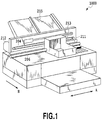
- Fig. 1 is a schematic perspective view of an inkjet printing apparatus of a first embodiment of the present invention.
- An inkjet printing apparatus 1000 shown in Fig. 1 includes a carriage 211 for mounting an inkjet print head unit 410 shown in Fig. 2A so that an ink ejection face of an inkjet print head 1 faces a print medium.
- the carriage 211 is guided and supported by a guide shaft 206 so that the carriage 211 can move in a main scan direction shown by an arrow A.
- the guide shaft 206 is disposed to extend in a width direction of a print medium.
- a belt 204 is attached to the carriage 211.
- the belt 204 is connected to a carriage motor 212 via a pulley. The driving force of the carriage motor 212 is transmitted to the carriage 211 through the belt 204, whereby the carriage 211 moves along the guide shaft 206.
- a flexible cable 213 is attached to the carriage 211.
- the flexible cable 213 is configured to be connected to the inkjet print head unit 410 in a case where the inkjet print head unit 410 is mounted in the carriage. According to print data, an electrical signal from a control unit which is not shown in the figure is transferred to the inkjet print head 1.
- a print medium is fed from a sheet feeding section 215 and conveyed by a conveyance roller which is not shown in the figure in a conveying direction, that is, a sub-scan direction shown by an arrow B.
- the inkjet printing apparatus 1000 sequentially prints an image on the print medium by repeating a printing operation of ejecting ink while moving the inkjet print head 1 in the main scan direction and a conveying operation of conveying the print medium in the sub-scan direction.
- the inkjet printing apparatus 1000 of the present embodiment is a so-called serial-scan type inkjet printing apparatus which prints an image by moving the inkjet print head 1 in the main scan direction and conveying the print medium in the sub-scan direction.
- the present invention is not limited to this, and can also be applied to a so-called full-line type inkjet printing apparatus using an inkjet print head which extends the entire width of a print medium.
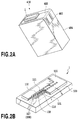
- Fig. 2A is a schematic perspective view of the inkjet print head unit of the first embodiment.
- the inkjet print head unit 410 shown in Fig. 2A is in the form of a cartridge in which the inkjet print head 1 is integral with an ink tank 404.
- the ink tank 404 temporarily stores ink therein, and supplies the ink to the inkjet print head 1.
- the inkjet print head unit 410 can be mounted in and demounted from the carriage 211 shown in Fig. 1 .
- a tape member 402 for Tape Automated Bonding (TAB) having a terminal for supplying power is attached to the inkjet print head unit 410.
- Power is selectively supplied from contacts 403 to thermal action sections 117 of the inkjet print head 1 through the tape member 402.
- TAB Tape Automated Bonding
- the inkjet print head of the present invention is not limited to the form of the above unit in which the inkjet print head is integral with the ink tank.
- the inkjet print head may be in a form that an ink tank is removably mounted and that in a case where the remaining amount of ink in the ink tank reaches zero, the ink tank is demounted and a new ink tank is mounted.
- the inkjet print head may be in a form that the inkjet print head is separate from the ink tank and that ink is supplied via a tube or the like.
- the inkjet print head of the present invention is not limited to the one applied to a serial type inkjet printing apparatus.
- the inkjet print head of the present invention may be an inkjet print head having nozzles across a region corresponding to the entire width of a print medium like the one applied to a line type inkjet printing apparatus.
- Fig. 2B is a schematic perspective view of the inkjet print head of the first embodiment.
- Fig. 2B is a partially cutaway view of the inkjet print head 1.
- a flow path forming member 120 is disposed on a substrate 100 for the inkjet print head. Between the substrate 100 for the inkjet print head and the flow path forming member 120, there are defined a plurality of liquid chambers 132 capable of storing ink therein, ink flow paths 116 which are in communication with the liquid chambers 132, and a common liquid chamber 131 which is in communication with the liquid chambers 132 via the ink flow paths.
- the substrate 100 for the inkjet print head has an ink supply port 130 penetrating the substrate 100 for the inkjet print head.
- the ink supply port 130 is disposed to correspond to the common liquid chamber 131 and is in the shape of a rectangle extending in an arrangement direction of the plurality of liquid chambers 132.
- the common liquid chamber 131 is in communication with the ink supply port 130.
- the liquid chambers 132 include the thermal action sections 117 therein. Ejection ports 121 are formed at positions corresponding to the thermal action sections 117 in the flow path forming member 120. Further, heating resistors 108 are disposed at positions corresponding to the thermal action sections 117 of the substrate 100 for the inkjet print head.
- ink is supplied from the ink tank 404 to the inkjet print head 1
- the ink is supplied to the common liquid chamber 131 through the ink supply port 130 of the substrate 100 for the inkjet print head.
- the ink supplied to the common liquid chamber 131 is supplied to the liquid chambers 132 through the ink flow paths 116.
- capillary action causes the ink in the common liquid chamber 131 to be supplied to the ink flow paths 116 and the liquid chambers 132, and a meniscus is formed at the ejection ports 121, whereby the liquid surface of ink can be stably held.
- the heating resistors 108 disposed at positions corresponding to the liquid chambers 132 are energized through wiring to generate thermal energy in the heating resistors 108.
- the ink in the liquid chambers 132 is heated and bubbles are generated by film boiling.
- the energy of the bubble generation causes ink droplets to be ejected from the ejection ports 121.
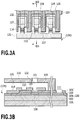
- Fig. 3A is a schematic plan view of a portion around the thermal action sections of the inkjet print head of the first embodiment of the present invention.
- Fig. 3B is a partial schematic cross-sectional view of the substrate taken along line IIIb-IIIb of Fig. 3A .
- the inkjet print head 1 comprises the substrate 100 for the inkjet print head and the flow path forming member 120 adhered to the substrate for the inkjet print head.
- a region shown as the flow path forming member 120 is a contact surface between the flow path forming member 120 and the substrate 100 for the inkjet print head.
- the substrate 100 for the inkjet print head comprises a silicon base 101.
- a heat accumulating layer 102 is disposed on the base to suppress dissipation of heat generated by the heating resistors 108.
- the heat accumulating layer 102 is made of a thermally-oxidized film, a SiO (silicon oxide) film, a SiN (silicon nitride) film, or the like.
- a heating resistor layer 104 and an electrode wiring layer 105 are disposed on the heat accumulating layer 102.
- the heating resistor layer 104 is made of resistors having the function of electrothermal conversion elements which generate heat in a case where the electrothermal conversion elements are energized.
- the electrode wiring layer 105 is made of a metal material such as A1 (aluminum), Al-Si (aluminum-silicon), or Al-Cu (aluminum-copper), and functions as electric wiring.
- the heating resistors 108 are formed by removing part of the electrode wiring layer 105 to form gaps and exposing corresponding portions of the heating resistor layer 104. More specifically, the electrode wiring layer 105 is adjacent to the heating resistor layer 104 and consists of two portions disposed with the gaps therebetween. Further, the heating resistors 108 consist only of the heating resistor layer 104. A current flows from one portion of the electrode wiring layer 105 to the other portion thereof, which are disposed separately, through the heating resistors 108, whereby the heating resistors 108 produce heat.
- the plurality of heating resistors 108 are arranged, and the ink supply port 130 extends along the arrangement direction of the heating resistors 108.
- the electrode wiring layer 105 is connected to a driving element circuit or an external power supply terminal which are not shown in the figures and can receive power from the outside.
- the electrode wiring layer 105 is disposed on the heating resistor layer 104, but it is possible to form the electrode wiring layer 105 on the base 101 or the heat accumulating layer 102, remove part of the electrode wiring layer 105 to form gaps, and dispose the heating resistor layer 104 over the electrode wiring layer 105 and the gaps.
- a protection layer 106 is disposed on the heating resistors 108 and the electrode wiring layer 105 and protects lower constituent elements below the protection layer 106 and functions as an insulating layer.
- the protection layer 106 is made of a SiO film, a SiN film, or the like.
- An upper protection layer 107 is disposed on the protection layer 106.
- the upper protection layer 107 protects the heating resistors 108 from chemical action and physical impact caused by heat of the heating resistors 108.
- the upper protection layer 107 is made of Ta (tantalum) or a platinum group element such as Ir (iridium) or Ru (ruthenium).
- the upper protection layer 107 includes a plurality of individual sections disposed to individually cover upper portions of the heating resistors 108 for the original purpose of protection and a common section 110 which connects the plurality of individual sections, and which is disposed to avoid the upper portions of the heating resistors 108.
- the individual sections of the upper protection layer 107 corresponding to the adjacent heating resistors 108 are disposed with gaps therebetween in the arrangement direction of the heating resistors 108.
- the common section 110 includes a band portion extending in the form of a band in the arrangement direction of the heating resistors 108 outside the liquid chambers 132 and a branch portion branching from the band portion into the liquid chambers 132 and connected to each individual section. Between the individual sections and the branch portion of the common section 110, there are provided thin film regions 113 in which the film thickness of the upper protection layer 107 is small. More specifically, the thin film regions 113 are connection sections which connect the common section 110 and the individual sections of the upper protection layer 107 corresponding to the heating resistors 108.
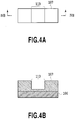
- Fig. 4A is a schematic plan view showing the thin film region 113 of the upper protection layer 107.
- Fig. 4B is a partial schematic cross-sectional view of the substrate taken along line IVb-IVb of Fig. 4A .
- the thin film region 113 of the upper protection layer is positioned in regions where ink is contacted such as the ink chambers or the ink flow paths in a case where the inkjet print head is formed.
- the upper protection layer 107 above the heating resistors 108 is formed to have a large thickness in the range of about 200 to 500 nm in order to achieve a long life.
- the thin film region 113 of the upper protection layer is formed to have a small thickness in the range of 10 to 50 nm so that in a case where a short circuit occurs, an insulating layer is formed easily in the thin film region by anodization.
- the film thickness of the thin film region 113 is preferably in the range of 10 to 30 nm.
- Fig. 5A is a circuit diagram of the first embodiment of the present invention.
- An electrical diagram of the inkjet print head 1 is substantially identical to that of the substrate 100 for the inkjet print head and will be omitted.
- a selection circuit 115 selects a switching transistor 114 provided for each of the plurality of heating resistors 108, thereby driving the plurality of heating resistors 108.
- the individual sections of the upper protection layer 107 provided to cover the upper portions of the heating resistors 108 are connected to an external electrode 111 via the thin film regions 113 and the common section 110.
- the common section 110 has the function of electric wiring.
- the external electrode 111 is grounded through an inkjet printing apparatus 300.
- a power supply 301 drives the heating resistors 108 and applies a voltage of 20 to 30 V.
- polysilicon used for a general fuse element has a melting point of about 1400°C.
- Ta used for the upper protection layer 107 is metal having a high melting point of about 4000°C.
- the upper protection layer 107 is electrically cut by using an electrochemical reaction to change the upper protection layer 107 to the insulating layer instead of melting and removing the upper protection layer 107. Accordingly, the present invention requires relatively small energy to electrically cut the upper protection layer.
- FIG. 5B A state in which a short circuit occurs will be explained with reference to Fig. 5B .
- the protection layer 106 having the function of the insulating layer is ruptured. Then, part of the upper protection layer 107 is melted and directly contacts the heating resistor layer 104, and a short circuit 200 occurs between the heating resistor layer 104 and the upper protection layer 107.
- a voltage is constantly applied to the heating resistors 108. Accordingly, in a case where the short circuit 200 occurs between the heating resistor layer 104 and the upper protection layer 107, a voltage is applied to the upper protection layer 107, and the upper protection layer 107 is at the same voltage as the heating resistors 108.
- the upper protection layer 107 is instantly anodized by an electrochemical reaction between metal forming the upper protection layer 107 and ink whose potential is lower than that of the metal, and an oxidized film is formed on a surface which is in contact with ink.
- the thin film regions 113 are provided in the connection sections of the upper protection layer 107 between the individual sections provided to cover the upper portions of the heating resistors 108 and the common section 110 connecting the individual sections.
- the film thickness of the upper protection layer 107 is small as described above. More specifically, the film thickness of the thin film regions 113 of the upper protection layer 107 is smaller than that of the individual sections of the upper protection layer 107 to cover the upper portions of the heating resistors 108.
- the film thickness of the oxidized film formed by anodization generally corresponds to the magnitude of an applied voltage.
- a voltage of 20 to 30 V is applied to one of the heating resistors 108
- an oxidized film is formed in the entire corresponding thin film region 113 of the upper protection layer 107 in the film thickness direction and the thin film region changes to the insulating layer.
- the thin film region 113 adjacent to the individual section of the upper protection layer 107 in which the short circuit occurs changes to the insulating layer. Accordingly, since the insulating layer is interposed, the individual section of the upper protection layer 107 in which the short circuit 200 occurred is electrically separated from the individual sections of the upper protection layer 107 which covers the upper portions of the other heating resistors 108.
- the upper protection layer 107 is anodized also in a case where, for example, a pinhole or the like is formed in the protection layer 106 which insulates the electrode wiring layer 105 from elements on or above the electrode wiring layer 105 at the time of manufacturing, whereby the upper protection layer 107 and the electrode wiring layer 105 are connected. Accordingly, at the time of manufacturing, it is checked whether or not the insulation properties of the protection layer 106 are ensured.
- Fig. 5C is a circuit diagram at the time of a test for checking the insulation properties of the protection layer 106.
- Checking is performed by setting up a needle (probe pin) of a prober apparatus at the external electrode 111.
- the probe pin is connected to a measurement device 302.
- the measurement device 302 has a digital or analog measurement function used for various tests for checking whether the heating resistors 108 and the switching transistors 114 function normally and the like.
- Measurement is made of a flowing current by applying a voltage between the upper protection layer 107 and the heating resistors 108 or between the upper protection layer 107 and the electrode wiring layer 105 which is equal to or higher than an actually applied voltage in a case where the print head is used. It is optimum to perform this test at the timing when the upper protection layer 107 is formed and the external electrode 111 to which electricity is applied is formed. On this occasion, since the upper protection layer 107 and the thin film regions 113 do not contact ink, an electrochemical reaction such as anodizing via ink does not occur even if a voltage is applied. Accordingly, it is possible to measure, without any problems, a leak current between the upper protection layer 107 and the heating resistors 108 and/or between the upper protection layer 107 and the electrode wiring layer 105.
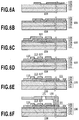
- Figs. 6A to 6F are schematic cross-sectional views for explaining the process for manufacturing the inkjet print head shown in Figs. 3A and 3B .
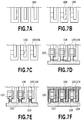
- Figs. 7A to 7E are schematic plan views for explaining the process for manufacturing the inkjet print head shown in Figs. 3A and 3B .
- the following manufacturing process is performed for the base 101 made of Si or a base into which a driving circuit having semiconductor elements such as the switching transistors 114 for selectively driving the heating resistors 108 is incorporated beforehand.
- the attached drawings show the base 101 made of Si.
- the base 101 is subjected to the thermal oxidation method, the sputtering method, the CVD method, or the like to form the heat accumulating layer 102 made of a SiO 2 thermally-oxidized film as a lower layer below the heating resistor layer 104.
- the heat accumulating layer can be formed during a process for manufacturing the driving circuit.
- the heating resistor layer 104 of TaSiN or the like is formed on the heat accumulating layer 102 by reaction sputtering so that the heating resistor layer 104 has a thickness of about 50 nm. Further, an Al layer which is to be the electrode wiring layer 105 is formed on the heating resistor layer 104 by sputtering so that the electrode wiring layer 105 has a thickness of about 300 nm. Dry etching is simultaneously performed on the heating resistor layer 104 and the electrode wiring layer 105 by the photolithography method to obtain a planar shape shown in Fig. 7A . Incidentally, in the present embodiment, the reactive ion etching (RIE) method is used as dry etching.
- RIE reactive ion etching
- wet etching is performed by using the photolithography method again to partially remove the electrode wiring layer 105 made of Al and partially expose the heating resistor layer 104 as shown in Figs. 6A and 7B .
- a SiN film as the protection layer 106 is formed to have a thickness of about 350 nm by the plasma CVD method as shown in Figs. 6B and 7C .
- a Ta layer as the upper protection layer 107 is formed on the protection layer 106 by sputtering so that the upper protection layer has a thickness of about 350 nm. Dry etching is performed by the photolithography method to partially remove the upper protection layer 107 and obtain the shape of the upper protection layer 107 as shown in Figs. 6C and 7D .
- the upper protection layer 107 includes the individual sections covering the heating resistors 108, the common section 110 connecting the individual sections, and the connection sections between the individual sections and the common section 110.
- etching is performed by the photolithography method only on the connection sections of the upper protection layer 107 between the individual sections and the common section 110 to form the thin film regions 113.
- etching is not performed on the entire upper protection layer 107 in the thickness direction and etching is stopped in a case where the thickness of the upper protection layer 107 reaches about 30 nm.
- the thin film regions 113 are formed in a shape shown in Figs. 6D and 7E .
- the thin film regions 113 are formed at positions which are to directly contact ink in a case where the inkjet print head is used.
- dry etching is performed by the photolithography method to partially remove the protection layer 106 and partially expose a corresponding portion of the electrode wiring layer 105 as shown in Fig. 6E .
- a Ta layer formed as one layer is subjected to half etching to reduce the film thickness of the thin film regions 113 as shown in Fig. 4B .
- the individual sections of the upper protection layer 107 covering the upper portions of the heating resistors 108 have a thickness of 350 nm which is large enough to achieve a long life.
- the thin film regions 113 provided in the connection sections of the upper protection layer 107 have a thickness of 30 nm.
- the power supply 301 has a voltage of 24 V and the short circuit 200 occurs, the corresponding thin film region 113 is anodized by the electrochemical reaction with ink and the entire thin film region 113 becomes a Ta oxidized film to ensure the insulation properties.
- the common section 110 needs to efficiently pass current as electric wiring, and preferably has a certain level of thickness.
- the common section 110 preferably has the same thickness (350 nm in the present embodiment) as the individual sections covering the upper portions of the heating resistors 108.
- the flow path forming member 120 is disposed on the upper side of the substrate 100 on which the upper protection layer 107 is disposed.
- the flow path forming member 120 defines the liquid chambers at the positions corresponding to the heating resistors 108 between the flow path forming member 120 and the substrate 100.
- the thin film regions 113 are disposed at the positions which are to contact ink in a case where the inkjet print head is used.
- the flow path forming member 120 is provided with the ejection ports 121 positioned to face the heating resistors 108.
- the inkjet print head of the first embodiment of the present invention is manufactured by the above process.
- the thin film regions 113 of the upper protection layer 107 are made of Ta.
- the electrochemical reaction between the upper protection layer 107 and ink forms an insulating film in the thin film region, whereby the portion in which the short circuit occurred can be electrically separated.
- This can improve the reliability of the print head with relatively small energy without requiring large energy as in the case of using fuse elements to separate the portion in which the short circuit occurred.
- the upper protection layer 107 does not reach a high temperature as in the case of using fuse elements, and accordingly, it is possible to reduce damage to nozzles.
- the corresponding thin film region 113 is anodized to become the Ta oxidized film and remains. Accordingly, even after the heater is disconnected, the protection layer 106 below the thin film region 113 can be protected from being eluted by ink.
- a positive potential may be applied to the common section 110 in a state in which the inkjet print head is filled with ink to form the insulating layer with the thin film regions 113 so that the individual sections of the upper protection layer 107 are electrically separated beforehand.
- the individual sections 107 are already electrically separated before use, there is no need to concern about sequential alteration of a large portion of the upper protection layer 107 in a case where the short circuit occurs at the time of use.
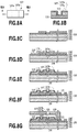
- Fig. 8A is a schematic plan view of a thin film region 113 of the second embodiment of the present invention.
- Fig. 8B is a partial schematic cross-sectional view of a substrate taken along line VIIIb-VIIIb of Fig. 8A .
- An upper protection layer 107 is divided into an upper protection layer 107a having a thickness of 300 nm and an upper protection layer 107b having a thickness of 30 nm, and both the upper protection layers 107a and 107b are formed of Ta on the heat accumulating layer 102 in the order named.
- Figs. 8C to 8G show an example of a process for manufacturing an inkjet print head of the second embodiment.
- Fig. 8C is identical to Fig. 6B for explaining the first embodiment. Steps performed to reach a state shown in Fig. 8C are identical to those of the first embodiment.
- a Ta layer having a thickness of about 300 nm as the upper protection layer 107a is formed by sputtering on a protection layer 106 of a substrate 100 in a state shown in Fig. 8C . Dry etching is performed by the photolithography method to partially remove the upper protection layer 107a and obtain the shape of the upper protection layer 107a shown in Fig. 8D . At this stage, the upper protection layer does not exist in a portion corresponding to the thin film region 113.
- a Ta layer having a thickness of about 30 nm as the upper protection layer 107b is formed by sputtering on an upper surface of the upper protection layer 107a. Then dry etching is performed by the photolithography method to partially remove the upper protection layer 107b and obtain the shape of the upper protection layer 107b shown in Fig. 8E .
- This upper protection layer 107b covers the previously formed upper protection layer 107a.
- Fig. 8A which is a plan view
- the upper protection layer 107b protrudes outward from the upper protection layer 107a.
- the upper protection layer 107b is also provided in the above-described portion corresponding to the thin film region 113 from which the upper protection layer 107a is removed.
- the thin film region 113 of the upper protection layer 107 is made of Ta. According to this feature, an electrochemical reaction between the upper protection layer 107 and ink forms the insulation film in the thin film region, whereby a portion in which a short circuit occurred can be electrically separated.
- the film thickness of the thin film region 113 is determined based only on a condition of sputtering for the upper protection layer 107b, and it is easy to improve the precision of the film thickness of the thin film region 113.
- a third embodiment of the present invention will be specifically explained with reference to Figs. 9A to 9G . Explanation of features similar to those of the first embodiment will be omitted.
- Fig. 9A is a schematic plan view of a thin film region 113 of an upper protection layer 107 of the third embodiment of the present invention.
- Fig. 9B is a partial schematic cross-sectional view of a substrate taken along line IXb-IXb of Fig. 9A .
- the upper protection layer 107 is divided into an upper protection layer 107c having a thickness of 50 nm and an upper protection layer 107d having a thickness of 250 nm and the upper protection layers 107c and 107d are formed on a heat accumulating layer 102 in the order named.
- the upper protection layer 107c is made of Ta
- the upper protection layer 107d is made of platinum group metal Ir.
- the upper protection layer 107c and the upper protection layer 107d are formed in substantially identical patterns. In the thin film region 113, the upper protection layer 107d is removed and only the upper protection layer 107c exists.
- Figs. 9C to 9E show an example of a process for manufacturing an inkjet print head of the third embodiment.
- Fig. 9C is identical to Fig. 6B for explaining the first embodiment, and steps performed to reach a state shown in Fig. 9C are identical to those of the first embodiment.
- a Ta layer having a thickness of about 50 nm as the upper protection layer 107c is formed by sputtering on a protection layer 106 of a substrate 100 in a state shown in Fig. 9C .
- an Ir layer having a thickness of about 250 nm is formed by sputtering as the upper protection layer 107d.
- dry etching is performed by the photolithography method to remove a portion corresponding to the thin film region 113 of the upper protection layer 107d and obtain the shape of the upper protection layer 107d shown in Fig. 9D .
- Dry etching is performed by the photolithography method to partially remove the upper protection layer 107c and obtain the shape of the upper protection layer 107c shown in Fig. 9E .
- Fig. 9A which is a plan view
- a region in which the upper protection layer 107d is disposed is within a region in which the upper protection layer 107c is disposed. Further, the upper protection layer 107d does not exist in the thin film region 113.
- Both Ir used for the upper protection layer 107d and Ta used for the upper protection layer 107c are generally suitably used as materials for protecting heating resistors of the inkjet print head. These materials have conductivity.
- the upper protection layer 107 causes an electrochemical reaction with ink as an electrolyte solution
- the constituent material is Ir
- Ir itself as a metal ion is eluted in ink
- the constituent material is Ta
- the upper protection layer 107 is anodized to form an oxidized film.
- the thin film region 113 of the upper protection layer 107 is made of Ta.
- an electrochemical reaction between the upper protection layer 107 and ink forms an insulation film in the thin film region 113, whereby a portion in which a short circuit occurred can be electrically separated.
- Ir does not adhere tightly to SiN forming the protection layer 106. Further, Ir is a platinum group element and etching is generally performed by a more physical method. In this case, there is a possibility that SiN forming a foundation is also etched at a high speed, and that the function of the protection layer 106 is damaged.
- Ta for the upper protection layer 107c interposed between the upper protection layer 107d and the protection layer 106 has the function of improving adhesiveness between these layers.
- the upper protection layer 107c made of Ta and the upper protection layer 107d made of Ir are provided on the protection layer 106 in the order named, it is easy to control etching at the time of manufacturing, and adhesiveness between the layers is high.
- Ta is used as a material for the thin film region 113 of the upper protection layer.
- the present invention is not limited to this, and a material (such as Ta, Cr, Ni, or an alloy thereof) which changes to an insulation film as a result of an electrochemical reaction with ink can be used for the thin film region 113.
- Ir is used as a material for the upper protection layer 107d.
- the present invention is not limited to this, and another platinum group element may be used for the upper protection layer 107d in place of Ir.
- the two upper protection layers are formed.
- the present invention is not limited to this, and three or more upper protection layers may be formed.
- the number of materials for the upper protection layers may be one and may be two or more as long as the material(s) which change(s) to the insulation film as a result of an electrochemical reaction with ink is (are) used for the thin film region 113.
Description
- The present invention relates to a substrate for an inkjet print head for conducting printing on a print medium by ejecting ink according to an inkjet method, an inkjet print head having the substrate, a method for manufacturing the inkjet print head, and an inkjet printing apparatus.
- There is conventionally known an inkjet print head including liquid chambers and heating resistors near the liquid chambers wherein film boiling is caused in ink in the liquid chamber by heat generated by energizing the heating resistors, and the energy of a generated bubble causes the ink in the liquid chamber to be ejected.
- At the time of printing, the heating resistors of the above inkjet print head are occasionally affected by physical action such as the impact of cavitation caused by bubble generation, shrinkage, and disappearing in ink and/or the chemical action of ink. In order to protect the heating resistors from the physical action and the chemical action, an upper protection layer is disposed to cover upper portions of the heating resistors.
- This upper protection layer is disposed at a position to be in contact with ink. Further, since the upper protection layer is formed above the upper portions of the heating resistors, the temperature of the upper protection layer rises instantly. In such a severe environment, the upper protection layer is normally likely to corrode. Accordingly, the upper protection layer is formed with a material which has excellent resistance to the physical action and the chemical action such as impact resistance, heat resistance, and corrosion resistance. More specifically, the upper protection layer is formed with a metal film of Ta (tantalum), a platinum group element Ir (iridium) or Ru (ruthenium), or the like satisfying the above conditions.
- Incidentally, these materials are conductive. In a case where a current flows through the upper protection layer, an electrochemical reaction occasionally occurs between the upper protection layer and ink, thereby damaging the function of the upper protection layer. In order to prevent this, an insulating layer (a protection layer having electrical insulation properties) is disposed between the heating resistors and the upper protection layer so that a current supplied to the heating resistors does not flow through the upper protection layer.
- In such a configuration, there is a case where a short circuit occurs for some reason and a current directly flows from the heating resistors or wiring connected thereto to the upper protection layer. In a case where the short circuit causes the current to flow through the upper protection layer, an electrochemical reaction between the upper protection layer and ink occasionally occurs in a region through which the current flows, thereby degenerating the upper protection layer.
- In order to prevent the short circuit from degenerating a large portion of the upper protection layer, it is considered effective to provide the upper protection layer such that in a case where the short circuit occurs, the region of the upper protection layer in which the short circuit occurs can be electrically separated from the other region.
-
Japanese Patent Laid-Open No. 2001-080073 -
EP 1 352 744 A2 - In such a configuration, the upper protection layer needs to serve two roles. One of the roles is to protect lower constituent elements below the upper protection layer from the physical action and the chemical action, and this role is the original role of the upper protection layer. In order to serve this role, the upper protection layer needs to have a certain level of thickness. The other role is to form part of the upper protection layer to be the fuse elements and in a case where one of the heating resistors is damaged, blow the corresponding fuse element. Since high-melting-point metal such as Ta or a platinum group element is used for the upper protection layer, large energy is necessary to blow the fuse elements. Accordingly, in order to achieve this role, it is desirable that the upper protection layer be as thin as possible. In other words, there is a problem that the two roles have contradictory requirements for a film thickness. For example, there is a concern that in a case where the upper protection layer is designed to be thick to achieve the long life of the print head, it becomes difficult to blow the fuse elements and the reliability of the inkjet print head is lowered.
- Therefore, an object of the present invention is to provide an inkjet print head having both long life and high reliability. Further, another object of the present invention is to provide a method for manufacturing the inkjet print head, a substrate for the inkjet print head, and an inkjet printing apparatus.
- According to the present invention which solves the above problem, there is provided a substrate for an inkjet print head comprising: a base; a plurality of heating resistors for heating ink, the heating resistors being disposed on the base and producing heat in a case where the heating resistors are energized; a first protection layer disposed on the heating resistors and having electrical insulation properties; and a second protection layer disposed on the first protection layer and having conductivity, wherein the second protection layer includes individual sections disposed to individually cover the plurality of heating resistors, a common section connecting the individual sections, and connection sections interposed between the individual sections and the common section and connecting the individual sections and the common section, and the connection sections are disposed at positions to be in contact with ink, and include a material which changes to an electrically insulating film by an electrochemical reaction with the ink.
- In the configuration of the present invention, in a case where a short circuit occurs in the upper protection layer, an electrochemical reaction between the upper protection layer and ink forms an insulating layer in the connection sections connecting the individual sections and the common section. This enables a region of the upper protection layer in which the short circuit occurs to be separated from the other regions. The present invention can separate the region of the upper protection layer in which the short circuit occurs from the other regions without requiring large energy for blowing fuse elements. Further, according to the present invention, in a case where the upper protection layer is separated, the upper protection layer does not reach a high temperature like the one in a case where fuse elements are blown. Accordingly, damage to nozzles can be reduced.
- Further features of the present invention will become apparent from the following description of exemplary embodiments (with reference to the attached drawings).
-
-
Fig. 1 is a schematic perspective view of an inkjet printing apparatus of a first embodiment; -
Fig. 2A is a schematic perspective view of an inkjet print head unit of the first embodiment; -
Fig. 2B is a schematic perspective view of an inkjet print head of the first embodiment; -
Fig. 3A is a schematic plan view of a portion around thermal action sections of a substrate for the inkjet print head of the first embodiment; -
Fig. 3B is a cross-sectional view of the portion around the thermal action sections of the substrate for the inkjet print head of the first embodiment; -
Fig. 4A is a plan view of a thin film region of an upper protection layer of the first embodiment; -
Fig. 4B is a schematic cross-sectional view of the thin film region of the upper protection layer of the first embodiment; -
Figs. 5A to 5C are circuit diagrams of the first embodiment; -
Figs. 6A to 6F are schematic cross-sectional views for explaining a process for manufacturing the inkjet print head of the first embodiment; -
Figs. 7A to 7F are schematic plan views for explaining the process for manufacturing the inkjet print head of the first embodiment; -
Figs. 8A and 8B are schematic views of a thin film region of an upper protection layer of a second embodiment; -
Figs. 8C to 8G are views for explaining a process for manufacturing the thin film region of the upper protection layer of the second embodiment; -
Figs. 9A and 9B are schematic views of a thin film region of an upper protection layer of a third embodiment; and -
Figs. 9C to 9G are views for explaining a process for manufacturing the thin film region of the upper protection layer of the third embodiment. - With reference to the drawings, explanation will be made below on an inkjet printing apparatus, an inkjet print head, and a substrate for the inkjet print head according to embodiments of the present invention.
-
Fig. 1 is a schematic perspective view of an inkjet printing apparatus of a first embodiment of the present invention. Aninkjet printing apparatus 1000 shown inFig. 1 includes acarriage 211 for mounting an inkjetprint head unit 410 shown inFig. 2A so that an ink ejection face of aninkjet print head 1 faces a print medium. - The
carriage 211 is guided and supported by aguide shaft 206 so that thecarriage 211 can move in a main scan direction shown by an arrow A. Theguide shaft 206 is disposed to extend in a width direction of a print medium. Abelt 204 is attached to thecarriage 211. Thebelt 204 is connected to acarriage motor 212 via a pulley. The driving force of thecarriage motor 212 is transmitted to thecarriage 211 through thebelt 204, whereby thecarriage 211 moves along theguide shaft 206. - A
flexible cable 213 is attached to thecarriage 211. Theflexible cable 213 is configured to be connected to the inkjetprint head unit 410 in a case where the inkjetprint head unit 410 is mounted in the carriage. According to print data, an electrical signal from a control unit which is not shown in the figure is transferred to theinkjet print head 1. - A print medium is fed from a
sheet feeding section 215 and conveyed by a conveyance roller which is not shown in the figure in a conveying direction, that is, a sub-scan direction shown by an arrow B. - The
inkjet printing apparatus 1000 sequentially prints an image on the print medium by repeating a printing operation of ejecting ink while moving theinkjet print head 1 in the main scan direction and a conveying operation of conveying the print medium in the sub-scan direction. - As described above, the
inkjet printing apparatus 1000 of the present embodiment is a so-called serial-scan type inkjet printing apparatus which prints an image by moving theinkjet print head 1 in the main scan direction and conveying the print medium in the sub-scan direction. Incidentally, the present invention is not limited to this, and can also be applied to a so-called full-line type inkjet printing apparatus using an inkjet print head which extends the entire width of a print medium. -
Fig. 2A is a schematic perspective view of the inkjet print head unit of the first embodiment. The inkjetprint head unit 410 shown inFig. 2A is in the form of a cartridge in which theinkjet print head 1 is integral with anink tank 404. Theink tank 404 temporarily stores ink therein, and supplies the ink to theinkjet print head 1. - The inkjet
print head unit 410 can be mounted in and demounted from thecarriage 211 shown inFig. 1 . Atape member 402 for Tape Automated Bonding (TAB) having a terminal for supplying power is attached to the inkjetprint head unit 410. Power is selectively supplied fromcontacts 403 tothermal action sections 117 of theinkjet print head 1 through thetape member 402. - Incidentally, the inkjet print head of the present invention is not limited to the form of the above unit in which the inkjet print head is integral with the ink tank. For example, the inkjet print head may be in a form that an ink tank is removably mounted and that in a case where the remaining amount of ink in the ink tank reaches zero, the ink tank is demounted and a new ink tank is mounted. Further, the inkjet print head may be in a form that the inkjet print head is separate from the ink tank and that ink is supplied via a tube or the like.
- Further, the inkjet print head of the present invention is not limited to the one applied to a serial type inkjet printing apparatus. The inkjet print head of the present invention may be an inkjet print head having nozzles across a region corresponding to the entire width of a print medium like the one applied to a line type inkjet printing apparatus.
-
Fig. 2B is a schematic perspective view of the inkjet print head of the first embodiment.Fig. 2B is a partially cutaway view of theinkjet print head 1. - In the
inkjet print head 1 of the present embodiment, a flowpath forming member 120 is disposed on asubstrate 100 for the inkjet print head. Between thesubstrate 100 for the inkjet print head and the flowpath forming member 120, there are defined a plurality ofliquid chambers 132 capable of storing ink therein,ink flow paths 116 which are in communication with theliquid chambers 132, and acommon liquid chamber 131 which is in communication with theliquid chambers 132 via the ink flow paths. Thesubstrate 100 for the inkjet print head has anink supply port 130 penetrating thesubstrate 100 for the inkjet print head. Theink supply port 130 is disposed to correspond to thecommon liquid chamber 131 and is in the shape of a rectangle extending in an arrangement direction of the plurality ofliquid chambers 132. Thecommon liquid chamber 131 is in communication with theink supply port 130. - The
liquid chambers 132 include thethermal action sections 117 therein.Ejection ports 121 are formed at positions corresponding to thethermal action sections 117 in the flowpath forming member 120. Further,heating resistors 108 are disposed at positions corresponding to thethermal action sections 117 of thesubstrate 100 for the inkjet print head. - In a case where ink is supplied from the
ink tank 404 to theinkjet print head 1, the ink is supplied to thecommon liquid chamber 131 through theink supply port 130 of thesubstrate 100 for the inkjet print head. The ink supplied to thecommon liquid chamber 131 is supplied to theliquid chambers 132 through theink flow paths 116. On this occasion, capillary action causes the ink in thecommon liquid chamber 131 to be supplied to theink flow paths 116 and theliquid chambers 132, and a meniscus is formed at theejection ports 121, whereby the liquid surface of ink can be stably held. - In order to eject ink, the
heating resistors 108 disposed at positions corresponding to theliquid chambers 132 are energized through wiring to generate thermal energy in theheating resistors 108. As a result, the ink in theliquid chambers 132 is heated and bubbles are generated by film boiling. The energy of the bubble generation causes ink droplets to be ejected from theejection ports 121. -
Fig. 3A is a schematic plan view of a portion around the thermal action sections of the inkjet print head of the first embodiment of the present invention.Fig. 3B is a partial schematic cross-sectional view of the substrate taken along line IIIb-IIIb ofFig. 3A . - The
inkjet print head 1, part of which is schematically shown inFigs. 3A and 3B , comprises thesubstrate 100 for the inkjet print head and the flowpath forming member 120 adhered to the substrate for the inkjet print head. InFig. 3A which is a plan view, a region shown as the flowpath forming member 120 is a contact surface between the flowpath forming member 120 and thesubstrate 100 for the inkjet print head. - The
substrate 100 for the inkjet print head comprises asilicon base 101. Aheat accumulating layer 102 is disposed on the base to suppress dissipation of heat generated by theheating resistors 108. Theheat accumulating layer 102 is made of a thermally-oxidized film, a SiO (silicon oxide) film, a SiN (silicon nitride) film, or the like. - A
heating resistor layer 104 and anelectrode wiring layer 105 are disposed on theheat accumulating layer 102. Theheating resistor layer 104 is made of resistors having the function of electrothermal conversion elements which generate heat in a case where the electrothermal conversion elements are energized. Theelectrode wiring layer 105 is made of a metal material such as A1 (aluminum), Al-Si (aluminum-silicon), or Al-Cu (aluminum-copper), and functions as electric wiring. - The
heating resistors 108 are formed by removing part of theelectrode wiring layer 105 to form gaps and exposing corresponding portions of theheating resistor layer 104. More specifically, theelectrode wiring layer 105 is adjacent to theheating resistor layer 104 and consists of two portions disposed with the gaps therebetween. Further, theheating resistors 108 consist only of theheating resistor layer 104. A current flows from one portion of theelectrode wiring layer 105 to the other portion thereof, which are disposed separately, through theheating resistors 108, whereby theheating resistors 108 produce heat. The plurality ofheating resistors 108 are arranged, and theink supply port 130 extends along the arrangement direction of theheating resistors 108. - The
electrode wiring layer 105 is connected to a driving element circuit or an external power supply terminal which are not shown in the figures and can receive power from the outside. In the embodiment shown in the figures, theelectrode wiring layer 105 is disposed on theheating resistor layer 104, but it is possible to form theelectrode wiring layer 105 on the base 101 or theheat accumulating layer 102, remove part of theelectrode wiring layer 105 to form gaps, and dispose theheating resistor layer 104 over theelectrode wiring layer 105 and the gaps. - A
protection layer 106 is disposed on theheating resistors 108 and theelectrode wiring layer 105 and protects lower constituent elements below theprotection layer 106 and functions as an insulating layer. Theprotection layer 106 is made of a SiO film, a SiN film, or the like. - An
upper protection layer 107 is disposed on theprotection layer 106. Theupper protection layer 107 protects theheating resistors 108 from chemical action and physical impact caused by heat of theheating resistors 108. In the present embodiment, theupper protection layer 107 is made of Ta (tantalum) or a platinum group element such as Ir (iridium) or Ru (ruthenium). - The
upper protection layer 107 includes a plurality of individual sections disposed to individually cover upper portions of theheating resistors 108 for the original purpose of protection and acommon section 110 which connects the plurality of individual sections, and which is disposed to avoid the upper portions of theheating resistors 108. - With reference to
Fig. 3A , in the present embodiment, the individual sections of theupper protection layer 107 corresponding to theadjacent heating resistors 108 are disposed with gaps therebetween in the arrangement direction of theheating resistors 108. Thecommon section 110 includes a band portion extending in the form of a band in the arrangement direction of theheating resistors 108 outside theliquid chambers 132 and a branch portion branching from the band portion into theliquid chambers 132 and connected to each individual section. Between the individual sections and the branch portion of thecommon section 110, there are providedthin film regions 113 in which the film thickness of theupper protection layer 107 is small. More specifically, thethin film regions 113 are connection sections which connect thecommon section 110 and the individual sections of theupper protection layer 107 corresponding to theheating resistors 108. -
Fig. 4A is a schematic plan view showing thethin film region 113 of theupper protection layer 107.Fig. 4B is a partial schematic cross-sectional view of the substrate taken along line IVb-IVb ofFig. 4A . Thethin film region 113 of the upper protection layer is positioned in regions where ink is contacted such as the ink chambers or the ink flow paths in a case where the inkjet print head is formed. Theupper protection layer 107 above theheating resistors 108 is formed to have a large thickness in the range of about 200 to 500 nm in order to achieve a long life. Further, thethin film region 113 of the upper protection layer is formed to have a small thickness in the range of 10 to 50 nm so that in a case where a short circuit occurs, an insulating layer is formed easily in the thin film region by anodization. The film thickness of thethin film region 113 is preferably in the range of 10 to 30 nm. -
Fig. 5A is a circuit diagram of the first embodiment of the present invention. An electrical diagram of theinkjet print head 1 is substantially identical to that of thesubstrate 100 for the inkjet print head and will be omitted. Aselection circuit 115 selects a switchingtransistor 114 provided for each of the plurality ofheating resistors 108, thereby driving the plurality ofheating resistors 108. The individual sections of theupper protection layer 107 provided to cover the upper portions of theheating resistors 108 are connected to anexternal electrode 111 via thethin film regions 113 and thecommon section 110. Thecommon section 110 has the function of electric wiring. Theexternal electrode 111 is grounded through aninkjet printing apparatus 300. Apower supply 301 drives theheating resistors 108 and applies a voltage of 20 to 30 V. - Incidentally, polysilicon used for a general fuse element has a melting point of about 1400°C. In contrast, Ta used for the
upper protection layer 107 is metal having a high melting point of about 4000°C. In order to blow the fuse element, it is necessary to melt and remove at least a certain volume of a material forming the fuse element. Accordingly, in a case where the fuse element is formed with Ta, large energy is necessary to blow or melt the fuse element. However, according to the present invention, theupper protection layer 107 is electrically cut by using an electrochemical reaction to change theupper protection layer 107 to the insulating layer instead of melting and removing theupper protection layer 107. Accordingly, the present invention requires relatively small energy to electrically cut the upper protection layer. - A state in which a short circuit occurs will be explained with reference to
Fig. 5B . In a case where one of theheating resistors 108 is damaged, theprotection layer 106 having the function of the insulating layer is ruptured. Then, part of theupper protection layer 107 is melted and directly contacts theheating resistor layer 104, and ashort circuit 200 occurs between theheating resistor layer 104 and theupper protection layer 107. A voltage is constantly applied to theheating resistors 108. Accordingly, in a case where theshort circuit 200 occurs between theheating resistor layer 104 and theupper protection layer 107, a voltage is applied to theupper protection layer 107, and theupper protection layer 107 is at the same voltage as theheating resistors 108. In a case where theheating resistors 108 are driven at a positive voltage, theupper protection layer 107 is instantly anodized by an electrochemical reaction between metal forming theupper protection layer 107 and ink whose potential is lower than that of the metal, and an oxidized film is formed on a surface which is in contact with ink. - According to the present invention, the
thin film regions 113 are provided in the connection sections of theupper protection layer 107 between the individual sections provided to cover the upper portions of theheating resistors 108 and thecommon section 110 connecting the individual sections. In thethin film regions 113 of the present invention, the film thickness of theupper protection layer 107 is small as described above. More specifically, the film thickness of thethin film regions 113 of theupper protection layer 107 is smaller than that of the individual sections of theupper protection layer 107 to cover the upper portions of theheating resistors 108. - The film thickness of the oxidized film formed by anodization generally corresponds to the magnitude of an applied voltage. In a case where a voltage of 20 to 30 V is applied to one of the
heating resistors 108, an oxidized film is formed in the entire correspondingthin film region 113 of theupper protection layer 107 in the film thickness direction and the thin film region changes to the insulating layer. In other words, in a case where theshort circuit 200 occurs, thethin film region 113 adjacent to the individual section of theupper protection layer 107 in which the short circuit occurs changes to the insulating layer. Accordingly, since the insulating layer is interposed, the individual section of theupper protection layer 107 in which theshort circuit 200 occurred is electrically separated from the individual sections of theupper protection layer 107 which covers the upper portions of theother heating resistors 108. - Therefore, the
thin film regions 113 of the present invention interposed between the individual sections and thecommon section 110 of theupper protection layer 107 play a large role in achieving the long life of the entire substrate for inkjet printing. - The
upper protection layer 107 is anodized also in a case where, for example, a pinhole or the like is formed in theprotection layer 106 which insulates theelectrode wiring layer 105 from elements on or above theelectrode wiring layer 105 at the time of manufacturing, whereby theupper protection layer 107 and theelectrode wiring layer 105 are connected. Accordingly, at the time of manufacturing, it is checked whether or not the insulation properties of theprotection layer 106 are ensured. - With reference to
Fig. 5C , a test for checking the insulation properties of theprotection layer 106 will be explained below.Fig. 5C is a circuit diagram at the time of a test for checking the insulation properties of theprotection layer 106. Checking is performed by setting up a needle (probe pin) of a prober apparatus at theexternal electrode 111. The probe pin is connected to ameasurement device 302. Themeasurement device 302 has a digital or analog measurement function used for various tests for checking whether theheating resistors 108 and the switchingtransistors 114 function normally and the like. Measurement is made of a flowing current by applying a voltage between theupper protection layer 107 and theheating resistors 108 or between theupper protection layer 107 and theelectrode wiring layer 105 which is equal to or higher than an actually applied voltage in a case where the print head is used. It is optimum to perform this test at the timing when theupper protection layer 107 is formed and theexternal electrode 111 to which electricity is applied is formed. On this occasion, since theupper protection layer 107 and thethin film regions 113 do not contact ink, an electrochemical reaction such as anodizing via ink does not occur even if a voltage is applied. Accordingly, it is possible to measure, without any problems, a leak current between theupper protection layer 107 and theheating resistors 108 and/or between theupper protection layer 107 and theelectrode wiring layer 105. - Explanation will be made below on an example of a process for manufacturing the inkjet print head of the first embodiment.
Figs. 6A to 6F are schematic cross-sectional views for explaining the process for manufacturing the inkjet print head shown inFigs. 3A and 3B . Further,Figs. 7A to 7E are schematic plan views for explaining the process for manufacturing the inkjet print head shown inFigs. 3A and 3B . - The following manufacturing process is performed for the base 101 made of Si or a base into which a driving circuit having semiconductor elements such as the switching
transistors 114 for selectively driving theheating resistors 108 is incorporated beforehand. For sake of simplification of explanation, the attached drawings show the base 101 made of Si. - First, with reference to
Fig. 6A , thebase 101 is subjected to the thermal oxidation method, the sputtering method, the CVD method, or the like to form theheat accumulating layer 102 made of a SiO2 thermally-oxidized film as a lower layer below theheating resistor layer 104. Incidentally, regarding the base into which the driving circuit is incorporated beforehand, the heat accumulating layer can be formed during a process for manufacturing the driving circuit. - Next, with reference to
Fig. 6A , theheating resistor layer 104 of TaSiN or the like is formed on theheat accumulating layer 102 by reaction sputtering so that theheating resistor layer 104 has a thickness of about 50 nm. Further, an Al layer which is to be theelectrode wiring layer 105 is formed on theheating resistor layer 104 by sputtering so that theelectrode wiring layer 105 has a thickness of about 300 nm. Dry etching is simultaneously performed on theheating resistor layer 104 and theelectrode wiring layer 105 by the photolithography method to obtain a planar shape shown inFig. 7A . Incidentally, in the present embodiment, the reactive ion etching (RIE) method is used as dry etching. - Next, in order to form the
heating resistors 108, wet etching is performed by using the photolithography method again to partially remove theelectrode wiring layer 105 made of Al and partially expose theheating resistor layer 104 as shown inFigs. 6A and7B . Incidentally, in order to achieve the excellent coverage properties of theprotect layer 106 at wiring ends, it is desirable to perform publicly-known wet etching for obtaining an appropriate tapered shape at the wiring ends. - Thereafter, a SiN film as the
protection layer 106 is formed to have a thickness of about 350 nm by the plasma CVD method as shown inFigs. 6B and7C . - Next, a Ta layer as the
upper protection layer 107 is formed on theprotection layer 106 by sputtering so that the upper protection layer has a thickness of about 350 nm. Dry etching is performed by the photolithography method to partially remove theupper protection layer 107 and obtain the shape of theupper protection layer 107 as shown inFigs. 6C and7D . In this stage, theupper protection layer 107 includes the individual sections covering theheating resistors 108, thecommon section 110 connecting the individual sections, and the connection sections between the individual sections and thecommon section 110. - Next, dry etching is performed by the photolithography method only on the connection sections of the
upper protection layer 107 between the individual sections and thecommon section 110 to form thethin film regions 113. On this occasion, etching is not performed on the entireupper protection layer 107 in the thickness direction and etching is stopped in a case where the thickness of theupper protection layer 107 reaches about 30 nm. Thethin film regions 113 are formed in a shape shown inFigs. 6D and7E . Thethin film regions 113 are formed at positions which are to directly contact ink in a case where the inkjet print head is used. - Next, in order to form the
external electrode 111, dry etching is performed by the photolithography method to partially remove theprotection layer 106 and partially expose a corresponding portion of theelectrode wiring layer 105 as shown inFig. 6E . - In the present embodiment, a Ta layer formed as one layer is subjected to half etching to reduce the film thickness of the
thin film regions 113 as shown inFig. 4B . The individual sections of theupper protection layer 107 covering the upper portions of theheating resistors 108 have a thickness of 350 nm which is large enough to achieve a long life. In contrast, thethin film regions 113 provided in the connection sections of theupper protection layer 107 have a thickness of 30 nm. In a case where thepower supply 301 has a voltage of 24 V and theshort circuit 200 occurs, the correspondingthin film region 113 is anodized by the electrochemical reaction with ink and the entirethin film region 113 becomes a Ta oxidized film to ensure the insulation properties. - On this occasion, only the
thin film regions 113 may be thin or the entirecommon section 110 may also be formed to be a thin film. However, thecommon section 110 needs to efficiently pass current as electric wiring, and preferably has a certain level of thickness. For example, thecommon section 110 preferably has the same thickness (350 nm in the present embodiment) as the individual sections covering the upper portions of theheating resistors 108. - Next, with reference to
Fig. 6F , the flowpath forming member 120 is disposed on the upper side of thesubstrate 100 on which theupper protection layer 107 is disposed. The flowpath forming member 120 defines the liquid chambers at the positions corresponding to theheating resistors 108 between the flowpath forming member 120 and thesubstrate 100. Thethin film regions 113 are disposed at the positions which are to contact ink in a case where the inkjet print head is used. Further, the flowpath forming member 120 is provided with theejection ports 121 positioned to face theheating resistors 108. - The inkjet print head of the first embodiment of the present invention is manufactured by the above process.
- According to the features of the present embodiment, the
thin film regions 113 of theupper protection layer 107 are made of Ta. The electrochemical reaction between theupper protection layer 107 and ink forms an insulating film in the thin film region, whereby the portion in which the short circuit occurred can be electrically separated. This can improve the reliability of the print head with relatively small energy without requiring large energy as in the case of using fuse elements to separate the portion in which the short circuit occurred. Further, in a case where the portion in which the short circuit occurred is separated, theupper protection layer 107 does not reach a high temperature as in the case of using fuse elements, and accordingly, it is possible to reduce damage to nozzles. - According to the above features, after one of the heating resistors 108 (heaters) is disconnected, the corresponding
thin film region 113 is anodized to become the Ta oxidized film and remains. Accordingly, even after the heater is disconnected, theprotection layer 106 below thethin film region 113 can be protected from being eluted by ink. - In the above features, after a test for checking the insulation properties of the above protection layer and before shipment, a positive potential may be applied to the
common section 110 in a state in which the inkjet print head is filled with ink to form the insulating layer with thethin film regions 113 so that the individual sections of theupper protection layer 107 are electrically separated beforehand. In this case, since theindividual sections 107 are already electrically separated before use, there is no need to concern about sequential alteration of a large portion of theupper protection layer 107 in a case where the short circuit occurs at the time of use. - A second embodiment of the present invention will be specifically explained below with reference to
Figs. 8A to 8G . Explanation of features similar to those of the first embodiment will be omitted. -
Fig. 8A is a schematic plan view of athin film region 113 of the second embodiment of the present invention.Fig. 8B is a partial schematic cross-sectional view of a substrate taken along line VIIIb-VIIIb ofFig. 8A . Anupper protection layer 107 is divided into anupper protection layer 107a having a thickness of 300 nm and anupper protection layer 107b having a thickness of 30 nm, and both theupper protection layers heat accumulating layer 102 in the order named. -
Figs. 8C to 8G show an example of a process for manufacturing an inkjet print head of the second embodiment.Fig. 8C is identical toFig. 6B for explaining the first embodiment. Steps performed to reach a state shown inFig. 8C are identical to those of the first embodiment. - A Ta layer having a thickness of about 300 nm as the
upper protection layer 107a is formed by sputtering on aprotection layer 106 of asubstrate 100 in a state shown inFig. 8C . Dry etching is performed by the photolithography method to partially remove theupper protection layer 107a and obtain the shape of theupper protection layer 107a shown inFig. 8D . At this stage, the upper protection layer does not exist in a portion corresponding to thethin film region 113. - Next, a Ta layer having a thickness of about 30 nm as the
upper protection layer 107b is formed by sputtering on an upper surface of theupper protection layer 107a. Then dry etching is performed by the photolithography method to partially remove theupper protection layer 107b and obtain the shape of theupper protection layer 107b shown inFig. 8E . Thisupper protection layer 107b covers the previously formedupper protection layer 107a. With reference toFig. 8A which is a plan view, theupper protection layer 107b protrudes outward from theupper protection layer 107a. Theupper protection layer 107b is also provided in the above-described portion corresponding to thethin film region 113 from which theupper protection layer 107a is removed. - Accordingly, in the present embodiment, the
thin film region 113 of theupper protection layer 107 is made of Ta. According to this feature, an electrochemical reaction between theupper protection layer 107 and ink forms the insulation film in the thin film region, whereby a portion in which a short circuit occurred can be electrically separated. - Subsequent steps shown in
Figs. 8F and 8G are identical to those of the first embodiment shown inFigs. 6E and 6F . - In the present embodiment, the film thickness of the
thin film region 113 is determined based only on a condition of sputtering for theupper protection layer 107b, and it is easy to improve the precision of the film thickness of thethin film region 113. - A third embodiment of the present invention will be specifically explained with reference to
Figs. 9A to 9G . Explanation of features similar to those of the first embodiment will be omitted. -
Fig. 9A is a schematic plan view of athin film region 113 of anupper protection layer 107 of the third embodiment of the present invention.Fig. 9B is a partial schematic cross-sectional view of a substrate taken along line IXb-IXb ofFig. 9A . Theupper protection layer 107 is divided into anupper protection layer 107c having a thickness of 50 nm and anupper protection layer 107d having a thickness of 250 nm and the upper protection layers 107c and 107d are formed on aheat accumulating layer 102 in the order named. Theupper protection layer 107c is made of Ta, and theupper protection layer 107d is made of platinum group metal Ir. - The
upper protection layer 107c and theupper protection layer 107d are formed in substantially identical patterns. In thethin film region 113, theupper protection layer 107d is removed and only theupper protection layer 107c exists. -
Figs. 9C to 9E show an example of a process for manufacturing an inkjet print head of the third embodiment.Fig. 9C is identical toFig. 6B for explaining the first embodiment, and steps performed to reach a state shown inFig. 9C are identical to those of the first embodiment. - A Ta layer having a thickness of about 50 nm as the
upper protection layer 107c is formed by sputtering on aprotection layer 106 of asubstrate 100 in a state shown inFig. 9C . Then an Ir layer having a thickness of about 250 nm is formed by sputtering as theupper protection layer 107d. Next, dry etching is performed by the photolithography method to remove a portion corresponding to thethin film region 113 of theupper protection layer 107d and obtain the shape of theupper protection layer 107d shown inFig. 9D . - Dry etching is performed by the photolithography method to partially remove the
upper protection layer 107c and obtain the shape of theupper protection layer 107c shown inFig. 9E . With reference toFig. 9A which is a plan view, a region in which theupper protection layer 107d is disposed is within a region in which theupper protection layer 107c is disposed. Further, theupper protection layer 107d does not exist in thethin film region 113. - Subsequent steps shown in
Figs. 9F and 9G are identical to those of the first embodiment shown inFigs. 6E and 6F . - Both Ir used for the
upper protection layer 107d and Ta used for theupper protection layer 107c are generally suitably used as materials for protecting heating resistors of the inkjet print head. These materials have conductivity. - When the
upper protection layer 107 causes an electrochemical reaction with ink as an electrolyte solution, in a case where the constituent material is Ir, Ir itself as a metal ion is eluted in ink, and in a case where the constituent material is Ta, theupper protection layer 107 is anodized to form an oxidized film. In the present embodiment, thethin film region 113 of theupper protection layer 107 is made of Ta. In the present embodiment, an electrochemical reaction between theupper protection layer 107 and ink forms an insulation film in thethin film region 113, whereby a portion in which a short circuit occurred can be electrically separated. - It is known that Ir does not adhere tightly to SiN forming the
protection layer 106. Further, Ir is a platinum group element and etching is generally performed by a more physical method. In this case, there is a possibility that SiN forming a foundation is also etched at a high speed, and that the function of theprotection layer 106 is damaged. - On the other hand, Ta for the
upper protection layer 107c interposed between theupper protection layer 107d and theprotection layer 106 has the function of improving adhesiveness between these layers. - Accordingly, in the present embodiment in which the
upper protection layer 107c made of Ta and theupper protection layer 107d made of Ir are provided on theprotection layer 106 in the order named, it is easy to control etching at the time of manufacturing, and adhesiveness between the layers is high. - In the above embodiment, Ta is used as a material for the
thin film region 113 of the upper protection layer. However, the present invention is not limited to this, and a material (such as Ta, Cr, Ni, or an alloy thereof) which changes to an insulation film as a result of an electrochemical reaction with ink can be used for thethin film region 113. - In the above embodiment, Ir is used as a material for the
upper protection layer 107d. However, the present invention is not limited to this, and another platinum group element may be used for theupper protection layer 107d in place of Ir. - In the above embodiment, the two upper protection layers are formed. However, the present invention is not limited to this, and three or more upper protection layers may be formed. Further, in a case where a plurality of upper protection layers are formed, the number of materials for the upper protection layers may be one and may be two or more as long as the material(s) which change(s) to the insulation film as a result of an electrochemical reaction with ink is (are) used for the
thin film region 113. - While the present invention has been described with reference to exemplary embodiments, it is to be understood that the invention is not limited to the disclosed exemplary embodiments. The scope of the following claims is to be accorded the broadest interpretation so as to encompass all such modifications and equivalent structures and functions.
Claims (11)
- A substrate for an inkjet print head comprising:a base (161);a plurality of heating resistors (108) for heating ink, the heating resistors being disposed on the base and producing heat in a case where the heating resistors are energized;a first protection layer (106) disposed on the heating resistors and having electrical insulation properties; anda second protection layer (107) disposed on the first protection layer and having conductivity,wherein the second protection layer includes individual sections disposed to individually cover the plurality of heating resistors, a common section (110) connecting the individual sections, and connection sections (113) interposed between the individual sections and the common section and connecting the individual sections and the common section, characterized in thatthe connection sections are disposed at positions to be in contact with ink, and include a material which changes to an electrically insulating film by an electrochemical reaction with the ink.
- The substrate according to claim 1, wherein the connection sections have a smaller thickness than the individual sections and the common section.
- The substrate according to claims 1 or 2, wherein the connection sections have a thickness of 10 to 50 nm.
- The substrate according to any one of claims 1 to 3, wherein the connection sections include at least one of Ta, Cr, and Ni.
- The substrate according to any one of claims 1 to 4, wherein the second protection layer is formed of two or more layers, and the connection sections are formed of part of the layers forming the second protection layer.
- An inkjet print head comprising:a substrate for the inkjet print head comprisinga base (161);a plurality of heating resistors (108) for heating ink, the heating resistors being disposed on the base and producing heat in a case where the heating resistors are energized;a first protection layer (106) disposed on the heating resistors and having electrical insulation properties; anda second protection layer (107) disposed on the first protection layer and having conductivity,wherein the second protection layer includes individual sections disposed to individually cover the plurality of heating resistors, a common section (110) connecting the individual sections, and connection sections (113) interposed between the individual sections and the common section and connecting the individual sections and the common section; anda flow path forming member adhered to an upper side of the substrate on which the second protection layer is disposed, the flow path forming member defining liquid chambers capable of storing ink at positions corresponding to the heating resistors between the flow path forming member and the substrate, and having ejection ports for ejecting ink at positions facing to the heating resistors,wherein the inkjet print head heats ink stored in the liquid chambers by energizing the heating resistors to form bubbles in the ink, thereby ejecting ink droplets from the ejection ports,characterized in that the connection sections are disposed at positions to be in contact with ink, and include a material which changes or has changed to an electrically insulating film by an electrochemical reaction with the ink.
- The inkjet print head according to claim 6, wherein a potential applied to the heating resistors is higher than a potential of the ink stored in the liquid chambers.
- A method for manufacturing the inkjet print head according to claims 6 or 7, the method comprising:fabricating the flow path forming member on the substrate for the inkjet print head; andafter the fabricating step, electrically separating the individual sections from one another by energizing the common section in a state in which the second protection layer contacts ink to change the connection sections to the electrically insulating films.
- The method according to claim 8, wherein before the separating step, a test for a leak current between the heating resistors and the second protection layer is conducted.
- The method according to claim 8 or 9, wherein a potential applied to the common section is higher than a potential of the ink contacting the second protection layer.
- An inkjet printing apparatus for conducting printing on a print medium by using the inkjet print head according to claims 6 or 7, wherein the inkjet print head is grounded via the inkjet printing apparatus.
Applications Claiming Priority (1)
| Application Number | Priority Date | Filing Date | Title |
|---|---|---|---|
| JP2012285445A JP6150519B2 (en) | 2012-12-27 | 2012-12-27 | INKJET RECORDING HEAD SUBSTRATE, INKJET RECORDING HEAD, INKJET RECORDING HEAD MANUFACTURING METHOD, INKJET RECORDING DEVICE, AND INKJET RECORDING HEAD SUBSTRATE |
Publications (2)
| Publication Number | Publication Date |
|---|---|
| EP2749422A1 EP2749422A1 (en) | 2014-07-02 |
| EP2749422B1 true EP2749422B1 (en) | 2016-03-16 |
Family
ID=49989404
Family Applications (1)
| Application Number | Title | Priority Date | Filing Date |
|---|---|---|---|
| EP13005720.1A Active EP2749422B1 (en) | 2012-12-27 | 2013-12-09 | Substrate for inkjet print head, inkjet print head, method for manufacturing inkjet print head, and inkjet printing apparatus |
Country Status (6)
| Country | Link |
|---|---|
| US (1) | US9085143B2 (en) |
| EP (1) | EP2749422B1 (en) |
| JP (1) | JP6150519B2 (en) |
| CN (1) | CN103895350B (en) |
| BR (1) | BR102013032705A2 (en) |
| RU (1) | RU2578122C2 (en) |
Families Citing this family (12)
| Publication number | Priority date | Publication date | Assignee | Title |
|---|---|---|---|---|
| JP6566709B2 (en) | 2015-05-07 | 2019-08-28 | キヤノン株式会社 | Inkjet recording head substrate |
| CN109562622B (en) * | 2016-10-24 | 2021-03-09 | 惠普发展公司,有限责任合伙企业 | Current leakage testing of fluid ejection die |
| CN109562621B (en) * | 2016-10-24 | 2021-09-03 | 惠普发展公司,有限责任合伙企业 | Low voltage biasing of nozzle sensor |
| US10688787B2 (en) * | 2017-07-13 | 2020-06-23 | Canon Kabushiki Kaisha | Ink jet recording method and ink jet recording apparatus |
| US10710365B2 (en) * | 2017-07-13 | 2020-07-14 | Canon Kabushiki Kaisha | Ink jet recording method and ink jet recording apparatus |
| JP7271108B2 (en) | 2017-08-31 | 2023-05-11 | キヤノン株式会社 | Apparatus for producing liquid containing ultra-fine bubbles and method for producing liquid containing ultra-fine bubbles |
| JP7159060B2 (en) * | 2018-02-22 | 2022-10-24 | キヤノン株式会社 | Substrate for liquid ejection head, liquid ejection head, method for manufacturing liquid ejection head substrate |
| JP7183049B2 (en) * | 2018-02-22 | 2022-12-05 | キヤノン株式会社 | LIQUID EJECTION HEAD SUBSTRATE AND LIQUID EJECTION HEAD |
| JP7134733B2 (en) | 2018-06-25 | 2022-09-12 | キヤノン株式会社 | PRINTING ELEMENT SUBSTRATE, LIQUID EJECTION HEAD, AND LIQUID EJECTION APPARATUS |
| JP7134752B2 (en) * | 2018-07-06 | 2022-09-12 | キヤノン株式会社 | liquid ejection head |
| JP2021187121A (en) | 2020-06-03 | 2021-12-13 | キヤノン株式会社 | Element substrate, liquid discharge head, and recording device |
| WO2022086546A1 (en) * | 2020-10-23 | 2022-04-28 | Hewlett-Packard Development Company, L.P. | Asymmetrical configuration of fluid-ejection element groups, ports, and channels of printhead |
Family Cites Families (22)
| Publication number | Priority date | Publication date | Assignee | Title |
|---|---|---|---|---|
| JPH062416B2 (en) | 1984-01-30 | 1994-01-12 | キヤノン株式会社 | Liquid jet recording head manufacturing method |
| JPS62152864A (en) * | 1985-12-27 | 1987-07-07 | Canon Inc | Manufacture of liquid jet recording head |
| ATE191884T1 (en) | 1993-07-29 | 2000-05-15 | Canon Kk | INKJET PRINTHEAD, INKJET HEAD CARTRIDGE AND PRINTING DEVICE |
| US5808640A (en) * | 1994-04-19 | 1998-09-15 | Hewlett-Packard Company | Special geometry ink jet resistor for high dpi/high frequency structures |
| US6022098A (en) | 1995-08-10 | 2000-02-08 | Fuji Xerox Co., Ltd. | Ink-jet recorder |
| JP3563960B2 (en) | 1998-05-22 | 2004-09-08 | キヤノン株式会社 | Substrate for inkjet head, inkjet head, inkjet apparatus, and method of manufacturing substrate for inkjet head |
| US6395148B1 (en) | 1998-11-06 | 2002-05-28 | Lexmark International, Inc. | Method for producing desired tantalum phase |
| US6512284B2 (en) | 1999-04-27 | 2003-01-28 | Hewlett-Packard Company | Thinfilm fuse/antifuse device and use of same in printhead |
| US6361150B1 (en) | 1999-08-30 | 2002-03-26 | Hewlett-Packard Company | Electrostatic discharge protection of electrically-inactive components in a thermal ink jet printing system |
| JP3812485B2 (en) * | 2002-04-10 | 2006-08-23 | ソニー株式会社 | Liquid ejection apparatus and printer |
| CN100496979C (en) | 2002-12-27 | 2009-06-10 | 佳能株式会社 | Substrate for ink jet head, ink jet head using the same, and manufacturing method thereof |
| JP4208793B2 (en) | 2004-08-16 | 2009-01-14 | キヤノン株式会社 | Inkjet head substrate, method for producing the substrate, and inkjet head using the substrate |
| JP4208794B2 (en) | 2004-08-16 | 2009-01-14 | キヤノン株式会社 | Inkjet head substrate, method for producing the substrate, and inkjet head using the substrate |
| JP4646602B2 (en) | 2004-11-09 | 2011-03-09 | キヤノン株式会社 | Manufacturing method of substrate for ink jet recording head |
| JP4926669B2 (en) * | 2005-12-09 | 2012-05-09 | キヤノン株式会社 | Inkjet head cleaning method, inkjet head, and inkjet recording apparatus |
| JP4847360B2 (en) | 2006-02-02 | 2011-12-28 | キヤノン株式会社 | Liquid discharge head substrate, liquid discharge head using the substrate, and manufacturing method thereof |
| JP2008149687A (en) | 2006-12-20 | 2008-07-03 | Canon Inc | Substrate for ink-jet recording head and ink-jet recording head using substrate |
| JP5147282B2 (en) | 2007-05-02 | 2013-02-20 | キヤノン株式会社 | Inkjet recording substrate, recording head including the substrate, and recording apparatus |
| JP4963679B2 (en) | 2007-05-29 | 2012-06-27 | キヤノン株式会社 | SUBSTRATE FOR LIQUID DISCHARGE HEAD, MANUFACTURING METHOD THEREOF, AND LIQUID DISCHARGE HEAD USING THE SUBSTRATE |
| WO2009104343A1 (en) * | 2008-02-21 | 2009-08-27 | 株式会社ルネサステクノロジ | Semiconductor device and method for manufacturing semiconductor device |
| US8075102B2 (en) | 2008-06-19 | 2011-12-13 | Canon Kabushiki Kaisha | Substrate for ink jet head and ink jet head |
| JP5393275B2 (en) * | 2008-06-24 | 2014-01-22 | キヤノン株式会社 | Liquid discharge head |
-
2012
- 2012-12-27 JP JP2012285445A patent/JP6150519B2/en active Active
-
2013
- 2013-12-09 EP EP13005720.1A patent/EP2749422B1/en active Active
- 2013-12-13 RU RU2013155622/12A patent/RU2578122C2/en active
- 2013-12-18 BR BR102013032705-0A patent/BR102013032705A2/en not_active Application Discontinuation
- 2013-12-23 US US14/138,344 patent/US9085143B2/en active Active
- 2013-12-27 CN CN201310741565.0A patent/CN103895350B/en active Active
Also Published As
| Publication number | Publication date |
|---|---|
| JP2014124922A (en) | 2014-07-07 |
| EP2749422A1 (en) | 2014-07-02 |
| CN103895350B (en) | 2016-01-06 |
| RU2013155622A (en) | 2015-06-20 |
| US9085143B2 (en) | 2015-07-21 |
| CN103895350A (en) | 2014-07-02 |
| US20140184702A1 (en) | 2014-07-03 |
| JP6150519B2 (en) | 2017-06-21 |
| RU2578122C2 (en) | 2016-03-20 |
| BR102013032705A2 (en) | 2014-08-19 |
Similar Documents
| Publication | Publication Date | Title |
|---|---|---|
| EP2749422B1 (en) | Substrate for inkjet print head, inkjet print head, method for manufacturing inkjet print head, and inkjet printing apparatus | |
| US9096059B2 (en) | Substrate for inkjet head, inkjet head, and inkjet printing apparatus | |
| US9061489B2 (en) | Substrate for inkjet head and inkjet head having protection layer including individual sections corresponding to heating resistors | |
| JP6143454B2 (en) | Inkjet head substrate, inkjet head, and inkjet recording apparatus | |
| JP6143455B2 (en) | Inkjet head substrate, inkjet head, and inkjet recording apparatus | |
| US8943690B2 (en) | Method for manufacturing substrate for liquid ejection head and method for manufacturing liquid ejection head | |
| TWI344901B (en) | Ground structure for temperature-sensing resistor noise reduction | |
| US10632748B2 (en) | Liquid ejection head | |
| JP6300639B2 (en) | Liquid discharge head | |
| US9527281B2 (en) | Liquid ejection head and liquid ejection apparatus | |
| US20180304622A1 (en) | Method of disconnecting fuse portion of liquid-discharging head and liquid discharge apparatus | |
| CN110181945B (en) | Liquid discharge head substrate and liquid discharge head | |
| CN109624508B (en) | Liquid discharge head substrate, liquid discharge head, and method for breaking fuse portion | |
| US10994532B2 (en) | Liquid discharge apparatus and control method thereof | |
| JP7071067B2 (en) | A method for manufacturing a substrate for a liquid discharge head, a liquid discharge head, and a substrate for a liquid discharge head. | |
| JP5317671B2 (en) | Substrate for liquid discharge head, liquid discharge head, and liquid discharge apparatus | |
| JP2019142216A (en) | Substrate of liquid ejection head and liquid ejection head | |
| JP2015054409A (en) | Liquid discharge device and head |
Legal Events
| Date | Code | Title | Description |
|---|---|---|---|
| 17P | Request for examination filed |
Effective date: 20131209 |
|
| AK | Designated contracting states |
Kind code of ref document: A1 Designated state(s): AL AT BE BG CH CY CZ DE DK EE ES FI FR GB GR HR HU IE IS IT LI LT LU LV MC MK MT NL NO PL PT RO RS SE SI SK SM TR |
|
| AX | Request for extension of the european patent |
Extension state: BA ME |
|
| PUAI | Public reference made under article 153(3) epc to a published international application that has entered the european phase |
Free format text: ORIGINAL CODE: 0009012 |
|
| R17P | Request for examination filed (corrected) |
Effective date: 20150105 |
|
| RBV | Designated contracting states (corrected) |
Designated state(s): AL AT BE BG CH CY CZ DE DK EE ES FI FR GB GR HR HU IE IS IT LI LT LU LV MC MK MT NL NO PL PT RO RS SE SI SK SM TR |
|
| GRAP | Despatch of communication of intention to grant a patent |
Free format text: ORIGINAL CODE: EPIDOSNIGR1 |
|
| GRAJ | Information related to disapproval of communication of intention to grant by the applicant or resumption of examination proceedings by the epo deleted |
Free format text: ORIGINAL CODE: EPIDOSDIGR1 |
|
| INTG | Intention to grant announced |
Effective date: 20150707 |
|
| GRAP | Despatch of communication of intention to grant a patent |
Free format text: ORIGINAL CODE: EPIDOSNIGR1 |
|
| INTG | Intention to grant announced |
Effective date: 20150813 |
|
| GRAS | Grant fee paid |
Free format text: ORIGINAL CODE: EPIDOSNIGR3 |
|
| RAP1 | Party data changed (applicant data changed or rights of an application transferred) |
Owner name: CANON KABUSHIKI KAISHA |
|
| GRAA | (expected) grant |
Free format text: ORIGINAL CODE: 0009210 |
|
| AK | Designated contracting states |
Kind code of ref document: B1 Designated state(s): AL AT BE BG CH CY CZ DE DK EE ES FI FR GB GR HR HU IE IS IT LI LT LU LV MC MK MT NL NO PL PT RO RS SE SI SK SM TR |
|
| REG | Reference to a national code |
Ref country code: GB Ref legal event code: FG4D |
|
| REG | Reference to a national code |
Ref country code: CH Ref legal event code: EP |
|
| REG | Reference to a national code |
Ref country code: IE Ref legal event code: FG4D |
|
| REG | Reference to a national code |
Ref country code: AT Ref legal event code: REF Ref document number: 780852 Country of ref document: AT Kind code of ref document: T Effective date: 20160415 |
|
| REG | Reference to a national code |
Ref country code: DE Ref legal event code: R096 Ref document number: 602013005453 Country of ref document: DE |
|
| REG | Reference to a national code |
Ref country code: NL Ref legal event code: MP Effective date: 20160316 |
|
| REG | Reference to a national code |
Ref country code: LT Ref legal event code: MG4D |
|
| PG25 | Lapsed in a contracting state [announced via postgrant information from national office to epo] |
Ref country code: FI Free format text: LAPSE BECAUSE OF FAILURE TO SUBMIT A TRANSLATION OF THE DESCRIPTION OR TO PAY THE FEE WITHIN THE PRESCRIBED TIME-LIMIT Effective date: 20160316 Ref country code: NO Free format text: LAPSE BECAUSE OF FAILURE TO SUBMIT A TRANSLATION OF THE DESCRIPTION OR TO PAY THE FEE WITHIN THE PRESCRIBED TIME-LIMIT Effective date: 20160616 Ref country code: HR Free format text: LAPSE BECAUSE OF FAILURE TO SUBMIT A TRANSLATION OF THE DESCRIPTION OR TO PAY THE FEE WITHIN THE PRESCRIBED TIME-LIMIT Effective date: 20160316 Ref country code: GR Free format text: LAPSE BECAUSE OF FAILURE TO SUBMIT A TRANSLATION OF THE DESCRIPTION OR TO PAY THE FEE WITHIN THE PRESCRIBED TIME-LIMIT Effective date: 20160617 |
|
| REG | Reference to a national code |
Ref country code: AT Ref legal event code: MK05 Ref document number: 780852 Country of ref document: AT Kind code of ref document: T Effective date: 20160316 |
|
| PG25 | Lapsed in a contracting state [announced via postgrant information from national office to epo] |
Ref country code: RS Free format text: LAPSE BECAUSE OF FAILURE TO SUBMIT A TRANSLATION OF THE DESCRIPTION OR TO PAY THE FEE WITHIN THE PRESCRIBED TIME-LIMIT Effective date: 20160316 Ref country code: SE Free format text: LAPSE BECAUSE OF FAILURE TO SUBMIT A TRANSLATION OF THE DESCRIPTION OR TO PAY THE FEE WITHIN THE PRESCRIBED TIME-LIMIT Effective date: 20160316 Ref country code: NL Free format text: LAPSE BECAUSE OF FAILURE TO SUBMIT A TRANSLATION OF THE DESCRIPTION OR TO PAY THE FEE WITHIN THE PRESCRIBED TIME-LIMIT Effective date: 20160316 Ref country code: LV Free format text: LAPSE BECAUSE OF FAILURE TO SUBMIT A TRANSLATION OF THE DESCRIPTION OR TO PAY THE FEE WITHIN THE PRESCRIBED TIME-LIMIT Effective date: 20160316 Ref country code: LT Free format text: LAPSE BECAUSE OF FAILURE TO SUBMIT A TRANSLATION OF THE DESCRIPTION OR TO PAY THE FEE WITHIN THE PRESCRIBED TIME-LIMIT Effective date: 20160316 |
|
| PG25 | Lapsed in a contracting state [announced via postgrant information from national office to epo] |
Ref country code: PL Free format text: LAPSE BECAUSE OF FAILURE TO SUBMIT A TRANSLATION OF THE DESCRIPTION OR TO PAY THE FEE WITHIN THE PRESCRIBED TIME-LIMIT Effective date: 20160316 Ref country code: IS Free format text: LAPSE BECAUSE OF FAILURE TO SUBMIT A TRANSLATION OF THE DESCRIPTION OR TO PAY THE FEE WITHIN THE PRESCRIBED TIME-LIMIT Effective date: 20160716 Ref country code: EE Free format text: LAPSE BECAUSE OF FAILURE TO SUBMIT A TRANSLATION OF THE DESCRIPTION OR TO PAY THE FEE WITHIN THE PRESCRIBED TIME-LIMIT Effective date: 20160316 |
|
| PG25 | Lapsed in a contracting state [announced via postgrant information from national office to epo] |
Ref country code: SK Free format text: LAPSE BECAUSE OF FAILURE TO SUBMIT A TRANSLATION OF THE DESCRIPTION OR TO PAY THE FEE WITHIN THE PRESCRIBED TIME-LIMIT Effective date: 20160316 Ref country code: RO Free format text: LAPSE BECAUSE OF FAILURE TO SUBMIT A TRANSLATION OF THE DESCRIPTION OR TO PAY THE FEE WITHIN THE PRESCRIBED TIME-LIMIT Effective date: 20160316 Ref country code: ES Free format text: LAPSE BECAUSE OF FAILURE TO SUBMIT A TRANSLATION OF THE DESCRIPTION OR TO PAY THE FEE WITHIN THE PRESCRIBED TIME-LIMIT Effective date: 20160316 Ref country code: SM Free format text: LAPSE BECAUSE OF FAILURE TO SUBMIT A TRANSLATION OF THE DESCRIPTION OR TO PAY THE FEE WITHIN THE PRESCRIBED TIME-LIMIT Effective date: 20160316 Ref country code: PT Free format text: LAPSE BECAUSE OF FAILURE TO SUBMIT A TRANSLATION OF THE DESCRIPTION OR TO PAY THE FEE WITHIN THE PRESCRIBED TIME-LIMIT Effective date: 20160718 Ref country code: CZ Free format text: LAPSE BECAUSE OF FAILURE TO SUBMIT A TRANSLATION OF THE DESCRIPTION OR TO PAY THE FEE WITHIN THE PRESCRIBED TIME-LIMIT Effective date: 20160316 Ref country code: AT Free format text: LAPSE BECAUSE OF FAILURE TO SUBMIT A TRANSLATION OF THE DESCRIPTION OR TO PAY THE FEE WITHIN THE PRESCRIBED TIME-LIMIT Effective date: 20160316 |
|
| REG | Reference to a national code |
Ref country code: DE Ref legal event code: R097 Ref document number: 602013005453 Country of ref document: DE |
|
| PG25 | Lapsed in a contracting state [announced via postgrant information from national office to epo] |
Ref country code: BE Free format text: LAPSE BECAUSE OF FAILURE TO SUBMIT A TRANSLATION OF THE DESCRIPTION OR TO PAY THE FEE WITHIN THE PRESCRIBED TIME-LIMIT Effective date: 20160316 Ref country code: IT Free format text: LAPSE BECAUSE OF FAILURE TO SUBMIT A TRANSLATION OF THE DESCRIPTION OR TO PAY THE FEE WITHIN THE PRESCRIBED TIME-LIMIT Effective date: 20160316 |
|
| PLBE | No opposition filed within time limit |
Free format text: ORIGINAL CODE: 0009261 |
|
| STAA | Information on the status of an ep patent application or granted ep patent |
Free format text: STATUS: NO OPPOSITION FILED WITHIN TIME LIMIT |
|
| PG25 | Lapsed in a contracting state [announced via postgrant information from national office to epo] |
Ref country code: DK Free format text: LAPSE BECAUSE OF FAILURE TO SUBMIT A TRANSLATION OF THE DESCRIPTION OR TO PAY THE FEE WITHIN THE PRESCRIBED TIME-LIMIT Effective date: 20160316 |
|
| 26N | No opposition filed |
Effective date: 20161219 |
|
| PG25 | Lapsed in a contracting state [announced via postgrant information from national office to epo] |
Ref country code: BG Free format text: LAPSE BECAUSE OF FAILURE TO SUBMIT A TRANSLATION OF THE DESCRIPTION OR TO PAY THE FEE WITHIN THE PRESCRIBED TIME-LIMIT Effective date: 20160616 |
|
| PG25 | Lapsed in a contracting state [announced via postgrant information from national office to epo] |
Ref country code: SI Free format text: LAPSE BECAUSE OF FAILURE TO SUBMIT A TRANSLATION OF THE DESCRIPTION OR TO PAY THE FEE WITHIN THE PRESCRIBED TIME-LIMIT Effective date: 20160316 |
|
| REG | Reference to a national code |
Ref country code: CH Ref legal event code: PL |
|
| PG25 | Lapsed in a contracting state [announced via postgrant information from national office to epo] |
Ref country code: MC Free format text: LAPSE BECAUSE OF FAILURE TO SUBMIT A TRANSLATION OF THE DESCRIPTION OR TO PAY THE FEE WITHIN THE PRESCRIBED TIME-LIMIT Effective date: 20160316 |
|
| REG | Reference to a national code |
Ref country code: FR Ref legal event code: ST Effective date: 20170831 |
|
| REG | Reference to a national code |
Ref country code: IE Ref legal event code: MM4A |
|
| PG25 | Lapsed in a contracting state [announced via postgrant information from national office to epo] |
Ref country code: LU Free format text: LAPSE BECAUSE OF NON-PAYMENT OF DUE FEES Effective date: 20161209 Ref country code: LI Free format text: LAPSE BECAUSE OF NON-PAYMENT OF DUE FEES Effective date: 20161231 Ref country code: FR Free format text: LAPSE BECAUSE OF NON-PAYMENT OF DUE FEES Effective date: 20170102 Ref country code: CH Free format text: LAPSE BECAUSE OF NON-PAYMENT OF DUE FEES Effective date: 20161231 |
|
| PG25 | Lapsed in a contracting state [announced via postgrant information from national office to epo] |
Ref country code: IE Free format text: LAPSE BECAUSE OF NON-PAYMENT OF DUE FEES Effective date: 20161209 |
|
| PG25 | Lapsed in a contracting state [announced via postgrant information from national office to epo] |
Ref country code: HU Free format text: LAPSE BECAUSE OF FAILURE TO SUBMIT A TRANSLATION OF THE DESCRIPTION OR TO PAY THE FEE WITHIN THE PRESCRIBED TIME-LIMIT; INVALID AB INITIO Effective date: 20131209 |
|
| PG25 | Lapsed in a contracting state [announced via postgrant information from national office to epo] |
Ref country code: CY Free format text: LAPSE BECAUSE OF FAILURE TO SUBMIT A TRANSLATION OF THE DESCRIPTION OR TO PAY THE FEE WITHIN THE PRESCRIBED TIME-LIMIT Effective date: 20160316 Ref country code: MK Free format text: LAPSE BECAUSE OF FAILURE TO SUBMIT A TRANSLATION OF THE DESCRIPTION OR TO PAY THE FEE WITHIN THE PRESCRIBED TIME-LIMIT Effective date: 20160316 |
|
| PG25 | Lapsed in a contracting state [announced via postgrant information from national office to epo] |
Ref country code: MT Free format text: LAPSE BECAUSE OF NON-PAYMENT OF DUE FEES Effective date: 20161209 |
|
| PG25 | Lapsed in a contracting state [announced via postgrant information from national office to epo] |
Ref country code: TR Free format text: LAPSE BECAUSE OF FAILURE TO SUBMIT A TRANSLATION OF THE DESCRIPTION OR TO PAY THE FEE WITHIN THE PRESCRIBED TIME-LIMIT Effective date: 20160316 Ref country code: AL Free format text: LAPSE BECAUSE OF FAILURE TO SUBMIT A TRANSLATION OF THE DESCRIPTION OR TO PAY THE FEE WITHIN THE PRESCRIBED TIME-LIMIT Effective date: 20160316 |
|
| PGFP | Annual fee paid to national office [announced via postgrant information from national office to epo] |
Ref country code: GB Payment date: 20231121 Year of fee payment: 11 |
|
| PGFP | Annual fee paid to national office [announced via postgrant information from national office to epo] |
Ref country code: DE Payment date: 20231121 Year of fee payment: 11 |