EP2748853B1 - Wafer-level fabrication of optical devices. in particular of modules for computational cameras - Google Patents
Wafer-level fabrication of optical devices. in particular of modules for computational cameras Download PDFInfo
- Publication number
- EP2748853B1 EP2748853B1 EP12768695.4A EP12768695A EP2748853B1 EP 2748853 B1 EP2748853 B1 EP 2748853B1 EP 12768695 A EP12768695 A EP 12768695A EP 2748853 B1 EP2748853 B1 EP 2748853B1
- Authority
- EP
- European Patent Office
- Prior art keywords
- spacer
- wafer
- members
- optics
- optical components
- Prior art date
- Legal status (The legal status is an assumption and is not a legal conclusion. Google has not performed a legal analysis and makes no representation as to the accuracy of the status listed.)
- Active
Links
Images
Classifications
-
- G—PHYSICS
- G02—OPTICS
- G02B—OPTICAL ELEMENTS, SYSTEMS OR APPARATUS
- G02B13/00—Optical objectives specially designed for the purposes specified below
- G02B13/001—Miniaturised objectives for electronic devices, e.g. portable telephones, webcams, PDAs, small digital cameras
- G02B13/0085—Miniaturised objectives for electronic devices, e.g. portable telephones, webcams, PDAs, small digital cameras employing wafer level optics
-
- B—PERFORMING OPERATIONS; TRANSPORTING
- B23—MACHINE TOOLS; METAL-WORKING NOT OTHERWISE PROVIDED FOR
- B23K—SOLDERING OR UNSOLDERING; WELDING; CLADDING OR PLATING BY SOLDERING OR WELDING; CUTTING BY APPLYING HEAT LOCALLY, e.g. FLAME CUTTING; WORKING BY LASER BEAM
- B23K26/00—Working by laser beam, e.g. welding, cutting or boring
- B23K26/36—Removing material
- B23K26/361—Removing material for deburring or mechanical trimming
-
- G—PHYSICS
- G01—MEASURING; TESTING
- G01J—MEASUREMENT OF INTENSITY, VELOCITY, SPECTRAL CONTENT, POLARISATION, PHASE OR PULSE CHARACTERISTICS OF INFRARED, VISIBLE OR ULTRAVIOLET LIGHT; COLORIMETRY; RADIATION PYROMETRY
- G01J1/00—Photometry, e.g. photographic exposure meter
- G01J1/42—Photometry, e.g. photographic exposure meter using electric radiation detectors
-
- H—ELECTRICITY
- H10—SEMICONDUCTOR DEVICES; ELECTRIC SOLID-STATE DEVICES NOT OTHERWISE PROVIDED FOR
- H10F—INORGANIC SEMICONDUCTOR DEVICES SENSITIVE TO INFRARED RADIATION, LIGHT, ELECTROMAGNETIC RADIATION OF SHORTER WAVELENGTH OR CORPUSCULAR RADIATION
- H10F39/00—Integrated devices, or assemblies of multiple devices, comprising at least one element covered by group H10F30/00, e.g. radiation detectors comprising photodiode arrays
- H10F39/011—Manufacture or treatment of image sensors covered by group H10F39/12
-
- H—ELECTRICITY
- H10—SEMICONDUCTOR DEVICES; ELECTRIC SOLID-STATE DEVICES NOT OTHERWISE PROVIDED FOR
- H10F—INORGANIC SEMICONDUCTOR DEVICES SENSITIVE TO INFRARED RADIATION, LIGHT, ELECTROMAGNETIC RADIATION OF SHORTER WAVELENGTH OR CORPUSCULAR RADIATION
- H10F39/00—Integrated devices, or assemblies of multiple devices, comprising at least one element covered by group H10F30/00, e.g. radiation detectors comprising photodiode arrays
- H10F39/80—Constructional details of image sensors
- H10F39/804—Containers or encapsulations
-
- H—ELECTRICITY
- H10—SEMICONDUCTOR DEVICES; ELECTRIC SOLID-STATE DEVICES NOT OTHERWISE PROVIDED FOR
- H10F—INORGANIC SEMICONDUCTOR DEVICES SENSITIVE TO INFRARED RADIATION, LIGHT, ELECTROMAGNETIC RADIATION OF SHORTER WAVELENGTH OR CORPUSCULAR RADIATION
- H10F39/00—Integrated devices, or assemblies of multiple devices, comprising at least one element covered by group H10F30/00, e.g. radiation detectors comprising photodiode arrays
- H10F39/80—Constructional details of image sensors
- H10F39/806—Optical elements or arrangements associated with the image sensors
-
- Y—GENERAL TAGGING OF NEW TECHNOLOGICAL DEVELOPMENTS; GENERAL TAGGING OF CROSS-SECTIONAL TECHNOLOGIES SPANNING OVER SEVERAL SECTIONS OF THE IPC; TECHNICAL SUBJECTS COVERED BY FORMER USPC CROSS-REFERENCE ART COLLECTIONS [XRACs] AND DIGESTS
- Y10—TECHNICAL SUBJECTS COVERED BY FORMER USPC
- Y10T—TECHNICAL SUBJECTS COVERED BY FORMER US CLASSIFICATION
- Y10T29/00—Metal working
- Y10T29/49—Method of mechanical manufacture
- Y10T29/49718—Repairing
- Y10T29/49748—Repairing by shaping, e.g., bending, extruding, turning, etc.
-
- Y—GENERAL TAGGING OF NEW TECHNOLOGICAL DEVELOPMENTS; GENERAL TAGGING OF CROSS-SECTIONAL TECHNOLOGIES SPANNING OVER SEVERAL SECTIONS OF THE IPC; TECHNICAL SUBJECTS COVERED BY FORMER USPC CROSS-REFERENCE ART COLLECTIONS [XRACs] AND DIGESTS
- Y10—TECHNICAL SUBJECTS COVERED BY FORMER USPC
- Y10T—TECHNICAL SUBJECTS COVERED BY FORMER US CLASSIFICATION
- Y10T83/00—Cutting
- Y10T83/04—Processes
Definitions
- the invention relates to the field of optics, more particularly micro-optics.
- it relates to wafer-level fabrication of optical devices such as optical systems, opto-electronic modules and cameras.
- Active optical component A light sensing or a light emitting component.
- a photodiode an image sensor, an LED, an OLED, a laser chip.
- Passive optical component An optical component redirecting light by refraction and/or diffraction and/or reflection such as a lens, a prism, a mirror, or an optical system, wherein an optical system is a collection of such optical components possibly also comprising mechanical elements such as aperture stops, image screens, holders.
- Opto-electronic module A component in which at least one active and at least one passive optical component is comprised.
- Replication A technique by means of which a given structure or a negative thereof is reproduced. E.g., etching, embossing, imprinting, casting, molding.
- Wafer A substantially disk- or plate-like shaped item, its extension in one direction (z-direction or vertical direction) is small with respect to its extension in the other two directions (x- and y-directions or lateral directions).
- a wafer may have opening or holes, and a wafer may even be free of material in a predominant portion of its lateral area.
- a wafer may prevailingly be made of, e.g., a semiconductor material, a polymer material, a composite material comprising metals and polymers or polymers and glass materials.
- hardenable materials such as thermally or UV-curable polymers are interesting wafer materials in conjunction with the presented invention.
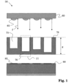
- Fig. 1 is a schematic illustration of an aspect of the invention, in a cross-sectional view. It shows, in an exploded view, three members, namely an optics member 60, a spacer member 70 and a detection member 80, which form together a device 50, more particularly an opto-electronic module 50.
- Optics member 60 comprises several passive optical components 65, in particular lenses 65.
- Passive optical components 65 have assigned nominal focal lengths, in particular all have the same nominal focal length. But - usually for manufacturing reasons - the focal lengths of the passive optical components 65 (more particularly: front focal lengths) deviate from their respective nominal focal length, as shown in Fig. 1 by the arrows referenced f.
- Detection member 80 can in particular be a semiconductor chip comprising active optical components 85 such as image sensors 85.
- Spacer member 70 contributes to ensuring a pre-defined distance cf. reference “g" in Fig. 1 ) between member 60 and member 80. But, moreover, it also contributes to an at least partial correction of the above-described deviations from the nominal focal lengths.
- Spacer member 70 comprises several light channels 77, one per each passive optical component 65. Each of the light channels 77 comprises a blind hole 75 and a portion of transparent material 76.
- the index of refraction of the material of spacer member 70 is different from (usually greater than) the index of refraction of vacuum or air which is usually present in the blind holes 75.
- the geometrical length g is (at least nominally) identical for each of the light channels 77; it corresponds to a (maximum or overall) vertical extension of spacer member 70.
- the lengths of the blind holes are different for differently deviating passive optical components 65.
- each active optical component 85 of member 80 e.g., detecting elements 85 such as image sensors 85
- each active optical component 85 records one sub-image, e.g., one plenoptic camera sub-image or one array camera sub-image, or one sub-image for one color or wavelength range, wherein in that case not all active optical components 85 record sub-images for the same color or wavelength range.
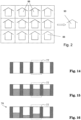
- the sub-images taken by the different active optical components 85 can be processed so as to derive from them a full (final) image.
- Fig. 2 illustrates that from a number of such sub-images 88, a full image 90 can be obtained.
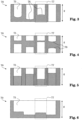
- a light channel may comprise a through-hole (cf. the right-most channel in Fig. 3 ).
- Fig. 4 it is also illustrated that material can be removed from both sides of the spacer member 70, i.e. from the object side (generally in all the Figures showing a spacer member meant to be towards the top of the drawing page, like in Fig. 1 ) at which an optics member will usually be located, and at the detector side (generally in all the Figures showing a spacer member meant to be towards the bottow of the drawing page, like in Fig. 1 ), at which an detection member will usually be located.
- spacer members illustrated in one of the Figures of the present patent application may be used as a spacer member in devices like the one illustrated in Fig. 1 , replacing the spacer member shown there.
- the light channels 77 may be separate from each other, in particular optically separate from each other.
- a portion of the spacer member may be made of a non-transparent material, in particular such that each light channel 77 is at least partially sourrounded by non-transparent material.
- Fig. 5 illustrates a spacer member 70 with non-transparently surrounded light channels 77, in a cross-sectional view, according to a non claimed example.
- each light channel 77 is made of a non-transparent material, e.g, of a hardened hardenable material such as a curable epoxy resin, whereas the inner portion is filled with a transparent material such as, again, a hardened hardenable material such as a curable epoxy resin, wherein said filling fills the respective light channel (i.e. in the illustrated case, the respective through-hole in spacer member 70) laterally completely, but (generally for at least one of the light channels) vertically only in part.
- a lateral cross-section through a light channel can be, e.g., circular or rectangular (with sharp or with rounded corners).
- Fig. 6 illustrates a spacer member 70 with not-separated light channels, in a cross-sectional view.
- a possible advantage of not-separated light channels is that a corresponding device can be (laterally) smaller, passive optical components (cf. Fig. 1 ) can be closer to each other, and detection members (cf. Fig. 1 ) can be closer to each other.
- Fig. 7 illustrates another spacer member 70, in a cross-sectional view. This is to illustrate that one can also fill liquid material into a blind-hole. Also this filled-in material may be hardened. The amount of filled-in material can be selected such that a sought compensation of manufacturing irregularities is achieved.
- Fig. 8 illustrates another spacer member 70, in a cross-sectional view. This is to illustrate that one can prepare, e.g., by means of replication, a wafer (or member) already implementing a compensation for manufacturing irregularities of an optics member. And furthermore, it illustrates that it is possible, in addition, to then fill liquid material into the blind-holes for fine-tuning the compensation.
- Fig. 9 illustrates another spacer member 70, in a cross-sectional view. This is to illustrate on the one hand that it is possible to carry out corrections / adjustments that (simultaneously) apply to all channels of a spacer member 70, and on the other hand that the detector side of a spacer member 70 does not necessarily have to describe a single plane (cf. also Fig. 4 ). But, it can be advantageous to provide that the detector side of a spacer member 70 describes a single plane (as is illustrated in most Figures of the present patent application), because in that case, the spacer member can be readily bonded to a detection member (cf. Fig. 1 ) without providing additional interfaces (between air and a higher refractive index material such as material of the spacer member or of the detection member), which again can result in less reflection losses and in a higher imaging quality.
- the general function of a device 50 (cf. Fig. 1 ) is that light impinging from an object side (above member 60 in Fig. 1 ) is imaged by passive optical components 65 through light channels 77 onto the active optical components 85 of member 80.
- Devices 50 can be used, e.g., in a communication device and/or in a camera such as in an array camera.
- the focal length of each of the passive optical components 65 is determined, and, in dependence of the result thereof, the blind holes are created (e.g., by drilling and/or laser ablation) having the appropriate length (cf., e.g., Figs. 1 , 3, 4, 6 , 9 , which can be interpreted accordingly); or a suitable spacer wafer is produced using replication already taking into account - by using a suitable replication master - the manufacturing irregularities to be compensated for (cf., e.g., Figs. 1 , 3 , 6 , 9 , which can be interpreted accordingly).
- these two approaches are combined by using a suitable spacer wafer already compensating to some extent for the manufacturing irregularities, by having blind holes of corresponding lengths, and then to apply further corrections, such as by changing the optical path length through light channels by means of which a sufficient compensation of the respective manufacturing irregularities has not yet been achieved (cf., e.g., Figs. 3, 4 , 8, 9 , which can be interpreted accordingly).
- further corrections are accomplished, by drilling and/or machining and/or cutting and/or laser ablation.
- Figs. 10 to 12 illustrate further possible aspects and non claimed embodiments.
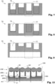
- Figs. 10 to 12 illustrate, in a cross-sectional view, a wafer stack 100 comprising an optics wafer OW comprising passive optical components 65 at least a portion of which have manufacturing irregularities such as focal lengths deviating from a nominal value, and, attached thereto, a spacer wafer stack 200.
- Optics wafer OW comprises a multitude of optics members 60
- spacer wafer stack 200 comprises a multitude of spacer members, wherein in wafer stack 100, each optics member is associated and aligned with a different one of the spacer members. Detection members and a detection wafer are not illustrated in Figs. 10 to 12 .
- Spacer wafer stack 200 comprises a spacer wafer SW1 and a spacer wafer SW2.
- Spacer wafer SW1 is made of a non-transparent material and can thus strongly contribute to optically mutally isolating light channels 77.
- Spacer wafer SW1 can furthermore be provided for ensuring a desired (vertical) distance between optics wafer OW and spacer wafer SW2.
- One particularity of wafer stack 200 is that spacer wafer SW2 comprises two layers ml, m2 of different (but transparent) materials. E.g., layer ml is made of glass, and layer m2 is made of a polymer material, or layer ml is made of a polymer material, and layer m2 is made of glass.
- the layer (ml) facing optics wafer OW is provided for providing mechanical stability, whereas the other layer (m2) (more particular, the material of which it is made) is mechanically less stable than (the material of) layer ml. And/or, it can be provided that, considering a method or process for removing material from spacer wafer SW2, the material of layer m2 is easier to remove than the material of layer ml. It is to be noted, however, that layer ml can, in general, also be dispensed with.
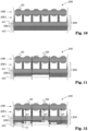
- Figs. 10 to 12 and more specifically, Figs. 11 and 12 , illustrate that it is possible to carry out a removal of material from a spacer wafer or from a spacer wafer stack 200 (or, more specifically from a layer m2) in two (or generally: two or more) processing steps. Removing material can allow to change the optical path length in light channels 77.
- Fig. 11 illustrates the wafer stack resulting from applying a first processing step to spacer wafer stack 200 of Fig. 10
- Fig. 12 illustrates the wafer stack 100 resulting from applying a second processing step to spacer wafer stack 200 of Fig. 11 .
- the two successively applied processing steps can be different processing steps, e.g., if both processing steps are carried out by means of milling, in the first processing step, a different milling tool may be used and possibly also a faster feed rate than in the second processing step may be applied. And it is also possible to combine different processing techniques in the processing steps, e.g., laser ablation first, and milling thereafter, or vice versa.
- the second processing step may in particular be a fine-tuning step (for optimizing the compensation effect).
- FIGs. 11 and 12 may be looked upon as illustrating a possible way of proceeding in case of multi-channel devices, such as four-channel devices with a 2 x 2 array of channels (cf. Figs. 11 and 12 ).
- multi-channel devices such as four-channel devices with a 2 x 2 array of channels (cf. Figs. 11 and 12 ).
- spacer members will usually be obtained which have different heights (vertical extensions) and thus different geometrical lengths gl, g2, g3 of their light channels, which, however, are equal for all light channels of one spacer member, but corrections for, e.g., focal lengths, can be made (in the second procesing step) individually for each channel.
- bonding of detection members to the spacer members will usually have to take place after separation of spacer wafer 200 which may be accomplished during separating wafer stack 100.
- Fig. 13 illustrates a two-times processed spacer member comprising more than one unitary parts (SW1, ml, m2), in a cross-sectional view, according to a non claimed example.
- spacer wafer SW2 is horizontally (laterally) mirrored, and, in addition, the (laterally defined) area in which material is removed in the second processing step is reduced with respect to what is illustrated in Fig. 12 .
- layer m2 of spacer wafer SW2 would be subjected to a first processing step (similar to what is illustrated in Fig. 11 ). This first processing step would in particular be applied simultaneously to all light channels of a spacer member (and typically using one and the same tool), but separately for different spacer members.
- spacer wafers SW1 and SW2 and optics wafer OW are bonded together so as to form a wafer stack 100. This may be accomplished in one or more steps. It is also possible that a detection wafer comprising a multitude of detection members (cf. Fig. 1 ) is bonded to spacer wafer SW2 already at this point - or this is accomplished thereafter.
- a so-obtained device can be, e.g., a computational camera or a module for a computational camera, or an array camera or a module for an array camera.
- Figs. 14 to 16 illustrate, in a cross-sectional view, a spacer member with non-transparently (laterally) encompassed light channels 77, according to a non claimed example.
- the example of Fig. 5 is similar thereto and, in fact, Figs. 14 to 16 allow to illustrate ways of obtaining a spacer wafer as illustrated in Fig. 5 .
- Fig. 14 illustrates a member of non-transparent material comprising through-holes as light channels, in a cross-sectional view
- Fig. 15 illustrates, in a cross-sectional view, the member of Fig. 14 , but with transparent material filled in the light channels
- Fig. 16 illustrates the member of Fig. 14 , with dfferent amounts of transparent material filled in the light channels, in a cross-sectional view.
- a wafer comprising a multitude of through-holes may be provided.
- Such a wafer can be obtained, e.g., as a unitary part, e.g., using a replication process.
- a liquid hardenable material is filled into the through holes and is thereafter hardened, e.g., cured.
- said wafer can be placed on a substrate such as on a mat of a silicone in order to avoid liquid material flowing out of the through-holes.
- the filled-in material is transparent.
- a polishing step may be applied to the so-obtained wafer, in order to have a high-quality optical surface at the detector side.
- the amount of liquid material filled in the holes is selected individually for each light channel, so as to accomplish the desired adjustment of optical path lengths.
- the amount of material filled in is (at least nominally) equal for all through-holes (i.e. for all light channels) of a spacer member, wherein it can be (at least nominally) equal for all through-holes (i.e. for all light channels) of a spacer wafer (cf- Fig. 15 ).
- a processing step is carried out, for adding more of a (or of the same) liquid hardenable material individually for the light channels and/or for removing a portion of said liquid hardenable material individually for the light channels.
- a fine-tuning step can also be applied in case of the before-addressed first way.
- a dispenser like known from electronics manufacturing for underfilling flip chips and the like
- machining or milling or drilling or laser ablation may be used.
- the invention may allow to mass produce high-precision optical devices on wafer scale at a very high yield.
- replication is used during (or for) manufacturing optics wafers and/or optics members and/or passive optical components, in particular when a replication step is used for manufacturing simultaneously (or in a single process) a multitude of optics members and/or of passive optical components, repeatable manufacturing irrgularities may occur which can very well be compensated for by means of the invention.
- replication may or may not be applied for accomplishing said compensation, e.g., for producing a compensating spacer wafer or compensating spacer members.
Landscapes
- Physics & Mathematics (AREA)
- Engineering & Computer Science (AREA)
- Optics & Photonics (AREA)
- General Physics & Mathematics (AREA)
- Plasma & Fusion (AREA)
- Mechanical Engineering (AREA)
- Spectroscopy & Molecular Physics (AREA)
- Lens Barrels (AREA)
- Solid State Image Pick-Up Elements (AREA)
- Camera Bodies And Camera Details Or Accessories (AREA)
- Studio Devices (AREA)
- Optical Couplings Of Light Guides (AREA)
- Optical Elements Other Than Lenses (AREA)
- Shaping Of Tube Ends By Bending Or Straightening (AREA)
- Casting Or Compression Moulding Of Plastics Or The Like (AREA)
Description
- The invention relates to the field of optics, more particularly micro-optics. In particular, it relates to wafer-level fabrication of optical devices such as optical systems, opto-electronic modules and cameras.
- From the international patent application published as
WO 2011/156928 A2 (filed on June 10, 2011 ), cameras and optical modules for cameras are known, which can be fabricated on wafer level. Therein, cameras and optical modules for cameras as well as methods for manufacturing the same are disclosed in some detail. - From
US 2004/165823 a method for manufacturing an optical device, according to the preamble ofclaim 1, is known. - "Active optical component": A light sensing or a light emitting component. E.g., a photodiode, an image sensor, an LED, an OLED, a laser chip.
- "Passive optical component": An optical component redirecting light by refraction and/or diffraction and/or reflection such as a lens, a prism, a mirror, or an optical system, wherein an optical system is a collection of such optical components possibly also comprising mechanical elements such as aperture stops, image screens, holders.
- "Opto-electronic module": A component in which at least one active and at least one passive optical component is comprised.
- "Replication": A technique by means of which a given structure or a negative thereof is reproduced. E.g., etching, embossing, imprinting, casting, molding.
- "Wafer": A substantially disk- or plate-like shaped item, its extension in one direction (z-direction or vertical direction) is small with respect to its extension in the other two directions (x- and y-directions or lateral directions). Usually, on a (non-blank) wafer, a plurality of like structures or items are arranged or provided therein, typically on a rectangular grid. A wafer may have opening or holes, and a wafer may even be free of material in a predominant portion of its lateral area. Although in many contexts, a wafer is understood to be prevailingly made of a semiconductor material, in the present patent application, this is explicitely not a limitation. Accordingly, a wafer may prevailingly be made of, e.g., a semiconductor material, a polymer material, a composite material comprising metals and polymers or polymers and glass materials. In particular, hardenable materials such as thermally or UV-curable polymers are interesting wafer materials in conjunction with the presented invention.
- "Lateral": cf. "Wafer"
- "Vertical": cf. "Wafer"
- "Light": Most generally electromagnetic radiation; more particularly electromagnetic radiation of the infrared, visible or ultraviolet portion of the electromagnetic spectrum.
- The invention is defined in
claim 1. Embodiments of the invention are set out in the dependent claims. - Below, the invention is described in more detail by means of examples and the included drawings. The figures show in a strongly schematized manner:
- Fig. 1
- an exploded view of a device, in a cross-sectional view;
- Fig. 2
- an illustration that from a number of sub-images, a full image can be obtained;
- Fig. 3
- a spacer member with lens shapes, in a cross-sectional view;
- Fig. 4
- a spacer member with lens shapes, in a cross-sectional view;
- Fig. 5
- a spacer member with non-transparently surrounded light channels, in a cross-sectional view;
- Fig. 6
- a spacer member with not-separated light channels, in a cross-sectional view;
- Fig. 7
- a spacer member, in a cross-sectional view;
- Fig. 8
- a spacer member, in a cross-sectional view;
- Fig. 9
- a spacer member, in a cross-sectional view;
- Fig. 10
- a detail of a wafer stack comprising spacer members comprising more than one unitary parts, in a cross-sectional view;
- Fig. 11
- a detail of the wafer stack of
Fig. 10 after a first processing step, in a cross-sectional view; - Fig. 12
- a detail of the wafer stack of
Figs. 10 and 11 after a second processing step, in a cross-sectional view; - Fig. 13
- a detail of a wafer stack comprising a two-times processed spacer member comprising more than one unitary parts, in a cross-sectional view;
- Fig. 14
- a member of non-transparent material comprising through-holes as light channels, in a cross-sectional view;
- Fig. 15
- the member of
Fig. 14 , with transparent material filled in the light channels, in a cross-sectional view; - Fig. 16
- the member of
Fig. 14 , with dfferent amounts of transparent material filled in the light channels, in a cross-sectional view. - The described embodiments are meant as examples.
-
Fig. 1 is a schematic illustration of an aspect of the invention, in a cross-sectional view. It shows, in an exploded view, three members, namely anoptics member 60, aspacer member 70 and adetection member 80, which form together adevice 50, more particularly an opto-electronic module 50. -
Optics member 60 comprises several passiveoptical components 65, inparticular lenses 65. Passiveoptical components 65 have assigned nominal focal lengths, in particular all have the same nominal focal length. But - usually for manufacturing reasons - the focal lengths of the passive optical components 65 (more particularly: front focal lengths) deviate from their respective nominal focal length, as shown inFig. 1 by the arrows referenced f. -
Detection member 80 can in particular be a semiconductor chip comprising activeoptical components 85 such asimage sensors 85. -
Spacer member 70 contributes to ensuring a pre-defined distance cf. reference "g" inFig. 1 ) betweenmember 60 andmember 80. But, moreover, it also contributes to an at least partial correction of the above-described deviations from the nominal focal lengths.Spacer member 70 comprises severallight channels 77, one per each passiveoptical component 65. Each of thelight channels 77 comprises ablind hole 75 and a portion oftransparent material 76. - The index of refraction of the material of
spacer member 70 is different from (usually greater than) the index of refraction of vacuum or air which is usually present in theblind holes 75. Thus, by adjusting the lengths of theblind holes 75 in dependence of the deviations of the focal length of the associated passiveoptical component 65 from the respective nominal focal lengths, deviations can be compensated, at least to some degree. The geometrical length g is (at least nominally) identical for each of thelight channels 77; it corresponds to a (maximum or overall) vertical extension ofspacer member 70. - Therefore, the lengths of the blind holes are different for differently deviating passive
optical components 65. - This way, it can be achieved that an imaging taking place using the different passive
optical components 65 with their different focal lengths results in the (nominally) desired imaging. And thus, each activeoptical component 85 ofmember 80, e.g., detectingelements 85 such asimage sensors 85, can record the desired image; without the individually chosen or adjusted blind holes, the recorded images would deviate or differ from the desired images, usually to an extent depending on the amount of manufacturing irregularities of the respective passiveoptical components 65. In particular, each activeoptical component 85 records one sub-image, e.g., one plenoptic camera sub-image or one array camera sub-image, or one sub-image for one color or wavelength range, wherein in that case not all activeoptical components 85 record sub-images for the same color or wavelength range. - The sub-images taken by the different active
optical components 85 can be processed so as to derive from them a full (final) image. -
Fig. 2 illustrates that from a number ofsuch sub-images 88, afull image 90 can be obtained. - There are also other possibilities to achieve a variation in optical path length between the
different light channels 77 despite of them having the same geometrical path length g, see, e.g., the patent claims. E.g., shapes such as lens-shapes can be produced in the optical paths, e.g., in the blind holes.Figs. 3 and 4 show, in a cross-sectional view, aspacer member 70 with blind holes having a curved (lens-shaped) bottom 78. In other words, lens elements are formed in the light channels. InFig. 3 , it is also illustrated that, according to a non claimed example but useful for understanding the invention, a light channel may comprise a through-hole (cf. the right-most channel inFig. 3 ). InFig. 4 , it is also illustrated that material can be removed from both sides of thespacer member 70, i.e. from the object side (generally in all the Figures showing a spacer member meant to be towards the top of the drawing page, like inFig. 1 ) at which an optics member will usually be located, and at the detector side (generally in all the Figures showing a spacer member meant to be towards the bottow of the drawing page, like inFig. 1 ), at which an detection member will usually be located. Generally, spacer members illustrated in one of the Figures of the present patent application may be used as a spacer member in devices like the one illustrated inFig. 1 , replacing the spacer member shown there. - The
light channels 77 may be separate from each other, in particular optically separate from each other. E.g., a portion of the spacer member may be made of a non-transparent material, in particular such that eachlight channel 77 is at least partially sourrounded by non-transparent material.Fig. 5 illustrates aspacer member 70 with non-transparently surroundedlight channels 77, in a cross-sectional view, according to a non claimed example. The outer portion of eachlight channel 77 is made of a non-transparent material, e.g, of a hardened hardenable material such as a curable epoxy resin, whereas the inner portion is filled with a transparent material such as, again, a hardened hardenable material such as a curable epoxy resin, wherein said filling fills the respective light channel (i.e. in the illustrated case, the respective through-hole in spacer member 70) laterally completely, but (generally for at least one of the light channels) vertically only in part. A lateral cross-section through a light channel can be, e.g., circular or rectangular (with sharp or with rounded corners). - But it is also possible to provide that at least one of the
light channels 77 is adjacent to at least one other light channels of the spacer member or is even partially overlapping with at least one other light channels of the spacer member.Fig. 6 illustrates aspacer member 70 with not-separated light channels, in a cross-sectional view. - A possible advantage of optically separated light channels, cf., e.g.,
Fig. 5 , is the possibility to suppress cross-talk between the light channels. A possible advantage of not-separated light channels is that a corresponding device can be (laterally) smaller, passive optical components (cf.Fig. 1 ) can be closer to each other, and detection members (cf.Fig. 1 ) can be closer to each other. -
Fig. 7 illustrates anotherspacer member 70, in a cross-sectional view. This is to illustrate that one can also fill liquid material into a blind-hole. Also this filled-in material may be hardened. The amount of filled-in material can be selected such that a sought compensation of manufacturing irregularities is achieved. -
Fig. 8 illustrates anotherspacer member 70, in a cross-sectional view. This is to illustrate that one can prepare, e.g., by means of replication, a wafer (or member) already implementing a compensation for manufacturing irregularities of an optics member. And furthermore, it illustrates that it is possible, in addition, to then fill liquid material into the blind-holes for fine-tuning the compensation. -
Fig. 9 illustrates anotherspacer member 70, in a cross-sectional view. This is to illustrate on the one hand that it is possible to carry out corrections / adjustments that (simultaneously) apply to all channels of aspacer member 70, and on the other hand that the detector side of aspacer member 70 does not necessarily have to describe a single plane (cf. alsoFig. 4 ). But, it can be advantageous to provide that the detector side of aspacer member 70 describes a single plane (as is illustrated in most Figures of the present patent application), because in that case, the spacer member can be readily bonded to a detection member (cf.Fig. 1 ) without providing additional interfaces (between air and a higher refractive index material such as material of the spacer member or of the detection member), which again can result in less reflection losses and in a higher imaging quality. - The general function of a device 50 (cf.
Fig. 1 ) is that light impinging from an object side (abovemember 60 inFig. 1 ) is imaged by passiveoptical components 65 throughlight channels 77 onto the activeoptical components 85 ofmember 80. -
Devices 50 can be used, e.g., in a communication device and/or in a camera such as in an array camera. - It is suggested to manufacture any of, in particular all of the
members device 50 very efficient, including simplifying accomplishing the individual adjustments suggested for the compensating for of the manufacturing irregularities. - E.g., the focal length of each of the passive
optical components 65 is determined, and, in dependence of the result thereof, the blind holes are created (e.g., by drilling and/or laser ablation) having the appropriate length (cf., e.g.,Figs. 1 ,3, 4, 6 ,9 , which can be interpreted accordingly); or a suitable spacer wafer is produced using replication already taking into account - by using a suitable replication master - the manufacturing irregularities to be compensated for (cf., e.g.,Figs. 1 ,3 ,6 ,9 , which can be interpreted accordingly). - According to the invention, these two approaches are combined by using a suitable spacer wafer already compensating to some extent for the manufacturing irregularities, by having blind holes of corresponding lengths, and then to apply further corrections, such as by changing the optical path length through light channels by means of which a sufficient compensation of the respective manufacturing irregularities has not yet been achieved (cf., e.g.,
Figs. 3, 4 ,8, 9 , which can be interpreted accordingly). These further corrections are accomplished, by drilling and/or machining and/or cutting and/or laser ablation. -
Figs. 10 to 12 illustrate further possible aspects and non claimed embodiments. -
Figs. 10 to 12 illustrate, in a cross-sectional view, awafer stack 100 comprising an optics wafer OW comprising passiveoptical components 65 at least a portion of which have manufacturing irregularities such as focal lengths deviating from a nominal value, and, attached thereto, aspacer wafer stack 200. Optics wafer OW comprises a multitude ofoptics members 60, andspacer wafer stack 200 comprises a multitude of spacer members, wherein inwafer stack 100, each optics member is associated and aligned with a different one of the spacer members. Detection members and a detection wafer are not illustrated inFigs. 10 to 12 . -
Spacer wafer stack 200 comprises a spacer wafer SW1 and a spacer wafer SW2. Spacer wafer SW1 is made of a non-transparent material and can thus strongly contribute to optically mutally isolatinglight channels 77. Spacer wafer SW1 can furthermore be provided for ensuring a desired (vertical) distance between optics wafer OW and spacer wafer SW2. One particularity ofwafer stack 200 is that spacer wafer SW2 comprises two layers ml, m2 of different (but transparent) materials. E.g., layer ml is made of glass, and layer m2 is made of a polymer material, or layer ml is made of a polymer material, and layer m2 is made of glass. It can, more generally, be provided that the layer (ml) facing optics wafer OW is provided for providing mechanical stability, whereas the other layer (m2) (more particular, the material of which it is made) is mechanically less stable than (the material of) layer ml. And/or, it can be provided that, considering a method or process for removing material from spacer wafer SW2, the material of layer m2 is easier to remove than the material of layer ml. It is to be noted, however, that layer ml can, in general, also be dispensed with. - It is furthermore generally possible to consider layers ml and m2, respectively, as distinct spacer wafers which, however, are bonded to each other.
- More specifically, as illustrated in
Figs. 11 and 12 , it is possible to provide that a removal of material for compensating for manufacturing irregularities of optics wafer OW takes place in layer m2 only. - Furthermore,
Figs. 10 to 12 , and more specifically,Figs. 11 and 12 , illustrate that it is possible to carry out a removal of material from a spacer wafer or from a spacer wafer stack 200 (or, more specifically from a layer m2) in two (or generally: two or more) processing steps. Removing material can allow to change the optical path length inlight channels 77. In this case,Fig. 11 illustrates the wafer stack resulting from applying a first processing step tospacer wafer stack 200 ofFig. 10, and Fig. 12 illustrates thewafer stack 100 resulting from applying a second processing step tospacer wafer stack 200 ofFig. 11 . The two successively applied processing steps can be different processing steps, e.g., if both processing steps are carried out by means of milling, in the first processing step, a different milling tool may be used and possibly also a faster feed rate than in the second processing step may be applied. And it is also possible to combine different processing techniques in the processing steps, e.g., laser ablation first, and milling thereafter, or vice versa. - The second processing step may in particular be a fine-tuning step (for optimizing the compensation effect).
- And even further,
Figs. 11 and 12 may be looked upon as illustrating a possible way of proceeding in case of multi-channel devices, such as four-channel devices with a 2 x 2 array of channels (cf.Figs. 11 and 12 ). As illustrated inFig. 11 , it is possible to carry out the first processing step individually for one device, i.e. for one spacer member, but carry out the second processing step individually for each light channel 77 (cf.Fig. 12 ). - Thus, after a separation step (cf. the thick dashed lines in
Fig. 12 ), spacer members will usually be obtained which have different heights (vertical extensions) and thus different geometrical lengths gl, g2, g3 of their light channels, which, however, are equal for all light channels of one spacer member, but corrections for, e.g., focal lengths, can be made (in the second procesing step) individually for each channel. - In an embodiment like the one of
Figs. 10 to 12 , bonding of detection members to the spacer members will usually have to take place after separation ofspacer wafer 200 which may be accomplished during separatingwafer stack 100. -
Fig. 13 illustrates a two-times processed spacer member comprising more than one unitary parts (SW1, ml, m2), in a cross-sectional view, according to a non claimed example. In fact,Fig. 13 very much corresponds toFig. 12 , but spacer wafer SW2 is horizontally (laterally) mirrored, and, in addition, the (laterally defined) area in which material is removed in the second processing step is reduced with respect to what is illustrated inFig. 12 . - In case of the example like illustrated in
Fig. 13 , data would be obtained on manufacturing irregularities of passiveoptical components 65, or, in particular, of sets of passive optical components composed of the passive optical components belonging to one and the same light channel. Based on such data, layer m2 of spacer wafer SW2 would be subjected to a first processing step (similar to what is illustrated inFig. 11 ). This first processing step would in particular be applied simultaneously to all light channels of a spacer member (and typically using one and the same tool), but separately for different spacer members. - Thereafter, possibly based on further data on manufacturing irregularities of passive optical components 65 (possibly obtained from a preliminary assembly of optics wafer OW, spacer wafer SW1 and spacer wafer SW2), a second processing step is applied, in which each light channel is individually addressed.
- Then, spacer wafers SW1 and SW2 and optics wafer OW are bonded together so as to form a
wafer stack 100. This may be accomplished in one or more steps. It is also possible that a detection wafer comprising a multitude of detection members (cf.Fig. 1 ) is bonded to spacer wafer SW2 already at this point - or this is accomplished thereafter. - Finally, a separation step is applied in which separate devices are obtained, e.g., by dicing or laser cutting. A so-obtained device can be, e.g., a computational camera or a module for a computational camera, or an array camera or a module for an array camera.
-
Figs. 14 to 16 illustrate, in a cross-sectional view, a spacer member with non-transparently (laterally) encompassedlight channels 77, according to a non claimed example. The example ofFig. 5 is similar thereto and, in fact,Figs. 14 to 16 allow to illustrate ways of obtaining a spacer wafer as illustrated inFig. 5 . -
Fig. 14 illustrates a member of non-transparent material comprising through-holes as light channels, in a cross-sectional view;Fig. 15 illustrates, in a cross-sectional view, the member ofFig. 14 , but with transparent material filled in the light channels; andFig. 16 illustrates the member ofFig. 14 , with dfferent amounts of transparent material filled in the light channels, in a cross-sectional view. - For obtaining a
spacer member 70 like illustrated inFigs. 5 and16 , a wafer comprising a multitude of through-holes (cf.Fig. 14 ) may be provided. Such a wafer can be obtained, e.g., as a unitary part, e.g., using a replication process. Then, a liquid hardenable material is filled into the through holes and is thereafter hardened, e.g., cured. During this, said wafer can be placed on a substrate such as on a mat of a silicone in order to avoid liquid material flowing out of the through-holes. After hardening, the filled-in material is transparent. Possibly, a polishing step may be applied to the so-obtained wafer, in order to have a high-quality optical surface at the detector side. - In a first way of obtaining a
spacer member 70 like illustrated inFigs. 5 and16 , the amount of liquid material filled in the holes is selected individually for each light channel, so as to accomplish the desired adjustment of optical path lengths. In a second way, the amount of material filled in is (at least nominally) equal for all through-holes (i.e. for all light channels) of a spacer member, wherein it can be (at least nominally) equal for all through-holes (i.e. for all light channels) of a spacer wafer (cf-Fig. 15 ). - After hardening, then, a processing step is carried out, for adding more of a (or of the same) liquid hardenable material individually for the light channels and/or for removing a portion of said liquid hardenable material individually for the light channels. Such a fine-tuning step, however, can also be applied in case of the before-addressed first way.
- For filling-in liquid material, e.g., a dispenser (like known from electronics manufacturing for underfilling flip chips and the like) may be used. For removing material, machining or milling or drilling or laser ablation may be used.
- As will have become clear from the above, the invention may allow to mass produce high-precision optical devices on wafer scale at a very high yield. In particular if replication is used during (or for) manufacturing optics wafers and/or optics members and/or passive optical components, in particular when a replication step is used for manufacturing simultaneously (or in a single process) a multitude of optics members and/or of passive optical components, repeatable manufacturing irrgularities may occur which can very well be compensated for by means of the invention. Therein, replication may or may not be applied for accomplishing said compensation, e.g., for producing a compensating spacer wafer or compensating spacer members.
Claims (6)
- A method for manufacturing a device (50), said method comprising the steps of-- providing a spacer wafer comprising M ≥ 2 spacer members (70), wherein M is an integer, each of said M spacer members (70) comprising N ≥ 2 light channels (77), N being an integer, and wherein a plurality of said M x N light channels (77) each comprise a blind hole (75) forming a portion of the respective light channel;-- providing an optics wafer (OW) comprising M optics members (60), each of said M optics members (60) comprising N sets of passive optical components (65) comprising one or more passive optical components each;-- providing a detection wafer comprising M detection members (80), each of said M detection members (80) comprising N active optical components (85);-- forming a wafer stack (100) comprising said optics wafer (OW), said detection wafer and, arranged between said optics wafer (OW) and said detection wafer, said spacer wafer (SW2);wherein each of said M spacer members (70) is associated with a different one of said optics members (60) and associated with a different one of said detection members (80), andwherein for each of said M spacer members (70), each of the respective N light channels (77) is associated with a different one of the N sets of passive optical components (65) of the associated optics member (60) and associated with a different one of the N active optical components (85) of the associated detection members (80), andwherein, for at least a first spacer member of said M spacer members (70) and the associated optics members (60) and the associated detection members (80),-- all of the N light channels (77) of the first spacer member provide an identical geometrical path length for light travelling from the associated set of passive optical components (65) of the associated optics member (60) through the respective light channel (77) to the associated active optical component of the associated detection member (80), and-- an optical path length for light travelling from a first of the N sets of passive optical components (65) of a respective optics member (60) through the associated light channel (77) of the first spacer member to the associated active optical component (85) is different from an optical path length for light travelling from a second of said N sets of passive optical components (65) through the respective associated light channel (77) of the first spacer member to the respective associated active optical component (85);wherein for each of said M x N light channels (77), said optical path length has a value related to and/or is chosen in dependence of manufacturing irregularities of the passive optical components of the set of passive optical components (65) of the respective associated optics member (60), and
wherein the method comprises manufacturing said spacer wafer (SW2) using a replication step, wherein a replication master used in said replication step is designed for accomplishing said different optical path lengths of the light channels (77),and wherein the spacer wafer (SW2) obtained by the replication step is subjected to a further processing step comprising increasing the precision of optical path lengths of light channels (77) of the spacer wafer (SW2) obtained by the further processing step,characterized in that,said further processing step comprises removing material from the spacer member, and wherein a length of one or more blind holes in said spacer wafer is increased by means of cutting and/or machining and/or drilling and/or laser ablating. - The method according to claim 1, comprising separating said wafer stack (100) into a multitude of modules, each comprising one of said spacer members (70), one of said optics members (60) and one of said detection members (80), in particular each comprising exactly one of said spacer members (70), exactly one of said optics members (60) and exactly one of said detection members (80).
- The method according to claim 1, comprising measuring said manufacturing irregularities.
- The method according to any preceding claim, wherein said spacer wafer (SW2) comprises a first layer (m1) and a second layer (m2) which are made of mutually different materials.
- The method according to claim 4, wherein the method comprises adjusting said optical path by removing material from said second layer (m2), and optionally wherein said second layer (m2) is made of a polymer material.
- The method according to any preceding claim, wherein said device is a camera or an opto-electronic module for a camera.
Applications Claiming Priority (2)
| Application Number | Priority Date | Filing Date | Title |
|---|---|---|---|
| US201161527355P | 2011-08-25 | 2011-08-25 | |
| PCT/CH2012/000200 WO2013026174A2 (en) | 2011-08-25 | 2012-08-24 | Wafer-level fabrication of optical devices. in particular of modules for computational cameras |
Publications (2)
| Publication Number | Publication Date |
|---|---|
| EP2748853A2 EP2748853A2 (en) | 2014-07-02 |
| EP2748853B1 true EP2748853B1 (en) | 2023-10-11 |
Family
ID=46969906
Family Applications (2)
| Application Number | Title | Priority Date | Filing Date |
|---|---|---|---|
| EP12768696.2A Active EP2748854B1 (en) | 2011-08-25 | 2012-08-24 | Wafer-level fabrication of optical devices with front focal length correction |
| EP12768695.4A Active EP2748853B1 (en) | 2011-08-25 | 2012-08-24 | Wafer-level fabrication of optical devices. in particular of modules for computational cameras |
Family Applications Before (1)
| Application Number | Title | Priority Date | Filing Date |
|---|---|---|---|
| EP12768696.2A Active EP2748854B1 (en) | 2011-08-25 | 2012-08-24 | Wafer-level fabrication of optical devices with front focal length correction |
Country Status (8)
| Country | Link |
|---|---|
| US (2) | US20140307081A1 (en) |
| EP (2) | EP2748854B1 (en) |
| JP (2) | JP6223975B2 (en) |
| KR (2) | KR102056501B1 (en) |
| CN (2) | CN103890948B (en) |
| SG (4) | SG2014008726A (en) |
| TW (3) | TWI567956B (en) |
| WO (2) | WO2013026174A2 (en) |
Families Citing this family (23)
| Publication number | Priority date | Publication date | Assignee | Title |
|---|---|---|---|---|
| US20130122247A1 (en) * | 2011-11-10 | 2013-05-16 | Omnivision Technologies, Inc. | Spacer Wafer For Wafer-Level Camera And Method For Manufacturing Same |
| US9595553B2 (en) | 2012-11-02 | 2017-03-14 | Heptagon Micro Optics Pte. Ltd. | Optical modules including focal length adjustment and fabrication of the optical modules |
| CN105765722B (en) | 2013-11-22 | 2019-10-22 | 赫普塔冈微光有限公司 | Compact Optoelectronic Module |
| US9977153B2 (en) | 2014-02-07 | 2018-05-22 | Heptagon Micro Optics Pte. Ltd. | Stacks of arrays of beam shaping elements including stacking, self-alignment and/or self-centering features |
| WO2015126328A1 (en) * | 2014-02-18 | 2015-08-27 | Heptagon Micro Optics Pte. Ltd. | Optical modules including customizable spacers for focal length adjustment and/or reduction of tilt, and fabrication of the optical modules |
| WO2015191001A1 (en) | 2014-06-10 | 2015-12-17 | Heptagon Micro Optics Pte. Ltd. | Optoelectronic modules including hybrid arrangements of beam shaping elements, and imaging devices incorporating the same |
| US9711552B2 (en) * | 2014-08-19 | 2017-07-18 | Heptagon Micro Optics Pte. Ltd. | Optoelectronic modules having a silicon substrate, and fabrication methods for such modules |
| US9507143B2 (en) | 2014-09-19 | 2016-11-29 | Intel Corporation | Compact illumination system |
| EP3207416B1 (en) | 2014-10-14 | 2020-02-26 | Heptagon Micro Optics Pte. Ltd. | Optical element stack assemblies |
| US20160307881A1 (en) * | 2015-04-20 | 2016-10-20 | Advanced Semiconductor Engineering, Inc. | Optical sensor module and method for manufacturing the same |
| KR102329129B1 (en) * | 2015-05-12 | 2021-11-19 | 삼성전자주식회사 | Image encoding method and apparatus for compensating for sample values, and image decoding method and apparatus for compensating for sample values |
| WO2016191142A2 (en) * | 2015-05-27 | 2016-12-01 | Verily Life Sciences Llc | Nanophotonic hyperspectral/lightfield superpixel imager |
| JP6619174B2 (en) * | 2015-07-31 | 2019-12-11 | ソニーセミコンダクタソリューションズ株式会社 | Manufacturing apparatus and method |
| WO2017023211A1 (en) * | 2015-08-06 | 2017-02-09 | Heptagon Micro Optics Pte. Ltd. | Optical modules including customizable spacers for focal length adjustment and/or reduction of tilt, and fabrication of the optical modules |
| DE102015215833A1 (en) | 2015-08-19 | 2017-02-23 | Fraunhofer-Gesellschaft zur Förderung der angewandten Forschung e.V. | Multi-aperture imaging device with optical substrate |
| CN108700721B (en) | 2015-11-12 | 2021-12-31 | 赫普塔冈微光有限公司 | Optical element stack assembly |
| KR20170073910A (en) | 2015-12-21 | 2017-06-29 | 에스케이하이닉스 주식회사 | Light field imaging device and method for fabricating the same |
| DE102016200285A1 (en) * | 2016-01-13 | 2017-07-13 | Fraunhofer-Gesellschaft zur Förderung der angewandten Forschung e.V. | Multi-aperture imaging apparatus, imaging system and method for detecting an object area |
| CN108941932A (en) * | 2017-05-23 | 2018-12-07 | 东莞东阳光科研发有限公司 | Artificial lens preparation method |
| US10677964B2 (en) * | 2017-10-23 | 2020-06-09 | Omnivision Technologies, Inc. | Lens wafer assembly and associated method for manufacturing a stepped spacer wafer |
| WO2020183600A1 (en) | 2019-03-12 | 2020-09-17 | オリンパス株式会社 | Endoscopic imaging device and endoscope |
| JP7654570B2 (en) | 2020-01-30 | 2025-04-01 | 古河電気工業株式会社 | Optical module and optical device |
| US11664399B2 (en) * | 2021-02-01 | 2023-05-30 | Visera Technologies Company Limited | Solid-state image sensor |
Citations (2)
| Publication number | Priority date | Publication date | Assignee | Title |
|---|---|---|---|---|
| US20040165823A1 (en) * | 2001-02-09 | 2004-08-26 | Morris James E. | Compensation and/or variation of wafer level produced lenses and resultant structures |
| US20060044450A1 (en) * | 2002-09-17 | 2006-03-02 | Koninklijke Philips Electronics, N.C. | Camera device, method of manufacturing a camera device, wafer scale package |
Family Cites Families (24)
| Publication number | Priority date | Publication date | Assignee | Title |
|---|---|---|---|---|
| US5232549A (en) * | 1992-04-14 | 1993-08-03 | Micron Technology, Inc. | Spacers for field emission display fabricated via self-aligned high energy ablation |
| DE10058305A1 (en) * | 2000-11-24 | 2002-06-06 | Wacker Siltronic Halbleitermat | Process for the surface polishing of silicon wafers |
| DE102005002545A1 (en) | 2005-01-19 | 2006-07-20 | Airbus Deutschland Gmbh | Power buffer device for e.g. lift drive of trolley-lift in aircraft, has power capacitor to store power in electric field, and power transfer device supplying power to load, and designed as power supply device for larger power output |
| CA2558898C (en) * | 2005-09-07 | 2013-11-05 | Purdue Research Foundation | Laser assisted machining process with distributed lasers |
| JP2007110588A (en) * | 2005-10-17 | 2007-04-26 | Funai Electric Co Ltd | Compound eye imaging device |
| CN101009779B (en) | 2006-01-24 | 2010-06-16 | 采钰科技股份有限公司 | Image sensing module for high-precision imaging control |
| US7721564B2 (en) | 2006-11-21 | 2010-05-25 | B/E Aerospace, Inc. | Wild frequency avionic refrigeration system and controller therefor |
| US7692256B2 (en) * | 2007-03-23 | 2010-04-06 | Heptagon Oy | Method of producing a wafer scale package |
| US7812869B2 (en) * | 2007-05-11 | 2010-10-12 | Aptina Imaging Corporation | Configurable pixel array system and method |
| KR101575915B1 (en) * | 2007-11-27 | 2015-12-08 | 헵타곤 마이크로 옵틱스 피티이. 리미티드 | Encapsulated lens stack |
| EP2223173B1 (en) | 2007-12-19 | 2013-09-04 | Heptagon Micro Optics Pte. Ltd. | Camera device and manufacturing methods therefor |
| US20090159200A1 (en) | 2007-12-19 | 2009-06-25 | Heptagon Oy | Spacer element and method for manufacturing a spacer element |
| TWI478808B (en) * | 2007-12-19 | 2015-04-01 | Heptagon Micro Optics Pte Ltd | Manufacturing optical elements |
| US8319301B2 (en) * | 2008-02-11 | 2012-11-27 | Omnivision Technologies, Inc. | Self-aligned filter for an image sensor |
| CN102037383B (en) * | 2008-03-27 | 2014-09-17 | 数字光学公司 | Optical device including at least one replicated surface and associated methods |
| WO2010074743A1 (en) * | 2008-12-22 | 2010-07-01 | Tessera North America, Inc. | Focus compensation for thin cameras |
| TW201115205A (en) | 2009-03-18 | 2011-05-01 | Artificial Muscle Inc | Wafer level optical system |
| JP2011018974A (en) * | 2009-07-07 | 2011-01-27 | Renesas Electronics Corp | D/a converter |
| US8193599B2 (en) * | 2009-09-02 | 2012-06-05 | Himax Semiconductor, Inc. | Fabricating method and structure of a wafer level module |
| US8059341B2 (en) * | 2009-09-23 | 2011-11-15 | Visera Technologies Company Limited | Lens assembly and method for forming the same |
| EP2491590B1 (en) | 2009-10-20 | 2015-08-05 | FLIR Systems Trading Belgium BVBA | Focus compensation for optical elements and applications thereof |
| US8885257B2 (en) * | 2009-10-20 | 2014-11-11 | Flir Systems Trading Belgium Bvba | Focus compensation for optical elements and applications thereof |
| WO2011063347A2 (en) | 2009-11-20 | 2011-05-26 | Pelican Imaging Corporation | Capturing and processing of images using monolithic camera array with heterogeneous imagers |
| WO2011156928A2 (en) | 2010-06-14 | 2011-12-22 | Heptagon Oy | Camera, and method of manufacturing a plurality of cameras |
-
2012
- 2012-08-24 SG SG2014008726A patent/SG2014008726A/en unknown
- 2012-08-24 US US14/239,334 patent/US20140307081A1/en not_active Abandoned
- 2012-08-24 EP EP12768696.2A patent/EP2748854B1/en active Active
- 2012-08-24 SG SG10201606884TA patent/SG10201606884TA/en unknown
- 2012-08-24 US US14/239,362 patent/US10444477B2/en active Active
- 2012-08-24 WO PCT/CH2012/000200 patent/WO2013026174A2/en not_active Ceased
- 2012-08-24 CN CN201280052514.0A patent/CN103890948B/en active Active
- 2012-08-24 WO PCT/CH2012/000201 patent/WO2013026175A1/en not_active Ceased
- 2012-08-24 CN CN201280052516.XA patent/CN103890949B/en active Active
- 2012-08-24 JP JP2014526351A patent/JP6223975B2/en active Active
- 2012-08-24 JP JP2014526352A patent/JP6282225B2/en active Active
- 2012-08-24 KR KR1020147007081A patent/KR102056501B1/en active Active
- 2012-08-24 SG SG10201606882XA patent/SG10201606882XA/en unknown
- 2012-08-24 KR KR1020147007074A patent/KR101966480B1/en not_active Expired - Fee Related
- 2012-08-24 EP EP12768695.4A patent/EP2748853B1/en active Active
- 2012-08-24 SG SG2014008718A patent/SG2014008718A/en unknown
- 2012-08-27 TW TW101131007A patent/TWI567956B/en not_active IP Right Cessation
- 2012-08-27 TW TW105134073A patent/TWI620310B/en not_active IP Right Cessation
- 2012-08-27 TW TW101131008A patent/TWI582969B/en active
Patent Citations (2)
| Publication number | Priority date | Publication date | Assignee | Title |
|---|---|---|---|---|
| US20040165823A1 (en) * | 2001-02-09 | 2004-08-26 | Morris James E. | Compensation and/or variation of wafer level produced lenses and resultant structures |
| US20060044450A1 (en) * | 2002-09-17 | 2006-03-02 | Koninklijke Philips Electronics, N.C. | Camera device, method of manufacturing a camera device, wafer scale package |
Also Published As
| Publication number | Publication date |
|---|---|
| CN103890949B (en) | 2017-10-03 |
| TW201316497A (en) | 2013-04-16 |
| TW201724487A (en) | 2017-07-01 |
| KR102056501B1 (en) | 2019-12-16 |
| TWI620310B (en) | 2018-04-01 |
| CN103890948A (en) | 2014-06-25 |
| JP6282225B2 (en) | 2018-02-21 |
| KR20140054280A (en) | 2014-05-08 |
| US20140299587A1 (en) | 2014-10-09 |
| WO2013026174A3 (en) | 2013-04-11 |
| JP6223975B2 (en) | 2017-11-01 |
| CN103890949A (en) | 2014-06-25 |
| EP2748854A1 (en) | 2014-07-02 |
| EP2748853A2 (en) | 2014-07-02 |
| TWI567956B (en) | 2017-01-21 |
| WO2013026174A2 (en) | 2013-02-28 |
| TWI582969B (en) | 2017-05-11 |
| KR101966480B1 (en) | 2019-04-05 |
| TW201327790A (en) | 2013-07-01 |
| SG2014008718A (en) | 2014-04-28 |
| US10444477B2 (en) | 2019-10-15 |
| WO2013026175A1 (en) | 2013-02-28 |
| CN103890948B (en) | 2017-12-01 |
| US20140307081A1 (en) | 2014-10-16 |
| JP2014524597A (en) | 2014-09-22 |
| SG10201606884TA (en) | 2016-10-28 |
| EP2748854B1 (en) | 2021-06-02 |
| JP2014526067A (en) | 2014-10-02 |
| SG2014008726A (en) | 2014-04-28 |
| SG10201606882XA (en) | 2016-10-28 |
| KR20140068984A (en) | 2014-06-09 |
Similar Documents
| Publication | Publication Date | Title |
|---|---|---|
| US20140307081A1 (en) | Wafer-level fabrication of optical devices, in particular of modules for computational cameras | |
| US10373996B2 (en) | Optical modules including focal length adjustment and fabrication of the optical modules | |
| CN101512767B (en) | Optoelectronic products and manufacturing method thereof | |
| KR101713135B1 (en) | Focus compensation for optical elements and applications thereof | |
| EP2943820B1 (en) | A lens array and a method of making a lens array | |
| US7964432B2 (en) | Method of manufacturing lenses, in particular for an integrated imager | |
| WO2015080575A1 (en) | A method for manufacturing an optical assembly |
Legal Events
| Date | Code | Title | Description |
|---|---|---|---|
| PUAI | Public reference made under article 153(3) epc to a published international application that has entered the european phase |
Free format text: ORIGINAL CODE: 0009012 |
|
| 17P | Request for examination filed |
Effective date: 20140204 |
|
| AK | Designated contracting states |
Kind code of ref document: A2 Designated state(s): AL AT BE BG CH CY CZ DE DK EE ES FI FR GB GR HR HU IE IS IT LI LT LU LV MC MK MT NL NO PL PT RO RS SE SI SK SM TR |
|
| DAX | Request for extension of the european patent (deleted) | ||
| 17Q | First examination report despatched |
Effective date: 20150731 |
|
| STAA | Information on the status of an ep patent application or granted ep patent |
Free format text: STATUS: EXAMINATION IS IN PROGRESS |
|
| RIC1 | Information provided on ipc code assigned before grant |
Ipc: B23K 26/361 20140101ALI20221007BHEP Ipc: H01L 27/146 20060101AFI20221007BHEP |
|
| GRAP | Despatch of communication of intention to grant a patent |
Free format text: ORIGINAL CODE: EPIDOSNIGR1 |
|
| STAA | Information on the status of an ep patent application or granted ep patent |
Free format text: STATUS: GRANT OF PATENT IS INTENDED |
|
| INTG | Intention to grant announced |
Effective date: 20221128 |
|
| GRAJ | Information related to disapproval of communication of intention to grant by the applicant or resumption of examination proceedings by the epo deleted |
Free format text: ORIGINAL CODE: EPIDOSDIGR1 |
|
| STAA | Information on the status of an ep patent application or granted ep patent |
Free format text: STATUS: EXAMINATION IS IN PROGRESS |
|
| INTC | Intention to grant announced (deleted) | ||
| GRAP | Despatch of communication of intention to grant a patent |
Free format text: ORIGINAL CODE: EPIDOSNIGR1 |
|
| STAA | Information on the status of an ep patent application or granted ep patent |
Free format text: STATUS: GRANT OF PATENT IS INTENDED |
|
| INTG | Intention to grant announced |
Effective date: 20230519 |
|
| RIN1 | Information on inventor provided before grant (corrected) |
Inventor name: HEIMGARTNER, STEPHAN Inventor name: ROENTGEN, PETER Inventor name: BIETSCH, ALEXANDER Inventor name: MALUCK, MATTHIAS Inventor name: RUDMANN, HARTMUT |
|
| P01 | Opt-out of the competence of the unified patent court (upc) registered |
Effective date: 20230613 |
|
| GRAS | Grant fee paid |
Free format text: ORIGINAL CODE: EPIDOSNIGR3 |
|
| GRAA | (expected) grant |
Free format text: ORIGINAL CODE: 0009210 |
|
| STAA | Information on the status of an ep patent application or granted ep patent |
Free format text: STATUS: THE PATENT HAS BEEN GRANTED |
|
| AK | Designated contracting states |
Kind code of ref document: B1 Designated state(s): AL AT BE BG CH CY CZ DE DK EE ES FI FR GB GR HR HU IE IS IT LI LT LU LV MC MK MT NL NO PL PT RO RS SE SI SK SM TR |
|
| REG | Reference to a national code |
Ref country code: GB Ref legal event code: FG4D |
|
| REG | Reference to a national code |
Ref country code: CH Ref legal event code: EP |
|
| REG | Reference to a national code |
Ref country code: DE Ref legal event code: R096 Ref document number: 602012080178 Country of ref document: DE |
|
| REG | Reference to a national code |
Ref country code: IE Ref legal event code: FG4D |
|
| REG | Reference to a national code |
Ref country code: LT Ref legal event code: MG9D |
|
| REG | Reference to a national code |
Ref country code: NL Ref legal event code: MP Effective date: 20231011 |
|
| REG | Reference to a national code |
Ref country code: AT Ref legal event code: MK05 Ref document number: 1621104 Country of ref document: AT Kind code of ref document: T Effective date: 20231011 |
|
| PG25 | Lapsed in a contracting state [announced via postgrant information from national office to epo] |
Ref country code: NL Free format text: LAPSE BECAUSE OF FAILURE TO SUBMIT A TRANSLATION OF THE DESCRIPTION OR TO PAY THE FEE WITHIN THE PRESCRIBED TIME-LIMIT Effective date: 20231011 |
|
| PG25 | Lapsed in a contracting state [announced via postgrant information from national office to epo] |
Ref country code: GR Free format text: LAPSE BECAUSE OF FAILURE TO SUBMIT A TRANSLATION OF THE DESCRIPTION OR TO PAY THE FEE WITHIN THE PRESCRIBED TIME-LIMIT Effective date: 20240112 |
|
| PG25 | Lapsed in a contracting state [announced via postgrant information from national office to epo] |
Ref country code: IS Free format text: LAPSE BECAUSE OF FAILURE TO SUBMIT A TRANSLATION OF THE DESCRIPTION OR TO PAY THE FEE WITHIN THE PRESCRIBED TIME-LIMIT Effective date: 20240211 |
|
| PG25 | Lapsed in a contracting state [announced via postgrant information from national office to epo] |
Ref country code: LT Free format text: LAPSE BECAUSE OF FAILURE TO SUBMIT A TRANSLATION OF THE DESCRIPTION OR TO PAY THE FEE WITHIN THE PRESCRIBED TIME-LIMIT Effective date: 20231011 |
|
| PG25 | Lapsed in a contracting state [announced via postgrant information from national office to epo] |
Ref country code: AT Free format text: LAPSE BECAUSE OF FAILURE TO SUBMIT A TRANSLATION OF THE DESCRIPTION OR TO PAY THE FEE WITHIN THE PRESCRIBED TIME-LIMIT Effective date: 20231011 |
|
| PG25 | Lapsed in a contracting state [announced via postgrant information from national office to epo] |
Ref country code: ES Free format text: LAPSE BECAUSE OF FAILURE TO SUBMIT A TRANSLATION OF THE DESCRIPTION OR TO PAY THE FEE WITHIN THE PRESCRIBED TIME-LIMIT Effective date: 20231011 |
|
| PG25 | Lapsed in a contracting state [announced via postgrant information from national office to epo] |
Ref country code: LT Free format text: LAPSE BECAUSE OF FAILURE TO SUBMIT A TRANSLATION OF THE DESCRIPTION OR TO PAY THE FEE WITHIN THE PRESCRIBED TIME-LIMIT Effective date: 20231011 Ref country code: IS Free format text: LAPSE BECAUSE OF FAILURE TO SUBMIT A TRANSLATION OF THE DESCRIPTION OR TO PAY THE FEE WITHIN THE PRESCRIBED TIME-LIMIT Effective date: 20240211 Ref country code: GR Free format text: LAPSE BECAUSE OF FAILURE TO SUBMIT A TRANSLATION OF THE DESCRIPTION OR TO PAY THE FEE WITHIN THE PRESCRIBED TIME-LIMIT Effective date: 20240112 Ref country code: ES Free format text: LAPSE BECAUSE OF FAILURE TO SUBMIT A TRANSLATION OF THE DESCRIPTION OR TO PAY THE FEE WITHIN THE PRESCRIBED TIME-LIMIT Effective date: 20231011 Ref country code: BG Free format text: LAPSE BECAUSE OF FAILURE TO SUBMIT A TRANSLATION OF THE DESCRIPTION OR TO PAY THE FEE WITHIN THE PRESCRIBED TIME-LIMIT Effective date: 20240111 Ref country code: AT Free format text: LAPSE BECAUSE OF FAILURE TO SUBMIT A TRANSLATION OF THE DESCRIPTION OR TO PAY THE FEE WITHIN THE PRESCRIBED TIME-LIMIT Effective date: 20231011 Ref country code: PT Free format text: LAPSE BECAUSE OF FAILURE TO SUBMIT A TRANSLATION OF THE DESCRIPTION OR TO PAY THE FEE WITHIN THE PRESCRIBED TIME-LIMIT Effective date: 20240212 |
|
| PG25 | Lapsed in a contracting state [announced via postgrant information from national office to epo] |
Ref country code: SE Free format text: LAPSE BECAUSE OF FAILURE TO SUBMIT A TRANSLATION OF THE DESCRIPTION OR TO PAY THE FEE WITHIN THE PRESCRIBED TIME-LIMIT Effective date: 20231011 Ref country code: RS Free format text: LAPSE BECAUSE OF FAILURE TO SUBMIT A TRANSLATION OF THE DESCRIPTION OR TO PAY THE FEE WITHIN THE PRESCRIBED TIME-LIMIT Effective date: 20231011 Ref country code: PL Free format text: LAPSE BECAUSE OF FAILURE TO SUBMIT A TRANSLATION OF THE DESCRIPTION OR TO PAY THE FEE WITHIN THE PRESCRIBED TIME-LIMIT Effective date: 20231011 Ref country code: NO Free format text: LAPSE BECAUSE OF FAILURE TO SUBMIT A TRANSLATION OF THE DESCRIPTION OR TO PAY THE FEE WITHIN THE PRESCRIBED TIME-LIMIT Effective date: 20240111 Ref country code: LV Free format text: LAPSE BECAUSE OF FAILURE TO SUBMIT A TRANSLATION OF THE DESCRIPTION OR TO PAY THE FEE WITHIN THE PRESCRIBED TIME-LIMIT Effective date: 20231011 Ref country code: HR Free format text: LAPSE BECAUSE OF FAILURE TO SUBMIT A TRANSLATION OF THE DESCRIPTION OR TO PAY THE FEE WITHIN THE PRESCRIBED TIME-LIMIT Effective date: 20231011 |
|
| PG25 | Lapsed in a contracting state [announced via postgrant information from national office to epo] |
Ref country code: DK Free format text: LAPSE BECAUSE OF FAILURE TO SUBMIT A TRANSLATION OF THE DESCRIPTION OR TO PAY THE FEE WITHIN THE PRESCRIBED TIME-LIMIT Effective date: 20231011 |
|
| REG | Reference to a national code |
Ref country code: DE Ref legal event code: R097 Ref document number: 602012080178 Country of ref document: DE |
|
| PG25 | Lapsed in a contracting state [announced via postgrant information from national office to epo] |
Ref country code: CZ Free format text: LAPSE BECAUSE OF FAILURE TO SUBMIT A TRANSLATION OF THE DESCRIPTION OR TO PAY THE FEE WITHIN THE PRESCRIBED TIME-LIMIT Effective date: 20231011 |
|
| PG25 | Lapsed in a contracting state [announced via postgrant information from national office to epo] |
Ref country code: SK Free format text: LAPSE BECAUSE OF FAILURE TO SUBMIT A TRANSLATION OF THE DESCRIPTION OR TO PAY THE FEE WITHIN THE PRESCRIBED TIME-LIMIT Effective date: 20231011 |
|
| PG25 | Lapsed in a contracting state [announced via postgrant information from national office to epo] |
Ref country code: SM Free format text: LAPSE BECAUSE OF FAILURE TO SUBMIT A TRANSLATION OF THE DESCRIPTION OR TO PAY THE FEE WITHIN THE PRESCRIBED TIME-LIMIT Effective date: 20231011 Ref country code: SK Free format text: LAPSE BECAUSE OF FAILURE TO SUBMIT A TRANSLATION OF THE DESCRIPTION OR TO PAY THE FEE WITHIN THE PRESCRIBED TIME-LIMIT Effective date: 20231011 Ref country code: RO Free format text: LAPSE BECAUSE OF FAILURE TO SUBMIT A TRANSLATION OF THE DESCRIPTION OR TO PAY THE FEE WITHIN THE PRESCRIBED TIME-LIMIT Effective date: 20231011 Ref country code: IT Free format text: LAPSE BECAUSE OF FAILURE TO SUBMIT A TRANSLATION OF THE DESCRIPTION OR TO PAY THE FEE WITHIN THE PRESCRIBED TIME-LIMIT Effective date: 20231011 Ref country code: EE Free format text: LAPSE BECAUSE OF FAILURE TO SUBMIT A TRANSLATION OF THE DESCRIPTION OR TO PAY THE FEE WITHIN THE PRESCRIBED TIME-LIMIT Effective date: 20231011 Ref country code: DK Free format text: LAPSE BECAUSE OF FAILURE TO SUBMIT A TRANSLATION OF THE DESCRIPTION OR TO PAY THE FEE WITHIN THE PRESCRIBED TIME-LIMIT Effective date: 20231011 Ref country code: CZ Free format text: LAPSE BECAUSE OF FAILURE TO SUBMIT A TRANSLATION OF THE DESCRIPTION OR TO PAY THE FEE WITHIN THE PRESCRIBED TIME-LIMIT Effective date: 20231011 |
|
| PLBE | No opposition filed within time limit |
Free format text: ORIGINAL CODE: 0009261 |
|
| STAA | Information on the status of an ep patent application or granted ep patent |
Free format text: STATUS: NO OPPOSITION FILED WITHIN TIME LIMIT |
|
| REG | Reference to a national code |
Ref country code: DE Ref legal event code: R081 Ref document number: 602012080178 Country of ref document: DE Owner name: AMS-OSRAM ASIA PACIFIC PTE. LTD., SG Free format text: FORMER OWNER: HEPTAGON MICRO OPTICS PTE. LTD., SINGAPORE, SG |
|
| 26N | No opposition filed |
Effective date: 20240712 |
|
| PGFP | Annual fee paid to national office [announced via postgrant information from national office to epo] |
Ref country code: DE Payment date: 20240821 Year of fee payment: 13 |
|
| PG25 | Lapsed in a contracting state [announced via postgrant information from national office to epo] |
Ref country code: SI Free format text: LAPSE BECAUSE OF FAILURE TO SUBMIT A TRANSLATION OF THE DESCRIPTION OR TO PAY THE FEE WITHIN THE PRESCRIBED TIME-LIMIT Effective date: 20231011 |
|
| PG25 | Lapsed in a contracting state [announced via postgrant information from national office to epo] |
Ref country code: SI Free format text: LAPSE BECAUSE OF FAILURE TO SUBMIT A TRANSLATION OF THE DESCRIPTION OR TO PAY THE FEE WITHIN THE PRESCRIBED TIME-LIMIT Effective date: 20231011 |
|
| REG | Reference to a national code |
Ref country code: DE Ref legal event code: R079 Ref document number: 602012080178 Country of ref document: DE Free format text: PREVIOUS MAIN CLASS: H01L0027146000 Ipc: H10F0039180000 |
|
| REG | Reference to a national code |
Ref country code: CH Ref legal event code: PL |
|
| PG25 | Lapsed in a contracting state [announced via postgrant information from national office to epo] |
Ref country code: LU Free format text: LAPSE BECAUSE OF NON-PAYMENT OF DUE FEES Effective date: 20240824 |
|
| GBPC | Gb: european patent ceased through non-payment of renewal fee |
Effective date: 20240824 |
|
| PG25 | Lapsed in a contracting state [announced via postgrant information from national office to epo] |
Ref country code: CH Free format text: LAPSE BECAUSE OF NON-PAYMENT OF DUE FEES Effective date: 20240831 Ref country code: MC Free format text: LAPSE BECAUSE OF FAILURE TO SUBMIT A TRANSLATION OF THE DESCRIPTION OR TO PAY THE FEE WITHIN THE PRESCRIBED TIME-LIMIT Effective date: 20231011 |
|
| REG | Reference to a national code |
Ref country code: BE Ref legal event code: MM Effective date: 20240831 |
|
| PG25 | Lapsed in a contracting state [announced via postgrant information from national office to epo] |
Ref country code: GB Free format text: LAPSE BECAUSE OF NON-PAYMENT OF DUE FEES Effective date: 20240824 |
|
| PG25 | Lapsed in a contracting state [announced via postgrant information from national office to epo] |
Ref country code: BE Free format text: LAPSE BECAUSE OF NON-PAYMENT OF DUE FEES Effective date: 20240831 |
|
| PG25 | Lapsed in a contracting state [announced via postgrant information from national office to epo] |
Ref country code: FR Free format text: LAPSE BECAUSE OF NON-PAYMENT OF DUE FEES Effective date: 20240831 |
|
| PG25 | Lapsed in a contracting state [announced via postgrant information from national office to epo] |
Ref country code: IE Free format text: LAPSE BECAUSE OF NON-PAYMENT OF DUE FEES Effective date: 20240824 |
|
| PG25 | Lapsed in a contracting state [announced via postgrant information from national office to epo] |
Ref country code: FI Free format text: LAPSE BECAUSE OF FAILURE TO SUBMIT A TRANSLATION OF THE DESCRIPTION OR TO PAY THE FEE WITHIN THE PRESCRIBED TIME-LIMIT Effective date: 20231011 |
|
| PG25 | Lapsed in a contracting state [announced via postgrant information from national office to epo] |
Ref country code: CY Free format text: LAPSE BECAUSE OF FAILURE TO SUBMIT A TRANSLATION OF THE DESCRIPTION OR TO PAY THE FEE WITHIN THE PRESCRIBED TIME-LIMIT; INVALID AB INITIO Effective date: 20120824 |
|
| REG | Reference to a national code |
Ref country code: DE Ref legal event code: R119 Ref document number: 602012080178 Country of ref document: DE |
|
| PG25 | Lapsed in a contracting state [announced via postgrant information from national office to epo] |
Ref country code: HU Free format text: LAPSE BECAUSE OF FAILURE TO SUBMIT A TRANSLATION OF THE DESCRIPTION OR TO PAY THE FEE WITHIN THE PRESCRIBED TIME-LIMIT; INVALID AB INITIO Effective date: 20120824 |