EP2747221A1 - Quantum cascade laser element - Google Patents
Quantum cascade laser element Download PDFInfo
- Publication number
- EP2747221A1 EP2747221A1 EP12819292.9A EP12819292A EP2747221A1 EP 2747221 A1 EP2747221 A1 EP 2747221A1 EP 12819292 A EP12819292 A EP 12819292A EP 2747221 A1 EP2747221 A1 EP 2747221A1
- Authority
- EP
- European Patent Office
- Prior art keywords
- level
- energy
- qcl
- thz
- electron
- Prior art date
- Legal status (The legal status is an assumption and is not a legal conclusion. Google has not performed a legal analysis and makes no representation as to the accuracy of the status listed.)
- Granted
Links
Images





Classifications
-
- H—ELECTRICITY
- H01—ELECTRIC ELEMENTS
- H01S—DEVICES USING THE PROCESS OF LIGHT AMPLIFICATION BY STIMULATED EMISSION OF RADIATION [LASER] TO AMPLIFY OR GENERATE LIGHT; DEVICES USING STIMULATED EMISSION OF ELECTROMAGNETIC RADIATION IN WAVE RANGES OTHER THAN OPTICAL
- H01S5/00—Semiconductor lasers
- H01S5/30—Structure or shape of the active region; Materials used for the active region
- H01S5/34—Structure or shape of the active region; Materials used for the active region comprising quantum well or superlattice structures, e.g. single quantum well [SQW] lasers, multiple quantum well [MQW] lasers or graded index separate confinement heterostructure [GRINSCH] lasers
- H01S5/3401—Structure or shape of the active region; Materials used for the active region comprising quantum well or superlattice structures, e.g. single quantum well [SQW] lasers, multiple quantum well [MQW] lasers or graded index separate confinement heterostructure [GRINSCH] lasers having no PN junction, e.g. unipolar lasers, intersubband lasers, quantum cascade lasers
-
- H—ELECTRICITY
- H01—ELECTRIC ELEMENTS
- H01S—DEVICES USING THE PROCESS OF LIGHT AMPLIFICATION BY STIMULATED EMISSION OF RADIATION [LASER] TO AMPLIFY OR GENERATE LIGHT; DEVICES USING STIMULATED EMISSION OF ELECTROMAGNETIC RADIATION IN WAVE RANGES OTHER THAN OPTICAL
- H01S5/00—Semiconductor lasers
- H01S5/30—Structure or shape of the active region; Materials used for the active region
- H01S5/34—Structure or shape of the active region; Materials used for the active region comprising quantum well or superlattice structures, e.g. single quantum well [SQW] lasers, multiple quantum well [MQW] lasers or graded index separate confinement heterostructure [GRINSCH] lasers
- H01S5/3401—Structure or shape of the active region; Materials used for the active region comprising quantum well or superlattice structures, e.g. single quantum well [SQW] lasers, multiple quantum well [MQW] lasers or graded index separate confinement heterostructure [GRINSCH] lasers having no PN junction, e.g. unipolar lasers, intersubband lasers, quantum cascade lasers
- H01S5/3402—Structure or shape of the active region; Materials used for the active region comprising quantum well or superlattice structures, e.g. single quantum well [SQW] lasers, multiple quantum well [MQW] lasers or graded index separate confinement heterostructure [GRINSCH] lasers having no PN junction, e.g. unipolar lasers, intersubband lasers, quantum cascade lasers intersubband lasers, e.g. transitions within the conduction or valence bands
-
- B—PERFORMING OPERATIONS; TRANSPORTING
- B82—NANOTECHNOLOGY
- B82Y—SPECIFIC USES OR APPLICATIONS OF NANOSTRUCTURES; MEASUREMENT OR ANALYSIS OF NANOSTRUCTURES; MANUFACTURE OR TREATMENT OF NANOSTRUCTURES
- B82Y20/00—Nanooptics, e.g. quantum optics or photonic crystals
-
- H—ELECTRICITY
- H01—ELECTRIC ELEMENTS
- H01S—DEVICES USING THE PROCESS OF LIGHT AMPLIFICATION BY STIMULATED EMISSION OF RADIATION [LASER] TO AMPLIFY OR GENERATE LIGHT; DEVICES USING STIMULATED EMISSION OF ELECTROMAGNETIC RADIATION IN WAVE RANGES OTHER THAN OPTICAL
- H01S2302/00—Amplification / lasing wavelength
- H01S2302/02—THz - lasers, i.e. lasers with emission in the wavelength range of typically 0.1 mm to 1 mm
-
- H—ELECTRICITY
- H01—ELECTRIC ELEMENTS
- H01S—DEVICES USING THE PROCESS OF LIGHT AMPLIFICATION BY STIMULATED EMISSION OF RADIATION [LASER] TO AMPLIFY OR GENERATE LIGHT; DEVICES USING STIMULATED EMISSION OF ELECTROMAGNETIC RADIATION IN WAVE RANGES OTHER THAN OPTICAL
- H01S5/00—Semiconductor lasers
- H01S5/0014—Measuring characteristics or properties thereof
-
- H—ELECTRICITY
- H01—ELECTRIC ELEMENTS
- H01S—DEVICES USING THE PROCESS OF LIGHT AMPLIFICATION BY STIMULATED EMISSION OF RADIATION [LASER] TO AMPLIFY OR GENERATE LIGHT; DEVICES USING STIMULATED EMISSION OF ELECTROMAGNETIC RADIATION IN WAVE RANGES OTHER THAN OPTICAL
- H01S5/00—Semiconductor lasers
- H01S5/0014—Measuring characteristics or properties thereof
- H01S5/0035—Simulations of laser characteristics
-
- H—ELECTRICITY
- H01—ELECTRIC ELEMENTS
- H01S—DEVICES USING THE PROCESS OF LIGHT AMPLIFICATION BY STIMULATED EMISSION OF RADIATION [LASER] TO AMPLIFY OR GENERATE LIGHT; DEVICES USING STIMULATED EMISSION OF ELECTROMAGNETIC RADIATION IN WAVE RANGES OTHER THAN OPTICAL
- H01S5/00—Semiconductor lasers
- H01S5/02—Structural details or components not essential to laser action
- H01S5/0206—Substrates, e.g. growth, shape, material, removal or bonding
- H01S5/0215—Bonding to the substrate
-
- H—ELECTRICITY
- H01—ELECTRIC ELEMENTS
- H01S—DEVICES USING THE PROCESS OF LIGHT AMPLIFICATION BY STIMULATED EMISSION OF RADIATION [LASER] TO AMPLIFY OR GENERATE LIGHT; DEVICES USING STIMULATED EMISSION OF ELECTROMAGNETIC RADIATION IN WAVE RANGES OTHER THAN OPTICAL
- H01S5/00—Semiconductor lasers
- H01S5/02—Structural details or components not essential to laser action
- H01S5/0206—Substrates, e.g. growth, shape, material, removal or bonding
- H01S5/0217—Removal of the substrate
Definitions
- the present invention relates to a quantum cascade laser element. More specifically, the present invention relates to a quantum cascade laser element that emits electromagnetic waves in THz range.
- a quantum cascade laser hereinafter called as a "OCL”
- OCL terahertz
- THz range electromagnetic waves in THz range in particular feature such high resolution capability as a light and such high transmission capability as a radio wave, with milder impact on examined objects than X rays or the like. From these points, electromagnetic waves in THz range are expected to be utilized in applications for, such as, substance identification and human body scanning examination by wave transmission.
- Typical emission mechanism of QCLs utilizes a semiconductor superlattice, which uses potentials only by electrons' conduction bands having an alternating structure of wells and barriers, for example.
- stimulated emissions by way of intersubband transition are provoked among the subbands that are created in the semiconductor superlattice.
- the emission mechanism in QCLs is significantly differ from one in conventional semiconductor lasers in this respect, in which stimulated emissions of electromagnetic wave are provoked by way of recombination of an electron and a hole across an energy gap between a conduction band and a valence band.
- QCLs use a potential in a semiconductor superlattice with wells and barriers, and, by applying a voltage thereto, the potential is inclined along thickness direction of the semiconductor superlattice while having well/barrier undulating patterns.
- the inclined patterned potential is then used to provoke stimulated emissions by electrons in a multi stage manner, or in a cascade scheme.
- To fabricate a semiconductor superlattice that is capable of such transitions it is necessary to conduct "band engineering" in which thicknesses of well and barrier layers are precisely designed in consideration of the inclination due to the electric field.
- CLs repeated use of conduction carriers, or electrons, enables a carrier recycling.
- QCLs it is possible to cause lasing operation with a wavelength that has no relationship at all with an energy gap of material for the semiconductor superlattice, and on top of that, the lasing wavelength can be tuned through designing process of the semiconductor superlattice.
- QCLs have been made for emission of electromagnetic waves emitters in THz range, for which wavelength no solid state light source was devised.
- THz-QCLs Such QCLs in the THz range, or hereinafter called "THz-QCLs" have been classified into several types in view of schemes to make population inversion for lasing.
- THz-QCLs are called "bound-to-continuum" type, in which the electromagnetic wave is emitted by electrons that make transition from an isolated level to a miniband that forms a continuum band.
- a THz-QCL of this type is disclosed in Non-Patent Document 1, in which the THz-QCL operates at an oscillation frequency of 3.65 GHz, where the population inversion is created by relaxing electrons in a lower lasing level by way of electron-electron scattering within the miniband.
- THz-QCLs of bound-to-continuum type may have high voltage efficiency; however, such THz-QCLs need complicated designing and suffer from significant adverse effects of scattering by LO-phonon.
- THz-QCLs Another type of THz-QCLs is disclosed in Patent Document 1 ( U.S. Patent No. 6,829,269 ).
- the THz-QCL disclosed in Patent Document 1 uses three electronic levels per one stage of stimulated emission. That is, one additional electronic level is adopted to form population inversion between an upper lasing level and a lower lasing level that need the population inversion for lasing operation.
- the THz-QCL in Patent Document 1 adopts an upper lasing level (
- the level L1 operates to depopulate electrons from the level L2 by using longitudinal optical phonon ("LO-phonon”), (see for example, FIG.3 in Patent Document 1).
- LO-phonon assist type Such a three-level scheme is here
- Patent Document 1 discloses a THz-QCL of the LO-phonon assist type that has a semiconductor superlattice provided with repeating structures in its active region for stimulated emissions, where each structure, hereinafter called simply as “unit structure,” is configured to realize each stage of stimulated emission.
- the unit structure includes an emission region and an injection region. Energy potentials, or a band, in the unit structure have been engineered in such a way that the emission region improves the emission efficiency and that the injection region helps formation of the population inversion.
- well layers are made of GaAs
- barrier layers are made of Al x Ga 1-x As to implement such design.
- Patent Document 1 U.S. Patent No. 6,829,269
- Patent Document 1 Among THz-QCLs, ones in LO-phonon assist type as disclosed in Patent Document 1 generally show good performance. For example, a demonstration of lasing operation at 186 K, which is considered a relatively high temperature for THz-QCLs, is reported for the LO-phonon assist type (Non-Patent Document 2). Moreover, the LO-phonon assist type ones have a relatively simple structure in the semiconductor superlattice.
- LO-phonon assist type THz-QCLs still need further improvement. So long as the highest temperature for actual lasing operation (hereinafter referred to as a maximum operating temperature T max ) is nothing more than 186 K, it is necessary to provide a large scale cooling system for lasing operation. If the maximum operating temperature T max were raised to 230 K or higher, electronic cooling, such as by a Peltier element, would be sufficient for the lasing operation, which should lead to a significant improvement on usability of the QCLs. It should also be noted that QCLs with raised maximum operating temperature T max usually show a reduced threshold current density for lasing (herein after called as "threshold current density J th ”) in a temperature range below the maximum.
- threshold current density J th threshold current density
- the present invention is devised for solving such problems. That is, by reducing the threshold current density J th , or by raising the maximum operating temperature T max , for THz-QCLs, the present invention contributes to practicing various applications that adopt THz-OCLs.
- the inventors of the present application have designed the structures for THz-QCLs such that they have reduced threshold current density J th for lasing, which reduction should be in direct relationship with the operating temperature, and such that they have raised maximum operating temperature T max . Also, the inventors estimated their performances based on a numerical calculation based on theory (theoretical calculation). Moreover, it has been confirmed experimentally that changing material of barrier layers from GaAs, which was the only material adopted therefor, to another material gives good agreement with the prospects of the theoretical calculation. Furthermore, the inventors of the present application have obtained a knowledge from the theoretical calculation that changing material of well layers, from only GaAs to another material results in reduced threshold current density J th or raised maximum operating temperature T max , in THz-QCLs. The present invention has been made as outlined above.
- a quantum cascade laser (QCL) element comprising a pair of electrodes and a semiconductor superlattice sandwiched by the pair of electrodes, wherein the semiconductor superlattice has an active region that emits electromagnetic waves of THz range when an voltage is applied between the pair of electrodes, wherein the active region has repeating unit structures, each unit structure having a thickness and including sets of a well layer and a barrier layer alternatingly laminated with each other, and wherein the well layer is made of Al x Ga 1-x As (where 0 ⁇ x ⁇ 1), which is a mixed crystal of AlAs and GaAs.
- an electromagnetic wave in THz range generally denotes an electromagnetic wave in a frequency range of 0.1 THz - 30 THz, or in a wavelength range of 10 ⁇ m - 3 mm.
- the element structure or its function may be described in technical terms that are diverted or borrowed from optical technologies covering visible lights or infra-red rays, in accordance with the customary usage in the art of the present application. Therefore, although generated electromagnetic waves are those of far different frequency or wavelength range from ones for visible lights, such terms as “laser” or “luminescence” may be used, and such terms as "optical- " or the like may also be used to describe elements of quantum cascade lasers or to describe phenomena of the stimulated emissions.
- any of the embodiments of the present invention provides a THz-QCL with reduced threshold current density J th , or with raised maximum operating temperature T max than before. Accordingly the present invention contributes to developments of devices that use an emitting source of electromagnetic waves in THz range.
- THz-QCL elements quantum cascade laser elements
- FIG 1 is a perspective view ( Figure 1a ), an enlarged cross sectional view ( Figure 1b ), and a further enlarged partial cross sectional view ( Figure 1c ), showing general structure of a THz-QCL element 1000 in the present embodiment.
- a typical THz-QCL element 1000 ( Figure 1a ) is generally equipped with a pair of electrodes 20 and 30 and a QCL structure 100 that is a semiconductor superlattice formed therebetween.
- the electrodes 20 and 30 are used for receiving an electric voltage for producing an electric field in the QCL structure 1000 and an electric current for emission, or luminescence.
- the electrodes 20 and 30 also have an effect of light confinement that is realized by the cavity structure with the help of surface plasmon.
- the QCL structure 100 includes active region 10.
- the THz-QCL element 1000 can operate in such a way that electromagnetic waves 2000 of THz range is emitted by transition of electrons from one subband to another subband located below in energy, where both subbands are formed in the active region 10 when an electric voltage is applied between the pair of electrodes 20 and 30.
- the electrode 30 is formed on receptor substrate 40 (hereinafter referred to as "receptor 40") in the THz-QCL element 1000 in Figure 1 .
- the active region 10 has unit structures 10U that are provided in a layered manner along the thickness direction, where each unit structure 10U has alternatingly stacked sets of a well layer 10W and a barrier layer 10B.
- the well layers 10W consist of Al x Ga 1-x As (where 0 ⁇ x ⁇ 1)
- the barrier layers 10B in the present embodiment, consist of AlyGa 1-y As (where x ⁇ y ⁇ 1), which is a mixed crystal of AlAs and GaAs. Because of the setting x ⁇ y, potentials formed by the conduction band of barrier layers 10B create potential barriers for the conduction band in well layers 10W.
- each unit structure 10U has a plurality of such well layers 10W and a plurality of such barrier layers 10B. Accordingly, when each of barrier layers 10B is to be identified as necessity, they may be distinguished as barrier layers 10B1-10B5 in this order from the substrate 50. Similarly, the well layers 10W may be distinguished as well layers 10W1-10W4.
- the QCL structure 100 ( Figure 1a ) is formed by trimming off the extended periphery portion from layered structure for the semiconductor superlattice 100A.
- an etch stop layer 60 ("ES layer 60") is formed on GaAs substrate 50 having surface orientation (001) (hereinafter, "substrate 50") by disposing AlGaAs with 600 nm thickness. Details for the ES layer 60 will be described later.
- a highly doped n-type GaAs layer 120 (electron density ⁇ 3x10 18 cm 3 ) is formed with 800 nm thickness on the surface of the ES layer 60; thereafter, an active region 10 is formed.
- n-type GaAs layer 140 (electron density ⁇ 3x10 18 cm 3 ) is formed with 50 nm thickness.
- a delta-dope GaAs layer 160 consisting of ten sets of 1 nm thick GaAs layer and a delta-dope layer of Si is formed; and lastly, a low temperature grown GaAs layer (LTG-GaAs layer) 180 is formed with 5 nm thickness.
- LTG-GaAs layer low temperature grown GaAs layer
- Figure 1b indicates the stacked film structure formed on one surface of a substrate 50 in the order of the stacking process, from the bottom to the top in the drawing.
- the semiconductor superlattice 100A in Figure 1b is indicated in upside down view of the QCL structure 100 in Figure 1a .
- the active region 10 of the QCL structure 100 is fabricated such that the well layers 10W are made of GaAs, and the barrier layers 10B are made of Al x Ga 1-x As (x is 0.15, 0.20, or the like). See for example, Patent Document 1, column 31.
- the THz-QCL element 1000 in the present embodiment is fabricated in such a manner that, with the addition of Al also to the well layers 10W, the well layers 10W are made of Al x Ga 1-x As (0 ⁇ x ⁇ 1), and the barrier layers 10B are made of AlyGa 1-y As (x ⁇ y ⁇ 1).
- the unit structures 10U are formed in a layered manner of, such as, 10-200 stacks in the active region 10.
- Figure 1c indicates with enlarged view the structure of one unit, or one period, for each unit structure 10U.
- the unit structure 10U has the barrier layers 10B and well layers 10W alternatingly layered with each other. Since each barrier layer 10B and each well layer 10W are stacked alternatingly, the well layer 10W1 is disposed directly on the barrier layer 10B1, and the barrier layer 10B2 is disposed directly on the well layer 10W1. The rest is the same as the above. It should be noted that the barrier layer 10B5 is corresponding to barrier layer 10B1 in a unit structure 10U in the next period.
- Figure 2 is a schematic diagram for illustrating a potential for electrons and subbands of electrons in the unit structure 10U of the QCL structure 100 formed in the THz-QCL element 1000.
- Figure 2a shows a variation of potential for electrons in z-axis direction. The potential is generally inclined due to the voltage for operation applied to the THz-QCL element 1000.
- Reference signs corresponding to respective layers in the unit structure 10U are indicated in Figure 1c for respective protrusion and recess portions of the potential.
- Figure 2b is a schematic diagram of a dispersion relationship, which indicates energy levels of electrons in the unit structure 10U with reference to a wave number (k) space in the xy plane ( Figure 1 ).
- Figure 2a depicts, in addition to the potential, five curves for
- Each curve shows relative values of probability of finding an electron at each position along z-axis obtained by conducting self-consistent calculation.
- the depicted five curves are: a curve
- Two curves are indicated for each of levels L2 and L1 because there are two wave functions with degenerated energy values for each.
- electrons in levels L1-L3 have energy dispersion relationships as indicated in Figure 2b , for their wave number (k) space in plane with the xy plane ( Figure 1 ).
- the levels L3 and L2 are the upper and lower lasing levels respectively, whereas the level L1 is the depopulation level.
- 2 on the drawing are depicted in such a manner that each axis for denoting
- the THz-QCL element 1000 provided with the QCL structure 100 having the structure and the potential profile mentioned above operates as follows.
- electromagnetic waves in THz range are emitted by stimulated emission, when electrons make transition from the upper lasing level or the level L3, to the lower lasing level or the level L2.
- the electromagnetic waves are indicated by a wavy arrow in Figure 2 .
- the details in the structure of the unit structure 10U, or thicknesses and orders for respective layers as well as the value of the potential are designed such that electrons in the level L2 can be efficiently depopulated to the level L1.
- the electron makes transition from the level L3 to the level L2, where both levels have significant probability of finding an electron in the well layer 10W4 or 10W3.
- the level L2 which is the level of the electron after transition, has significant probability of finding electron also in the well layer 10W2. Therefore, an electron at the level L2 may tunnel through the barrier 10B3.
- the electron at the level L2 experiences electron-phonon scattering with LO-phonons and makes transition to the level L1 mainly within the well layer 10W2.
- the electron at the level L1 is injected to level L3, not shown, of a unit structure 10U located the next position in a negative z-axis direction.
- the areas of the well layers 10W4 and 10W3 may be considered as emission areas where electromagnetic waves are radiated.
- the well layer 10W2 acts as a phonon well layer where depopulation of electrons is enhanced by use of LO-phonon scattering from the electron distribution at the level L2.
- the well layer 10W acts as an injection well layer, which is an injection area for electrons in the level L1 toward a unit structure 10U in the next stage.
- the inventors have analyzed mechanisms governing the threshold current density J th and the maximum operating temperature T max in THz-QCLs of LO-phonon assist type, and have found that, in addition to the depopulation effect of electrons from the level L2 to the level L1, other effects by LO-phonons are brought about. Specifically, the maximum operating temperature T max and the threshold current density J th are influenced by the following two effects.
- Figure 3 is a schematic diagram illustrating the phonon mediated leak of thermally excited electrons.
- Figure 3 depicts a chart of electronic energy levels in the unit structure 10U similarly indicated as in Figure 2b .
- electromagnetic wave emissions with transition to the level L2 should be contributed by as many electrons in the level L3, which is the upper lasing level, as possible.
- another transition mechanism related to LO-phonons causes a nonradiative transition, in which electrons make transition from the level L3 to the level L2 without emission at all.
- This nonradiative transition is associated with electrons that are thermally excited to have higher energy than a certain level out of all the electrons in the level L3. Due to the thermal excitation, the electron in the level L3 in Figure 3 also moves in xy plane with non-zero wave number k, thus it is possible that the electron may have an energy value higher than the minimum energy E 3 by amount of its kinetic energy.
- the degree of such thermal excitation is expressed as k B T electron , where T electron denotes electronic temperature, and k B denotes Boltzmann constant. As an example value, k B T electron is around 8.6 meV in the case of the T electron is 100 K.
- the difference E 32 between the minimum energy E 3 of the level L3 and the minimum energy E2 of the level L2 corresponding to a photon energy of the emitted electromagnetic wave is around 15 meV as an example.
- the LO-phonon energy E LO for a substance with a composition of almost entirely GaAs is around 36 meV. Therefore, in the course of the operation, there will be a large number of electrons in the level L3 having energy value of the same or higher than an energy value of E 2 +E LO that is higher than the baseline indicating the minimum energy E 2 of the level L2 by an amount of energy E LO , the LO-phonon energy, which are indicated by hatching in the drawing. Moreover, the number of such electrons will increase according to the electronic temperature T electron .
- FIG. 4 is a schematic diagram illustrating the thermal back-filling.
- This mechanism reflects the fact that electrons depopulated from the level L2 to the level L1 probabilistically include electrons having more energy than energy difference E 21 , which is a difference value between the minimum energy values E 2 and E 1 of the levels L2 and L1 respectively.
- the energy difference E 21 is set almost the same as, or slightly smaller (such as, by 1 meV or less) than the energy E LO , in consideration of the mechanism of the depopulation of electrons by the LO-phonon.
- the inventors of the present application have paid attention on modification of materials of the QCL structure 100 for changing the value of the LO-phonon energy E LO . More specifically, the material of the QCL structure 100 is selected in such a way that the following expression is satisfied: E LO > k B T + E 32 , when an electric voltage is applied for emission operation of electromagnetic waves.
- E LO denotes energy of an LO-phonon that can be excited within the semiconductor superlattice 100
- E 32 denotes a difference value between the minimum energy E 3 of the upper lasing level and the minimum energy E 2 of a lower lasing level, or E 3 - E 2
- T denotes operating temperature (unit:K).
- the materials of the QCL structure 100 is selected to satisfy the following expression: E LO > k B ⁇ T electron + E 32 .
- T electron denotes electronic temperature (unit:K).
- the probability of mediation, with which the electrons thermally excited in the level L3 or the upper lasing level make the nonradiative transition from the level L3 to the level L2 or the lower lasing level is reduced.
- the probability for the electron of leaking from the level L3 to the level L2 with the nonradiative transition is further reduced according to increase of the value of LO-phonon energy E LO .
- the electronic temperature T electron is higher than the operating temperature T by around 10 - 20 K or the like. This is because, in laser elements in pulse operation or continuous operation, supplied electric energy is transmitted first to electrons, and the thermal energy of the electrons are then transferred, or dissipated, to heat sink or so. Since the electronic temperature T electron becomes higher than the operating temperature T, which can be measured from outside, the E LO is determined by a comparison with the operating temperature T, and more preferably determined by a comparison with the electronic temperature T electron .
- the materials making the active region 10 in the QCL structure 100 are modified from those adopted before, as a solution of increasing the LO-phonon energy E LO . Also, the design of the QCL structure 100 is modified or adjusted accordingly.
- a specific solution of the present embodiment is to increase aluminum (Al) in the active region 10 to increase the energy E LO . That is, to increase the LO-phonon energy E LO , Al is increased for the combination of GaAs only composition (for conventional well layer) and Al 0.15 Ga 0.85 As or similar composition (for conventional barrier layer), where Al 0.15 Ga 0.85 As is a composition of mixed crystal of GaAs and AlAs containing 0.15 of Al in atomic ratio.
- the LO-phonon energy for GaAs is about 36 meV
- the LO-phonon energy for GaAs/Al 0.15 Ga 0.85 As in the (conventional well layer)/(conventional barrier layer) composition is also about 36 meV.
- the LO-phonon energy for AlAs is about 44 meV.
- Al content is increased in the barrier layers 10B and in the well layers 10W too.
- providing aluminum Al into the well layers 10W is effective, because the well layers 10W occupy greater fraction in the unit structure 10U as shown in Figure 2a , and the provision of aluminum Al to the well layers 10W makes it possible to set the LO-phonon energy closer to -44 meV. Therefore, in the active region 10 of the THz-QCL element 1000 in the present embodiment, by introducing aluminum Al to the well layers 10W in particular, the LO-phonon energy is increased than before.
- FIG. 5 is a schematic diagram of energy dispersion relationships in xy plane.
- Figure 5a depicts an energy dispersion relationship for conventional design
- Figure 5b depicts one for the present embodiment.
- the probability of the depopulation from the level L2 into the level L1 is set increased is increased to implement population inversion necessary for the laser oscillation.
- the QCL structure 100 is configured in such a manner that the difference E 21 between the minimum energy values E 2 and E 1 for the levels L2 and L1 satisfies, when a voltage is applied, a relationship
- Figure 6 is an energy chart for illustrating relaxation mechanisms of the electrons.
- Figure 6a depicts a case when the well/barrier layers have compositions of GaAs/Al 0.15 Ga 0.85 As, assuming the energy E LO is about 36 meV; whereas
- Figure 6b depicts a case when the well/barrier layers have compositions of Al x Ga 1-x As/AlyGa 1-y As (x ⁇ y ⁇ 1), assuming the energy E LO is about 44 meV.
- the energy E LO may vary for example from -36 meV to -44 meV in response to values specified for the above-mentioned x and y.
- the minimum energy E 1 of the level L1 refers to an energy value for two degenerated levels as indicated in Figure 2a . Also, indications of lifetime for the transitions are placed between the levels where the transitions take place. The illustration is indicated for a case when energy of 15 meV, corresponding to photon energy of 3.6 THz electromagnetic wave, is provided between the levels L3 and L2. For the purpose of explanation, E 21 , or E 2 - E 1 is assumed to be identical to E LO .
- the upper limit mentioned above is located 29 meV above the minimum energy E 3 of the level L3, which expands the margin to upper boundary available for the electronic temperature T electron by about 8 meV, or 90 K for the energy E LO of 44 meV.
- GaAs is not entirely replaced by AlAs
- addition of Al to GaAs provides additional margin against the phonon mediated leak for the thermally excited electrons. This is a countermeasure against the phonon mediated leak of the thermally excited electrons.
- the effect of the thermal backfilling is also alleviated by introducing Al to GaAs for modifying or adjusting the design of the semiconductor superstructure 100A.
- E 21 E LO is satisfied and that the electronic temperature T electron is 200 K
- the energy E LO is 36 meV
- the fraction of electrons in the level L1 that will make transition to the level of L2 is reduced to around 7.3%. It follows that, according to the shift of the E LO from 36 meV to 44 meV, the number of electrons in the level L2 relating to the thermal backfilling becomes 1/1.5 as many electrons as before, which makes it easier to generate population inversion.
- the design can be modified, for example, by adjusting voltages applied for operation, and by adjusting thicknesses for the well layers 10W and the barrier layers 10B.
- the inventors of the present application assessed though theoretical calculation as to whether the maximum operating temperature T max is increased as intended or not, and as to whether threshold current density J th is reduced or not, after modifications of the materials and the design, mentioned above.
- J th ⁇ 0 ⁇ n 4 ⁇ ⁇ ⁇ e ⁇ L ⁇ ⁇ ⁇ 2 ⁇ ⁇ 32 Z 32 2 ⁇ ⁇ w + ⁇ M ⁇ 3 ⁇ 1 - ⁇ 2 / ⁇ 32 ⁇ 2 ⁇ ⁇ 32 ⁇ 3 ⁇ 1 - ⁇ 2 / ⁇ 32
- ⁇ 0 is the dielectric constant of vacuum
- e charge of an electron
- ⁇ an optical confinement factor
- Z 32 is a dipole matrix element between the levels L3 and L2
- ⁇ is a wavelength of the electromagnetic wave in vacuum
- n is a refractive index for the electromagnetic wave with wavelength ⁇
- L is a thickness of the unit structure 10U
- ⁇ w is a loss of mirror
- ⁇ M is a loss of cavity
- ⁇ 32 is a line width, or full width at half maximum, for laser transition between the levels L3 and L2,
- ⁇ 3 is a lifetime of electron in
- ⁇ e-e 1 / ⁇ e - e + 1 / ⁇ thermalLO
- ⁇ tnermalLO is a scattering time of the phonon mediated leak for thermally excited electrons.
- the ⁇ thermalLO is given as follows. ⁇ thermalLO ⁇ ⁇ LO exp E LO - E 32 / k B ⁇ T electron
- ⁇ LO is a scattering time of LO-phonon scattering for electrons having kinetic energy of E LO - E 32 .
- the ⁇ electron and ⁇ LO are fitting parameters to be determined such that the theoretical curve explains experimental results.
- the maximum current density J max flowing through the THz-QCL element 1000 is determined by the following relationship.
- J max nq 2 ⁇ ⁇ 3
- n a density of carrier (electron)
- q electric charge of the carrier (electron)
- T max is obtained from a range that has nonnegative J max - J th . That is, the THz-QCL element 1000 can operate only when the threshold current density J th , which is susceptible to the temperature, does not exceed a maximum current density J max that is allowed to flow during lasing operation.
- temperature T max is determined in such a manner that the threshold current density J th therefrom matches the maximum value J max of the current density. More details have been disclosed by a part of the inventors of this application (Non-Patent Document 3: T. T. Lin, K. Ohtani, and H. Ohno, Applied Physics Express, No.2, 022102 (2009)).
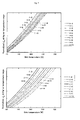
- legend labels are indicated as (atomic % of Al in the well layers)-(atomic % of Al in the barrier layers).
- Figures 7a and 7b indicate the heat sink temperature
- the vertical axes indicate normalized threshold current density J th in high temperature range, where the normalization was carried out such that it becomes 1 for compositions when the (well layers 10W)/(barrier layers 10B) compositions are GaAs/Al 0.15 Ga 0.85 As, at 4 K. Therefore, each curve has been obtained by plotting the threshold current density J th at the second step, after the above-mentioned simulation was carried out for each composition.
- Figure 8 is a graph showing composition dependency of maximum operating temperature T max read from the numerical calculation prospects in Figure 7 .
- Figure 8 has been obtained by conducting the above-mentioned simulation steps through the third step, and plotting values of temperature T max for respective compositions, where the values of temperature T max yield the maximum current density J max in Formula 5 for the allowable current density of the THz-QCL element 1000. It is to be noted that, since J max does not depend on the composition and temperature it will be indicated as a straight line with J max .
- Figure 8 is a graph of composition dependence of operating temperatures read from Figure 7 on assumption that the threshold current density J th is constant in Figure 7 .
- the THz-QCL element 1000 has been actually fabricated and its performance has been measured for several conditions.
- FIGS 9 and 10 are schematic diagrams of an element structure at each step in manufacturing of THz-QCL element 1000 in the embodiment.
- the semiconductor superstructure 100A indicated in Figure 1b is formed by coherent crystal growth on underlying crystal for each manufacturing step by molecular beam epitaxy (MBE) apparatus.
- MBE molecular beam epitaxy
- a single crystal GaAs substrate of orientation (100) is adopted for the substrate 50.
- the ES layer 60 ( Figure 1b ) is formed.
- the ES layer 60 is a layer with sufficient thickness, or 600 nm thick deposited layer of Al 0.5 Ga 0.5 As, as a layer enough resistive against etchant used when the substrate 50 is removed by etching later.
- the highly doped GaAs layer 120 is formed. In so doing, its electron density is controlled to ⁇ 3x10 18 cm -3 by way of doping.
- the active layer 10 is formed.
- the active layer 10 is formed to have stacked structure of the unit structures 10U in Figure 1c .
- Compositions for the barrier layers 10B and the well layers 10W are adjusted for respective samples.
- the thicknesses of the layers are also adjusted to respective samples since the thicknesses are also re-designed according to the compositions of the barrier layers 10B and the well layers 10W.
- the barrier layer 10B1 through the well layer 10W4 in Figure 1c are deposited, in particular, with thicknesses of 9.4/2.4/14.8/3.8/6.4/2.4/7.8/5.4 (nm) in this order.
- the highly doped GaAs layer 140 is formed with 50 nm thickness.
- the electron density is controlled to ⁇ 5x10 18 cm -3 by doping.
- the delta-dope GaAs layer 160 which becomes a contact layer, is formed.
- the delta-dope GaAs layer 160 consists of ten combined sets of 1 nm thick GaAs layer and a delta-dope layer. Then 5 nm thick low temperature grown GaAs layer (LTG-GaAs layer) 180 is formed. Thereafter, the metal layer 30A is formed as indicated in Figure 9a .
- the metal layer 30A is formed, in the order of deposition, as Ta (20 nm)/Cu (600 nm)/Au (100 nm).
- the receptor 40 having metal layer 30B formed thereon is provided.
- the metal layer 30B is formed to have similar structure to the metal layer 30A on the receptor 40 side.
- the substrate 50 is removed by wet etching.
- selective etching is carried out.
- the substrate 50 is removed, and the ES layer 60 is exposed to the surface as in Figure 10g .
- the electrode 20 is formed on the surface of the highly doped GaAs layer 120 of the semiconductor superlattice 100A ( Figure 10i ).
- the electrode 20 is formed with Au of around 100 nm thickness that is patterned to have 200 micrometer width.
- the electrode 20 is used as a mask when removing periphery part of the semiconductor superlattice 100A by dry etching with chlorine gas to obtain QCL structure 100 with a mesa of 200 micrometer width, and a cavity with length of 0.5-1.5 mm is formed by cleaving ( Figure 10j ).
- the operable THz-QCL element 1000 is fabricated ( Figure 10k ).
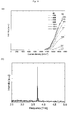
- Figure 11 is a graph showing the measurement results of the samples of the practical fabrication example.
- Figure 12 is a graph showing characteristics of samples (exp.) regarding practical fabrication example having structure of GaAs/Al x Ga (1-x) As for several aluminum composition x, and theoretical calculation prospects (sim.).
- the theoretical calculation scheme adopted in predicting the performances of the THz-QCL element 1000 can serve as a framework in explaining the relationship between the threshold current density J th and the operating temperature. That is, by comparing normalized threshold current densities J th for the same operating temperature in the actually measured data, it has been confirmed that the threshold current density J th was reduced according to increasing Al amount added. Also, by comparing operational temperatures for identical normalized threshold current densities, it has been confirmed that lasing operation was realized at higher temperature than before.
- the materials in the well layers 10W and barrier layers 10B in the present embodiment as mentioned above are respectively set identical among the well layers 10W1-10W4 and among the barrier layers 10B1-10B4, the present invention is not limited to such combination of materials. It should be noted that, although the materials in the well layers 10W and barrier layers 10B in the present embodiment set forth above are respectively set identical among the well layers 10W1-10W4 and among the barrier layers 10B1-10B4, the present invention is not limited to such combination of materials.
- the THz-QCL element 1000 of the present embodiment can be modified to further specific configuration without departing the spirit of the present invention set forth herein.
- ranges for x and y in the composition Al x Ga 1-x As/AlyGa 1-y As (x ⁇ y ⁇ 1) of the (well layers 10W)/(barrier layers 10B) are not specifically limited except that they should satisfy x ⁇ y ⁇ 1.
- both x and y may be set closer to 1 as much as possible, considering the LO-phonon energy E LO as stated above.
- the upper limit of x is set to a value smaller than 1 by a difference amount that is necessary to produce the potential barriers.
- y since y does not have such an upper limit, most typically, y may be set to 1, or 100%.
- the technological concept that has been described in detail along with the THz-QCL element 1000 adopting material base of GaAs in the present embodiment can also be applied to other QCLs adopting other base material.
- QCLs with InP type compound semiconductor will be described for such variation.
- the InP base QCLs have been fabricated recently in bound-to-continuum type. Therefore, it is not easy to predict the threshold current density J th , or to predict the maximum operating temperature T max . This is because electron-electron scattering determines relaxation time in the bound-to-continuum type. As a result, merely considering LO-phonon energy and its scattering is insufficient for predicting the threshold current density J th and the maximum operating temperature T max , and thus the outcome cannot be predicted in such a straight forward manner.
- the maximum operating temperature T max is 115 K for bound-to-continuum type QCLs of THz range having conventional material system of InP/InGaAs/InAlAs. It can be said that, when operating a QCL fabricated with this material system based on the approach of the electron depopulation by the LO-phonon, increasing the content of Al would reduce the threshold current density J th and increase the maximum operating temperature T max .
- THz-QCLs with reduced threshold current density J th or THz-QCLs with raised maximum operating temperature T max are provided. These THz-QCLs are applicable to instruments that use an electromagnetic wave source of THz range.
Landscapes
- Physics & Mathematics (AREA)
- Optics & Photonics (AREA)
- Chemical & Material Sciences (AREA)
- Engineering & Computer Science (AREA)
- Nanotechnology (AREA)
- Condensed Matter Physics & Semiconductors (AREA)
- General Physics & Mathematics (AREA)
- Electromagnetism (AREA)
- Life Sciences & Earth Sciences (AREA)
- Biophysics (AREA)
- Crystallography & Structural Chemistry (AREA)
- Semiconductor Lasers (AREA)
Abstract
Description
- The present invention relates to a quantum cascade laser element. More specifically, the present invention relates to a quantum cascade laser element that emits electromagnetic waves in THz range.
- Recently, a quantum cascade laser, hereinafter called as a "OCL", is gathering much attention as a solid state light source that emits electromagnetic waves in mid infra-red range or in terahertz (THz) range. Having both properties of a light and a radio wave at a time, electromagnetic waves in THz range in particular feature such high resolution capability as a light and such high transmission capability as a radio wave, with milder impact on examined objects than X rays or the like. From these points, electromagnetic waves in THz range are expected to be utilized in applications for, such as, substance identification and human body scanning examination by wave transmission.
- Typical emission mechanism of QCLs utilizes a semiconductor superlattice, which uses potentials only by electrons' conduction bands having an alternating structure of wells and barriers, for example. In short, stimulated emissions by way of intersubband transition are provoked among the subbands that are created in the semiconductor superlattice. The emission mechanism in QCLs is significantly differ from one in conventional semiconductor lasers in this respect, in which stimulated emissions of electromagnetic wave are provoked by way of recombination of an electron and a hole across an energy gap between a conduction band and a valence band. Specifically, QCLs use a potential in a semiconductor superlattice with wells and barriers, and, by applying a voltage thereto, the potential is inclined along thickness direction of the semiconductor superlattice while having well/barrier undulating patterns. The inclined patterned potential is then used to provoke stimulated emissions by electrons in a multi stage manner, or in a cascade scheme. To fabricate a semiconductor superlattice that is capable of such transitions, it is necessary to conduct "band engineering" in which thicknesses of well and barrier layers are precisely designed in consideration of the inclination due to the electric field. In CLs, repeated use of conduction carriers, or electrons, enables a carrier recycling.
- In QCLs, it is possible to cause lasing operation with a wavelength that has no relationship at all with an energy gap of material for the semiconductor superlattice, and on top of that, the lasing wavelength can be tuned through designing process of the semiconductor superlattice. For these reasons, QCLs have been made for emission of electromagnetic waves emitters in THz range, for which wavelength no solid state light source was devised. Such QCLs in the THz range, or hereinafter called "THz-QCLs", have been classified into several types in view of schemes to make population inversion for lasing. One example of THz-QCLs is called "bound-to-continuum" type, in which the electromagnetic wave is emitted by electrons that make transition from an isolated level to a miniband that forms a continuum band. A THz-QCL of this type is disclosed in Non-Patent
Document 1, in which the THz-QCL operates at an oscillation frequency of 3.65 GHz, where the population inversion is created by relaxing electrons in a lower lasing level by way of electron-electron scattering within the miniband. It should be noted that THz-QCLs of bound-to-continuum type may have high voltage efficiency; however, such THz-QCLs need complicated designing and suffer from significant adverse effects of scattering by LO-phonon. - Another type of THz-QCLs is disclosed in Patent Document 1 (
U.S. Patent No. 6,829,269 ). The THz-QCL disclosed inPatent Document 1 uses three electronic levels per one stage of stimulated emission. That is, one additional electronic level is adopted to form population inversion between an upper lasing level and a lower lasing level that need the population inversion for lasing operation. The THz-QCL inPatent Document 1 adopts an upper lasing level (|3>, referred to as "level L3" in the present specification), a lower lasing level (|2>, "level L2"), both of which are related to the lasing operation, and another level (|1>, "level L1") located below the level L2. The level L1 operates to depopulate electrons from the level L2 by using longitudinal optical phonon ("LO-phonon"), (see for example,FIG.3 in Patent Document 1). Such a three-level scheme is hereinafter called "LO-phonon assist type". -
Patent Document 1 discloses a THz-QCL of the LO-phonon assist type that has a semiconductor superlattice provided with repeating structures in its active region for stimulated emissions, where each structure, hereinafter called simply as "unit structure," is configured to realize each stage of stimulated emission. The unit structure includes an emission region and an injection region. Energy potentials, or a band, in the unit structure have been engineered in such a way that the emission region improves the emission efficiency and that the injection region helps formation of the population inversion. In the active region of LO-phonon assist type THz-QCLs, well layers are made of GaAs, whereas barrier layers are made of AlxGa1-xAs to implement such design. - Patent Document 1:
U.S. Patent No. 6,829,269 -
- Non-Patent Document 1: G. Scalari, N. Hoyler, M. Giovannini, and J. Faist, Appl. Phys. Lett. No.86, 181101 (2005)
- Non-Patent Document 2: S. Kumer, Q. Hu, and J. Reno, Appl. Phys. Lett. No.94, 131105 (2009)
- Non-Patent Document 3: T. T. Lin, K. Ohtani, and H. Ohno, Applied Physics Express, No.2, 022102 (2009)
- Among THz-QCLs, ones in LO-phonon assist type as disclosed in
Patent Document 1 generally show good performance. For example, a demonstration of lasing operation at 186 K, which is considered a relatively high temperature for THz-QCLs, is reported for the LO-phonon assist type (Non-Patent Document 2). Moreover, the LO-phonon assist type ones have a relatively simple structure in the semiconductor superlattice. - However, LO-phonon assist type THz-QCLs still need further improvement. So long as the highest temperature for actual lasing operation (hereinafter referred to as a maximum operating temperature Tmax) is nothing more than 186 K, it is necessary to provide a large scale cooling system for lasing operation. If the maximum operating temperature Tmax were raised to 230 K or higher, electronic cooling, such as by a Peltier element, would be sufficient for the lasing operation, which should lead to a significant improvement on usability of the QCLs. It should also be noted that QCLs with raised maximum operating temperature Tmax usually show a reduced threshold current density for lasing (herein after called as "threshold current density Jth") in a temperature range below the maximum.
- Accordingly, the present invention is devised for solving such problems. That is, by reducing the threshold current density Jth, or by raising the maximum operating temperature Tmax, for THz-QCLs, the present invention contributes to practicing various applications that adopt THz-OCLs.
- The inventors of the present application have designed the structures for THz-QCLs such that they have reduced threshold current density Jth for lasing, which reduction should be in direct relationship with the operating temperature, and such that they have raised maximum operating temperature Tmax. Also, the inventors estimated their performances based on a numerical calculation based on theory (theoretical calculation). Moreover, it has been confirmed experimentally that changing material of barrier layers from GaAs, which was the only material adopted therefor, to another material gives good agreement with the prospects of the theoretical calculation. Furthermore, the inventors of the present application have obtained a knowledge from the theoretical calculation that changing material of well layers, from only GaAs to another material results in reduced threshold current density Jth or raised maximum operating temperature Tmax, in THz-QCLs. The present invention has been made as outlined above.
- Accordingly, in one aspect of the present invention, provided is a quantum cascade laser (QCL) element comprising a pair of electrodes and a semiconductor superlattice sandwiched by the pair of electrodes, wherein the semiconductor superlattice has an active region that emits electromagnetic waves of THz range when an voltage is applied between the pair of electrodes, wherein the active region has repeating unit structures, each unit structure having a thickness and including sets of a well layer and a barrier layer alternatingly laminated with each other, and wherein the well layer is made of AlxGa1-xAs (where 0<x<1), which is a mixed crystal of AlAs and GaAs.
- Throughout the present application, an electromagnetic wave in THz range generally denotes an electromagnetic wave in a frequency range of 0.1 THz - 30 THz, or in a wavelength range of 10 µm - 3 mm. Also through description in the present application, the element structure or its function may be described in technical terms that are diverted or borrowed from optical technologies covering visible lights or infra-red rays, in accordance with the customary usage in the art of the present application. Therefore, although generated electromagnetic waves are those of far different frequency or wavelength range from ones for visible lights, such terms as "laser" or "luminescence" may be used, and such terms as "optical- " or the like may also be used to describe elements of quantum cascade lasers or to describe phenomena of the stimulated emissions.
- Any of the embodiments of the present invention provides a THz-QCL with reduced threshold current density Jth, or with raised maximum operating temperature Tmax than before. Accordingly the present invention contributes to developments of devices that use an emitting source of electromagnetic waves in THz range.
-
-
Figure 1 is a perspective view (Figure 1a ), an enlarged cross sectional view (Figure 1b ), and a further enlarged partial cross sectional view (Figure 1c ), showing general structure of a THz-QCL element in an embodiment of the present invention. -
Figure 2 is a schematic diagram for illustrating a potential for electrons and subbands of electrons in a unit structure of a QCL structure formed in a THz-QCL element for an embodiment of the present invention. -
Figure 3 is a schematic diagram for illustrating phonon mediated leak of thermally excited electrons in an embodiment of the present invention. -
Figure 4 is a schematic diagram for illustrating thermal backfilling in an embodiment of the present invention. -
Figure 5 is a schematic diagram of energy dispersion relationships in xy plane.Figure 5a depicts an energy dispersion relationship for conventional design; whereasFigure 5b depicts an energy dispersion relationship for the embodiment of the present invention. -
Figure 6 is an energy chart for illustrating relaxation mechanisms of electrons. -
Figure 7 is a detailed graph of numerical calculation prospects on threshold current density Jth while composition of an active region is changed. -
Figure 8 is a graph showing composition dependency of maximum operating temperature Tmax read from the numerical calculation prospects in an embodiment of the present invention. -
Figure 9 is a schematic diagram of element structure at each step through fabrication of a THz-QCL element in an embodiment of the present invention. -
Figure 10 is a schematic diagram of element structure at each step through fabrication of a THz-QCL element in an embodiment of the present invention. -
Figure 11 depicts current emission characteristics (Figure 11a ) and a spectrum of electromagnetic wave emissions (Figure 11b ) obtained from an actually operated sample with x = 0.15 in GaAs/AlxGa(1-x)As for well layer/barrier layer compositions in a THz-QCL element in an embodiment of the present invention. -
Figure 12 is a graph showing characteristics obtained from a sample (exp.) and theoretical calculation prospects (sim.) corresponding to practical fabrication examples having structure of GaAs/AlxGa(1-x)As with changing aluminum composition x, in an embodiment of the present invention. - Embodiments of the present invention will be described. For all drawings, the common reference signs are given to common parts or elements unless otherwise noted. Moreover, each element in the drawing should be understood as not being drawn to scale.
- In the first place, what will be described are operation mechanisms in quantum cascade laser elements (THz-QCL elements) of LO-phonon assist type that emit electromagnetic waves in THz range, and principles for their improvements in the present embodiment.
-
Figure 1 is a perspective view (Figure 1a ), an enlarged cross sectional view (Figure 1b ), and a further enlarged partial cross sectional view (Figure 1c ), showing general structure of a THz-QCL element 1000 in the present embodiment. A typical THz-QCL element 1000 (Figure 1a ) is generally equipped with a pair ofelectrodes QCL structure 100 that is a semiconductor superlattice formed therebetween. Theelectrodes QCL structure 1000 and an electric current for emission, or luminescence. Theelectrodes QCL structure 100 includesactive region 10. The THz-QCL element 1000 can operate in such a way thatelectromagnetic waves 2000 of THz range is emitted by transition of electrons from one subband to another subband located below in energy, where both subbands are formed in theactive region 10 when an electric voltage is applied between the pair ofelectrodes electrode 30 is formed on receptor substrate 40 (hereinafter referred to as "receptor 40") in the THz-QCL element 1000 inFigure 1 . - For the purpose of the operation mentioned above, the active region 10 (
Figure 1b ) hasunit structures 10U that are provided in a layered manner along the thickness direction, where eachunit structure 10U has alternatingly stacked sets of awell layer 10W and abarrier layer 10B. The well layers 10W consist of AlxGa1-xAs (where 0<x<1), whereas the barrier layers 10B, in the present embodiment, consist of AlyGa1-yAs (where x<y≤1), which is a mixed crystal of AlAs and GaAs. Because of the setting x<y, potentials formed by the conduction band of barrier layers 10B create potential barriers for the conduction band inwell layers 10W. It should be noted that eachunit structure 10U has a plurality of suchwell layers 10W and a plurality of such barrier layers 10B. Accordingly, when each ofbarrier layers 10B is to be identified as necessity, they may be distinguished as barrier layers 10B1-10B5 in this order from thesubstrate 50. Similarly, the well layers 10W may be distinguished as well layers 10W1-10W4. - The QCL structure 100 (
Figure 1a ) is formed by trimming off the extended periphery portion from layered structure for thesemiconductor superlattice 100A. In thesemiconductor superlattice 100A, an etch stop layer 60 ("ES layer 60") is formed onGaAs substrate 50 having surface orientation (001) (hereinafter, "substrate 50") by disposing AlGaAs with 600 nm thickness. Details for theES layer 60 will be described later. Then, a highly doped n-type GaAs layer 120 (electron density ∼3x1018 cm3) is formed with 800 nm thickness on the surface of theES layer 60; thereafter, anactive region 10 is formed. On the surface of the formedactive region 10, a highly doped n-type GaAs layer 140 (electron density ∼3x1018 cm3) is formed with 50 nm thickness. Then a delta-dope GaAs layer 160 consisting of ten sets of 1 nm thick GaAs layer and a delta-dope layer of Si is formed; and lastly, a low temperature grown GaAs layer (LTG-GaAs layer) 180 is formed with 5 nm thickness. It should be noted thatFigure 1b indicates the stacked film structure formed on one surface of asubstrate 50 in the order of the stacking process, from the bottom to the top in the drawing. Thesemiconductor superlattice 100A inFigure 1b is indicated in upside down view of theQCL structure 100 inFigure 1a . - In the conventional THz-QCL elements, not shown, the
active region 10 of theQCL structure 100 is fabricated such that the well layers 10W are made of GaAs, and the barrier layers 10B are made of AlxGa1-xAs (x is 0.15, 0.20, or the like). See for example,Patent Document 1, column 31. In contrast, the THz-QCL element 1000 in the present embodiment is fabricated in such a manner that, with the addition of Al also to the well layers 10W, the well layers 10W are made of AlxGa1-xAs (0<x<1), and the barrier layers 10B are made of AlyGa1-yAs (x<y≤1). - In the
semiconductor superlattice 100A inFigure 1b , theunit structures 10U are formed in a layered manner of, such as, 10-200 stacks in theactive region 10.Figure 1c indicates with enlarged view the structure of one unit, or one period, for eachunit structure 10U. Theunit structure 10U has the barrier layers 10B and well layers 10W alternatingly layered with each other. Since eachbarrier layer 10B and each well layer 10W are stacked alternatingly, the well layer 10W1 is disposed directly on the barrier layer 10B1, and the barrier layer 10B2 is disposed directly on the well layer 10W1. The rest is the same as the above. It should be noted that the barrier layer 10B5 is corresponding to barrier layer 10B1 in aunit structure 10U in the next period. -
Figure 2 is a schematic diagram for illustrating a potential for electrons and subbands of electrons in theunit structure 10U of theQCL structure 100 formed in the THz-QCL element 1000.Figure 2a shows a variation of potential for electrons in z-axis direction. The potential is generally inclined due to the voltage for operation applied to the THz-QCL element 1000. Reference signs corresponding to respective layers in theunit structure 10U are indicated inFigure 1c for respective protrusion and recess portions of the potential. Moreover,Figure 2b is a schematic diagram of a dispersion relationship, which indicates energy levels of electrons in theunit structure 10U with reference to a wave number (k) space in the xy plane (Figure 1 ). -
Figure 2a depicts, in addition to the potential, five curves for |Ψ|2, which is squared amplitude of z dependent factor of a three dimensional wave function Ψ for an electron. Each curve shows relative values of probability of finding an electron at each position along z-axis obtained by conducting self-consistent calculation. The depicted five curves are: a curve |Ψ3|2 corresponding to the level L3, and curves |Ψ2|2 and curves |Ψ1|2 corresponding respectively to levels L2 and L1. Two curves are indicated for each of levels L2 and L1 because there are two wave functions with degenerated energy values for each. In this respect, electrons in levels L1-L3 have energy dispersion relationships as indicated inFigure 2b , for their wave number (k) space in plane with the xy plane (Figure 1 ). The levels L3 and L2 are the upper and lower lasing levels respectively, whereas the level L1 is the depopulation level. It should be noted that vertical positions of curves |Ψ3|2, |Ψ2|2, and |Ψ1|2 on the drawing are depicted in such a manner that each axis for denoting |Ψ|2 = 0 (or baseline for each curve, not shown) reflects corresponding energy eigen value at kx = ky = 0 inFigure 2b , or a minimum value of energy for corresponding level. - The THz-
QCL element 1000 provided with theQCL structure 100 having the structure and the potential profile mentioned above operates as follows. In eachunit structure 10U, electromagnetic waves in THz range are emitted by stimulated emission, when electrons make transition from the upper lasing level or the level L3, to the lower lasing level or the level L2. The electromagnetic waves are indicated by a wavy arrow inFigure 2 . To form the population inversion for lasing, the details in the structure of theunit structure 10U, or thicknesses and orders for respective layers as well as the value of the potential, are designed such that electrons in the level L2 can be efficiently depopulated to the level L1. - To give an explanation of the emission process by focusing on the electron's action, the electron makes transition from the level L3 to the level L2, where both levels have significant probability of finding an electron in the well layer 10W4 or 10W3. During the transition, electrons couple to the optical field there and emit electromagnetic waves, or making nonradiative transition. The level L2, which is the level of the electron after transition, has significant probability of finding electron also in the well layer 10W2. Therefore, an electron at the level L2 may tunnel through the barrier 10B3. The electron at the level L2 experiences electron-phonon scattering with LO-phonons and makes transition to the level L1 mainly within the well layer 10W2. Then, the electron at the level L1 is injected to level L3, not shown, of a
unit structure 10U located the next position in a negative z-axis direction. Thus, the areas of the well layers 10W4 and 10W3 may be considered as emission areas where electromagnetic waves are radiated. Also, the well layer 10W2 acts as a phonon well layer where depopulation of electrons is enhanced by use of LO-phonon scattering from the electron distribution at the level L2. Moreover, thewell layer 10W acts as an injection well layer, which is an injection area for electrons in the level L1 toward aunit structure 10U in the next stage. - The inventors have analyzed mechanisms governing the threshold current density Jth and the maximum operating temperature Tmax in THz-QCLs of LO-phonon assist type, and have found that, in addition to the depopulation effect of electrons from the level L2 to the level L1, other effects by LO-phonons are brought about. Specifically, the maximum operating temperature Tmax and the threshold current density Jth are influenced by the following two effects.
- One is a mechanism called phonon mediated leak of thermally excited electrons.
Figure 3 is a schematic diagram illustrating the phonon mediated leak of thermally excited electrons.Figure 3 depicts a chart of electronic energy levels in theunit structure 10U similarly indicated as inFigure 2b . To realize lasing with minimum electric current or in maximum temperature setting, it is preferable as indicated inFigure 3 that electromagnetic wave emissions with transition to the level L2 should be contributed by as many electrons in the level L3, which is the upper lasing level, as possible. However, in the actual situation, another transition mechanism related to LO-phonons causes a nonradiative transition, in which electrons make transition from the level L3 to the level L2 without emission at all. This nonradiative transition is associated with electrons that are thermally excited to have higher energy than a certain level out of all the electrons in the level L3. Due to the thermal excitation, the electron in the level L3 inFigure 3 also moves in xy plane with non-zero wave number k, thus it is possible that the electron may have an energy value higher than the minimum energy E3 by amount of its kinetic energy. The degree of such thermal excitation is expressed as kB Telectron, where Telectron denotes electronic temperature, and kB denotes Boltzmann constant. As an example value, kB Telectron is around 8.6 meV in the case of the Telectron is 100 K. In such a case, the difference E32 between the minimum energy E3 of the level L3 and the minimum energy E2 of the level L2 corresponding to a photon energy of the emitted electromagnetic wave is around 15 meV as an example. The LO-phonon energy ELO for a substance with a composition of almost entirely GaAs is around 36 meV. Therefore, in the course of the operation, there will be a large number of electrons in the level L3 having energy value of the same or higher than an energy value of E2+ELO that is higher than the baseline indicating the minimum energy E2 of the level L2 by an amount of energy ELO, the LO-phonon energy, which are indicated by hatching in the drawing. Moreover, the number of such electrons will increase according to the electronic temperature Telectron. - Furthermore, electrons exceeding E2 + ELO interact with LO-phonon and relax to the level L2 without emission with extremely high rate (nonradiative transition). This is caused due to the nature of LO-phonons. When such nonradiative transition prevails, the population inversion formed between the level L3 and level L2 due to the depopulation of electrons will be cancelled, and lasing will be impeded. This phenomenon of nonradiative transition of thermally excited electrons due to the LO-phonon is the phonon mediated leak of the thermally excited electrons. That is, the phonon mediated leak of the thermally excited electrons is a mechanism through which thermally excited electrons in the level L3 make nonradiative transition or "leak", without making optical transition.
- The other effect of LO-phonons is one in which electrons are thermostatistically excited from the level L1 to the level L2, and such electrons cancel the population inversion. This phenomenon is called thermal backfilling.
Figure 4 is a schematic diagram illustrating the thermal back-filling. This mechanism reflects the fact that electrons depopulated from the level L2 to the level L1 probabilistically include electrons having more energy than energy difference E21, which is a difference value between the minimum energy values E2 and E1 of the levels L2 and L1 respectively. The energy difference E21 is set almost the same as, or slightly smaller (such as, by 1 meV or less) than the energy ELO, in consideration of the mechanism of the depopulation of electrons by the LO-phonon. - To suppress the phonon mediated leak of the thermally excited electrons, the inventors of the present application have paid attention on modification of materials of the
QCL structure 100 for changing the value of the LO-phonon energy ELO. More specifically, the material of theQCL structure 100 is selected in such a way that the following expression is satisfied:
when an electric voltage is applied for emission operation of electromagnetic waves. In this expression, ELO denotes energy of an LO-phonon that can be excited within thesemiconductor superlattice 100, E32 denotes a difference value between the minimum energy E3 of the upper lasing level and the minimum energy E2 of a lower lasing level, or E3 - E2, and T denotes operating temperature (unit:K). - More preferably, the materials of the
QCL structure 100 is selected to satisfy the following expression: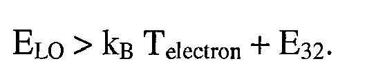
In this expression, Telectron denotes electronic temperature (unit:K). In these material selections, the probability of mediation, with which the electrons thermally excited in the level L3 or the upper lasing level make the nonradiative transition from the level L3 to the level L2 or the lower lasing level, is reduced. In this regard, the probability for the electron of leaking from the level L3 to the level L2 with the nonradiative transition is further reduced according to increase of the value of LO-phonon energy ELO. Moreover, when the value of the ELO is increased, the leak through the nonradiative transition is prevented even for greater kB Telectron value as an indication of the thermal excitation. Consequently, if the value of ELO is increased, the maximum operating temperature Tmax of the above-mentioned QCL will be raised. - It should be noted that the electronic temperature Telectron is higher than the operating temperature T by around 10 - 20 K or the like. This is because, in laser elements in pulse operation or continuous operation, supplied electric energy is transmitted first to electrons, and the thermal energy of the electrons are then transferred, or dissipated, to heat sink or so. Since the electronic temperature Telectron becomes higher than the operating temperature T, which can be measured from outside, the ELO is determined by a comparison with the operating temperature T, and more preferably determined by a comparison with the electronic temperature Telectron.
- Merely increasing the value of LO-phonon energy ELO as described above does not have any specific impact on the thermal backfilling. This is because the LO-phonon energy ELO does not have direct influence on the electrons excited from the level L1 to the level L2. However, the influence of the thermal backfilling can be reduced when the energy difference E21 between the minimum energy for the level L2 and one for the level L1 is maintained such that these minimum energy values satisfy a condition for favorably practicing the depopulation of electrons with the LO-phonon energy ELO from the level L2 to the level L1. Specifically, since the thermal backfilling is caused by thermal excitation of electrons from the level L1 to the level L2, modifying the design of the
QCL structure 100 to have increased E21 in response to the increase of ELO will also lead to reduction of the thermal backfilling. - To reflect the concepts of the improvements in the present embodiment described above, the materials making the
active region 10 in theQCL structure 100 are modified from those adopted before, as a solution of increasing the LO-phonon energy ELO. Also, the design of theQCL structure 100 is modified or adjusted accordingly. - A specific solution of the present embodiment is to increase aluminum (Al) in the
active region 10 to increase the energy ELO. That is, to increase the LO-phonon energy ELO, Al is increased for the combination of GaAs only composition (for conventional well layer) and Al0.15Ga0.85As or similar composition (for conventional barrier layer), where Al0.15Ga0.85As is a composition of mixed crystal of GaAs and AlAs containing 0.15 of Al in atomic ratio. The LO-phonon energy for GaAs is about 36 meV, and the LO-phonon energy for GaAs/Al0.15Ga0.85As in the (conventional well layer)/(conventional barrier layer) composition is also about 36 meV. In contrast, the LO-phonon energy for AlAs is about 44 meV. Moreover, in theactive region 10, Al content is increased in the barrier layers 10B and in the well layers 10W too. In particular, providing aluminum Al into the well layers 10W is effective, because the well layers 10W occupy greater fraction in theunit structure 10U as shown inFigure 2a , and the provision of aluminum Al to the well layers 10W makes it possible to set the LO-phonon energy closer to -44 meV. Therefore, in theactive region 10 of the THz-QCL element 1000 in the present embodiment, by introducing aluminum Al to the well layers 10W in particular, the LO-phonon energy is increased than before. - In the THz-
QCL element 1000 in the present embodiment, in addition to increasing Al in theactive region 10, its design is also modified or adjusted from that in conventional one.Figure 5 is a schematic diagram of energy dispersion relationships in xy plane.Figure 5a depicts an energy dispersion relationship for conventional design, whereasFigure 5b depicts one for the present embodiment. Although such details as effective mass of electron in each level may be varied according to the modification of materials, they are not reflected in the drawings. As can be seen from the comparison ofFigure 5b withFigure 5a , the design will be changed in the THz-QCL element 1000 to have expanded difference between the levels L2 and L1 in response to the increased energy ELO for the material modification. - That is, the probability of the depopulation from the level L2 into the level L1 is set increased is increased to implement population inversion necessary for the laser oscillation. Typically, the
QCL structure 100 is configured in such a manner that the difference E21 between the minimum energy values E2 and E1 for the levels L2 and L1 satisfies, when a voltage is applied, a relationship - E21 ≥ ELO
- Further description will be made in this respect with reference to
Figure 6. Figure 6 is an energy chart for illustrating relaxation mechanisms of the electrons.Figure 6a depicts a case when the well/barrier layers have compositions of GaAs/Al0.15Ga0.85As, assuming the energy ELO is about 36 meV; whereasFigure 6b depicts a case when the well/barrier layers have compositions of AlxGa1-xAs/AlyGa1-yAs (x<y≤1), assuming the energy ELO is about 44 meV. The energy ELO may vary for example from -36 meV to -44 meV in response to values specified for the above-mentioned x and y. The minimum energy E1 of the level L1 refers to an energy value for two degenerated levels as indicated inFigure 2a . Also, indications of lifetime for the transitions are placed between the levels where the transitions take place. The illustration is indicated for a case when energy of 15 meV, corresponding to photon energy of 3.6 THz electromagnetic wave, is provided between the levels L3 and L2. For the purpose of explanation, E21, or E2 - E1 is assumed to be identical to ELO. - When the well/barrier layers have compositions of GaAs/Al0.15Ga0.85As as indicated in
Figure 6a , electrons having 21 meV higher energy than the minimum energy E3 of the level L3, i.e., electrons thermally excited to an extent that associated electronic temperature Telectron reaches around 240 K, mostly make nonradiative transition to the level L2. In other words, the margin to upper boundary of an energy range over which electrons can be distributed is 21 meV above the E3. In contrast, for AlxGa1-xAs/AlyGa1-yAs (x<y≤1) as indicated inFigure 6b , the upper limit mentioned above is located 29 meV above the minimum energy E3 of the level L3, which expands the margin to upper boundary available for the electronic temperature Telectron by about 8 meV, or 90 K for the energy ELO of 44 meV. Even though GaAs is not entirely replaced by AlAs, addition of Al to GaAs provides additional margin against the phonon mediated leak for the thermally excited electrons. This is a countermeasure against the phonon mediated leak of the thermally excited electrons. - On top of that, the effect of the thermal backfilling is also alleviated by introducing Al to GaAs for modifying or adjusting the design of the
semiconductor superstructure 100A. Assuming that E21 = ELO is satisfied and that the electronic temperature Telectron is 200 K, if the energy ELO is 36 meV, around 11 % of electrons in the level L1 make transition to the level L2 with thermal excitation. In contrast, for energy ELO of 44 meV, the fraction of electrons in the level L1 that will make transition to the level of L2 is reduced to around 7.3%. It follows that, according to the shift of the ELO from 36 meV to 44 meV, the number of electrons in the level L2 relating to the thermal backfilling becomes 1/1.5 as many electrons as before, which makes it easier to generate population inversion. - Furthermore, our acquired knowledge includes the fact that scattering probability of the thermally excited electrons by LO-phonons is not increased even when the material composition was modified for the purpose of the increasing the LO-phonon energy. That is, in the case the scattering probability increases according to the above-mentioned material modification, usually the possibility of reduction of τ32 should be taken into account. However, the inventors of the present application have confirmed that such increase of scattering probability per se does not happen at al.
- It should be noted that there is no limitation on specific solutions for implementing the design modification indicated with reference to
Figures 5b and6b . The design can be modified, for example, by adjusting voltages applied for operation, and by adjusting thicknesses for the well layers 10W and the barrier layers 10B. - The inventors of the present application assessed though theoretical calculation as to whether the maximum operating temperature Tmax is increased as intended or not, and as to whether threshold current density Jth is reduced or not, after modifications of the materials and the design, mentioned above.
- Parameters used for the rate equation have relationship with Jth as follows:

Here, ε0 is the dielectric constant of vacuum, e is charge of an electron, Γ is an optical confinement factor, Z32 is a dipole matrix element between the levels L3 and L2, λ is a wavelength of the electromagnetic wave in vacuum, n is a refractive index for the electromagnetic wave with wavelength λ, L is a thickness of theunit structure 10U, αw is a loss of mirror, αM is a loss of cavity, γ32 is a line width, or full width at half maximum, for laser transition between the levels L3 and L2, τ3 is a lifetime of electron in the level L3, τ2 is a lifetime of electron in the level L2, and τ32 is a lifetime for electron in the level L3 to transition to the level L2 through intersubband transition. - For the τ32 found in the expression of the threshold current density Jth in
Formula 1, the following relationship holds.
Here, τe-e is a time constant of electron-electron scattering, or average lifetime, which will be referred to as "scattering time", and τtnermalLO is a scattering time of the phonon mediated leak for thermally excited electrons. For materials in which Al is introduced into GaAs, since the τe-e is long enough to be neglected while the τthermalLO is short, the lifetime from the level L3 to the level L2 is determined by the τthermalLO of the phonon mediated leak for thermally excited electrons. The τthermalLO is given as follows.
Here, τLO is a scattering time of LO-phonon scattering for electrons having kinetic energy of ELO - E32. The τelectron and τLO are fitting parameters to be determined such that the theoretical curve explains experimental results. - Based on the relationship of
Formula 2, in addition to the τ32, temperature dependences of τ31, which is a lifetime of electrons in the level L3 to the level L1, and of τ2 may be crucial. Regarding these temperature dependences, since the LO-phonons obey Bose-Einstein statistics, the following relationship holds.
Here, ℏ(h-bar) is a Planck constant h divided by 2π, ωLO is an angular frequency of LO-phonon. Tlattice is lattice temperature of the crystal. ELO is energy of LO-phonon and is equivalent to h x ωLO. The lattice temperature Tlattice is set to identical value to the heat sink temperature. - The maximum current density Jmax flowing through the THz-
QCL element 1000 is determined by the following relationship.
Here, n is a density of carrier (electron), q is electric charge of the carrier (electron), which is identical to the elementary charge e. Theoretically, the maximum operating temperature Tmax is obtained from a range that has nonnegative Jmax - Jth. That is, the THz-QCL element 1000 can operate only when the threshold current density Jth, which is susceptible to the temperature, does not exceed a maximum current density Jmax that is allowed to flow during lasing operation. - Simulation on the effect of material modification is conducted through the theoretical calculation based on these relation formulas as in the following steps. In the first step, relaxation times τ(τ31, τ21) are calculated under low temperature condition. In doing so, electron-electron scattering is neglected. Then the τLO and the τelectron in the τthermalLO are determined to fit experimental results. Next, in the second step, temperature dependencies for all relaxation times τ(τ31, τ21, τLO) are determined, and the threshold current densities Jth for respective temperature values are numerically calculated. The threshold current densities Jth generally have a tendency to increase according to increase of the temperature. Then, in the third step, temperature Tmax is determined in such a manner that the threshold current density Jth therefrom matches the maximum value Jmax of the current density. More details have been disclosed by a part of the inventors of this application (Non-Patent Document 3: T. T. Lin, K. Ohtani, and H. Ohno, Applied Physics Express, No.2, 022102 (2009)).
- Next, calculated prospects of lasing operation based on rate equations are described. The numerical calculation has been carried out for threshold current density Jth with each temperature in respect of material modifications for cases (1) when Al is added to the barrier layers only, and (2) when Al is added to both the well and barrier layers. This is because, once the threshold current density Jth is obtained for each temperature, not only the composition dependence in the threshold current density Jth, but also knowledge of the maximum operating temperature Tmax will be obtained.
Figure 7 is a detailed graph of numerical calculation prospects of threshold current density Jth when composition of anactive region 10 is shifted. When the modified composition of theactive region 10 is indicated by the (well layers 10W)/(barrier layers 10B) compositions,Figure 7a shows cases when Al content x is changed for x = 0.15 - 0.95 with 0.1 increment, as well as x = 1, for GaAs/AlxGa1-xAs; whereasFigure 7b shows cases when Al content x is changed for x = 0.2 - 0.8 with 0.1 increment, while keeping y = x + 0.2, in AlxGa1-xAs/AlyGa1-yAs. For each graph, legend labels are indicated as (atomic % of Al in the well layers)-(atomic % of Al in the barrier layers). The horizontal axes ofFigures 7a and 7b indicate the heat sink temperature, and the vertical axes indicate normalized threshold current density Jth in high temperature range, where the normalization was carried out such that it becomes 1 for compositions when the (well layers 10W)/(barrier layers 10B) compositions are GaAs/Al0.15Ga0.85As, at 4 K. Therefore, each curve has been obtained by plotting the threshold current density Jth at the second step, after the above-mentioned simulation was carried out for each composition. Also,Figure 8 is a graph showing composition dependency of maximum operating temperature Tmax read from the numerical calculation prospects inFigure 7 .Figure 8 has been obtained by conducting the above-mentioned simulation steps through the third step, and plotting values of temperature Tmax for respective compositions, where the values of temperature Tmax yield the maximum current density Jmax in Formula 5 for the allowable current density of the THz-QCL element 1000. It is to be noted that, since Jmax does not depend on the composition and temperature it will be indicated as a straight line with Jmax. - From the results shown in
Figure 7 , assuming that the normalized threshold current density Jth can be kept constant, it is suggested that the heat sink temperature or operating temperature may be raised according to increase of the Al content. It is also suggested that, on the assumption that the operating temperature is kept constant, the normalized threshold current density Jth is reduced according to increase of the Al content. Moreover,Figure 7b also suggests that adding Al to both the well layers 10W andbarrier layers 10B is advantageous than adding Al only to the barrier layers 10B as inFigure 7a . - Such points are clearly seen also on
Figure 8. Figure 8 is a graph of composition dependence of operating temperatures read fromFigure 7 on assumption that the threshold current density Jth is constant inFigure 7 . - Next, the THz-
QCL element 1000 has been actually fabricated and its performance has been measured for several conditions. - The manufacturing method used for making the practical fabrication examples of THz-
QCL element 1000 will be described.Figures 9 and10 are schematic diagrams of an element structure at each step in manufacturing of THz-QCL element 1000 in the embodiment. First, thesemiconductor superstructure 100A indicated inFigure 1b is formed by coherent crystal growth on underlying crystal for each manufacturing step by molecular beam epitaxy (MBE) apparatus. In this regard, a single crystal GaAs substrate of orientation (100) is adopted for thesubstrate 50. Also, the ES layer 60 (Figure 1b ) is formed. TheES layer 60 is a layer with sufficient thickness, or 600 nm thick deposited layer of Al0.5Ga0.5As, as a layer enough resistive against etchant used when thesubstrate 50 is removed by etching later. Next, the highly dopedGaAs layer 120 is formed. In so doing, its electron density is controlled to ~3x1018 cm-3 by way of doping. Thereafter, theactive layer 10 is formed. Theactive layer 10 is formed to have stacked structure of theunit structures 10U inFigure 1c . Compositions for the barrier layers 10B and the well layers 10W are adjusted for respective samples. The thicknesses of the layers are also adjusted to respective samples since the thicknesses are also re-designed according to the compositions of the barrier layers 10B and the well layers 10W. In an example for them, to reproduce a sample with a conventional structure having Al0.15Ga0.85As for the well layers 10W and GaAs for the barrier layers 10B, which is a sample corresponding to the lowest temperature curve inFigure 7a , the barrier layer 10B1 through the well layer 10W4 inFigure 1c are deposited, in particular, with thicknesses of 9.4/2.4/14.8/3.8/6.4/2.4/7.8/5.4 (nm) in this order. Next, the highly dopedGaAs layer 140 is formed with 50 nm thickness. Regarding the highly dopedGaAs layer 140, the electron density is controlled to ∼5x1018 cm-3 by doping. Then the delta-dope GaAs layer 160, which becomes a contact layer, is formed. The delta-dope GaAs layer 160 consists of ten combined sets of 1 nm thick GaAs layer and a delta-dope layer. Then 5 nm thick low temperature grown GaAs layer (LTG-GaAs layer) 180 is formed. Thereafter, themetal layer 30A is formed as indicated inFigure 9a . Themetal layer 30A is formed, in the order of deposition, as Ta (20 nm)/Cu (600 nm)/Au (100 nm). - Also as indicated in
Figure 9b , thereceptor 40 havingmetal layer 30B formed thereon, is provided. Themetal layer 30B is formed to have similar structure to themetal layer 30A on thereceptor 40 side. - Next, as indicated in
Figure 9c , overall layered structure is completed with wafer bonding, in which themetal layers - Thereafter, as indicated in
Figure 9d , by polishing thesubstrate 50 to 80 micrometer thick, and thereceptor 40 to 20 micrometer thick, and as indicated inFigure 9e , they are coated by thewax 500 except the outer surface of thesubstrate 50. It should be noted that thewax 500 is not depicted inFigure 9a on a side parallel to the sheet of the drawing. - Next, as indicated in
Figure 10f , most part of thesubstrate 50 is removed by wet etching. The wet etching is carried out with etchant of H3PO4:H2O2:H2O = 1:1:1 (in volume fraction), with etchant temperature of 10 degree-C, for 10 minutes or so. Next, selective etching is carried out. The etchant adopted is (citric acid C6H8O7:H2O):H2O2 = 3:1 (in volume fraction), the etchant temperature is 40 degree-C, and the process time is for around 1-3 hours. As a result, thesubstrate 50 is removed, and theES layer 60 is exposed to the surface as inFigure 10g . Thereafter, to remove theES layer 60, selective etching by buffered hydrofluoric acid (HF with NH4F) is carried out. At this stage theES layer 60 is removed and the highly dopedGaAs layer 120 is exposed to the surface of thesemiconductor structure 100A as indicated inFigure 10h . - Furthermore, the
electrode 20 is formed on the surface of the highly dopedGaAs layer 120 of thesemiconductor superlattice 100A (Figure 10i ). Theelectrode 20 is formed with Au of around 100 nm thickness that is patterned to have 200 micrometer width. Theelectrode 20 is used as a mask when removing periphery part of thesemiconductor superlattice 100A by dry etching with chlorine gas to obtainQCL structure 100 with a mesa of 200 micrometer width, and a cavity with length of 0.5-1.5 mm is formed by cleaving (Figure 10j ). Lastly, by establishing electrical connections to theelectrodes QCL element 1000 is fabricated (Figure 10k ). - For the time being, what has been confirmed experimentally is related to only samples having modified composition in barrier layer indicated in
Figure 7a . More specifically, the samples for the practical fabrication example was obtained with varying x in GaAs/AlxGa(1-x)As for x = 0.15, 0.25, and 0.35. - Next, measurements have been made using samples for the practical fabrication example manufactured as described above, concerning the normalized threshold current density Jth in respective temperatures. In addition, theoretical calculation has been carried out in line with the similar scheme of
Figure 7 .Figure 11 is a graph showing the measurement results of the samples of the practical fabrication example.Figure 11 indicates current-emission characteristics (Figure 11a ) and spectrum of emitted electromagnetic waves (Figure 11b ) for an actually operated sample, with x = 0.15 for composition of GaAs/AlxGa(1-x)As for well layer/barrier layers in the THz-QCL element.Figure 12 is a graph showing characteristics of samples (exp.) regarding practical fabrication example having structure of GaAs/AlxGa(1-x)As for several aluminum composition x, and theoretical calculation prospects (sim.). - As indicated in
Figure 11 , the lasing operation of a sample with x = 0.15 in GaAs/AlxGa1-xAs was confirmed, at low temperature of 60 K or below, with the threshold current density of around 1250 A/cm2. In addition, the maximum operating temperature was about 143 K for pulse operation with repetition frequency of 500 Hz. Also, as indicated inFigure 12 , as for the normalized threshold current density Jth, measured results with the practical fabrication example were fairly consistent with the theoretically calculated prospects. Particularly over 60 K temperature range, the measured results in samples and theoretically calculated prospects had great consistency with each other. - It follows that, the theoretical calculation scheme adopted in predicting the performances of the THz-
QCL element 1000 can serve as a framework in explaining the relationship between the threshold current density Jth and the operating temperature. That is, by comparing normalized threshold current densities Jth for the same operating temperature in the actually measured data, it has been confirmed that the threshold current density Jth was reduced according to increasing Al amount added. Also, by comparing operational temperatures for identical normalized threshold current densities, it has been confirmed that lasing operation was realized at higher temperature than before. - It should be noted that the maximum operating temperatures Tmax found in the samples in GaAs/AlxGa(1-x)As are 143 K for x=0.15, 132 K for x=0.25, and 120 K for x=0.35. When only these results are concerned, it cannot be said that increasing A1 addition amount actually raises the maximum operating temperature Tmax so far. The reason why actual samples show such behavior with the maximum operating temperature Tmax is unclear for the time being. However, the inventors of the present application have confirmed that good agreement was found generally between the theoretical calculation prospects and the experimental results. More specifically, it has been confirmed based on the experiment that there was correctness in the theoretical prediction with respect to the possibility of reduction in the threshold current density Jth due to increasing Al addition, at temperature of 100 K or higher. Therefore, we have reason to believe that, based on the theoretical prediction, the maximum operating temperature Tmax is to be increased, by solving difficulties underlying in the experiment. Furthermore, it should be noted that, Al content was increased only for the barrier layers 10B in the experimental results mentioned above. We also believe in this regard that, if experiments are carried out by adding Al also to the well layers 10W and increasing the Al amount added thereto, the threshold current density Jth will be reduced and the maximum operating temperature Tmax will be raised, as suggested by the calculation prospects in
Figures 7b and8b . - It should be noted that, although the materials in the well layers 10W and barrier layers 10B in the present embodiment as mentioned above are respectively set identical among the well layers 10W1-10W4 and among the barrier layers 10B1-10B4, the present invention is not limited to such combination of materials. It should be noted that, although the materials in the well layers 10W and barrier layers 10B in the present embodiment set forth above are respectively set identical among the well layers 10W1-10W4 and among the barrier layers 10B1-10B4, the present invention is not limited to such combination of materials.
- Also, the THz-
QCL element 1000 of the present embodiment can be modified to further specific configuration without departing the spirit of the present invention set forth herein. For example, ranges for x and y in the composition AlxGa1-xAs/AlyGa1-yAs (x<y≤1) of the (well layers 10W)/(barrier layers 10B) are not specifically limited except that they should satisfy x<y≤1. For example, both x and y may be set closer to 1 as much as possible, considering the LO-phonon energy ELO as stated above. However, since the potential barriers of the barrier layers 10B with relative to the well layers 10W are formed by the difference between x and y, the upper limit of x is set to a value smaller than 1 by a difference amount that is necessary to produce the potential barriers. On the other hand, since y does not have such an upper limit, most typically, y may be set to 1, or 100%. - The technological concept that has been described in detail along with the THz-
QCL element 1000 adopting material base of GaAs in the present embodiment can also be applied to other QCLs adopting other base material. As an example, QCLs with InP type compound semiconductor will be described for such variation. The InP base QCLs have been fabricated recently in bound-to-continuum type. Therefore, it is not easy to predict the threshold current density Jth, or to predict the maximum operating temperature Tmax. This is because electron-electron scattering determines relaxation time in the bound-to-continuum type. As a result, merely considering LO-phonon energy and its scattering is insufficient for predicting the threshold current density Jth and the maximum operating temperature Tmax, and thus the outcome cannot be predicted in such a straight forward manner. - However, if we apply the approach of depopulation by the LO-phonon scattering to the InP base material and if we assume the situation in which the relaxation time is governed by the LO-phonon scattering as described in the present embodiment, increasing the Al addition would reduce the phonon mediated leak of the thermally excited electrons. More specifically, in the approach of the depopulation of electrons by way of the LO-phonon scattering, it is feasible to fabricate an active region having InAlxGa1-xAsP for well layers and InAlyGa1-yAsP for barrier layers (where x > y) on the InP substrate. It should be noted that, the maximum operating temperature Tmax is 115 K for bound-to-continuum type QCLs of THz range having conventional material system of InP/InGaAs/InAlAs. It can be said that, when operating a QCL fabricated with this material system based on the approach of the electron depopulation by the LO-phonon, increasing the content of Al would reduce the threshold current density Jth and increase the maximum operating temperature Tmax.
- It shall be taken into account that growing crystals on InP by MBE while matching the crystal lattice is more delicate than for GaAs base material. Specifically, the lattice matching can be achieved only for a composition of In0.53Ga0.47Al/In0.48Al0.52As. Therefore, additional solution may be necessary for the crystal growth.
- The embodiment of the present invention has been described specifically throughout the description set forth herein. Any parts of the description in this specification, including the embodiment, practical fabrication example, practical calculation example, and their variations, are provided for the purpose of explaining the present invention; therefore the scope of the invention should be determined based on recitations of the claims. Furthermore, any other variations based on any combination in the embodiment are included in the present invention, which variations should be also within a scope of the present invention.
- According to the present invention, THz-QCLs with reduced threshold current density Jth or THz-QCLs with raised maximum operating temperature Tmax are provided. These THz-QCLs are applicable to instruments that use an electromagnetic wave source of THz range.
-
- 1000
- element
- 100
- QCL structure (semiconductor superlattice)
- 100A
- semiconductor superlattice
- 10
- active region
- 10B, 10B1-10B5
- barrier layer
- 10W, 10W1-10W4
- well layer
- 10U
- unit structure
- 120, 140
- highly doped GaAs layer
- 160
- delta-dope GaAs layer
- 20,30
- electrode
- 30A, 30B
- metal layer
- 40
- receptor
- 50
- substrate
- 60
- etch stop layer
- 500
- wax
- L1-L3
- levels
- 2000
- electromagnetic wave
Claims (6)
- A quantum cascade laser (QCL) element comprising a pair of electrodes and a semiconductor superlattice sandwiched by the pair of electrodes,
wherein the semiconductor superlattice has an active region that emits electromagnetic waves of THz range when an voltage is applied between the pair of electrodes,
wherein the active region has repeating unit structures, each unit structure having a thickness and including sets of a well layer and a barrier layer alternatingly laminated with each other, and
wherein the well layer is made of AlxGa1-xAs (where 0<x<1), which is a mixed crystal of AlAs and GaAs. - The QCL element according to claim 1,
wherein materials of the semiconductor superlattice are configured to satisfy, when an voltage for emission of the electromagnetic waves is applied,
where the ELO denotes energy of a longitudinal optical phonon that can be excited within the semiconductor superlattice, the E32 denotes a difference value between minimum energy E3 of the upper lasing level and minimum energy E2 of a lower lasing level, the T denotes operating temperature (unit:K), and the kB denotes Boltzmann constant. - The QCL element according to claim 2,
wherein the materials of the semiconductor superlattice are configured to satisfy, when an voltage for emission of the electromagnetic waves is applied,
where the Telectron denotes electron temperature (unit:K),
whereby non-radiative transition probability for electrons is reduced, the non-radiative transition is transition with which electrons thermally excited in the upper lasing level make transition from the upper lasing level to the lower lasing level mediated by electron-phonon scattering with the longitudinal optical phonons. - The QCL element according to claim 2 or 3,
wherein the semiconductor superlattice is configured to satisfy, when the voltage is applied,
where the E21 denotes a difference value between the minimum energy E2 of the lower lasing level and minimum energy E1 of a depopulation level. - The QCL element according to claim 1,
wherein the energy ELO of longitudinal optical phonons that can be excited in the interior of the semiconductor superlattice is greater than energy of longitudinal optical phonons that would be excited on the assumption that the well layer of the semiconductor superlattice were made of GaAs. - The QCL element according to claim 1,
wherein the semiconductor superlattice has a energy barrier layer made of AlAs.
Applications Claiming Priority (2)
| Application Number | Priority Date | Filing Date | Title |
|---|---|---|---|
| JP2011169455A JP5544574B2 (en) | 2011-08-02 | 2011-08-02 | Quantum cascade laser device |
| PCT/JP2012/069571 WO2013018824A1 (en) | 2011-08-02 | 2012-08-01 | Quantum cascade laser element |
Publications (3)
| Publication Number | Publication Date |
|---|---|
| EP2747221A1 true EP2747221A1 (en) | 2014-06-25 |
| EP2747221A4 EP2747221A4 (en) | 2015-07-22 |
| EP2747221B1 EP2747221B1 (en) | 2020-07-29 |
Family
ID=47629343
Family Applications (1)
| Application Number | Title | Priority Date | Filing Date |
|---|---|---|---|
| EP12819292.9A Active EP2747221B1 (en) | 2011-08-02 | 2012-08-01 | Quantum cascade laser element |
Country Status (6)
| Country | Link |
|---|---|
| US (1) | US9025632B2 (en) |
| EP (1) | EP2747221B1 (en) |
| JP (1) | JP5544574B2 (en) |
| KR (1) | KR20140066174A (en) |
| CN (1) | CN103797668A (en) |
| WO (1) | WO2013018824A1 (en) |
Families Citing this family (13)
| Publication number | Priority date | Publication date | Assignee | Title |
|---|---|---|---|---|
| JP6161160B2 (en) * | 2013-10-31 | 2017-07-12 | 国立研究開発法人理化学研究所 | Quantum cascade laser device |
| JP6309094B2 (en) * | 2014-06-04 | 2018-04-11 | シャープ株式会社 | Quantum cascade laser |
| CN104410463A (en) * | 2014-11-25 | 2015-03-11 | 中国航天科技集团公司第五研究院第五一三研究所 | Method and system for laser communication on basis of quantum cascade laser |
| CN105429001B (en) * | 2015-10-27 | 2019-06-25 | 西安电子科技大学 | Si/Ge superlattice quantum cascade laser and its fabrication method |
| JP6371332B2 (en) * | 2016-05-20 | 2018-08-08 | シャープ株式会社 | Quantum cascade laser |
| WO2018067837A1 (en) * | 2016-10-06 | 2018-04-12 | The Regents Of The University Of California | Inhomogeneous focusing and broadband metasurface quantum-cascade lasers |
| JP7157995B2 (en) * | 2018-03-01 | 2022-10-21 | 国立研究開発法人理化学研究所 | Quantum cascade laser device |
| CN111044481A (en) * | 2018-10-12 | 2020-04-21 | 中国科学院上海微系统与信息技术研究所 | Near-field microscope system and construction method thereof |
| CN110048302B (en) * | 2019-04-25 | 2020-06-19 | 北京工业大学 | Vertical cavity surface emitting laser array based on superlattice heterostructure and preparation method thereof |
| CN111446623B (en) * | 2020-02-27 | 2021-05-11 | 电子科技大学 | A three-terminal S-type ring quantum cascade laser |
| JP7475924B2 (en) * | 2020-03-30 | 2024-04-30 | 浜松ホトニクス株式会社 | Quantum Cascade Laser |
| JP7480987B2 (en) * | 2020-04-06 | 2024-05-10 | 国立研究開発法人理化学研究所 | Quantum cascade laser device |
| CN116505376B (en) * | 2023-04-04 | 2026-04-21 | 安徽格恩半导体有限公司 | A semiconductor laser element with an interlayer exciton transition layer |
Family Cites Families (3)
| Publication number | Priority date | Publication date | Assignee | Title |
|---|---|---|---|---|
| US6829269B2 (en) * | 2002-05-21 | 2004-12-07 | University Of Massachusetts | Systems and methods using phonon mediated intersubband laser |
| DE102004009531B4 (en) * | 2004-02-20 | 2007-03-01 | Forschungszentrum Rossendorf E.V. | Quantum cascade laser structure |
| JP2010056105A (en) * | 2008-08-26 | 2010-03-11 | Sanyo Electric Co Ltd | Semiconductor laser element and manufacturing method thereof |
-
2011
- 2011-08-02 JP JP2011169455A patent/JP5544574B2/en active Active
-
2012
- 2012-08-01 KR KR1020147005130A patent/KR20140066174A/en not_active Withdrawn
- 2012-08-01 WO PCT/JP2012/069571 patent/WO2013018824A1/en not_active Ceased
- 2012-08-01 CN CN201280042684.0A patent/CN103797668A/en active Pending
- 2012-08-01 US US14/236,458 patent/US9025632B2/en not_active Expired - Fee Related
- 2012-08-01 EP EP12819292.9A patent/EP2747221B1/en active Active
Also Published As
| Publication number | Publication date |
|---|---|
| US9025632B2 (en) | 2015-05-05 |
| US20140153603A1 (en) | 2014-06-05 |
| WO2013018824A1 (en) | 2013-02-07 |
| JP5544574B2 (en) | 2014-07-09 |
| CN103797668A (en) | 2014-05-14 |
| EP2747221A4 (en) | 2015-07-22 |
| JP2013033867A (en) | 2013-02-14 |
| EP2747221B1 (en) | 2020-07-29 |
| KR20140066174A (en) | 2014-05-30 |
Similar Documents
| Publication | Publication Date | Title |
|---|---|---|
| EP2747221B1 (en) | Quantum cascade laser element | |
| EP0547044B1 (en) | A semiconductor laser device | |
| JP3338228B2 (en) | Unipolar semiconductor laser | |
| US5570386A (en) | Semiconductor laser | |
| Scalari et al. | THz and sub‐THz quantum cascade lasers | |
| Sirtori et al. | GaAs-AlGaAs quantum cascade lasers: physics, technology, and prospects | |
| US7843981B2 (en) | Quantum cascade laser | |
| Strauf et al. | Self-tuned quantum dot gain in photonic crystal lasers | |
| US5457709A (en) | Unipolar semiconductor laser | |
| JP6161160B2 (en) | Quantum cascade laser device | |
| US20060039431A1 (en) | Quantum cascade laser device | |
| JP2013033867A5 (en) | ||
| Giehler et al. | Lasing properties of GaAs/(Al, Ga) As quantum-cascade lasers as a function of injector doping density | |
| US5745516A (en) | Article comprising a unipolar superlattice laser | |
| US6907056B2 (en) | Semiconductor light sources with doping gradients in optical confinement layers for improved device efficiency | |
| Kastalsky et al. | A dual-color injection laser based on intra-and inter-band carrier transitions in semiconductor quantum wells or quantum dots | |
| EP3534469B1 (en) | Quantum cascade laser element | |
| EP4350910A1 (en) | Quantum cascade laser element | |
| Friedman et al. | Silicon-based interminiband infrared laser | |
| US10277010B2 (en) | Semiconductor laser | |
| EP4550594A1 (en) | Zinc oxide-based quantum cascade laser element | |
| Taylor et al. | Temperature dependent operation of the vertical cavity surface emitting laser | |
| Sun et al. | Quantum well intersubband lasers | |
| Keck et al. | Quantum wire intersubband emitter | |
| JP4892293B2 (en) | Quantum cascade laser |
Legal Events
| Date | Code | Title | Description |
|---|---|---|---|
| PUAI | Public reference made under article 153(3) epc to a published international application that has entered the european phase |
Free format text: ORIGINAL CODE: 0009012 |
|
| 17P | Request for examination filed |
Effective date: 20140212 |
|
| AK | Designated contracting states |
Kind code of ref document: A1 Designated state(s): AL AT BE BG CH CY CZ DE DK EE ES FI FR GB GR HR HU IE IS IT LI LT LU LV MC MK MT NL NO PL PT RO RS SE SI SK SM TR |
|
| DAX | Request for extension of the european patent (deleted) | ||
| RA4 | Supplementary search report drawn up and despatched (corrected) |
Effective date: 20150619 |
|
| RIC1 | Information provided on ipc code assigned before grant |
Ipc: H01S 5/00 20060101ALN20150615BHEP Ipc: H01S 5/34 20060101AFI20150615BHEP Ipc: H01S 5/02 20060101ALN20150615BHEP Ipc: B82Y 20/00 20110101ALN20150615BHEP |
|
| STAA | Information on the status of an ep patent application or granted ep patent |
Free format text: STATUS: EXAMINATION IS IN PROGRESS |
|
| 17Q | First examination report despatched |
Effective date: 20180201 |
|
| RIC1 | Information provided on ipc code assigned before grant |
Ipc: H01S 5/02 20060101ALN20191211BHEP Ipc: H01S 5/00 20060101ALN20191211BHEP Ipc: H01S 5/34 20060101AFI20191211BHEP Ipc: B82Y 20/00 20110101ALN20191211BHEP |
|
| REG | Reference to a national code |
Ref country code: DE Ref legal event code: R079 Ref document number: 602012071515 Country of ref document: DE Free format text: PREVIOUS MAIN CLASS: H01S0005343000 Ipc: H01S0005340000 |
|
| GRAP | Despatch of communication of intention to grant a patent |
Free format text: ORIGINAL CODE: EPIDOSNIGR1 |
|
| STAA | Information on the status of an ep patent application or granted ep patent |
Free format text: STATUS: GRANT OF PATENT IS INTENDED |
|
| INTG | Intention to grant announced |
Effective date: 20200212 |
|
| RIC1 | Information provided on ipc code assigned before grant |
Ipc: H01S 5/02 20060101ALN20200131BHEP Ipc: H01S 5/00 20060101ALN20200131BHEP Ipc: H01S 5/34 20060101AFI20200131BHEP Ipc: B82Y 20/00 20110101ALN20200131BHEP |
|
| GRAS | Grant fee paid |
Free format text: ORIGINAL CODE: EPIDOSNIGR3 |
|
| GRAA | (expected) grant |
Free format text: ORIGINAL CODE: 0009210 |
|
| STAA | Information on the status of an ep patent application or granted ep patent |
Free format text: STATUS: THE PATENT HAS BEEN GRANTED |
|
| AK | Designated contracting states |
Kind code of ref document: B1 Designated state(s): AL AT BE BG CH CY CZ DE DK EE ES FI FR GB GR HR HU IE IS IT LI LT LU LV MC MK MT NL NO PL PT RO RS SE SI SK SM TR |
|
| REG | Reference to a national code |
Ref country code: GB Ref legal event code: FG4D |
|
| REG | Reference to a national code |
Ref country code: CH Ref legal event code: EP |
|
| REG | Reference to a national code |
Ref country code: AT Ref legal event code: REF Ref document number: 1296901 Country of ref document: AT Kind code of ref document: T Effective date: 20200815 |
|
| REG | Reference to a national code |
Ref country code: IE Ref legal event code: FG4D |
|
| REG | Reference to a national code |
Ref country code: DE Ref legal event code: R096 Ref document number: 602012071515 Country of ref document: DE |
|
| REG | Reference to a national code |
Ref country code: LT Ref legal event code: MG4D |
|
| REG | Reference to a national code |
Ref country code: NL Ref legal event code: MP Effective date: 20200729 |
|
| REG | Reference to a national code |
Ref country code: AT Ref legal event code: MK05 Ref document number: 1296901 Country of ref document: AT Kind code of ref document: T Effective date: 20200729 |
|
| PG25 | Lapsed in a contracting state [announced via postgrant information from national office to epo] |
Ref country code: LT Free format text: LAPSE BECAUSE OF FAILURE TO SUBMIT A TRANSLATION OF THE DESCRIPTION OR TO PAY THE FEE WITHIN THE PRESCRIBED TIME-LIMIT Effective date: 20200729 Ref country code: GR Free format text: LAPSE BECAUSE OF FAILURE TO SUBMIT A TRANSLATION OF THE DESCRIPTION OR TO PAY THE FEE WITHIN THE PRESCRIBED TIME-LIMIT Effective date: 20201030 Ref country code: HR Free format text: LAPSE BECAUSE OF FAILURE TO SUBMIT A TRANSLATION OF THE DESCRIPTION OR TO PAY THE FEE WITHIN THE PRESCRIBED TIME-LIMIT Effective date: 20200729 Ref country code: SE Free format text: LAPSE BECAUSE OF FAILURE TO SUBMIT A TRANSLATION OF THE DESCRIPTION OR TO PAY THE FEE WITHIN THE PRESCRIBED TIME-LIMIT Effective date: 20200729 Ref country code: AT Free format text: LAPSE BECAUSE OF FAILURE TO SUBMIT A TRANSLATION OF THE DESCRIPTION OR TO PAY THE FEE WITHIN THE PRESCRIBED TIME-LIMIT Effective date: 20200729 Ref country code: FI Free format text: LAPSE BECAUSE OF FAILURE TO SUBMIT A TRANSLATION OF THE DESCRIPTION OR TO PAY THE FEE WITHIN THE PRESCRIBED TIME-LIMIT Effective date: 20200729 Ref country code: NO Free format text: LAPSE BECAUSE OF FAILURE TO SUBMIT A TRANSLATION OF THE DESCRIPTION OR TO PAY THE FEE WITHIN THE PRESCRIBED TIME-LIMIT Effective date: 20201029 Ref country code: PT Free format text: LAPSE BECAUSE OF FAILURE TO SUBMIT A TRANSLATION OF THE DESCRIPTION OR TO PAY THE FEE WITHIN THE PRESCRIBED TIME-LIMIT Effective date: 20201130 Ref country code: BG Free format text: LAPSE BECAUSE OF FAILURE TO SUBMIT A TRANSLATION OF THE DESCRIPTION OR TO PAY THE FEE WITHIN THE PRESCRIBED TIME-LIMIT Effective date: 20201029 Ref country code: ES Free format text: LAPSE BECAUSE OF FAILURE TO SUBMIT A TRANSLATION OF THE DESCRIPTION OR TO PAY THE FEE WITHIN THE PRESCRIBED TIME-LIMIT Effective date: 20200729 |
|
| PG25 | Lapsed in a contracting state [announced via postgrant information from national office to epo] |
Ref country code: RS Free format text: LAPSE BECAUSE OF FAILURE TO SUBMIT A TRANSLATION OF THE DESCRIPTION OR TO PAY THE FEE WITHIN THE PRESCRIBED TIME-LIMIT Effective date: 20200729 Ref country code: PL Free format text: LAPSE BECAUSE OF FAILURE TO SUBMIT A TRANSLATION OF THE DESCRIPTION OR TO PAY THE FEE WITHIN THE PRESCRIBED TIME-LIMIT Effective date: 20200729 Ref country code: LV Free format text: LAPSE BECAUSE OF FAILURE TO SUBMIT A TRANSLATION OF THE DESCRIPTION OR TO PAY THE FEE WITHIN THE PRESCRIBED TIME-LIMIT Effective date: 20200729 Ref country code: IS Free format text: LAPSE BECAUSE OF FAILURE TO SUBMIT A TRANSLATION OF THE DESCRIPTION OR TO PAY THE FEE WITHIN THE PRESCRIBED TIME-LIMIT Effective date: 20201129 |
|
| PG25 | Lapsed in a contracting state [announced via postgrant information from national office to epo] |
Ref country code: NL Free format text: LAPSE BECAUSE OF FAILURE TO SUBMIT A TRANSLATION OF THE DESCRIPTION OR TO PAY THE FEE WITHIN THE PRESCRIBED TIME-LIMIT Effective date: 20200729 |
|
| REG | Reference to a national code |
Ref country code: CH Ref legal event code: PL |
|
| PG25 | Lapsed in a contracting state [announced via postgrant information from national office to epo] |
Ref country code: IT Free format text: LAPSE BECAUSE OF FAILURE TO SUBMIT A TRANSLATION OF THE DESCRIPTION OR TO PAY THE FEE WITHIN THE PRESCRIBED TIME-LIMIT Effective date: 20200729 Ref country code: LI Free format text: LAPSE BECAUSE OF NON-PAYMENT OF DUE FEES Effective date: 20200831 Ref country code: CH Free format text: LAPSE BECAUSE OF NON-PAYMENT OF DUE FEES Effective date: 20200831 Ref country code: DK Free format text: LAPSE BECAUSE OF FAILURE TO SUBMIT A TRANSLATION OF THE DESCRIPTION OR TO PAY THE FEE WITHIN THE PRESCRIBED TIME-LIMIT Effective date: 20200729 Ref country code: CZ Free format text: LAPSE BECAUSE OF FAILURE TO SUBMIT A TRANSLATION OF THE DESCRIPTION OR TO PAY THE FEE WITHIN THE PRESCRIBED TIME-LIMIT Effective date: 20200729 Ref country code: EE Free format text: LAPSE BECAUSE OF FAILURE TO SUBMIT A TRANSLATION OF THE DESCRIPTION OR TO PAY THE FEE WITHIN THE PRESCRIBED TIME-LIMIT Effective date: 20200729 Ref country code: SM Free format text: LAPSE BECAUSE OF FAILURE TO SUBMIT A TRANSLATION OF THE DESCRIPTION OR TO PAY THE FEE WITHIN THE PRESCRIBED TIME-LIMIT Effective date: 20200729 Ref country code: RO Free format text: LAPSE BECAUSE OF FAILURE TO SUBMIT A TRANSLATION OF THE DESCRIPTION OR TO PAY THE FEE WITHIN THE PRESCRIBED TIME-LIMIT Effective date: 20200729 Ref country code: MC Free format text: LAPSE BECAUSE OF FAILURE TO SUBMIT A TRANSLATION OF THE DESCRIPTION OR TO PAY THE FEE WITHIN THE PRESCRIBED TIME-LIMIT Effective date: 20200729 Ref country code: LU Free format text: LAPSE BECAUSE OF NON-PAYMENT OF DUE FEES Effective date: 20200801 |
|
| REG | Reference to a national code |
Ref country code: DE Ref legal event code: R097 Ref document number: 602012071515 Country of ref document: DE |
|
| REG | Reference to a national code |
Ref country code: BE Ref legal event code: MM Effective date: 20200831 |
|
| PG25 | Lapsed in a contracting state [announced via postgrant information from national office to epo] |
Ref country code: AL Free format text: LAPSE BECAUSE OF FAILURE TO SUBMIT A TRANSLATION OF THE DESCRIPTION OR TO PAY THE FEE WITHIN THE PRESCRIBED TIME-LIMIT Effective date: 20200729 |
|
| PLBE | No opposition filed within time limit |
Free format text: ORIGINAL CODE: 0009261 |
|
| STAA | Information on the status of an ep patent application or granted ep patent |
Free format text: STATUS: NO OPPOSITION FILED WITHIN TIME LIMIT |
|
| GBPC | Gb: european patent ceased through non-payment of renewal fee |
Effective date: 20201029 |
|
| PG25 | Lapsed in a contracting state [announced via postgrant information from national office to epo] |
Ref country code: SK Free format text: LAPSE BECAUSE OF FAILURE TO SUBMIT A TRANSLATION OF THE DESCRIPTION OR TO PAY THE FEE WITHIN THE PRESCRIBED TIME-LIMIT Effective date: 20200729 |
|
| 26N | No opposition filed |
Effective date: 20210430 |
|
| PG25 | Lapsed in a contracting state [announced via postgrant information from national office to epo] |
Ref country code: FR Free format text: LAPSE BECAUSE OF NON-PAYMENT OF DUE FEES Effective date: 20200929 |
|
| PG25 | Lapsed in a contracting state [announced via postgrant information from national office to epo] |
Ref country code: BE Free format text: LAPSE BECAUSE OF NON-PAYMENT OF DUE FEES Effective date: 20200831 Ref country code: IE Free format text: LAPSE BECAUSE OF NON-PAYMENT OF DUE FEES Effective date: 20200801 Ref country code: GB Free format text: LAPSE BECAUSE OF NON-PAYMENT OF DUE FEES Effective date: 20201029 Ref country code: SI Free format text: LAPSE BECAUSE OF FAILURE TO SUBMIT A TRANSLATION OF THE DESCRIPTION OR TO PAY THE FEE WITHIN THE PRESCRIBED TIME-LIMIT Effective date: 20200729 |
|
| PGFP | Annual fee paid to national office [announced via postgrant information from national office to epo] |
Ref country code: DE Payment date: 20210819 Year of fee payment: 10 |
|
| PG25 | Lapsed in a contracting state [announced via postgrant information from national office to epo] |
Ref country code: TR Free format text: LAPSE BECAUSE OF FAILURE TO SUBMIT A TRANSLATION OF THE DESCRIPTION OR TO PAY THE FEE WITHIN THE PRESCRIBED TIME-LIMIT Effective date: 20200729 Ref country code: MT Free format text: LAPSE BECAUSE OF FAILURE TO SUBMIT A TRANSLATION OF THE DESCRIPTION OR TO PAY THE FEE WITHIN THE PRESCRIBED TIME-LIMIT Effective date: 20200729 Ref country code: CY Free format text: LAPSE BECAUSE OF FAILURE TO SUBMIT A TRANSLATION OF THE DESCRIPTION OR TO PAY THE FEE WITHIN THE PRESCRIBED TIME-LIMIT Effective date: 20200729 |
|
| PG25 | Lapsed in a contracting state [announced via postgrant information from national office to epo] |
Ref country code: MK Free format text: LAPSE BECAUSE OF FAILURE TO SUBMIT A TRANSLATION OF THE DESCRIPTION OR TO PAY THE FEE WITHIN THE PRESCRIBED TIME-LIMIT Effective date: 20200729 |
|
| REG | Reference to a national code |
Ref country code: DE Ref legal event code: R119 Ref document number: 602012071515 Country of ref document: DE |
|
| PG25 | Lapsed in a contracting state [announced via postgrant information from national office to epo] |
Ref country code: DE Free format text: LAPSE BECAUSE OF NON-PAYMENT OF DUE FEES Effective date: 20230301 |