EP2743758A2 - Optical compensation films for LCDs of both in-plane switching (IPS) and "advanced super-dimension" switching (ADSDS or ADS) types - Google Patents
Optical compensation films for LCDs of both in-plane switching (IPS) and "advanced super-dimension" switching (ADSDS or ADS) types Download PDFInfo
- Publication number
- EP2743758A2 EP2743758A2 EP13197123.6A EP13197123A EP2743758A2 EP 2743758 A2 EP2743758 A2 EP 2743758A2 EP 13197123 A EP13197123 A EP 13197123A EP 2743758 A2 EP2743758 A2 EP 2743758A2
- Authority
- EP
- European Patent Office
- Prior art keywords
- liquid crystal
- optical compensation
- compensation film
- polarized light
- polarizing layer
- Prior art date
- Legal status (The legal status is an assumption and is not a legal conclusion. Google has not performed a legal analysis and makes no representation as to the accuracy of the status listed.)
- Ceased
Links
- 230000003287 optical effect Effects 0.000 title claims abstract description 94
- 239000000758 substrate Substances 0.000 claims abstract description 53
- 230000005540 biological transmission Effects 0.000 claims abstract description 33
- 239000004973 liquid crystal related substance Substances 0.000 claims description 113
- 239000010408 film Substances 0.000 claims description 83
- 230000010287 polarization Effects 0.000 claims description 70
- 238000002310 reflectometry Methods 0.000 claims description 16
- 239000010409 thin film Substances 0.000 claims description 7
- 238000000034 method Methods 0.000 abstract description 6
- 239000011159 matrix material Substances 0.000 abstract 1
- 239000000463 material Substances 0.000 description 12
- 238000010521 absorption reaction Methods 0.000 description 11
- 238000005516 engineering process Methods 0.000 description 10
- 238000010586 diagram Methods 0.000 description 8
- 230000000694 effects Effects 0.000 description 5
- 210000002858 crystal cell Anatomy 0.000 description 3
- 230000005684 electric field Effects 0.000 description 3
- 238000012986 modification Methods 0.000 description 2
- 230000004048 modification Effects 0.000 description 2
- 238000002834 transmittance Methods 0.000 description 2
- 230000004075 alteration Effects 0.000 description 1
- 238000004519 manufacturing process Methods 0.000 description 1
- 239000000203 mixture Substances 0.000 description 1
- 239000007787 solid Substances 0.000 description 1
- XLYOFNOQVPJJNP-UHFFFAOYSA-N water Substances O XLYOFNOQVPJJNP-UHFFFAOYSA-N 0.000 description 1
Images


Classifications
-
- G—PHYSICS
- G02—OPTICS
- G02F—OPTICAL DEVICES OR ARRANGEMENTS FOR THE CONTROL OF LIGHT BY MODIFICATION OF THE OPTICAL PROPERTIES OF THE MEDIA OF THE ELEMENTS INVOLVED THEREIN; NON-LINEAR OPTICS; FREQUENCY-CHANGING OF LIGHT; OPTICAL LOGIC ELEMENTS; OPTICAL ANALOGUE/DIGITAL CONVERTERS
- G02F1/00—Devices or arrangements for the control of the intensity, colour, phase, polarisation or direction of light arriving from an independent light source, e.g. switching, gating or modulating; Non-linear optics
- G02F1/01—Devices or arrangements for the control of the intensity, colour, phase, polarisation or direction of light arriving from an independent light source, e.g. switching, gating or modulating; Non-linear optics for the control of the intensity, phase, polarisation or colour
- G02F1/13—Devices or arrangements for the control of the intensity, colour, phase, polarisation or direction of light arriving from an independent light source, e.g. switching, gating or modulating; Non-linear optics for the control of the intensity, phase, polarisation or colour based on liquid crystals, e.g. single liquid crystal display cells
- G02F1/133—Constructional arrangements; Operation of liquid crystal cells; Circuit arrangements
- G02F1/1333—Constructional arrangements; Manufacturing methods
- G02F1/1335—Structural association of cells with optical devices, e.g. polarisers or reflectors
- G02F1/133528—Polarisers
-
- G—PHYSICS
- G02—OPTICS
- G02F—OPTICAL DEVICES OR ARRANGEMENTS FOR THE CONTROL OF LIGHT BY MODIFICATION OF THE OPTICAL PROPERTIES OF THE MEDIA OF THE ELEMENTS INVOLVED THEREIN; NON-LINEAR OPTICS; FREQUENCY-CHANGING OF LIGHT; OPTICAL LOGIC ELEMENTS; OPTICAL ANALOGUE/DIGITAL CONVERTERS
- G02F1/00—Devices or arrangements for the control of the intensity, colour, phase, polarisation or direction of light arriving from an independent light source, e.g. switching, gating or modulating; Non-linear optics
- G02F1/01—Devices or arrangements for the control of the intensity, colour, phase, polarisation or direction of light arriving from an independent light source, e.g. switching, gating or modulating; Non-linear optics for the control of the intensity, phase, polarisation or colour
- G02F1/13—Devices or arrangements for the control of the intensity, colour, phase, polarisation or direction of light arriving from an independent light source, e.g. switching, gating or modulating; Non-linear optics for the control of the intensity, phase, polarisation or colour based on liquid crystals, e.g. single liquid crystal display cells
- G02F1/133—Constructional arrangements; Operation of liquid crystal cells; Circuit arrangements
- G02F1/1333—Constructional arrangements; Manufacturing methods
- G02F1/1335—Structural association of cells with optical devices, e.g. polarisers or reflectors
- G02F1/13363—Birefringent elements, e.g. for optical compensation
-
- G—PHYSICS
- G02—OPTICS
- G02F—OPTICAL DEVICES OR ARRANGEMENTS FOR THE CONTROL OF LIGHT BY MODIFICATION OF THE OPTICAL PROPERTIES OF THE MEDIA OF THE ELEMENTS INVOLVED THEREIN; NON-LINEAR OPTICS; FREQUENCY-CHANGING OF LIGHT; OPTICAL LOGIC ELEMENTS; OPTICAL ANALOGUE/DIGITAL CONVERTERS
- G02F1/00—Devices or arrangements for the control of the intensity, colour, phase, polarisation or direction of light arriving from an independent light source, e.g. switching, gating or modulating; Non-linear optics
- G02F1/01—Devices or arrangements for the control of the intensity, colour, phase, polarisation or direction of light arriving from an independent light source, e.g. switching, gating or modulating; Non-linear optics for the control of the intensity, phase, polarisation or colour
- G02F1/13—Devices or arrangements for the control of the intensity, colour, phase, polarisation or direction of light arriving from an independent light source, e.g. switching, gating or modulating; Non-linear optics for the control of the intensity, phase, polarisation or colour based on liquid crystals, e.g. single liquid crystal display cells
- G02F1/133—Constructional arrangements; Operation of liquid crystal cells; Circuit arrangements
- G02F1/1333—Constructional arrangements; Manufacturing methods
- G02F1/1343—Electrodes
- G02F1/134309—Electrodes characterised by their geometrical arrangement
- G02F1/134363—Electrodes characterised by their geometrical arrangement for applying an electric field parallel to the substrate, i.e. in-plane switching [IPS]
-
- G—PHYSICS
- G02—OPTICS
- G02F—OPTICAL DEVICES OR ARRANGEMENTS FOR THE CONTROL OF LIGHT BY MODIFICATION OF THE OPTICAL PROPERTIES OF THE MEDIA OF THE ELEMENTS INVOLVED THEREIN; NON-LINEAR OPTICS; FREQUENCY-CHANGING OF LIGHT; OPTICAL LOGIC ELEMENTS; OPTICAL ANALOGUE/DIGITAL CONVERTERS
- G02F1/00—Devices or arrangements for the control of the intensity, colour, phase, polarisation or direction of light arriving from an independent light source, e.g. switching, gating or modulating; Non-linear optics
- G02F1/01—Devices or arrangements for the control of the intensity, colour, phase, polarisation or direction of light arriving from an independent light source, e.g. switching, gating or modulating; Non-linear optics for the control of the intensity, phase, polarisation or colour
- G02F1/13—Devices or arrangements for the control of the intensity, colour, phase, polarisation or direction of light arriving from an independent light source, e.g. switching, gating or modulating; Non-linear optics for the control of the intensity, phase, polarisation or colour based on liquid crystals, e.g. single liquid crystal display cells
- G02F1/133—Constructional arrangements; Operation of liquid crystal cells; Circuit arrangements
- G02F1/1333—Constructional arrangements; Manufacturing methods
- G02F1/1343—Electrodes
- G02F1/134309—Electrodes characterised by their geometrical arrangement
- G02F1/134372—Electrodes characterised by their geometrical arrangement for fringe field switching [FFS] where the common electrode is not patterned
-
- G—PHYSICS
- G02—OPTICS
- G02F—OPTICAL DEVICES OR ARRANGEMENTS FOR THE CONTROL OF LIGHT BY MODIFICATION OF THE OPTICAL PROPERTIES OF THE MEDIA OF THE ELEMENTS INVOLVED THEREIN; NON-LINEAR OPTICS; FREQUENCY-CHANGING OF LIGHT; OPTICAL LOGIC ELEMENTS; OPTICAL ANALOGUE/DIGITAL CONVERTERS
- G02F2413/00—Indexing scheme related to G02F1/13363, i.e. to birefringent elements, e.g. for optical compensation, characterised by the number, position, orientation or value of the compensation plates
- G02F2413/02—Number of plates being 2
-
- G—PHYSICS
- G02—OPTICS
- G02F—OPTICAL DEVICES OR ARRANGEMENTS FOR THE CONTROL OF LIGHT BY MODIFICATION OF THE OPTICAL PROPERTIES OF THE MEDIA OF THE ELEMENTS INVOLVED THEREIN; NON-LINEAR OPTICS; FREQUENCY-CHANGING OF LIGHT; OPTICAL LOGIC ELEMENTS; OPTICAL ANALOGUE/DIGITAL CONVERTERS
- G02F2413/00—Indexing scheme related to G02F1/13363, i.e. to birefringent elements, e.g. for optical compensation, characterised by the number, position, orientation or value of the compensation plates
- G02F2413/05—Single plate on one side of the LC cell
Definitions
- the present invention relates to liquid crystal display technology, and in particular, to a liquid crystal display screen and a display device.
- IPS In-Plane Switching
- LCD liquid crystal display
- an electrode structure of such LCD television includes first electrodes 101 and second electrodes 102, and the liquid crystal molecules in the IPS-mode display are arranged in parallel with each other when no voltage is applied to the electrode structure.
- the Advanced Super Dimension Switch (ADS) technology is a core technology of planar-electric-field wide-viewing angle, in which a multidimensional electric field is formed by an electric field generated from the edges of the slit electrodes located in a same plane and an electric field generated between the slit electrode layer and the plate electrode layer, so that all the liquid crystal molecules located among the slit electrodes and located right over the slit electrodes in the liquid crystal cell can rotate.
- ADS the TFT-LCD product has the advantages of improved picture quality, high resolution, high transmittance, low power consumption, wide viewing angle, high aperture ratio, low chromatic aberration, no squeezing water ripples, etc.
- the improved ADS technologies include high-transmittance I-ADS technology, high-aperture ratio H-ADS technology and high-resolution S-ADS technology, and so on.
- the electrode structure of ADS-mode LCD screen comprises a color filter (CF) substrate 201, array substrate including a plural of thin film transistors (TFTs) (hereinafter referred as thin film transistor substrate or TFT substrate) 205 disposed opposite to the CF substrate 201, and a first electrode 204, an insulating layer 203 and second electrodes 202, which are disposed between the CF substrate 201 and the TFT substrate 205 in this order, from bottom to top.
- TFT substrate thin film transistor substrate
- the liquid crystal molecules in the ADS-mode LCD screen are also arranged in parallel with each other when no voltage is applied to the electrode structure.
- a polarizing layer to the upper side and the lower side of the liquid crystal cell (including the TFT substrate and the CF substrate opposite to each other, and the liquid crystal layer between the TFT substrate and the CF substrate), respectively, that is, a first polarizing layer located at the TFT substrate side and a second polarizing layer located at the CF substrate side.
- the transmission axis of the first polarizing layer is perpendicular to the transmission axis of the second polarizing layer, and parallel to the absorption axis of the second polarizing layer.
- the polarized light transmitting through the first polarizing layer is absorbed by the second polarizing layer completely.
- light leakage may occur in both the IPS-mode and the ADS-mode LCD screens.
- the azimuth angle of the incident light with respect to the polarizing layer is 45°
- the polar angle of the incident light with respect to the polarizing layer is 60°
- the light leakage is most severe. The principle of the light leakage will be described with reference to Fig. 3 .
- the light leakage results from that, when the light transmits along above directions, the transmission axes of the polarizing layers at the upper and the lower sides of the liquid crystal cell are not orthogonal to each other, and the direction of the light axis of the liquid crystal molecules is changed to some extent.
- the points at the equator of the Poincare Sphere represent linearly polarized light, the upper and lower poles correspond to right-circularly polarized light and left-circularly polarized light respectively, and other points correspond to elliptically polarized light.
- the polarized lights corresponding to the points at the same longitude on the Poincare Sphere have identical polarized directions.
- the transmission axis of the first polarizing layer on the TFT substrate side will deflect to the point T in the figure, while the absorption axis of the second polarizing layer on the CF substrate side will deflect to the point A in the figure.
- the transmission axis of the first polarizing layer and the absorption axis of the second polarizing layer do not consist with each other any more, and the light axis of the liquid crystal molecules also deflect by a certain angle at the same time, the polarized light transmitting through the first polarizing layer cannot be absorbed by the second polarizing layer completely, and thus the light leakage occurs.
- the wide-viewing angle optical compensation for the ADS-mode and IPS-mode LCD screens has been widely applicable.
- the existing optical compensation methods each only works for a certain display mode of the LCD screen.
- the display modes of the ADS-mode and IPS-mode LCD screens may be classified into an E mode, an O mode and a multi domain mode.
- E-mode LCD screen the direction of the slow axis of the liquid crystal molecules consists with the direction of the transmission axis of the first polarizing layer on the TFT substrate side.
- the direction of the slow axis of the liquid crystal molecules consists with the direction of the transmission axis of the second polarizing layer on the CF substrate side.
- the multi domain mode is a mixed mode formed by the E mode and the O mode.
- the compensation film should be disposed between the TFT substrate and the first polarizing layer on the TFT substrate side.
- the compensation film should be disposed between the CF substrate and the second polarizing layer on the CF substrate side.
- the transmission axis of the first polarizing layer and the slow axis of the liquid crystal molecule will deflect to the point A shown in Fig. 3 since the slow axis of the liquid crystal molecule consists with the transmission axis of the first polarizing layer in direction.
- the compensation may be achieved only by performing compensation such that the polarization direction of the polarized light incident from the TFT substrate side is changed from the point T to the point A before the polarized light incident from the TFT substrate side transmits through the liquid crystal material.
- the liquid crystal material without being applied with voltage will not change the polarization direction of the polarized light, which enables the polarized light having transmitted through the liquid crystal material to be directly absorbed by the second polarizing layer on the CF substrate side.
- the optical-compensated structure for the E-mode liquid crystal display screen is shown in Fig. 4 .
- the optical axis of the liquid crystal molecule will deflect to the point T shown in Fig. 3 .
- the polarization direction of the polarized light incident from the TFT substrate side still directs to the point T after the polarized light incident from the TFT substrate side transmits through the liquid crystal material.
- the liquid crystal material without being applied with voltage will not change the polarization direction of the polarized light. Accordingly, if the polarization direction of the polarized light is compensated to change from the point T to the point A after the polarized light transmits through the liquid crystal material, it can ensure that the light incident to the second polarizing layer may be completely absorbed.
- the optical-compensated structure for the O-mode liquid crystal display screen is shown in Fig. 5 .
- the multi domain-mode liquid crystals of IPS mode and ADS mode liquid crystal display screens may be classified into two types.
- the liquid crystal molecules In one type of the liquid crystal, the liquid crystal molecules have two initial orientations perpendicular to each other, and may be obtained by way of the optical orientation.
- the liquid crystal molecules In the other type of the liquid crystal, the liquid crystal molecules have a unique initial orientation and may be obtained by ways of the ordinary film orientation and the optical orientation, in which there is a certain angle between the electrodes.
- a method for optically compensating the light leakage has not been proposed for the LCD with multi domain-mode liquid crystal since it is a mixture mode of E- and O- modes.
- the methods for optically compensating the light leakage are different between the LCD of E-mode and that of O-mode at present. Furthermore, it has not been proposed an optical compensation method for the LCD with multi domain-mode liquid crystal formed by E-mode and O-mode liquid crystal.
- the embodiments of the invention provide a LCD screen and a display device which can achieve compensation for the light leakage occurring in any of the LCD screens of E mode, of O mode and of multi-domain mode formed by E mode and O mode.
- a liquid crystal display (LCD) screen comprises a thin film transistor (TFT) substrate, a color filter (CF) substrate, liquid crystal layer disposed between the TFT substrate and the CF substrate, a first polarizing layer at outer side of the TFT substrate, and a second polarizing layer at outer side of the CF substrate, wherein it further comprises:
- a display device comprises a LCD screen provided by any one of the embodiment of the invention.
- the embodiments of the invention provide a LCD screen and a display device which utilize the characteristics that the liquid crystal material will not change the polarization direction of the polarized light obtained from a light incident into the first polarizing layer at an azimuth angle of 90 degree, and that the transmission axis of the first polarizing layer and the absorption axis of the second polarizing layer will deflect in opposite directions and by identical magnitude if the light is incident into the first polarizing layer. Based on such characteristics, a first and a second optical compensation films are disposed on each side of the liquid crystal layer, respectively.
- a polarized light obtained from a light non-normally incident into a first polarizing layer is compensated by means of the first optical compensation film so that the polarized light becomes a first elliptically polarized light.
- the first elliptically polarized light is converted into a second elliptically polarized light with its polarization direction consistent with that of the first elliptically polarized light and its rotation direction opposite to that of the first elliptically polarized light.
- the second optical compensation film the second elliptically polarized light is compensated into a polarized light capable of being absorbed completely by a second polarizing layer.
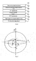
- an embodiment of the invention provides a LCD screen comprising a TFT substrate 601, a CF substrate 602, liquid crystal layer 603 disposed between the TFT substrate 601 and the CF substrate 602, a first polarizing layer 604 at outer side of the TFT substrate, and a second polarizing layer 605 at outer side of the CF substrate 602.
- the LCD screen further comprises:
- the first optical compensation film 606 with its slow axis perpendicular or parallel to the transmission axis of the first polarizing layer 604 is disposed between the first polarizing layer 604 and the TFT substrate 601, in order that a polarized light obtained from a light non-normally incident into the first polarizing layer 604 is changed into a first elliptically polarized light by means of such first optical compensation film 606, wherein the polarization direction of the first elliptically polarized light is the same as that of a polarized light obtained from a light incident into the first polarizing layer 604 at an azimuth angle of 90 degree.
- the liquid crystal layer 603 will not change the polarization direction of the first elliptically polarized light. Also, by means of the phase retardation function of the liquid crystal layer 603, the first elliptically polarized light is converted into a second elliptically polarized light with its polarization direction consistent with that of the first elliptically polarized light and its rotation direction opposite to that of the first elliptically polarized light.
- the transmission axis of the first polarizing layer 604 is parallel to the absorption axis of the second polarizing layer 605, when the light is non-perpendicularly incident into the first polarizing layer 604 and the second polarizing layer 605, the transmission axis of the first polarizing layer 604 deflects in an opposite direction and by an identical magnitude with respect to the deflection of the absorption axis of the second polarizing layer 605. Accordingly, by the second optical compensation film 607 which has a refractivity and a phase retardation as the same as those of the first optical compensation film 606 respectively, the second elliptically polarized light can be compensated into a polarized light capable of being absorbed completely by the second polarizing layer 605. As a result, the optical compensation for the light leakage is achieved.
- the polarization direction of the polarized light obtained from a light incident into the first polarizing layer 604 at a polar angle of 0 degree is identical to that of the polarized light obtained from a light incident into the first polarizing layer 604 at an azimuth angle of 90 degree, thereby the first optical compensation film 606 will not compensate the polarized light.
- the polarized light obtained from a light incident into the first polarizing layer 604 at a polar angle of 0 degree does not deflect, the light leakage will not occur, and thus it is not necessary to compensate.
- the first optical compensation film may be designed for such polarized light so that the best compensation effect can be achieved.
- the foregoing configurations for the first optical compensation film 606, the second optical compensation film 607 and the liquid crystal layer 603 can work in the compensation for the light leakage in any of the O-mode, the E-mode, and the multi domain-mode (which is a mixed mode formed by the O-mode and the E-mode) LCD screens.
- the direction of the slow axis of the liquid crystal layer 603 may consist with the transmission axis of the first polarizing layer, or the direction of the slow axis of the liquid crystal molecules in the liquid crystal layer 603 may consist with the transmission axis of the second polarizing layer; or the liquid crystal molecules are mixed liquid crystal molecules formed by a type of liquid crystal molecules with its direction of slow axis consistent with the transmission axis of the first polarizing layer and a type of liquid crystal molecules with its direction of slow axis consistent with the transmission axis of the second polarizing layer. That is to say, the liquid crystal layer 603 may be formed by the O-mode liquid crystal material, the E-mode liquid crystal material, or the multi domain-mode liquid crystal material which is formed by the O-mode and the E-mode liquid crystal materials.
- the refractivities and the phase retardants of the first optical compensation film 606 and the second optical compensation film 607 and the phase retardant of the liquid crystal layer 603 may be set so that the first optical compensation film 606 can compensate the polarized light obtained from a light non-perpendicularly incident into the first polarizing layer 604 to obtain the first elliptically polarized light, and that the liquid crystal layer 603 can convert the first elliptically polarized light into the second elliptically polarized light with its polarization direction consistent with that of the first elliptically polarized light and its rotation direction opposite to that of the first elliptically polarized light.
- the refractivities and the phase retardants of the first optical compensation film 606 and the second optical compensation film 607 and the phase retardant of the liquid crystal layer 603 may be determined based on empiric values, as long as such first optical compensation film 606 can compensate the polarized light obtained from a light non-perpendicularly incident into the first polarizing layer 604 to obtain the first elliptically polarized light, and such liquid crystal layer 603 can convert the first elliptically polarized light into the second elliptically polarized light with its polarization direction consistent with that of the first elliptically polarized light and its rotation direction opposite to that of the first elliptically polarized light.
- the slow axis of the first optical compensation film 606 when the slow axis of the first optical compensation film 606 is parallel to the transmission axis of the first polarizing layer 604, it may be configured that the refractivity of the first optical compensation film 606 is larger or equal to 0.25, the phase retardant of the first optical compensation film 606 is 20 nm to 280 nm, and the phase retardant of the liquid crystal layer 603 is 270 nm to 560 nm.
- the point T represents the polarization direction of a polarized light obtained from a light incident into the first polarizing layer 604 at an azimuth angle of 45 degree
- the point A represents the polarization direction corresponding to the absorption axis of the second polarizing layer 605 when a light is incident into the first polarizing layer 604 at an azimuth angle of 45 degree
- the point O represents the polarization direction of a polarized light obtained from a light incident into the first polarizing layer 604 at an azimuth angle of 90 degree.
- the distance on the equator between the points A and O (hereinafter referred as "AO" in brief) and the distance on the equator between the points O and T (hereinafter referred as "OT” in brief) are identical to each other.
- AO polarized light with its polarization state corresponding to the point T transmits through the first optical compensation film 606, its polarization state deflects to the point B.
- the point B represents an elliptically polarized light with a polarization direction consistent with the polarization direction at the point O.
- the polarized light with its polarization state corresponding to the point B transmits through the E-mode liquid crystal layer 603, its polarization state varies to the point C.
- the variation trace of its polarization state is shown as the arc BC.
- the point C represents an elliptically polarized light with a polarization direction identical to and a rotation direction opposite to those at the point B.
- the polarized light corresponding to the point C transmits through the second optical compensation film 607, its polarization state varies to the point A.
- this polarized light can be absorbed completely so that the light leakage will not occur.
- the point T represents the polarization direction of a polarized light obtained from a light incident into the first polarizing layer 604 at an azimuth angle of 45 degree
- the point A represents the polarization direction corresponding to the absorption axis of the second polarizing layer 605 when a light is non-perpendicularly incident into the first polarizing layer 604
- the point O represents the polarization direction of a polarized light obtained from a light incident into the first polarizing layer 604 at an azimuth angle of 90 degree.
- the distances AO and OT both of which are on the equator, are identical to each other.
- a polarized light with its polarization state corresponding to the point T transmits through the first optical compensation film 606, its polarization state deflects to the point B.
- the point B represents an elliptically polarized light with a polarization direction consistent with the polarization direction at the point O.
- the polarized light with its polarization state being at the point B transmits through the E-mode liquid crystal layer 603, its polarization state varies to the point C.
- the variation trace of its polarization state is shown as the arc BC.
- the point C represents an elliptically polarized light with a polarization direction identical to and a rotation direction opposite to those at the point B.
- the phase retardant of the first optical compensation film 606 may be set smaller and the phase retardant of the liquid crystal layer 603 may be set smaller, so that a better compensation effect may be achieved.
- the phase retardant of the first optical compensation film 606 may be set to 270 nm to 280 nm, and the phase retardant of the liquid crystal layer 603 may be set to 540 nm to 560 nm.
- the phase retardant of the first optical compensation film 606 may be set to 80 nm to 110 nm, and the phase retardant of the liquid crystal layer 603 may be set to 340 nm to 370 nm.
- the phase retardant of the first optical compensation film 606 may be set to 35 nm to 60 nm, and the phase retardant of the liquid crystal layer 603 may be set to 280 nm to 320 nm.
- any other feasible settings for the reflectivity and the phase retardant of the first optical compensation film 606 and the phase retardant of the liquid crystal layer 603 may be conceivable by a skilled in the art, and will not be repeated herein.
- the slow axis of the first optical compensation film 606 when the slow axis of the first optical compensation film 606 is perpendicular to the transmission axis of the first polarizing layer 604, it may be configured that the refractivity of the first optical compensation film 606 is smaller or equal to 0.25, the phase retardant of the first optical compensation film 606 is 20 nm to 280 nm, and the phase retardant of the liquid crystal layer is 270 nm to 560 nm.
- the point T represents the polarization direction of a polarized light obtained from a light incident into the first polarizing layer 604 at an azimuth angle of 45 degree
- the point A represents the polarization direction corresponding to the absorption axis of the second polarizing layer 605 when a light is incident into the first polarizing layer 604 at an azimuth angle of 45 degree
- the point O represents the polarization direction of a polarized light obtained from a light incident into the first polarizing layer 604 at an azimuth angle of 90 degree.
- the distances AO and OT both of which are on the equator, are identical to each other.
- the point B represents an elliptically polarized light with a polarization direction consistent with the polarization direction at the point O.
- the polarized light with its polarization state corresponding to the point B transmits through the E-mode liquid crystal layer 603
- its polarization state varies to the point C
- the variation trace of its polarization state is shown as the arc BC.
- the point C represents an elliptically polarized light with a polarization direction identical to and a rotation direction opposite to those at the point B.
- the polarized light corresponding to the point C transmits through the second optical compensation film 607, its polarization state varies to the point A.
- this polarized light can be absorbed completely so that the light leakage will not occur.
- the point T represents the polarization direction of a polarized light obtained from a light non-perpendicularly incident into the first polarizing layer 604
- the point A represents the polarization direction corresponding to the absorption axis of the second polarizing layer 605 when a light is incident into the first polarizing layer 604 at an azimuth angle of 45 degree
- the point O represents the polarization direction of a polarized light obtained from a light incident into the first polarizing layer 604 at an azimuth angle of 90 degree.
- the distances AO and OT both of which are on the equator, are identical to each other.
- the point B represents an elliptically polarized light with a polarization direction consistent with the polarization direction at the point O.
- the polarized light with its polarization state corresponding to the point B transmits through the E-mode liquid crystal layer 603
- its polarization state varies to the point C
- the variation trace of its polarization state is shown as the arc BC.
- the point C represents an elliptically polarized light with a polarization direction identical to and a rotation direction opposite to those at the point B.
- the polarized light corresponding to the point C transmits through the second optical compensation film 607, its polarization state varies to the point A.
- this polarized light can be absorbed completely so that the light leakage will not occur.
- the phase retardant of the first optical compensation film 606 may be set smaller and the phase retardant of the liquid crystal layer 603 may be set smaller, so that a better compensation effect may be achieved.
- the phase retardant of the first optical compensation film 606 may be set to 80 nm to 110 nm, and the phase retardant of the liquid crystal layer 603 may be set to 340 nm to 370 nm.
- the phase retardant of the first optical compensation film 606 may be set to 35 nm to 60 nm, and the phase retardant of the liquid crystal layer 603 may be set to 280 nm to 320 nm.
- any other feasible settings for the reflectivity and the phase retardant of the first optical compensation film 606 and the phase retardant of the liquid crystal layer 603 may be conceivable by a skilled in the art, and will not be repeated herein.
- An embodiment of the invention further provides a display device which comprises any one of the above mentioned LCD screens.
- Such display device may be any product or component with display function, such as liquid crystal panel, electronic paper, OLED panel, mobile telephone, tablet PC, television, display, laptop, digital album, navigator, and so on.
Landscapes
- Physics & Mathematics (AREA)
- Nonlinear Science (AREA)
- Mathematical Physics (AREA)
- Chemical & Material Sciences (AREA)
- Crystallography & Structural Chemistry (AREA)
- General Physics & Mathematics (AREA)
- Optics & Photonics (AREA)
- Polarising Elements (AREA)
- Liquid Crystal (AREA)
Abstract

Description
- The present invention relates to liquid crystal display technology, and in particular, to a liquid crystal display screen and a display device.
- The In-Plane Switching (IPS) technology is a wide-viewing angle technology applied to liquid crystal display (LCD), which is widely used in manufacturing LCD television to improve the viewing angle effectively. As shown in
Fig. 1 , an electrode structure of such LCD television includesfirst electrodes 101 andsecond electrodes 102, and the liquid crystal molecules in the IPS-mode display are arranged in parallel with each other when no voltage is applied to the electrode structure. - The Advanced Super Dimension Switch (ADS) technology is a core technology of planar-electric-field wide-viewing angle, in which a multidimensional electric field is formed by an electric field generated from the edges of the slit electrodes located in a same plane and an electric field generated between the slit electrode layer and the plate electrode layer, so that all the liquid crystal molecules located among the slit electrodes and located right over the slit electrodes in the liquid crystal cell can rotate. Thus, both the operating efficiency and the transmission efficiency of the liquid crystal material are improved. With the ADS technology, the TFT-LCD product has the advantages of improved picture quality, high resolution, high transmittance, low power consumption, wide viewing angle, high aperture ratio, low chromatic aberration, no squeezing water ripples, etc.. For different applications, the improved ADS technologies include high-transmittance I-ADS technology, high-aperture ratio H-ADS technology and high-resolution S-ADS technology, and so on. As shown in
Fig. 2 , the electrode structure of ADS-mode LCD screen comprises a color filter (CF)substrate 201, array substrate including a plural of thin film transistors (TFTs) (hereinafter referred as thin film transistor substrate or TFT substrate) 205 disposed opposite to theCF substrate 201, and afirst electrode 204, aninsulating layer 203 andsecond electrodes 202, which are disposed between theCF substrate 201 and theTFT substrate 205 in this order, from bottom to top. Similar to that in the IPS-mode LCD screen, the liquid crystal molecules in the ADS-mode LCD screen are also arranged in parallel with each other when no voltage is applied to the electrode structure. - In order to enable the LCD screen to forming images, it is necessary to provide a polarizing layer to the upper side and the lower side of the liquid crystal cell (including the TFT substrate and the CF substrate opposite to each other, and the liquid crystal layer between the TFT substrate and the CF substrate), respectively, that is, a first polarizing layer located at the TFT substrate side and a second polarizing layer located at the CF substrate side. In both the IPS-mode and the ADS-mode LCD screens, the transmission axis of the first polarizing layer is perpendicular to the transmission axis of the second polarizing layer, and parallel to the absorption axis of the second polarizing layer. When not being applied with power, the polarized light transmitting through the first polarizing layer is absorbed by the second polarizing layer completely. However, light leakage may occur in both the IPS-mode and the ADS-mode LCD screens. For example, in the case that the azimuth angle of the incident light with respect to the polarizing layer is 45°, and the polar angle of the incident light with respect to the polarizing layer is 60°, the light leakage is most severe. The principle of the light leakage will be described with reference to
Fig. 3 . The light leakage results from that, when the light transmits along above directions, the transmission axes of the polarizing layers at the upper and the lower sides of the liquid crystal cell are not orthogonal to each other, and the direction of the light axis of the liquid crystal molecules is changed to some extent. - In the following description, such change will be described by using the Poincare Sphere. The Poincare Sphere is a mathematic model invented by the Jules Henri Poincaré in 1892. In the stokes space, it is introduced the normalized radius S0=1; S02=S12+S22+S32, wherein S1, S2 and S3 correspond to the coordinates x, y and z of the solid sphere respectively, and are used to represent the polarization state of the light. Any one point on the sphere corresponds to a certain polarization state of the completely polarized light with unit intensity. The points at the equator of the Poincare Sphere represent linearly polarized light, the upper and lower poles correspond to right-circularly polarized light and left-circularly polarized light respectively, and other points correspond to elliptically polarized light. The polarized lights corresponding to the points at the same longitude on the Poincare Sphere have identical polarized directions.
- As shown in
Fig. 3 , when the incident light is incident into the first polarizing layer at a polar angle of 60 degree and an azimuth angle of 45 degree, the transmission axis of the first polarizing layer on the TFT substrate side will deflect to the point T in the figure, while the absorption axis of the second polarizing layer on the CF substrate side will deflect to the point A in the figure. Since the transmission axis of the first polarizing layer and the absorption axis of the second polarizing layer do not consist with each other any more, and the light axis of the liquid crystal molecules also deflect by a certain angle at the same time, the polarized light transmitting through the first polarizing layer cannot be absorbed by the second polarizing layer completely, and thus the light leakage occurs. - Nowadays, the wide-viewing angle optical compensation for the ADS-mode and IPS-mode LCD screens has been widely applicable. However, the existing optical compensation methods each only works for a certain display mode of the LCD screen. The display modes of the ADS-mode and IPS-mode LCD screens may be classified into an E mode, an O mode and a multi domain mode. In an E-mode LCD screen, the direction of the slow axis of the liquid crystal molecules consists with the direction of the transmission axis of the first polarizing layer on the TFT substrate side. In an O-mode LCD screen, the direction of the slow axis of the liquid crystal molecules consists with the direction of the transmission axis of the second polarizing layer on the CF substrate side. The multi domain mode is a mixed mode formed by the E mode and the O mode. For an E-mode LCD screen, the compensation film should be disposed between the TFT substrate and the first polarizing layer on the TFT substrate side. For an O-mode LCD screen, the compensation film should be disposed between the CF substrate and the second polarizing layer on the CF substrate side. For the multi domain mode, there is still no any proper optical compensation method nowadays. The reasons are presented as follows.
- In the E-mode liquid crystal display screen, the transmission axis of the first polarizing layer and the slow axis of the liquid crystal molecule will deflect to the point A shown in
Fig. 3 since the slow axis of the liquid crystal molecule consists with the transmission axis of the first polarizing layer in direction. In this case, the compensation may be achieved only by performing compensation such that the polarization direction of the polarized light incident from the TFT substrate side is changed from the point T to the point A before the polarized light incident from the TFT substrate side transmits through the liquid crystal material. The liquid crystal material without being applied with voltage will not change the polarization direction of the polarized light, which enables the polarized light having transmitted through the liquid crystal material to be directly absorbed by the second polarizing layer on the CF substrate side. The optical-compensated structure for the E-mode liquid crystal display screen is shown inFig. 4 . - In the E-mode liquid crystal display screen, the optical axis of the liquid crystal molecule will deflect to the point T shown in
Fig. 3 . The polarization direction of the polarized light incident from the TFT substrate side still directs to the point T after the polarized light incident from the TFT substrate side transmits through the liquid crystal material. The liquid crystal material without being applied with voltage will not change the polarization direction of the polarized light. Accordingly, if the polarization direction of the polarized light is compensated to change from the point T to the point A after the polarized light transmits through the liquid crystal material, it can ensure that the light incident to the second polarizing layer may be completely absorbed. The optical-compensated structure for the O-mode liquid crystal display screen is shown inFig. 5 . - The multi domain-mode liquid crystals of IPS mode and ADS mode liquid crystal display screens may be classified into two types. In one type of the liquid crystal, the liquid crystal molecules have two initial orientations perpendicular to each other, and may be obtained by way of the optical orientation. In the other type of the liquid crystal, the liquid crystal molecules have a unique initial orientation and may be obtained by ways of the ordinary film orientation and the optical orientation, in which there is a certain angle between the electrodes. Despite of the type of the multi domain-mode liquid crystal, a method for optically compensating the light leakage has not been proposed for the LCD with multi domain-mode liquid crystal since it is a mixture mode of E- and O- modes.
- In general, the methods for optically compensating the light leakage are different between the LCD of E-mode and that of O-mode at present. Furthermore, it has not been proposed an optical compensation method for the LCD with multi domain-mode liquid crystal formed by E-mode and O-mode liquid crystal.
- The embodiments of the invention provide a LCD screen and a display device which can achieve compensation for the light leakage occurring in any of the LCD screens of E mode, of O mode and of multi-domain mode formed by E mode and O mode.
- A liquid crystal display (LCD) screen comprises a thin film transistor (TFT) substrate, a color filter (CF) substrate, liquid crystal layer disposed between the TFT substrate and the CF substrate, a first polarizing layer at outer side of the TFT substrate, and a second polarizing layer at outer side of the CF substrate, wherein it further comprises:
- a first optical compensation film disposed between the first polarizing layer and the TFT substrate, a slow axis of which is parallel or perpendicular to a transmission axis of the first polarizing layer, the first optical compensation film being configured to compensate a polarized light obtained from a light non-normally incident into the first polarizing layer so that the polarized light becomes a first elliptically polarized light, polarization direction of the first elliptically polarized light is the same as that of a polarized light obtained from a light incident into the first polarizing layer at an azimuth angle of 90 degree;
- a second optical compensation film disposed between the second polarizing layer and the CF substrate, a slow axis of which is perpendicular to the slow axis of the first optical compensation film, a refractivity and a phase retardation of the second optical compensation film are the same as those of the first optical compensation respectively, and
- the liquid crystal layer configured to convert the first elliptically polarized light into a second elliptically polarized light, with its polarization direction consistent with that of the first elliptically polarized light and its rotation direction opposite to that of the first elliptically polarized light.
- A display device comprises a LCD screen provided by any one of the embodiment of the invention.
- The embodiments of the invention provide a LCD screen and a display device which utilize the characteristics that the liquid crystal material will not change the polarization direction of the polarized light obtained from a light incident into the first polarizing layer at an azimuth angle of 90 degree, and that the transmission axis of the first polarizing layer and the absorption axis of the second polarizing layer will deflect in opposite directions and by identical magnitude if the light is incident into the first polarizing layer. Based on such characteristics, a first and a second optical compensation films are disposed on each side of the liquid crystal layer, respectively. A polarized light obtained from a light non-normally incident into a first polarizing layer is compensated by means of the first optical compensation film so that the polarized light becomes a first elliptically polarized light. Also, by means of the phase retardation function of the liquid crystal, the first elliptically polarized light is converted into a second elliptically polarized light with its polarization direction consistent with that of the first elliptically polarized light and its rotation direction opposite to that of the first elliptically polarized light. Then, by means of the second optical compensation film, the second elliptically polarized light is compensated into a polarized light capable of being absorbed completely by a second polarizing layer. Thus, compensation for the light leakage occurring in any of the LCD screens of E mode, of O mode and of multi domain mode formed by E mode and O mode is achieved.
-
-
Fig. 1 shows an electrode structure of the IPS-mode LCD screen according to the prior art; -
Fig. 2 shows an electrode structure of the ADS-mode LCD screen according to the prior art; -
Fig. 3 is a schematic diagram illustrating the deflection of the transmission axis of the first polarizing layer and the deflection of the absorption axis of the second polarizing layer when the incident light is incident into the first polarizing layer at a polar angle of 60 degree and a azimuth angle of 45 degree, according to the prior art; -
Fig. 4 is a schematic diagram illustrating a structure of E-mode LCD screen according to the prior art; -
Fig. 5 is a schematic diagram illustrating a structure of O-mode LCD screen according to the prior art; -
Fig. 6 is a schematic diagram illustrating a structure of a LCD screen according to an embodiment of the invention; -
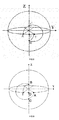
Fig. 7 is a schematic diagram illustrating a Poincare Sphere for optically compensating an E-mode LCD screen according to an embodiment of the invention; -
Fig. 8 is a schematic diagram illustrating a Poincare Sphere for optically compensating an O-mode LCD screen according to an embodiment of the invention; -
Fig. 9 is another schematic diagram illustrating a Poincare Sphere for optically compensating an E-mode LCD screen according to an embodiment of the invention; and -
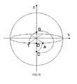
Fig. 10 is another schematic diagram illustrating a Poincare Sphere for optically compensating an O-mode LCD screen according to an embodiment of the invention. - As shown in
Fig. 6 , an embodiment of the invention provides a LCD screen comprising aTFT substrate 601, aCF substrate 602,liquid crystal layer 603 disposed between theTFT substrate 601 and theCF substrate 602, a firstpolarizing layer 604 at outer side of the TFT substrate, and a secondpolarizing layer 605 at outer side of theCF substrate 602. The LCD screen further comprises: - a first optical compensation film 606 disposed between the first
polarizing layer 604 and theTFT substrate 601, a slow axis of which is parallel or perpendicular to a transmission axis of the firstpolarizing layer 604, the first optical compensation film 606 being configured to compensate a polarized light obtained from a light non-normally incident into the firstpolarizing layer 604 so that the polarized light becomes a first elliptically polarized light, polarization direction of the first elliptically polarized light is the same as that of a polarized light obtained from a light incident at an azimuth angle of 90 degree into the firstpolarizing layer 604; - a second
optical compensation film 607 disposed between the secondpolarizing layer 605 and theCF substrate 602, a slow axis of which is perpendicular to the slow axis of the first optical compensation film 606, a refractivity and a phase retardation of the secondoptical compensation film 607 are the same as those of the first optical compensation 606 respectively; and - the
liquid crystal layer 603, which is configured to convert the first elliptically polarized light into a second elliptically polarized light, with its polarization direction consistent with that of the first elliptically polarized light and its rotation direction opposite to that of the first elliptically polarized light. - Since the
liquid crystal layer 603 without being applied with voltage will not change the polarization direction of the polarized light obtained from a light incident into the firstpolarizing layer 604 at an azimuth angle of 90 degree, the first optical compensation film 606 with its slow axis perpendicular or parallel to the transmission axis of the firstpolarizing layer 604 is disposed between the firstpolarizing layer 604 and theTFT substrate 601, in order that a polarized light obtained from a light non-normally incident into the firstpolarizing layer 604 is changed into a first elliptically polarized light by means of such first optical compensation film 606, wherein the polarization direction of the first elliptically polarized light is the same as that of a polarized light obtained from a light incident into the firstpolarizing layer 604 at an azimuth angle of 90 degree. In this case, theliquid crystal layer 603 will not change the polarization direction of the first elliptically polarized light. Also, by means of the phase retardation function of theliquid crystal layer 603, the first elliptically polarized light is converted into a second elliptically polarized light with its polarization direction consistent with that of the first elliptically polarized light and its rotation direction opposite to that of the first elliptically polarized light. Furthermore, since the transmission axis of the firstpolarizing layer 604 is parallel to the absorption axis of the secondpolarizing layer 605, when the light is non-perpendicularly incident into the firstpolarizing layer 604 and the secondpolarizing layer 605, the transmission axis of the firstpolarizing layer 604 deflects in an opposite direction and by an identical magnitude with respect to the deflection of the absorption axis of the secondpolarizing layer 605. Accordingly, by the secondoptical compensation film 607 which has a refractivity and a phase retardation as the same as those of the first optical compensation film 606 respectively, the second elliptically polarized light can be compensated into a polarized light capable of being absorbed completely by the secondpolarizing layer 605. As a result, the optical compensation for the light leakage is achieved. - The polarization direction of the polarized light obtained from a light incident into the first
polarizing layer 604 at a polar angle of 0 degree is identical to that of the polarized light obtained from a light incident into the firstpolarizing layer 604 at an azimuth angle of 90 degree, thereby the first optical compensation film 606 will not compensate the polarized light. In addition, since the polarized light obtained from a light incident into the firstpolarizing layer 604 at a polar angle of 0 degree does not deflect, the light leakage will not occur, and thus it is not necessary to compensate. As a result, in the LCD screen according to the embodiment of the invention, the light leakage will be overcome by the optical compensation for the polarized light obtained from a light non-perpendicularly incident into the firstpolarized layer 604. Particularly, since the serious deflection of the polarized light obtained from a light incident into the firstpolarizing layer 604 at a polar angle of 60 degree and an azimuth angle of 45 degree, the first optical compensation film may be designed for such polarized light so that the best compensation effect can be achieved. - The foregoing configurations for the first optical compensation film 606, the second
optical compensation film 607 and theliquid crystal layer 603 can work in the compensation for the light leakage in any of the O-mode, the E-mode, and the multi domain-mode (which is a mixed mode formed by the O-mode and the E-mode) LCD screens. Thus, in the LCD screen according to the invention, the direction of the slow axis of theliquid crystal layer 603 may consist with the transmission axis of the first polarizing layer, or the direction of the slow axis of the liquid crystal molecules in theliquid crystal layer 603 may consist with the transmission axis of the second polarizing layer; or the liquid crystal molecules are mixed liquid crystal molecules formed by a type of liquid crystal molecules with its direction of slow axis consistent with the transmission axis of the first polarizing layer and a type of liquid crystal molecules with its direction of slow axis consistent with the transmission axis of the second polarizing layer. That is to say, theliquid crystal layer 603 may be formed by the O-mode liquid crystal material, the E-mode liquid crystal material, or the multi domain-mode liquid crystal material which is formed by the O-mode and the E-mode liquid crystal materials. - Further, the refractivities and the phase retardants of the first optical compensation film 606 and the second
optical compensation film 607 and the phase retardant of theliquid crystal layer 603 may be set so that the first optical compensation film 606 can compensate the polarized light obtained from a light non-perpendicularly incident into the firstpolarizing layer 604 to obtain the first elliptically polarized light, and that theliquid crystal layer 603 can convert the first elliptically polarized light into the second elliptically polarized light with its polarization direction consistent with that of the first elliptically polarized light and its rotation direction opposite to that of the first elliptically polarized light. - In practice, the refractivities and the phase retardants of the first optical compensation film 606 and the second
optical compensation film 607 and the phase retardant of theliquid crystal layer 603 may be determined based on empiric values, as long as such first optical compensation film 606 can compensate the polarized light obtained from a light non-perpendicularly incident into the firstpolarizing layer 604 to obtain the first elliptically polarized light, and suchliquid crystal layer 603 can convert the first elliptically polarized light into the second elliptically polarized light with its polarization direction consistent with that of the first elliptically polarized light and its rotation direction opposite to that of the first elliptically polarized light. - For example, when the slow axis of the first optical compensation film 606 is parallel to the transmission axis of the first
polarizing layer 604, it may be configured that the refractivity of the first optical compensation film 606 is larger or equal to 0.25, the phase retardant of the first optical compensation film 606 is 20 nm to 280 nm, and the phase retardant of theliquid crystal layer 603 is 270 nm to 560 nm. - Next, the effect of such configurations on the light leakage of the E-mode and the O-mode liquid crystal molecules will be analyzed by using the Poincare sphere.
- For the
liquid crystal layer 603 in E-mode LCD screen, as shown inFig. 7 , the point T represents the polarization direction of a polarized light obtained from a light incident into the firstpolarizing layer 604 at an azimuth angle of 45 degree, the point A represents the polarization direction corresponding to the absorption axis of the secondpolarizing layer 605 when a light is incident into the firstpolarizing layer 604 at an azimuth angle of 45 degree, and the point O represents the polarization direction of a polarized light obtained from a light incident into the firstpolarizing layer 604 at an azimuth angle of 90 degree. The distance on the equator between the points A and O (hereinafter referred as "AO" in brief) and the distance on the equator between the points O and T (hereinafter referred as "OT" in brief) are identical to each other. After a polarized light with its polarization state corresponding to the point T transmits through the first optical compensation film 606, its polarization state deflects to the point B. The point B represents an elliptically polarized light with a polarization direction consistent with the polarization direction at the point O. When the polarized light with its polarization state corresponding to the point B transmits through the E-modeliquid crystal layer 603, its polarization state varies to the point C. The variation trace of its polarization state is shown as the arc BC. The point C represents an elliptically polarized light with a polarization direction identical to and a rotation direction opposite to those at the point B. After the polarized light corresponding to the point C transmits through the secondoptical compensation film 607, its polarization state varies to the point A. Thus, this polarized light can be absorbed completely so that the light leakage will not occur. - For the
liquid crystal layer 603 in O-mode LCD screen, as shown inFig. 8 , the point T represents the polarization direction of a polarized light obtained from a light incident into the firstpolarizing layer 604 at an azimuth angle of 45 degree, the point A represents the polarization direction corresponding to the absorption axis of the secondpolarizing layer 605 when a light is non-perpendicularly incident into the firstpolarizing layer 604, and the point O represents the polarization direction of a polarized light obtained from a light incident into the firstpolarizing layer 604 at an azimuth angle of 90 degree. The distances AO and OT, both of which are on the equator, are identical to each other. After a polarized light with its polarization state corresponding to the point T transmits through the first optical compensation film 606, its polarization state deflects to the point B. The point B represents an elliptically polarized light with a polarization direction consistent with the polarization direction at the point O. When the polarized light with its polarization state being at the point B transmits through the E-modeliquid crystal layer 603, its polarization state varies to the point C. The variation trace of its polarization state is shown as the arc BC. The point C represents an elliptically polarized light with a polarization direction identical to and a rotation direction opposite to those at the point B. After the polarized light corresponding to the point C transmits through the secondoptical compensation film 607, its polarization state varies to the point A. Thus, this polarized light can be absorbed completely so that the light leakage will not occur. - Specifically, as the reflectivity of the first optical compensation film 606 is set larger, the phase retardant of the first optical compensation film 606 may be set smaller and the phase retardant of the
liquid crystal layer 603 may be set smaller, so that a better compensation effect may be achieved. When the reflectivity of the first optical compensation film 606 is set to 0.25, the phase retardant of the first optical compensation film 606 may be set to 270 nm to 280 nm, and the phase retardant of theliquid crystal layer 603 may be set to 540 nm to 560 nm. When the reflectivity of the first optical compensation film 606 is set to 1, the phase retardant of the first optical compensation film 606 may be set to 80 nm to 110 nm, and the phase retardant of theliquid crystal layer 603 may be set to 340 nm to 370 nm. When the reflectivity of the first optical compensation film 606 is set to 3.5, the phase retardant of the first optical compensation film 606 may be set to 35 nm to 60 nm, and the phase retardant of theliquid crystal layer 603 may be set to 280 nm to 320 nm. - Of course, in the case that the slow axis of the first optical compensation film 606 is parallel to the transmission axis of the first
polarizing layer 604, any other feasible settings for the reflectivity and the phase retardant of the first optical compensation film 606 and the phase retardant of theliquid crystal layer 603 may be conceivable by a skilled in the art, and will not be repeated herein. - For example, when the slow axis of the first optical compensation film 606 is perpendicular to the transmission axis of the first
polarizing layer 604, it may be configured that the refractivity of the first optical compensation film 606 is smaller or equal to 0.25, the phase retardant of the first optical compensation film 606 is 20 nm to 280 nm, and the phase retardant of the liquid crystal layer is 270 nm to 560 nm. - Next, the effect of such configurations on the light leakage of the E-mode and the O-mode LCD screens will be analyzed by using the Poincare sphere.
- For the
liquid crystal layer 603 in E-mode LCD screen, as shown inFig. 9 , the point T represents the polarization direction of a polarized light obtained from a light incident into the firstpolarizing layer 604 at an azimuth angle of 45 degree, the point A represents the polarization direction corresponding to the absorption axis of the secondpolarizing layer 605 when a light is incident into the firstpolarizing layer 604 at an azimuth angle of 45 degree, and the point O represents the polarization direction of a polarized light obtained from a light incident into the firstpolarizing layer 604 at an azimuth angle of 90 degree. The distances AO and OT, both of which are on the equator, are identical to each other. After a polarized light with its polarization state corresponding to the point T transmits through the first optical compensation film 606, its polarization state deflects to the point B. The point B represents an elliptically polarized light with a polarization direction consistent with the polarization direction at the point O. When the polarized light with its polarization state corresponding to the point B transmits through the E-modeliquid crystal layer 603, its polarization state varies to the point C, and the variation trace of its polarization state is shown as the arc BC. The point C represents an elliptically polarized light with a polarization direction identical to and a rotation direction opposite to those at the point B. After the polarized light corresponding to the point C transmits through the secondoptical compensation film 607, its polarization state varies to the point A. Thus, this polarized light can be absorbed completely so that the light leakage will not occur. - For the
liquid crystal layer 603 in O-mode LCD screen, as shown inFig. 10 , the point T represents the polarization direction of a polarized light obtained from a light non-perpendicularly incident into the firstpolarizing layer 604, the point A represents the polarization direction corresponding to the absorption axis of the secondpolarizing layer 605 when a light is incident into the firstpolarizing layer 604 at an azimuth angle of 45 degree, and the point O represents the polarization direction of a polarized light obtained from a light incident into the firstpolarizing layer 604 at an azimuth angle of 90 degree. The distances AO and OT, both of which are on the equator, are identical to each other. After a polarized light with its polarization state corresponding to the point T transmits through the first optical compensation film 606, its polarization state deflects to the point B. The point B represents an elliptically polarized light with a polarization direction consistent with the polarization direction at the point O. When the polarized light with its polarization state corresponding to the point B transmits through the E-modeliquid crystal layer 603, its polarization state varies to the point C, and the variation trace of its polarization state is shown as the arc BC. The point C represents an elliptically polarized light with a polarization direction identical to and a rotation direction opposite to those at the point B. After the polarized light corresponding to the point C transmits through the secondoptical compensation film 607, its polarization state varies to the point A. Thus, this polarized light can be absorbed completely so that the light leakage will not occur. - Specifically, as the reflectivity of the first optical compensation film 606 is set smaller, the phase retardant of the first optical compensation film 606 may be set smaller and the phase retardant of the
liquid crystal layer 603 may be set smaller, so that a better compensation effect may be achieved. When the reflectivity of the first optical compensation film 606 is set to 0, the phase retardant of the first optical compensation film 606 may be set to 80 nm to 110 nm, and the phase retardant of theliquid crystal layer 603 may be set to 340 nm to 370 nm. When the reflectivity of the first optical compensation film 606 is set to -2.85, the phase retardant of the first optical compensation film 606 may be set to 35 nm to 60 nm, and the phase retardant of theliquid crystal layer 603 may be set to 280 nm to 320 nm. - Of course, in the case that the slow axis of the first optical compensation film 606 is perpendicular to the transmission axis of the first
polarizing layer 604, any other feasible settings for the reflectivity and the phase retardant of the first optical compensation film 606 and the phase retardant of theliquid crystal layer 603 may be conceivable by a skilled in the art, and will not be repeated herein. - An embodiment of the invention further provides a display device which comprises any one of the above mentioned LCD screens. Such display device may be any product or component with display function, such as liquid crystal panel, electronic paper, OLED panel, mobile telephone, tablet PC, television, display, laptop, digital album, navigator, and so on.
- It is obviously for a skilled in the art that various modifications and variations may be made to the invention without departing from the spirit and scope of the invention. Thus, the invention is intended to cover these modifications and variations provided that they fall into the scope of the attached claims and its equivalent.
Claims (10)
- A liquid crystal display screen, comprising a thin film transistor substrate, a color filter substrate, liquid crystal layer disposed between the thin film transistor substrate and the color filter substrate, a first polarizing layer at outer side of the thin film transistor substrate, and a second polarizing layer at outer side of the color filter substrate, wherein further comprising:a first optical compensation film disposed between the first polarizing layer and the thin film transistor substrate, a slow axis of which is parallel or perpendicular to a transmission axis of the first polarizing layer, the first optical compensation film being configured to compensate a polarized light obtained from a light non-normally incident into the first polarizing layer so that the polarized light becomes a first elliptically polarized light, polarization direction of the first elliptically polarized light is the same as that of a polarized light obtained from a light incident into the first polarizing layer at an azimuth angle of 90 degree;a second optical compensation film disposed between the second polarizing layer and the color filter substrate, a slow axis of which is perpendicular to that of the first optical compensation film, a refractivity and a phase retardation of the second optical compensation film are the same as those of the first optical compensation respectively, andwherein the liquid crystal layer is configured to convert the first elliptically polarized light into a second elliptically polarized light, with its polarization direction consistent with that of the first elliptically polarized light and its rotation direction opposite to that of the first elliptically polarized light.
- The liquid crystal display screen of claim 1, wherein
a direction of a slow axis of liquid crystal molecules in the liquid crystal layer is consistent with the transmission axis of the first polarizing layer; or
the direction of the slow axis of the liquid crystal molecules is consistent with a transmission axis of the second polarizing layer; or
the liquid crystal molecules is a mixed liquid crystal molecules formed by a type of liquid crystal molecules with a direction of slow axis consistent with the transmission axis of the first polarizing layer and a type of liquid crystal molecules with a direction of slow axis consistent with the transmission axis of the second polarizing layer. - The liquid crystal display screen of claim 1 or 2, wherein
when the slow axis of the first optical compensation film is parallel to the transmission axis of the first polarizing layer, the reflectivity of the first optical compensation film is larger than or equal to 0.25, the phase retardation of the first optical compensation film is 20 nm - 280 nm, and a phase retardation of the liquid crystal layer is 270 nm - 560 nm. - The liquid crystal display screen of any of the claims 1 to 3, wherein
the reflectivity of the first optical compensation film is 0.25, the phase retardation of the first optical compensation film is 270 nm - 280 nm, and the phase retardation of the liquid crystal layer is 540 nm - 560 nm. - The liquid crystal display screen of of any of the claims 1 to 4, wherein
the reflectivity of the first optical compensation film is 1, the phase retardation of the first optical compensation film is 80 nm - 110 nm, and the phase retardation of the liquid crystal layer is 340 nm - 370 nm. - The liquid crystal display screen of of any of the claims 1 to 5, wherein
the reflectivity of the first optical compensation film is 3.5, the phase retardation of the first optical compensation film is 35 nm - 60 nm, and the phase retardation of the liquid crystal layer is 280 nm - 320 nm. - The liquid crystal display screen of any of the claims 1 to 6, wherein
when the slow axis of the first optical compensation film is perpendicular to the transmission axis of the first polarizing layer, the reflectivity of the first optical compensation film is smaller than or equal to 0.25, the phase retardation of the first optical compensation film is 20 nm - 280 nm, and a phase retardation of the liquid crystal layer is 270 nm - 560 nm. - The liquid crystal display screen of any of the claims 1 to 7, wherein
the reflectivity of the first optical compensation film is 0, the phase retardation of the first optical compensation film is 80 nm - 110 nm, and the phase retardation of the liquid crystal layer is 340 nm - 370 nm. - The liquid crystal display screen of any of the claims 1 to 8, wherein
the reflectivity of the first optical compensation film is -2.85, the phase retardation of the first optical compensation film is 35 nm - 60 nm, and the phase retardation of the liquid crystal layer is 280 nm - 320 nm. - A display device, comprising a liquid crystal display screen as claimed in any one of the claims 1 to 9.
Applications Claiming Priority (1)
| Application Number | Priority Date | Filing Date | Title |
|---|---|---|---|
| CN201210546701.6A CN103018962B (en) | 2012-12-14 | 2012-12-14 | A liquid crystal display and display device |
Publications (2)
| Publication Number | Publication Date |
|---|---|
| EP2743758A2 true EP2743758A2 (en) | 2014-06-18 |
| EP2743758A3 EP2743758A3 (en) | 2014-11-26 |
Family
ID=47967736
Family Applications (1)
| Application Number | Title | Priority Date | Filing Date |
|---|---|---|---|
| EP13197123.6A Ceased EP2743758A3 (en) | 2012-12-14 | 2013-12-13 | Optical compensation films for LCDs of both in-plane switching (IPS) and "advanced super-dimension" switching (ADSDS or ADS) types |
Country Status (3)
| Country | Link |
|---|---|
| US (1) | US9229270B2 (en) |
| EP (1) | EP2743758A3 (en) |
| CN (1) | CN103018962B (en) |
Families Citing this family (9)
| Publication number | Priority date | Publication date | Assignee | Title |
|---|---|---|---|---|
| CN203930105U (en) * | 2014-06-26 | 2014-11-05 | 京东方科技集团股份有限公司 | Flexible membrane, organic LED display panel and display device |
| CN104297993A (en) * | 2014-10-31 | 2015-01-21 | 京东方科技集团股份有限公司 | Optical compensation film, manufacturing method thereof, polaroid, liquid crystal display panel and display device |
| CN107807466A (en) * | 2017-11-03 | 2018-03-16 | 惠科股份有限公司 | Liquid crystal display device and method for manufacturing the same |
| JP6896118B1 (en) * | 2020-01-23 | 2021-06-30 | 日東電工株式会社 | Liquid crystal display device |
| CN113359353A (en) * | 2020-03-05 | 2021-09-07 | 群创光电股份有限公司 | Electronic device |
| CN112363347B (en) * | 2020-11-30 | 2022-10-04 | 厦门天马微电子有限公司 | Liquid crystal display panel and display device |
| US11868009B2 (en) | 2020-12-28 | 2024-01-09 | Beijing Boe Display Technology Co., Ltd. | Liquid crystal display panel and method for manufacturing the same, and display apparatus |
| TWI797010B (en) * | 2022-04-28 | 2023-03-21 | 大陸商業成科技(成都)有限公司 | Curved optic structure and method of manufacturing thereof |
| CN116165822B (en) * | 2023-03-22 | 2026-01-27 | 北京京东方显示技术有限公司 | Display panel, preparation method thereof and display device |
Family Cites Families (12)
| Publication number | Priority date | Publication date | Assignee | Title |
|---|---|---|---|---|
| US6226061B1 (en) * | 1997-03-25 | 2001-05-01 | Sharp Kabushiki Kaisha | Liquid crystal display device having phase different plates |
| JP4118027B2 (en) * | 2001-02-28 | 2008-07-16 | 株式会社日立製作所 | Liquid crystal display |
| JP2003172915A (en) * | 2001-09-26 | 2003-06-20 | Sharp Corp | Liquid crystal display |
| JP3863446B2 (en) * | 2002-03-08 | 2006-12-27 | シャープ株式会社 | Liquid crystal display |
| JP2004191778A (en) * | 2002-12-12 | 2004-07-08 | Koninkl Philips Electronics Nv | Liquid crystal display |
| CN100338512C (en) * | 2003-09-11 | 2007-09-19 | 力特光电科技股份有限公司 | Polarizers for Multi-domain Vertical Alignment Liquid Crystal Displays |
| JP2006251499A (en) * | 2005-03-11 | 2006-09-21 | Fuji Photo Film Co Ltd | Optical compensation sheet, elliptically polarizing plate, and liquid crystal display device |
| JP5235755B2 (en) | 2008-09-26 | 2013-07-10 | 富士フイルム株式会社 | Acrylic film, optical compensation film, and IPS or FFS mode liquid crystal display device using the same |
| KR101576220B1 (en) * | 2009-11-02 | 2015-12-09 | 동우 화인켐 주식회사 | Plane switching mode liquid crystal display |
| KR101605031B1 (en) | 2009-11-02 | 2016-03-21 | 동우 화인켐 주식회사 | In-plane switching mode liquid crystal display |
| CN102707489B (en) * | 2011-06-09 | 2015-01-28 | 京东方科技集团股份有限公司 | Liquid crystal display panel |
| CN202141874U (en) * | 2011-07-13 | 2012-02-08 | 京东方科技集团股份有限公司 | Light regulating device for polarized light |
-
2012
- 2012-12-14 CN CN201210546701.6A patent/CN103018962B/en not_active Expired - Fee Related
-
2013
- 2013-12-13 EP EP13197123.6A patent/EP2743758A3/en not_active Ceased
- 2013-12-13 US US14/106,647 patent/US9229270B2/en active Active
Non-Patent Citations (1)
| Title |
|---|
| None * |
Also Published As
| Publication number | Publication date |
|---|---|
| CN103018962B (en) | 2015-04-01 |
| US20140168557A1 (en) | 2014-06-19 |
| CN103018962A (en) | 2013-04-03 |
| EP2743758A3 (en) | 2014-11-26 |
| US9229270B2 (en) | 2016-01-05 |
Similar Documents
| Publication | Publication Date | Title |
|---|---|---|
| US9229270B2 (en) | Liquid crystal display screen and display device | |
| US8269930B2 (en) | Liquid crystal display device having wide viewing angle | |
| US10788711B2 (en) | Display device comprising a liquid crystal display panel having at least two optical compensation films including a positive biaxial film and a negative biaxial film | |
| US10551648B2 (en) | Switchable liquid crystal display device | |
| US8599340B2 (en) | Liquid crystal display device having wide viewing angle | |
| JP3863446B2 (en) | Liquid crystal display | |
| US8687155B2 (en) | Liquid crystal display device | |
| WO2010001648A1 (en) | Liquid crystal display device | |
| JP2009042657A (en) | Liquid crystal display | |
| JP5514410B2 (en) | Liquid crystal display | |
| KR20160059318A (en) | Liquid crystal display device having optical compensation film and method of fabricating the same | |
| KR20110070576A (en) | LCD display device | |
| KR101545925B1 (en) | Blue phase mode liquid crystal display device | |
| JP4788247B2 (en) | Liquid crystal device and electronic device | |
| KR102227211B1 (en) | Liquid crystal display device having optical compensation film and method of fabricating the same | |
| JP5508700B2 (en) | Liquid crystal display | |
| KR101839332B1 (en) | Liquid crystal display device having wide viewing angel | |
| JP5072481B2 (en) | Liquid crystal display | |
| KR101891540B1 (en) | Liquid crystal display device having wide viewing angle | |
| JP5072520B2 (en) | Liquid crystal display | |
| KR20120026875A (en) | Polarizer and liquid crystal display having the same | |
| KR20090072713A (en) | Transverse electric field liquid crystal display device including optical compensation film | |
| KR101812542B1 (en) | In-Plane Switching Mode Liquid Crystal Display Device And Method Of Driving The Same | |
| KR20160026481A (en) | In plane switching mode liquid crystal display device having optical compensation film | |
| KR20090073866A (en) | Transverse electric field liquid crystal display device including optical compensation film |
Legal Events
| Date | Code | Title | Description |
|---|---|---|---|
| PUAI | Public reference made under article 153(3) epc to a published international application that has entered the european phase |
Free format text: ORIGINAL CODE: 0009012 |
|
| 17P | Request for examination filed |
Effective date: 20131213 |
|
| AK | Designated contracting states |
Kind code of ref document: A2 Designated state(s): AL AT BE BG CH CY CZ DE DK EE ES FI FR GB GR HR HU IE IS IT LI LT LU LV MC MK MT NL NO PL PT RO RS SE SI SK SM TR |
|
| AX | Request for extension of the european patent |
Extension state: BA ME |
|
| PUAL | Search report despatched |
Free format text: ORIGINAL CODE: 0009013 |
|
| AK | Designated contracting states |
Kind code of ref document: A3 Designated state(s): AL AT BE BG CH CY CZ DE DK EE ES FI FR GB GR HR HU IE IS IT LI LT LU LV MC MK MT NL NO PL PT RO RS SE SI SK SM TR |
|
| AX | Request for extension of the european patent |
Extension state: BA ME |
|
| RIC1 | Information provided on ipc code assigned before grant |
Ipc: G02F 1/1343 20060101ALN20141022BHEP Ipc: G02F 1/13363 20060101AFI20141022BHEP |
|
| R17P | Request for examination filed (corrected) |
Effective date: 20150526 |
|
| RBV | Designated contracting states (corrected) |
Designated state(s): AL AT BE BG CH CY CZ DE DK EE ES FI FR GB GR HR HU IE IS IT LI LT LU LV MC MK MT NL NO PL PT RO RS SE SI SK SM TR |
|
| STAA | Information on the status of an ep patent application or granted ep patent |
Free format text: STATUS: EXAMINATION IS IN PROGRESS |
|
| 17Q | First examination report despatched |
Effective date: 20180625 |
|
| STAA | Information on the status of an ep patent application or granted ep patent |
Free format text: STATUS: THE APPLICATION HAS BEEN REFUSED |
|
| 18R | Application refused |
Effective date: 20200710 |