EP2741239A1 - Ic chip for preventing identification key leak and authorization method thereof - Google Patents
Ic chip for preventing identification key leak and authorization method thereof Download PDFInfo
- Publication number
- EP2741239A1 EP2741239A1 EP11870389.1A EP11870389A EP2741239A1 EP 2741239 A1 EP2741239 A1 EP 2741239A1 EP 11870389 A EP11870389 A EP 11870389A EP 2741239 A1 EP2741239 A1 EP 2741239A1
- Authority
- EP
- European Patent Office
- Prior art keywords
- pin
- chip
- supply unit
- input
- output interface
- Prior art date
- Legal status (The legal status is an assumption and is not a legal conclusion. Google has not performed a legal analysis and makes no representation as to the accuracy of the status listed.)
- Granted
Links
Images

Classifications
-
- G—PHYSICS
- G06—COMPUTING OR CALCULATING; COUNTING
- G06Q—INFORMATION AND COMMUNICATION TECHNOLOGY [ICT] SPECIALLY ADAPTED FOR ADMINISTRATIVE, COMMERCIAL, FINANCIAL, MANAGERIAL OR SUPERVISORY PURPOSES; SYSTEMS OR METHODS SPECIALLY ADAPTED FOR ADMINISTRATIVE, COMMERCIAL, FINANCIAL, MANAGERIAL OR SUPERVISORY PURPOSES, NOT OTHERWISE PROVIDED FOR
- G06Q20/00—Payment architectures, schemes or protocols
- G06Q20/38—Payment protocols; Details thereof
- G06Q20/40—Authorisation, e.g. identification of payer or payee, verification of customer or shop credentials; Review and approval of payers, e.g. check credit lines or negative lists
- G06Q20/401—Transaction verification
- G06Q20/4012—Verifying personal identification numbers [PIN]
-
- G—PHYSICS
- G06—COMPUTING OR CALCULATING; COUNTING
- G06F—ELECTRIC DIGITAL DATA PROCESSING
- G06F21/00—Security arrangements for protecting computers, components thereof, programs or data against unauthorised activity
- G06F21/70—Protecting specific internal or peripheral components, in which the protection of a component leads to protection of the entire computer
- G06F21/71—Protecting specific internal or peripheral components, in which the protection of a component leads to protection of the entire computer to assure secure computing or processing of information
- G06F21/77—Protecting specific internal or peripheral components, in which the protection of a component leads to protection of the entire computer to assure secure computing or processing of information in smart cards
-
- G—PHYSICS
- G06—COMPUTING OR CALCULATING; COUNTING
- G06K—GRAPHICAL DATA READING; PRESENTATION OF DATA; RECORD CARRIERS; HANDLING RECORD CARRIERS
- G06K19/00—Record carriers for use with machines and with at least a part designed to carry digital markings
- G06K19/06—Record carriers for use with machines and with at least a part designed to carry digital markings characterised by the kind of the digital marking, e.g. shape, nature, code
- G06K19/067—Record carriers with conductive marks, printed circuits or semiconductor circuit elements, e.g. credit or identity cards also with resonating or responding marks without active components
- G06K19/07—Record carriers with conductive marks, printed circuits or semiconductor circuit elements, e.g. credit or identity cards also with resonating or responding marks without active components with integrated circuit chips
-
- G—PHYSICS
- G06—COMPUTING OR CALCULATING; COUNTING
- G06F—ELECTRIC DIGITAL DATA PROCESSING
- G06F21/00—Security arrangements for protecting computers, components thereof, programs or data against unauthorised activity
- G06F21/70—Protecting specific internal or peripheral components, in which the protection of a component leads to protection of the entire computer
- G06F21/82—Protecting input, output or interconnection devices
- G06F21/85—Protecting input, output or interconnection devices interconnection devices, e.g. bus-connected or in-line devices
-
- G—PHYSICS
- G06—COMPUTING OR CALCULATING; COUNTING
- G06K—GRAPHICAL DATA READING; PRESENTATION OF DATA; RECORD CARRIERS; HANDLING RECORD CARRIERS
- G06K17/00—Methods or arrangements for effecting co-operative working between equipments covered by two or more of main groups G06K1/00 - G06K15/00, e.g. automatic card files incorporating conveying and reading operations
-
- G—PHYSICS
- G06—COMPUTING OR CALCULATING; COUNTING
- G06K—GRAPHICAL DATA READING; PRESENTATION OF DATA; RECORD CARRIERS; HANDLING RECORD CARRIERS
- G06K19/00—Record carriers for use with machines and with at least a part designed to carry digital markings
- G06K19/06—Record carriers for use with machines and with at least a part designed to carry digital markings characterised by the kind of the digital marking, e.g. shape, nature, code
- G06K19/067—Record carriers with conductive marks, printed circuits or semiconductor circuit elements, e.g. credit or identity cards also with resonating or responding marks without active components
- G06K19/07—Record carriers with conductive marks, printed circuits or semiconductor circuit elements, e.g. credit or identity cards also with resonating or responding marks without active components with integrated circuit chips
- G06K19/073—Special arrangements for circuits, e.g. for protecting identification code in memory
- G06K19/07309—Means for preventing undesired reading or writing from or onto record carriers
- G06K19/07345—Means for preventing undesired reading or writing from or onto record carriers by activating or deactivating at least a part of the circuit on the record carrier, e.g. ON/OFF switches
-
- H—ELECTRICITY
- H04—ELECTRIC COMMUNICATION TECHNIQUE
- H04L—TRANSMISSION OF DIGITAL INFORMATION, e.g. TELEGRAPHIC COMMUNICATION
- H04L9/00—Cryptographic mechanisms or cryptographic arrangements for secret or secure communications; Network security protocols
- H04L9/32—Cryptographic mechanisms or cryptographic arrangements for secret or secure communications; Network security protocols including means for verifying the identity or authority of a user of the system or for message authentication, e.g. authorization, entity authentication, data integrity or data verification, non-repudiation, key authentication or verification of credentials
- H04L9/3271—Cryptographic mechanisms or cryptographic arrangements for secret or secure communications; Network security protocols including means for verifying the identity or authority of a user of the system or for message authentication, e.g. authorization, entity authentication, data integrity or data verification, non-repudiation, key authentication or verification of credentials using challenge-response
- H04L9/3278—Cryptographic mechanisms or cryptographic arrangements for secret or secure communications; Network security protocols including means for verifying the identity or authority of a user of the system or for message authentication, e.g. authorization, entity authentication, data integrity or data verification, non-repudiation, key authentication or verification of credentials using challenge-response using physically unclonable functions [PUF]
Definitions
- the present invention relates to an integrated circuit (IC) chip that may fundamentally prevent exposure of an identification key, for example, a personal identification number (PIN), which is used for authorizing use of the IC chip, and a method of authorizing the IC chip.
- IC integrated circuit
- the present invention relates to a process of activating a smart card and performing authorization when conducting a financial transaction, and to technology for preventing an external access to identification information, for example, a PIN, in the smart card after the smart card is activated.
- identification information for example, a PIN
- an integrated circuit (IC) chip having a financial function for example, a smart card used as a credit card, is being used as a payment means in lieu of cash because of the great convenience provided by use of the IC chip.
- IC integrated circuit
- the identification process may be performed by verifying unique information of a user, for example, a personal identification number (PIN), at a time of payment.
- PIN personal identification number
- the PIN may be an only means to authenticate the user, the PIN has a risk of being ineffective due to a PIN leak caused by, for example, hacking into a server of a financial institution.
- Korean Patent Publication No. 10-2007-0084351 titled “Secure Sensor Chip,” discloses a method and device for providing a secure sensor chip with a controlled physical random function (CPUF) provided in a coded form for recording digital information regarding at least one physical parameter.
- CPUF controlled physical random function
- the secure sensor chip is applied to a credit card, a risk of the PIN leak due to a server of a financial institution being hacked may still exist.
- a financial institution issues a PIN to a user
- the financial institution stores the PIN
- payment is authorized when the user correctly inputs the PIN issued by the financial institution.
- the financial institution may not be exempted from responsibility for unjustifiable use that may occur when the PIN is revealed by a security attack.
- a conventional method of issuing and managing a PIN may pose the risk of the PIN leak caused by a security accident including a hacking attack on a financial institution.
- An aspect of the present invention provides an integrated circuit (IC) chip and an authorization method using the IC chip that may prevent a personal identification number (PIN) used for payment using the IC chip having a financial function from being leaked to other people other than a user.
- IC integrated circuit
- PIN personal identification number
- Another aspect of the present invention provides an IC chip and an authorization method using the IC chip that may be managed by allowing a financial institution to store a PIN on the IC chip, for example, a smart card, instead of issuing the PIN to a user, and disclaim responsibility for leakage of a PIN.
- Still another aspect of the present invention provides an IC chip and an authorization method using the IC chip that may prevent a PIN leak due to the PIN stored in the IC chip and may not require online transmission of the PIN when performing financial payment using the IC chip.
- an integrated circuit (IC) chip to be used for performing a financial function, including a personal identification number (PIN) supply unit to supply a PIN to be used for authorization when performing the financial function using the IC chip, an input-output interface to transmit the PIN externally, and a blocking unit to physically block a connection between the PIN supply unit and the input-output interface when the PIN is supplied externally through the input-output interface subsequent to the IC chip being initially accessed.
- PIN personal identification number
- the blocking unit may include at least one fuse and at least one switch to apply an overcurrent to each of the at least one fuse.
- the overcurrent may refer to a current greater than or equal to a critical current and able to melt the at least one fuse.
- the at least one switch may apply the overcurrent to the at least one fuse and physically block the connection between the PIN supply unit and the input-output interface.
- the PIN supply unit may include a physically unclonable function (PUF) providing the PIN based on a circuit configuration.
- PPF physically unclonable function
- the IC chip may further include an authorization unit to authorize use of the IC chip when a PIN received from a user matches the PIN supplied by the PIN supply unit as a result of comparing the PIN supplied by the PIN supply unit to the PIN received from the user.
- the authorization unit may authorize the use of the IC chip when the PINs are matched by encoding and storing the PIN supplied by the PIN supply unit, encoding the PIN received from the user, and comparing the PINs.
- the IC chip may further include an authorization unit to authorize the use of the IC chip based on the PIN supplied by the PIN supply unit and a special PIN included in the IC chip and used for authorizing the PIN received from the user.
- the PIN supply unit may store a pre-input PIN and supply the stored PIN to be used for activation of the IC chap, and authorization when performing the financial function using the IC chip.
- an integrated circuit (IC) chip to be used for performing a financial function, including a personal identification number (PIN) supply unit to store a PIN to be used for authorization when performing the financial function using the IC chip, an input-output interface to transmit the PIN stored in the PIN supply unit to an external terminal when the external terminal gains access to the IC chip, and a blocking unit to physically block a connection between the PIN supply unit and the input-output interface when a control signal is received from the external terminal.
- PIN personal identification number
- a terminal activating an integrated circuit (IC) chip to be used for performing a financial function.
- the terminal may gain access to a personal identification number (PIN) supply unit of the IC chip through an input-output interface of the IC chip, read and output the PIN of the IC chip supplied by the PIN supply unit, apply a control signal and a current to a blocking unit disposed between the PIN supply unit of the IC chip and the input-output interface of the IC chip, and block an electrical connection between the PIN supply unit of the IC chip and the input-output interface of the IC chip.
- PIN personal identification number
- a physical subject performing the blocking of the electrical connection may be the terminal or at least a portion of a peripheral circuit disposed in or along with the IC chip. Although specific mention of the subject performing the blocking of the electrical connection is not made, performance of blocking is not to be construed as being limited to the terminal only.
- an integrated circuit (IC) chip to be used for performing a financial function, including a personal identification number (PIN) supply unit to supply a PIN to be used for authorization when performing the financial function using the IC chip, an input-output interface to transmit the PIN supplied by the PIN supply unit when an external terminal gains access to the IC chip, an authorization unit to authorize, when a PIN is input to perform the financial function using the IC chip, the input PIN as a result of comparing the input PIN to the PIN supplied by the PIN supply unit and block the access to the IC chip when an incorrect PIN is input more than predetermined number of times, and a blocking unit to physically block a connection between the PIN supply unit and the input-output interface when the PIN is supplied externally through the input-output interface subsequent to the IC chip being initially accessed.
- PIN personal identification number
- a method of authorizing an integrated circuit (IC) chip to be used for performing a financial function including supplying a PIN for authorization when performing the financial function, transmitting the supplied PIN externally subsequent to the IC chip being initially accessed, physically blocking extraction of the PIN, and authorizing use of the IC chip when a PIN received from a user matches the supplied PIN as a result of comparing the supplied PIN to the PIN received from the user.
- IC integrated circuit
- a financial institution for example, a credit card company
- PIN personal identification number
- the financial institution may disclaim a responsibility for unjustifiable use of a card that may be caused by the PIN leakage.
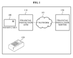
- FIG. 1 is a conceptual diagram illustrating an integrated circuit (IC) chip preventing an identification key leak according to an embodiment of the present invention.
- the IC chip may be included in a smart card 100 that may perform a financial function, for example, credit payment.
- the IC chip to be used for the credit payment may provide an identification key in a form of a time invariant random number, for example, a personal identification number (PIN).
- PIN personal identification number
- the IC chip may include a physically unclonable function (PUF) to provide the PIN based on a circuit configuration.
- PPF physically unclonable function
- the PUF may refer to technology for preventing reproduction of a digital device using a semiconductor processing deviation.
- the technology may relate to obtaining a unique digital value based on a fact that identical circuits have different wire delays, gate delays, and the like based on a process of configuring a circuit.
- the PIN may not be identifiable from the IC chip because the PUF is merely a sequence of identical semiconductor elements and accordingly, a PIN leak may be prevented in advance, despite the smart card 100 being acquired possessed by others.
- the IC chip may transmit the PIN to the ATM 110 only at an initial activation.
- the PIN transmitted to the terminal may be output to the user through a display or by an additional printout method.
- the terminal may not play a role in the providing and storing of the PIN.
- the terminal may perform a simple role of allowing the IC chip to be activated, subsequent to the activation, and passing the provided PIN to the user.
- the PIN passed on to the user may be known, or stored, only by the user.
- the IC chip may cut or completely isolate a path, physically and logically, through which the PIN may be supplied and thus, prevent the PIN from being supplied by any external accesses subsequent to the initial access.
- the IC chip may include at least one fuse and at least one switch.
- the IC chip may apply an overcurrent to the fuse through the switch and cut the fuse to physically block an external access to the PIN.
- the blocking of the external access to the PIN may be performed by the terminal, for example, the ATM 110.
- the terminal may gain access to the IC chip through an input-output interface of the IC chip, read and output the PIN of the IC chip, apply a control signal and a current to a blocking unit disposed between a PIN supply unit and the input-output interface of the IC chip, and block an electrical connection between the PIN supply unit and the input-output interface of the IC chip.
- the terminal may inform a financial institution server 120, through a network 101, of the smart card 100 including the IC chip being issued to allow the smart card 100 to perform a function as a general card through an end terminal 130 used at an affiliated store.
- the financial institution server 120 may not store the PIN provided by the IC chip in a separate server or provide the PIN to a third party, other than the user.
- the PIN of the user may not be leaked by a security attack, for example, hacking into the financial institution server 120 and thus, the financial institution may be exempted from responsibility involved with an illicit use of the card caused by the PIN leak.
- the IC chip may verify whether a PIN input by the user to make use of the IC chip, after the activation, matches the PIN provided by the IC chip.
- the PIN provided by the IC chip may be encoded and stored and thus, the verifying may be performed after encoding the input PIN.
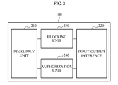
- FIG. 2 is a block diagram illustrating a configuration of an IC chip according to an embodiment of the present invention. Hereinafter, a detailed description of the configuration and a function of the IC chip will be provided with reference to FIG. 2 .
- a smart card 100 may include a PIN supply unit 210, an input-output interface 220, a blocking unit 230, and an authorization unit 240.
- the PIN supply unit 210 performing a function of supplying a PIN may supply, using a PUF as described in the foregoing, the PIN used for authorization when performing a financial function using the IC chip.
- the PIN supply unit 210 may not be limited to the function, but may be configured to store a pre-input PIN upon request by a related operator and supply the stored PIN to be used for authorization when performing the financial function using the IC chip.
- the PIN supply unit 210 may be provided in a form of a nonvolatile memory, for example, an electrically erasable and programmable read only memory (EEPROM).
- EEPROM electrically erasable and programmable read only memory
- the smart card 100 may store a random number of PINs in the EEPROM and supply a PIN as an external input PIN to the user, and authorize the user after comparing the PIN input by the user to the PIN stored in the EEPROM.
- the input-output interface 220 may externally transmit the PIN supplied by the PIN supply unit 210 subsequent to the IC chip being initially accessed.
- the blocking unit 230 may be disposed between the PIN supply unit 210 and the input-output interface 220 and physically block a connection between the PIN supply unit 210 and the input-output interface 220 when the PIN is supplied to an external terminal through the input-output interface 220 subsequent to the IC chip being initially accessed.
- the PIN supply unit 210 supplies the PIN including a PUF
- the PIN may exist simply in a form of hardware in the smart card 100 and a subsequent extraction of the PIN may be permanently enabled.
- the blocking unit 230 may include at least one fuse and at least one switch to apply an overcurrent to the at least one fuse.
- the overcurrent may be a current greater than or equal to a critical current that may melt the at least one fuse.
- the at least one switch may apply the overcurrent to the at least one fuse and physically block the connection between the PIN supply unit 210 and the input-output interface 220.
- a more detailed description of a configuration of the blocking unit 230 will be provided with reference to FIGS. 3 through 6 .
- the authorization unit 240 may compare the PIN supplied by the PIN supply unit 210 to the PIN received from the user, and authorize use of the IC chip when the PIN received from the user matches the PIN supplied by the PIN supply unit 210.
- the authorization unit 240 may authorize the use of the IC chip by encoding and storing the PIN supplied by the PIN supply unit 210, encoding the PIN received from the user, and comparing the PIN received from the user to the encoded and stored PIN.
- PINs to be stored in the authorization unit 240 may be encoded based on an encoding algorithm and thus, it may not be possible, in principle, to find an original PIN prior to the encoding based on the encoded PIN, although verifying whether the PIN input by the user is identical to the encoded and stored PIN may be possible.
- a person finds and possesses the smart card 100 and is able to extract the encoded PIN stored in the authorization unit 240 it may not be possible for the person to use the smart card 100 using the encoded PIN.
- the authorization unit 240 may authorize the use of the IC chip based on the PIN supplied by the PIN supply unit 210 and a special PIN included in the IC chip and used for authorization of the PIN received from the user.
- the PIN supply unit 210 may include a first PUF and a second PUF.
- a PIN supplied by the first PUF may be used as an external input PIN for performing the financial function.
- a value obtained by indexing the PIN supplied by the first PUF to a PIN supplied by the second PUF may be used as a final PIN to authorize the IC chip.
- the PIN supplied by the second PUF may not be extracted by any methods, nor configured to authorize the use of the IC chip through an exclusive or (XOR) gate with the PIN supplied by the first PUF.
- XOR exclusive or
- the authorization unit 240 may allow the smart card 100 to perform a general card function in response to an input by the user. However, when an incorrect PIN is input more than a predetermined number of times, the authorization unit 240 may block an access to the IC chip and not allow the smart card 100 to be used.
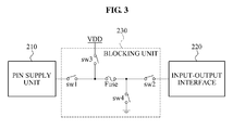
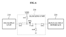
- FIGS. 3 through 6 are circuit diagrams illustrating an operation of a blocking unit 230 of an IC chip according to an embodiment of the present invention.
- the blocking unit 230 may be disposed between a PIN supply unit 210 and an input-output interface 220, and include at least one fuse and at least one switch.
- FIG. 3 illustrates an example of the blocking unit 230 provided with one fuse and four switches, a number and positions of the fuse and the switches may be changed in response to a request by a related operator.
- the blocking unit 230 may control each of the switches at a time of an initial access to the IC chip, for example, to issue a smart card, and allow a PIN supplied by the PIN supply unit 210 to be transmitted externally through the input-output interface 220.
- the blocking unit 230 may control each of the switches to allow an overcurrent to flow in a circuit using a power supply, for example, VDD, to melt the fuse and physically block a connection between the PIN supply unit 210 and the input-output interface 220.
- the blocking unit 230 may control, based on the control signal, each of the switches to allow the overcurrent to flow in the fuse and physically block the connection between the PIN supply unit 210 and the input-output interface 220.
- FIG. 4 illustrates an example in which a PIN supplied by a PIN supply unit 210 is transmitted to an input-output interface 220 by closing a first switch and a second switch.
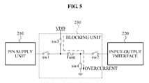
- FIG. 5 illustrates an example in which an overcurrent flows in a fuse by closing a third switch and a fourth switch.
- the blocking unit 230 may generate the control signal or receive the control signal from an external terminal to externally supply the PIN of the PIN supply unit 210 based on the control signal or block the PIN from being supplied externally. For example, as shown in FIG. 4 , when "1" is applied as the control signal, the first switch and the second switch may be closed, but the third switch and the fourth switch may be open. Accordingly, the PIN supplied by the PIN supply unit 210 may be transmitted to the external terminal through the input-output interface 220.
- the first switch and the second switch when "0" is applied as the control signal, the first switch and the second switch may be open, but the third switch and the fourth switch may be closed. Accordingly, as shown in FIG. 6 , although the first switch and the second switch are closed, the overcurrent may flow in the fuse, the connection between the PIN supply unit 210 and the input-output interface 220 may be disconnected due to the melted fuse, and transmission of the PIN may be physically and completely blocked.
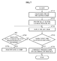
- FIG. 7 is a flowchart illustrating a method of authorizing an IC chip according to an embodiment of the present invention.
- a PIN generated or stored in a PIN supply unit subsequent to an initial access to the IC chip may be transmitted to the external terminal through an input-output interface in operation S710.
- the terms "generate or store” described in the foregoing is interchangeably described herein as “provide” or “supply.”
- the external terminal may display the received PIN on a display or output the received PIN to the user by applying an additional method, for example, a printout method.
- a blocking unit of the IC chip may physically block a connection between the PIN supply unit and the input-output interface and thus, physically block extraction of the PIN.
- an authorization unit of the IC chip may authorize the PIN by verifying whether the received PIN matches the PIN stored in the authorization unit.
- the authorization unit may encode the PIN input by the user and verify the match of the PINs by comparing the encoded PIN input by the user to the encoded and stored PIN.
- the authorization unit may connect the smart card to an external interface in operation S750 and allow the smart card to perform a financial function.
- the authorization unit may inactivate the IC chip by blocking an access to the IC chip.
- the IC chip for preventing a leak of an identification key and the method of authorizing the IC chip disclosed herein is not limited to authorizing the smart card, but may be used for authorizing a micro secure digital (SD) card, a universal subscriber identity module (USIM) card, a credit card, and the like. Also, the discloser may be used to various fields of digital technology requiring user identification and authorization.
- SD micro secure digital
- USIM universal subscriber identity module
- the discloser may be applied, as a gate, to an existing credit card or debit card to activate a smart card chip.
- the discloser may be used without modifications to a method of using an existing financial payment system.
- a user authentication process may be preferentially performed.
- an error message may be output.
- the smart card may be activated and an interface signal sent.
- the IC chip may perform the user authorization and thus, a financial institution, for example, a credit card company, may not need to keep a PIN. Accordingly, the PIN of the user may not be leaked by a security attack, for example, hacking into the financial institution, and thus, the financial institution may disclaim responsibility for unjustifiable use that may occur due to the PIN leak.
- a financial institution for example, a credit card company
Landscapes
- Engineering & Computer Science (AREA)
- Computer Hardware Design (AREA)
- Theoretical Computer Science (AREA)
- Computer Security & Cryptography (AREA)
- Physics & Mathematics (AREA)
- General Physics & Mathematics (AREA)
- General Engineering & Computer Science (AREA)
- Software Systems (AREA)
- Business, Economics & Management (AREA)
- Microelectronics & Electronic Packaging (AREA)
- Computer Networks & Wireless Communication (AREA)
- Signal Processing (AREA)
- Accounting & Taxation (AREA)
- Mathematical Physics (AREA)
- General Business, Economics & Management (AREA)
- Strategic Management (AREA)
- Finance (AREA)
- Storage Device Security (AREA)
- Credit Cards Or The Like (AREA)
Abstract
Description
- The present invention relates to an integrated circuit (IC) chip that may fundamentally prevent exposure of an identification key, for example, a personal identification number (PIN), which is used for authorizing use of the IC chip, and a method of authorizing the IC chip.
- More particularly, the present invention relates to a process of activating a smart card and performing authorization when conducting a financial transaction, and to technology for preventing an external access to identification information, for example, a PIN, in the smart card after the smart card is activated.
- Recently, an integrated circuit (IC) chip having a financial function, for example, a smart card used as a credit card, is being used as a payment means in lieu of cash because of the great convenience provided by use of the IC chip.
- Despite the convenience, there have been reports of accidents, for example, physical duplication of the card and hacking of card numbers, associated with the IC chip having a financial function. Thus, a reliable identification process may be required.
- The identification process may be performed by verifying unique information of a user, for example, a personal identification number (PIN), at a time of payment. Although the PIN may be an only means to authenticate the user, the PIN has a risk of being ineffective due to a PIN leak caused by, for example, hacking into a server of a financial institution.
- For example, Korean Patent Publication No.
10-2007-0084351 - In general, a financial institution, for example, a credit card company, issues a PIN to a user, the financial institution stores the PIN, and payment is authorized when the user correctly inputs the PIN issued by the financial institution. In this case, the financial institution may not be exempted from responsibility for unjustifiable use that may occur when the PIN is revealed by a security attack.
- Thus, a conventional method of issuing and managing a PIN may pose the risk of the PIN leak caused by a security accident including a hacking attack on a financial institution.
- An aspect of the present invention provides an integrated circuit (IC) chip and an authorization method using the IC chip that may prevent a personal identification number (PIN) used for payment using the IC chip having a financial function from being leaked to other people other than a user.
- Another aspect of the present invention provides an IC chip and an authorization method using the IC chip that may be managed by allowing a financial institution to store a PIN on the IC chip, for example, a smart card, instead of issuing the PIN to a user, and disclaim responsibility for leakage of a PIN.
- Still another aspect of the present invention provides an IC chip and an authorization method using the IC chip that may prevent a PIN leak due to the PIN stored in the IC chip and may not require online transmission of the PIN when performing financial payment using the IC chip.
- According to an aspect of the present invention, there is provided an integrated circuit (IC) chip to be used for performing a financial function, including a personal identification number (PIN) supply unit to supply a PIN to be used for authorization when performing the financial function using the IC chip, an input-output interface to transmit the PIN externally, and a blocking unit to physically block a connection between the PIN supply unit and the input-output interface when the PIN is supplied externally through the input-output interface subsequent to the IC chip being initially accessed.
- The blocking unit may include at least one fuse and at least one switch to apply an overcurrent to each of the at least one fuse. Here, the overcurrent may refer to a current greater than or equal to a critical current and able to melt the at least one fuse. When the PIN is supplied externally through the input-output interface subsequent to the IC chip being initially accessed, the at least one switch may apply the overcurrent to the at least one fuse and physically block the connection between the PIN supply unit and the input-output interface.
- The PIN supply unit may include a physically unclonable function (PUF) providing the PIN based on a circuit configuration.
- The IC chip may further include an authorization unit to authorize use of the IC chip when a PIN received from a user matches the PIN supplied by the PIN supply unit as a result of comparing the PIN supplied by the PIN supply unit to the PIN received from the user.
- The authorization unit may authorize the use of the IC chip when the PINs are matched by encoding and storing the PIN supplied by the PIN supply unit, encoding the PIN received from the user, and comparing the PINs.
- The IC chip may further include an authorization unit to authorize the use of the IC chip based on the PIN supplied by the PIN supply unit and a special PIN included in the IC chip and used for authorizing the PIN received from the user.
- The PIN supply unit may store a pre-input PIN and supply the stored PIN to be used for activation of the IC chap, and authorization when performing the financial function using the IC chip.
- According to another aspect of the present invention, there is provided an integrated circuit (IC) chip to be used for performing a financial function, including a personal identification number (PIN) supply unit to store a PIN to be used for authorization when performing the financial function using the IC chip, an input-output interface to transmit the PIN stored in the PIN supply unit to an external terminal when the external terminal gains access to the IC chip, and a blocking unit to physically block a connection between the PIN supply unit and the input-output interface when a control signal is received from the external terminal.
- According to still another aspect of the present invention, there is provided a terminal activating an integrated circuit (IC) chip to be used for performing a financial function. The terminal may gain access to a personal identification number (PIN) supply unit of the IC chip through an input-output interface of the IC chip, read and output the PIN of the IC chip supplied by the PIN supply unit, apply a control signal and a current to a blocking unit disposed between the PIN supply unit of the IC chip and the input-output interface of the IC chip, and block an electrical connection between the PIN supply unit of the IC chip and the input-output interface of the IC chip.
- However, a physical subject performing the blocking of the electrical connection may be the terminal or at least a portion of a peripheral circuit disposed in or along with the IC chip. Although specific mention of the subject performing the blocking of the electrical connection is not made, performance of blocking is not to be construed as being limited to the terminal only.
- According to yet another aspect of the present invention, there is provided an integrated circuit (IC) chip to be used for performing a financial function, including a personal identification number (PIN) supply unit to supply a PIN to be used for authorization when performing the financial function using the IC chip, an input-output interface to transmit the PIN supplied by the PIN supply unit when an external terminal gains access to the IC chip, an authorization unit to authorize, when a PIN is input to perform the financial function using the IC chip, the input PIN as a result of comparing the input PIN to the PIN supplied by the PIN supply unit and block the access to the IC chip when an incorrect PIN is input more than predetermined number of times, and a blocking unit to physically block a connection between the PIN supply unit and the input-output interface when the PIN is supplied externally through the input-output interface subsequent to the IC chip being initially accessed.
- According to further another aspect of the present invention, there is provided a method of authorizing an integrated circuit (IC) chip to be used for performing a financial function, including supplying a PIN for authorization when performing the financial function, transmitting the supplied PIN externally subsequent to the IC chip being initially accessed, physically blocking extraction of the PIN, and authorizing use of the IC chip when a PIN received from a user matches the supplied PIN as a result of comparing the supplied PIN to the PIN received from the user.
- In a case of payment performed using an integrated circuit (IC) chip having a financial function, a financial institution, for example, a credit card company, may not be required to keep a personal identification number (PIN) used for identifying a user and thus, a PIN leakage may be fundamentally prevented even from a security attack, for example, hacking into the financial institution.
- Thus, the financial institution may disclaim a responsibility for unjustifiable use of a card that may be caused by the PIN leakage.
-
-
FIG. 1 is a conceptual diagram illustrating an integrated circuit (IC) chip preventing an identification key leak according to an embodiment of the present invention. -
FIG. 2 is a block diagram illustrating a configuration of an IC chip according to an embodiment of the present invention. -
FIGS. 3 through 6 are circuit diagrams illustrating operation of a blocking unit of an IC chip according to an embodiment of the present invention. -
FIG. 7 is a flowchart illustrating a method of authorizing an IC chip according to an embodiment of the present invention. - Reference will now be made in detail to embodiments of the present invention, examples of which are illustrated in the accompanying drawings, wherein like reference numerals refer to the like elements throughout. The embodiments are described below in order to explain the present invention by referring to the figures.
-
FIG. 1 is a conceptual diagram illustrating an integrated circuit (IC) chip preventing an identification key leak according to an embodiment of the present invention. - Referring to
FIG. 1 , the IC chip may be included in asmart card 100 that may perform a financial function, for example, credit payment. The IC chip to be used for the credit payment may provide an identification key in a form of a time invariant random number, for example, a personal identification number (PIN). The IC chip may include a physically unclonable function (PUF) to provide the PIN based on a circuit configuration. - The PUF may refer to technology for preventing reproduction of a digital device using a semiconductor processing deviation. The technology may relate to obtaining a unique digital value based on a fact that identical circuits have different wire delays, gate delays, and the like based on a process of configuring a circuit. In a case of providing the PIN using the PUF, the PIN may not be identifiable from the IC chip because the PUF is merely a sequence of identical semiconductor elements and accordingly, a PIN leak may be prevented in advance, despite the
smart card 100 being acquired possessed by others. - When a user activates the IC chip in a terminal, for example, an automated teller machine (ATM) 110 of a financial institution, the IC chip may transmit the PIN to the
ATM 110 only at an initial activation. The PIN transmitted to the terminal may be output to the user through a display or by an additional printout method. Here, the terminal may not play a role in the providing and storing of the PIN. However, the terminal may perform a simple role of allowing the IC chip to be activated, subsequent to the activation, and passing the provided PIN to the user. - The PIN passed on to the user may be known, or stored, only by the user. According to an embodiment, the IC chip may cut or completely isolate a path, physically and logically, through which the PIN may be supplied and thus, prevent the PIN from being supplied by any external accesses subsequent to the initial access.
- To perform the cutting or isolating, the IC chip may include at least one fuse and at least one switch. Here, subsequent to the initial access to the PIN, the IC chip may apply an overcurrent to the fuse through the switch and cut the fuse to physically block an external access to the PIN.
- According to another embodiment, the blocking of the external access to the PIN may be performed by the terminal, for example, the
ATM 110. Here, the terminal may gain access to the IC chip through an input-output interface of the IC chip, read and output the PIN of the IC chip, apply a control signal and a current to a blocking unit disposed between a PIN supply unit and the input-output interface of the IC chip, and block an electrical connection between the PIN supply unit and the input-output interface of the IC chip. - Subsequently, the terminal may inform a
financial institution server 120, through anetwork 101, of thesmart card 100 including the IC chip being issued to allow thesmart card 100 to perform a function as a general card through anend terminal 130 used at an affiliated store. - Here, the
financial institution server 120 may not store the PIN provided by the IC chip in a separate server or provide the PIN to a third party, other than the user. Thus, the PIN of the user may not be leaked by a security attack, for example, hacking into thefinancial institution server 120 and thus, the financial institution may be exempted from responsibility involved with an illicit use of the card caused by the PIN leak. - According to an embodiment, in order to authorize use of the
smart card 100, the IC chip may verify whether a PIN input by the user to make use of the IC chip, after the activation, matches the PIN provided by the IC chip. Here, the PIN provided by the IC chip may be encoded and stored and thus, the verifying may be performed after encoding the input PIN. -
FIG. 2 is a block diagram illustrating a configuration of an IC chip according to an embodiment of the present invention. Hereinafter, a detailed description of the configuration and a function of the IC chip will be provided with reference toFIG. 2 . - A
smart card 100 may include aPIN supply unit 210, an input-output interface 220, ablocking unit 230, and anauthorization unit 240. - The
PIN supply unit 210 performing a function of supplying a PIN may supply, using a PUF as described in the foregoing, the PIN used for authorization when performing a financial function using the IC chip. However, thePIN supply unit 210 may not be limited to the function, but may be configured to store a pre-input PIN upon request by a related operator and supply the stored PIN to be used for authorization when performing the financial function using the IC chip. For example, thePIN supply unit 210 may be provided in a form of a nonvolatile memory, for example, an electrically erasable and programmable read only memory (EEPROM). Here, thesmart card 100 may store a random number of PINs in the EEPROM and supply a PIN as an external input PIN to the user, and authorize the user after comparing the PIN input by the user to the PIN stored in the EEPROM. - The input-
output interface 220 may externally transmit the PIN supplied by thePIN supply unit 210 subsequent to the IC chip being initially accessed. - According to an embodiment, the blocking
unit 230 may be disposed between thePIN supply unit 210 and the input-output interface 220 and physically block a connection between thePIN supply unit 210 and the input-output interface 220 when the PIN is supplied to an external terminal through the input-output interface 220 subsequent to the IC chip being initially accessed. - Thus, when the
PIN supply unit 210 supplies the PIN including a PUF, the PIN may exist simply in a form of hardware in thesmart card 100 and a subsequent extraction of the PIN may be permanently enabled. - According to an embodiment, the blocking
unit 230 may include at least one fuse and at least one switch to apply an overcurrent to the at least one fuse. Here, the overcurrent may be a current greater than or equal to a critical current that may melt the at least one fuse. - Here, when the PIN is supplied externally through the input-
output interface 220 subsequent to the IC chip being initially accessed, the at least one switch may apply the overcurrent to the at least one fuse and physically block the connection between thePIN supply unit 210 and the input-output interface 220. A more detailed description of a configuration of theblocking unit 230 will be provided with reference toFIGS. 3 through 6 . - When the
authorization unit 240 receives a PIN input by the user through the input-output interface 230 from the external terminal, for example, a financial institution ATM, theauthorization unit 240 may compare the PIN supplied by thePIN supply unit 210 to the PIN received from the user, and authorize use of the IC chip when the PIN received from the user matches the PIN supplied by thePIN supply unit 210. - Here, the
authorization unit 240 may authorize the use of the IC chip by encoding and storing the PIN supplied by thePIN supply unit 210, encoding the PIN received from the user, and comparing the PIN received from the user to the encoded and stored PIN. - Here, PINs to be stored in the
authorization unit 240 may be encoded based on an encoding algorithm and thus, it may not be possible, in principle, to find an original PIN prior to the encoding based on the encoded PIN, although verifying whether the PIN input by the user is identical to the encoded and stored PIN may be possible. Thus, although a person finds and possesses thesmart card 100 and is able to extract the encoded PIN stored in theauthorization unit 240, it may not be possible for the person to use thesmart card 100 using the encoded PIN. - Also, the
authorization unit 240 may authorize the use of the IC chip based on the PIN supplied by thePIN supply unit 210 and a special PIN included in the IC chip and used for authorization of the PIN received from the user. For example, thePIN supply unit 210 may include a first PUF and a second PUF. Here, a PIN supplied by the first PUF may be used as an external input PIN for performing the financial function. Also, a value obtained by indexing the PIN supplied by the first PUF to a PIN supplied by the second PUF may be used as a final PIN to authorize the IC chip. Here, the PIN supplied by the second PUF may not be extracted by any methods, nor configured to authorize the use of the IC chip through an exclusive or (XOR) gate with the PIN supplied by the first PUF. Thus, although the PIN supplied by the first PUF is leaked due to inattentiveness of the user, it may not be possible to reproduce the final PIN. - When the PIN input by the user is authorized, the
authorization unit 240 may allow thesmart card 100 to perform a general card function in response to an input by the user. However, when an incorrect PIN is input more than a predetermined number of times, theauthorization unit 240 may block an access to the IC chip and not allow thesmart card 100 to be used. -
FIGS. 3 through 6 are circuit diagrams illustrating an operation of ablocking unit 230 of an IC chip according to an embodiment of the present invention. - Referring to
FIG. 3 , the blockingunit 230 may be disposed between aPIN supply unit 210 and an input-output interface 220, and include at least one fuse and at least one switch. AlthoughFIG. 3 illustrates an example of theblocking unit 230 provided with one fuse and four switches, a number and positions of the fuse and the switches may be changed in response to a request by a related operator. - The blocking
unit 230 may control each of the switches at a time of an initial access to the IC chip, for example, to issue a smart card, and allow a PIN supplied by thePIN supply unit 210 to be transmitted externally through the input-output interface 220. When the PIN is transmitted externally, the blockingunit 230 may control each of the switches to allow an overcurrent to flow in a circuit using a power supply, for example, VDD, to melt the fuse and physically block a connection between thePIN supply unit 210 and the input-output interface 220. - When a control signal is received from an external terminal, the blocking
unit 230 may control, based on the control signal, each of the switches to allow the overcurrent to flow in the fuse and physically block the connection between thePIN supply unit 210 and the input-output interface 220. -
FIG. 4 illustrates an example in which a PIN supplied by aPIN supply unit 210 is transmitted to an input-output interface 220 by closing a first switch and a second switch.FIG. 5 illustrates an example in which an overcurrent flows in a fuse by closing a third switch and a fourth switch. - The blocking
unit 230 may generate the control signal or receive the control signal from an external terminal to externally supply the PIN of thePIN supply unit 210 based on the control signal or block the PIN from being supplied externally. For example, as shown inFIG. 4 , when "1" is applied as the control signal, the first switch and the second switch may be closed, but the third switch and the fourth switch may be open. Accordingly, the PIN supplied by thePIN supply unit 210 may be transmitted to the external terminal through the input-output interface 220. - Conversely, as shown in
FIG. 5 , when "0" is applied as the control signal, the first switch and the second switch may be open, but the third switch and the fourth switch may be closed. Accordingly, as shown inFIG. 6 , although the first switch and the second switch are closed, the overcurrent may flow in the fuse, the connection between thePIN supply unit 210 and the input-output interface 220 may be disconnected due to the melted fuse, and transmission of the PIN may be physically and completely blocked. -
FIG. 7 is a flowchart illustrating a method of authorizing an IC chip according to an embodiment of the present invention. - When a user is issued a smart card including the IC chip through an external terminal, a PIN generated or stored in a PIN supply unit subsequent to an initial access to the IC chip may be transmitted to the external terminal through an input-output interface in operation S710. Here, the terms "generate or store" described in the foregoing is interchangeably described herein as "provide" or "supply." The external terminal may display the received PIN on a display or output the received PIN to the user by applying an additional method, for example, a printout method.
- In operation S720, a blocking unit of the IC chip may physically block a connection between the PIN supply unit and the input-output interface and thus, physically block extraction of the PIN.
- When the user uses the smart card registered using the method and the user inputs a PIN to an end terminal of an affiliated store in operation S730, an authorization unit of the IC chip may authorize the PIN by verifying whether the received PIN matches the PIN stored in the authorization unit. Here, when the PIN stored in the authorization unit is encoded and stored, the authorization unit may encode the PIN input by the user and verify the match of the PINs by comparing the encoded PIN input by the user to the encoded and stored PIN.
- When the authorization unit determines that the PINs are matched, the authorization unit may connect the smart card to an external interface in operation S750 and allow the smart card to perform a financial function.
- However, when an incorrect PIN is input by the user more than a predetermined number of times, for example, three times, in operation S760, the authorization unit may inactivate the IC chip by blocking an access to the IC chip.
- The IC chip for preventing a leak of an identification key and the method of authorizing the IC chip disclosed herein is not limited to authorizing the smart card, but may be used for authorizing a micro secure digital (SD) card, a universal subscriber identity module (USIM) card, a credit card, and the like. Also, the discloser may be used to various fields of digital technology requiring user identification and authorization.
- Also, the discloser may be applied, as a gate, to an existing credit card or debit card to activate a smart card chip. Here, the discloser may be used without modifications to a method of using an existing financial payment system. For example, when the IC chip according to an embodiment of the present invention is used for a smart card, a user authentication process may be preferentially performed. Here, when the user authentication fails, an error message may be output. When the user authentication succeeds, the smart card may be activated and an interface signal sent.
- Further, according to an embodiment of the present invention, the IC chip may perform the user authorization and thus, a financial institution, for example, a credit card company, may not need to keep a PIN. Accordingly, the PIN of the user may not be leaked by a security attack, for example, hacking into the financial institution, and thus, the financial institution may disclaim responsibility for unjustifiable use that may occur due to the PIN leak.
- Although a few embodiments of the present invention have been shown and described, the present invention is not limited to the described embodiments. Instead, it would be appreciated by those skilled in the art that changes may be made to these embodiments without departing from the principles and spirit of the invention, the scope of which is defined by the claims and their equivalents.
- 100:
- Smart card
- 101:
- Network
- 110:
- Financial institution ATM
- 120:
- Financial institution server
Claims (14)
- An integrated circuit (IC) chip to be used for performing a financial function, the IC chip comprising:a personal identification number (PIN) supply unit to supply a PIN to be used for authorization when performing the financial function using the IC chip;an input-output interface to transmit the PIN externally; anda blocking unit to physically block a connection between the PIN supply unit and the input-output interface when the PIN is transmitted externally through the input-output interface subsequent to the IC chip being initially accessed.
- The IC chip of claim 1, wherein the blocking unit comprises at least one fuse and at least one switch to apply an overcurrent to each of the at least one fuse, and
wherein the overrcurrent is a current greater than or equal to a critical current and is able to melt the at least one fuse, and
wherein, when the PIN is transmitted externally through the input-output interface subsequent to the IC chip being initially accessed, the at least one switch applies the overcurrent to the at least one fuse and physically blocks the connection between the PIN supply unit and the input-output interface. - The IC chip of claim 1, wherein the PIN supply unit comprises a physically unclonable function (PUF) providing the PIN using a semiconductor manufacturing process deviation.
- The IC chip of claim 1, further comprising:an authorization unit to authorize use of the IC chip when a PIN received from a user matches the PIN supplied by the PIN supply unit as a result of comparing the PIN supplied by the PIN supply unit to the PIN received from the user.
- The IC chip of claim 4, wherein the authorization unit authorizes use of the IC chip when the PINs are matched by encoding and storing the PIN supplied by the PIN supply unit, encoding the PIN received from the user, and comparing the PINs.
- The IC chip of claim 1, further comprising:an authorization unit to authorize use of the IC chip based on the PIN supplied by the PIN supply unit and a special PIN comprised in the IC chip and used for authorizing a PIN received from a user.
- The IC chip of claim 1, wherein the PIN supply unit stores a pre-input PIN and supplies the stored PIN to be used for authorization when performing the financial function using the IC chip.
- An integrated circuit (IC) chip to be used for performing a financial function, the IC chip comprising:a personal identification number (PIN) supply unit to store a PIN to be used for authorization when performing the financial function using the IC chip;an input-output interface to transmit the PIN stored in the PIN supply unit to an external terminal when the external terminal gains access to the IC chip; anda blocking unit to physically block a connection between the PIN supply unit and the input-output interface when a control signal is received from the external terminal.
- The IC chip of claim 8, wherein the blocking unit comprises at least one fuse and a switch to apply a current to the at least one fuse and, when the control signal is received, physically blocks the connection between the PIN supply unit and the input-output interface by applying an overcurrent that is greater than or equal to a critical current and is able to melt each of the at least one fuse, through the switch.
- The IC chip of claim 8, further comprising:an authorization unit to authorize use of the IC chip when a PIN received from a user matches the PIN supplied by the PIN supply unit as a result of comparing the PIN supplied by the PIN supply unit to the PIN received from the user.
- A terminal activating an integrated circuit (IC) chip to be used for performing a financial function, the terminal:gains access to a personal identification number (PIN) supply unit of the IC chip through an input-output interface of the IC chip and reads and outputs a PIN of the IC chip supplied by the PIN supply unit; andapplies a control signal and a current to a blocking unit disposed between the PIN supply unit of the IC chip and the input-output interface of the IC chip, and blocks an electrical connection between the PIN supply unit of the IC chip and the input-output interface of the IC chip.
- An integrated circuit (IC) chip to be used for performing a financial function, the IC chip comprising:a personal identification number (PIN) supply unit to supply a PIN to be used for authorization when performing the financial function using the IC chip;an input-output interface to transmit the PIN supplied by the PIN supply unit to an external terminal when the external terminal gains access to the IC chip;an authorization unit to authorize, when a PIN is input to perform the financial function using the IC chip, the input PIN as a result of comparing the input PIN to the PIN supplied by the PIN supply unit, and block an access to the IC chip when an incorrect PIN is input more than a predetermined number of times; anda blocking unit to physically block a connection between the PIN supply unit and the input-output interface when the PIN is supplied externally through the input-output interface subsequent to the IC chip being initially accessed.
- The IC chip of claim 12, wherein the blocking unit comprises at least one fuse and at least one switch to apply an overcurrent to each of the at least one fuse, and
wherein the overcurrent is a current greater than or equal to a critical current and is able to melt the at least one fuse, and
wherein the at least one switch applies the overcurrent to the at least one fuse and physically blocks the connection between the PIN supply unit and the input-output interface when the PIN is transmitted externally through the input-output interface subsequent to the IC chip being initially accessed. - A method of authorizing an integrated circuit (IC) chip to be used for performing a financial function, the method comprising:supplying a personal identification number (PIN) for authorization when performing the financial function;transmitting the supplied PIN externally, subsequent to the IC chip being initially accessed;physically blocking extraction of the PIN; andauthorizing use of the IC chip when a PIN received from a user matches the supplied PIN as a result of comparing the supplied PIN to the PIN received from the user.
Applications Claiming Priority (2)
| Application Number | Priority Date | Filing Date | Title |
|---|---|---|---|
| KR20110077271A KR101080511B1 (en) | 2011-08-03 | 2011-08-03 | IC chip prevents identification key leakage and its authentication method |
| PCT/KR2011/005830 WO2013018947A1 (en) | 2011-08-03 | 2011-08-10 | Ic chip for preventing identification key leak and authorization method thereof |
Publications (3)
| Publication Number | Publication Date |
|---|---|
| EP2741239A1 true EP2741239A1 (en) | 2014-06-11 |
| EP2741239A4 EP2741239A4 (en) | 2015-04-08 |
| EP2741239B1 EP2741239B1 (en) | 2020-12-23 |
Family
ID=45397231
Family Applications (1)
| Application Number | Title | Priority Date | Filing Date |
|---|---|---|---|
| EP11870389.1A Active EP2741239B1 (en) | 2011-08-03 | 2011-08-10 | Ic chip for preventing identification key leak and authorization method thereof |
Country Status (6)
| Country | Link |
|---|---|
| US (1) | US9996836B2 (en) |
| EP (1) | EP2741239B1 (en) |
| JP (2) | JP2014522180A (en) |
| KR (1) | KR101080511B1 (en) |
| CN (1) | CN104025122A (en) |
| WO (1) | WO2013018947A1 (en) |
Families Citing this family (12)
| Publication number | Priority date | Publication date | Assignee | Title |
|---|---|---|---|---|
| US8885819B2 (en) * | 2012-12-27 | 2014-11-11 | Intel Corporation | Fuse attestation to secure the provisioning of secret keys during integrated circuit manufacturing |
| WO2015012667A1 (en) | 2013-07-26 | 2015-01-29 | (주) 아이씨티케이 | Device and method for testing randomness |
| KR101495448B1 (en) | 2013-10-29 | 2015-02-26 | (주) 아이씨티케이 | Integrated circuit chip for user authentication and autentication method |
| JP6587188B2 (en) * | 2015-06-18 | 2019-10-09 | パナソニックIpマネジメント株式会社 | Random number processing apparatus, integrated circuit card, and random number processing method |
| WO2017078427A1 (en) * | 2015-11-03 | 2017-05-11 | (주) 아이씨티케이 | Security apparatus and operation method thereof |
| US10476680B2 (en) | 2016-02-03 | 2019-11-12 | Ememory Technology Inc. | Electronic device with self-protection and anti-cloning capabilities and related method |
| US10122538B2 (en) * | 2016-10-12 | 2018-11-06 | Ememory Technology Inc. | Antifuse physically unclonable function unit and associated control method |
| US10614254B2 (en) | 2017-12-12 | 2020-04-07 | John Almeida | Virus immune computer system and method |
| US10642970B2 (en) * | 2017-12-12 | 2020-05-05 | John Almeida | Virus immune computer system and method |
| US10592697B1 (en) | 2017-12-12 | 2020-03-17 | John Almeida | Virus immune computer system and method |
| US11516028B2 (en) | 2019-12-24 | 2022-11-29 | CERA Licensing Limited | Temperature sensing physical unclonable function (PUF) authentication system |
| GB201919297D0 (en) | 2019-12-24 | 2020-02-05 | Aronson Bill | Temperature sensing physical unclonable function (puf) authenication system |
Family Cites Families (21)
| Publication number | Priority date | Publication date | Assignee | Title |
|---|---|---|---|---|
| JPH04258898A (en) * | 1991-02-13 | 1992-09-14 | Nec Corp | Hybrid integrated circuit and its production method |
| US5786587A (en) * | 1995-08-10 | 1998-07-28 | American Bank Note Holographics, Inc. | Enhancement of chip card security |
| JP3689213B2 (en) * | 1997-01-21 | 2005-08-31 | ローム株式会社 | Non-contact IC card |
| US6257486B1 (en) * | 1998-11-23 | 2001-07-10 | Cardis Research & Development Ltd. | Smart card pin system, card, and reader |
| US6281028B1 (en) * | 1999-09-30 | 2001-08-28 | Advanced Micro Devices, Inc. | LED alignment points for semiconductor die |
| DK174672B1 (en) * | 1999-11-09 | 2003-08-25 | Orange As | Electronic identification code delivery system |
| US6641050B2 (en) * | 2001-11-06 | 2003-11-04 | International Business Machines Corporation | Secure credit card |
| JP2003303309A (en) * | 2002-04-09 | 2003-10-24 | Hitachi Ltd | Transaction system and transaction method using card, computer program for processing for transaction |
| AU2003283760A1 (en) | 2003-01-14 | 2004-08-10 | Koninklijke Philips Electronics N.V. | Method and terminal for detecting fake and/or modified smart card |
| CN2613828Y (en) * | 2003-04-22 | 2004-04-28 | 上海华园微电子技术有限公司 | Safety protector in IC card |
| JP4639676B2 (en) | 2004-07-21 | 2011-02-23 | 株式会社日立製作所 | Rental server system |
| CN100573569C (en) * | 2004-09-10 | 2009-12-23 | 株式会社半导体能源研究所 | Semiconductor device with a plurality of semiconductor chips |
| KR100675423B1 (en) | 2004-09-16 | 2007-01-29 | 주식회사 국민은행 | IC card with electronic bankbook and public certificate, processing terminal and card issuing server |
| JP2008517508A (en) | 2004-10-18 | 2008-05-22 | コーニンクレッカ フィリップス エレクトロニクス エヌ ヴィ | Secure sensor chip |
| CN100565562C (en) | 2007-10-15 | 2009-12-02 | 北京派瑞根科技开发有限公司 | Electronic label security authentication method |
| BRPI0912057B1 (en) * | 2008-08-08 | 2020-09-15 | Assa Abloy Ab | DIRECTIONAL SENSOR MECHANISM AND COMMUNICATION AUTHENTICATION |
| WO2010035202A1 (en) * | 2008-09-26 | 2010-04-01 | Koninklijke Philips Electronics N.V. | Authenticating a device and a user |
| CN102265395B (en) * | 2008-12-29 | 2013-10-16 | Nxp股份有限公司 | Physical structure for use in physical unclonable function |
| JP3160554U (en) * | 2010-03-15 | 2010-07-01 | 俊則 清水 | Certification system |
| CN101854357B (en) * | 2010-05-10 | 2013-09-04 | 深圳市中科新业信息科技发展有限公司 | Method and system for monitoring network authentication |
| US8868923B1 (en) * | 2010-07-28 | 2014-10-21 | Sandia Corporation | Multi-factor authentication |
-
2011
- 2011-08-03 KR KR20110077271A patent/KR101080511B1/en active Active
- 2011-08-10 JP JP2014523825A patent/JP2014522180A/en active Pending
- 2011-08-10 EP EP11870389.1A patent/EP2741239B1/en active Active
- 2011-08-10 US US14/236,733 patent/US9996836B2/en active Active
- 2011-08-10 CN CN201180072740.0A patent/CN104025122A/en active Pending
- 2011-08-10 WO PCT/KR2011/005830 patent/WO2013018947A1/en not_active Ceased
-
2015
- 2015-11-16 JP JP2015223639A patent/JP6204439B2/en active Active
Also Published As
| Publication number | Publication date |
|---|---|
| JP2014522180A (en) | 2014-08-28 |
| US9996836B2 (en) | 2018-06-12 |
| WO2013018947A1 (en) | 2013-02-07 |
| CN104025122A (en) | 2014-09-03 |
| EP2741239B1 (en) | 2020-12-23 |
| EP2741239A4 (en) | 2015-04-08 |
| JP2016048951A (en) | 2016-04-07 |
| US20150127537A1 (en) | 2015-05-07 |
| JP6204439B2 (en) | 2017-09-27 |
| KR101080511B1 (en) | 2011-11-04 |
Similar Documents
| Publication | Publication Date | Title |
|---|---|---|
| EP2741239B1 (en) | Ic chip for preventing identification key leak and authorization method thereof | |
| EP3807831B1 (en) | Method and system to create a trusted record or message and usage for a secure activation or strong customer authentication | |
| AU2023202708B2 (en) | Secure authentication based on identity data stored in a contactless card | |
| US11941621B2 (en) | Secure authentication based on passport data stored in a contactless card | |
| WO2018096559A1 (en) | System and method for translation and authentication of secure pin and sensitive data | |
| JP2024528476A (en) | Cryptographic authentication for controlling access to storage devices | |
| EP4222922B1 (en) | Method for managing a pin code in a biometric smart card | |
| CN102034307A (en) | Electronic wallet-based dynamic password authentication system and method | |
| KR101495448B1 (en) | Integrated circuit chip for user authentication and autentication method | |
| KR101103189B1 (en) | Method and system for issuing a public certificate using universal subscriber identification module information and recording medium therefor | |
| US11200571B2 (en) | Method of controlling an electronic device and corresponding electronic device | |
| KR20200103615A (en) | System and Method for Identification Based on Finanace Card Possessed by User | |
| HK40058340A (en) | Secure authentication based on identity data stored in a contactless card | |
| KR20150050335A (en) | Integrated circuit chip for user authentication and autentication method | |
| KR101298099B1 (en) | Des board with multi-key and methof for setting the des board | |
| HK40068620A (en) | Method for secure authentication, computing apparatus and storage medium |
Legal Events
| Date | Code | Title | Description |
|---|---|---|---|
| PUAI | Public reference made under article 153(3) epc to a published international application that has entered the european phase |
Free format text: ORIGINAL CODE: 0009012 |
|
| 17P | Request for examination filed |
Effective date: 20140228 |
|
| AK | Designated contracting states |
Kind code of ref document: A1 Designated state(s): AL AT BE BG CH CY CZ DE DK EE ES FI FR GB GR HR HU IE IS IT LI LT LU LV MC MK MT NL NO PL PT RO RS SE SI SK SM TR |
|
| DAX | Request for extension of the european patent (deleted) | ||
| RA4 | Supplementary search report drawn up and despatched (corrected) |
Effective date: 20150311 |
|
| RIC1 | Information provided on ipc code assigned before grant |
Ipc: G06K 19/073 20060101ALI20150305BHEP Ipc: G06K 19/07 20060101AFI20150305BHEP Ipc: G06K 17/00 20060101ALI20150305BHEP Ipc: H04L 9/32 20060101ALI20150305BHEP |
|
| RAP1 | Party data changed (applicant data changed or rights of an application transferred) |
Owner name: ICTK HOLDINGS CO., LTD. |
|
| STAA | Information on the status of an ep patent application or granted ep patent |
Free format text: STATUS: EXAMINATION IS IN PROGRESS |
|
| 17Q | First examination report despatched |
Effective date: 20200226 |
|
| REG | Reference to a national code |
Ref country code: DE Ref legal event code: R079 Ref document number: 602011069772 Country of ref document: DE Free format text: PREVIOUS MAIN CLASS: G06K0019070000 Ipc: G06F0021770000 |
|
| GRAP | Despatch of communication of intention to grant a patent |
Free format text: ORIGINAL CODE: EPIDOSNIGR1 |
|
| STAA | Information on the status of an ep patent application or granted ep patent |
Free format text: STATUS: GRANT OF PATENT IS INTENDED |
|
| RIC1 | Information provided on ipc code assigned before grant |
Ipc: G06F 21/77 20130101AFI20200617BHEP Ipc: G06F 21/85 20130101ALI20200617BHEP Ipc: G06K 19/073 20060101ALI20200617BHEP Ipc: H04L 9/32 20060101ALI20200617BHEP |
|
| INTG | Intention to grant announced |
Effective date: 20200716 |
|
| GRAS | Grant fee paid |
Free format text: ORIGINAL CODE: EPIDOSNIGR3 |
|
| GRAA | (expected) grant |
Free format text: ORIGINAL CODE: 0009210 |
|
| STAA | Information on the status of an ep patent application or granted ep patent |
Free format text: STATUS: THE PATENT HAS BEEN GRANTED |
|
| AK | Designated contracting states |
Kind code of ref document: B1 Designated state(s): AL AT BE BG CH CY CZ DE DK EE ES FI FR GB GR HR HU IE IS IT LI LT LU LV MC MK MT NL NO PL PT RO RS SE SI SK SM TR |
|
| REG | Reference to a national code |
Ref country code: GB Ref legal event code: FG4D |
|
| REG | Reference to a national code |
Ref country code: DE Ref legal event code: R096 Ref document number: 602011069772 Country of ref document: DE |
|
| REG | Reference to a national code |
Ref country code: AT Ref legal event code: REF Ref document number: 1348431 Country of ref document: AT Kind code of ref document: T Effective date: 20210115 |
|
| REG | Reference to a national code |
Ref country code: IE Ref legal event code: FG4D |
|
| PG25 | Lapsed in a contracting state [announced via postgrant information from national office to epo] |
Ref country code: GR Free format text: LAPSE BECAUSE OF FAILURE TO SUBMIT A TRANSLATION OF THE DESCRIPTION OR TO PAY THE FEE WITHIN THE PRESCRIBED TIME-LIMIT Effective date: 20210324 Ref country code: RS Free format text: LAPSE BECAUSE OF FAILURE TO SUBMIT A TRANSLATION OF THE DESCRIPTION OR TO PAY THE FEE WITHIN THE PRESCRIBED TIME-LIMIT Effective date: 20201223 Ref country code: FI Free format text: LAPSE BECAUSE OF FAILURE TO SUBMIT A TRANSLATION OF THE DESCRIPTION OR TO PAY THE FEE WITHIN THE PRESCRIBED TIME-LIMIT Effective date: 20201223 Ref country code: NO Free format text: LAPSE BECAUSE OF FAILURE TO SUBMIT A TRANSLATION OF THE DESCRIPTION OR TO PAY THE FEE WITHIN THE PRESCRIBED TIME-LIMIT Effective date: 20210323 |
|
| REG | Reference to a national code |
Ref country code: AT Ref legal event code: MK05 Ref document number: 1348431 Country of ref document: AT Kind code of ref document: T Effective date: 20201223 |
|
| REG | Reference to a national code |
Ref country code: NL Ref legal event code: MP Effective date: 20201223 |
|
| PG25 | Lapsed in a contracting state [announced via postgrant information from national office to epo] |
Ref country code: SE Free format text: LAPSE BECAUSE OF FAILURE TO SUBMIT A TRANSLATION OF THE DESCRIPTION OR TO PAY THE FEE WITHIN THE PRESCRIBED TIME-LIMIT Effective date: 20201223 Ref country code: LV Free format text: LAPSE BECAUSE OF FAILURE TO SUBMIT A TRANSLATION OF THE DESCRIPTION OR TO PAY THE FEE WITHIN THE PRESCRIBED TIME-LIMIT Effective date: 20201223 Ref country code: BG Free format text: LAPSE BECAUSE OF FAILURE TO SUBMIT A TRANSLATION OF THE DESCRIPTION OR TO PAY THE FEE WITHIN THE PRESCRIBED TIME-LIMIT Effective date: 20210323 |
|
| PG25 | Lapsed in a contracting state [announced via postgrant information from national office to epo] |
Ref country code: NL Free format text: LAPSE BECAUSE OF FAILURE TO SUBMIT A TRANSLATION OF THE DESCRIPTION OR TO PAY THE FEE WITHIN THE PRESCRIBED TIME-LIMIT Effective date: 20201223 Ref country code: HR Free format text: LAPSE BECAUSE OF FAILURE TO SUBMIT A TRANSLATION OF THE DESCRIPTION OR TO PAY THE FEE WITHIN THE PRESCRIBED TIME-LIMIT Effective date: 20201223 |
|
| REG | Reference to a national code |
Ref country code: LT Ref legal event code: MG9D |
|
| PG25 | Lapsed in a contracting state [announced via postgrant information from national office to epo] |
Ref country code: PT Free format text: LAPSE BECAUSE OF FAILURE TO SUBMIT A TRANSLATION OF THE DESCRIPTION OR TO PAY THE FEE WITHIN THE PRESCRIBED TIME-LIMIT Effective date: 20210423 Ref country code: SK Free format text: LAPSE BECAUSE OF FAILURE TO SUBMIT A TRANSLATION OF THE DESCRIPTION OR TO PAY THE FEE WITHIN THE PRESCRIBED TIME-LIMIT Effective date: 20201223 Ref country code: RO Free format text: LAPSE BECAUSE OF FAILURE TO SUBMIT A TRANSLATION OF THE DESCRIPTION OR TO PAY THE FEE WITHIN THE PRESCRIBED TIME-LIMIT Effective date: 20201223 Ref country code: LT Free format text: LAPSE BECAUSE OF FAILURE TO SUBMIT A TRANSLATION OF THE DESCRIPTION OR TO PAY THE FEE WITHIN THE PRESCRIBED TIME-LIMIT Effective date: 20201223 Ref country code: SM Free format text: LAPSE BECAUSE OF FAILURE TO SUBMIT A TRANSLATION OF THE DESCRIPTION OR TO PAY THE FEE WITHIN THE PRESCRIBED TIME-LIMIT Effective date: 20201223 Ref country code: CZ Free format text: LAPSE BECAUSE OF FAILURE TO SUBMIT A TRANSLATION OF THE DESCRIPTION OR TO PAY THE FEE WITHIN THE PRESCRIBED TIME-LIMIT Effective date: 20201223 Ref country code: EE Free format text: LAPSE BECAUSE OF FAILURE TO SUBMIT A TRANSLATION OF THE DESCRIPTION OR TO PAY THE FEE WITHIN THE PRESCRIBED TIME-LIMIT Effective date: 20201223 |
|
| PG25 | Lapsed in a contracting state [announced via postgrant information from national office to epo] |
Ref country code: AT Free format text: LAPSE BECAUSE OF FAILURE TO SUBMIT A TRANSLATION OF THE DESCRIPTION OR TO PAY THE FEE WITHIN THE PRESCRIBED TIME-LIMIT Effective date: 20201223 Ref country code: PL Free format text: LAPSE BECAUSE OF FAILURE TO SUBMIT A TRANSLATION OF THE DESCRIPTION OR TO PAY THE FEE WITHIN THE PRESCRIBED TIME-LIMIT Effective date: 20201223 |
|
| REG | Reference to a national code |
Ref country code: DE Ref legal event code: R097 Ref document number: 602011069772 Country of ref document: DE |
|
| PG25 | Lapsed in a contracting state [announced via postgrant information from national office to epo] |
Ref country code: IS Free format text: LAPSE BECAUSE OF FAILURE TO SUBMIT A TRANSLATION OF THE DESCRIPTION OR TO PAY THE FEE WITHIN THE PRESCRIBED TIME-LIMIT Effective date: 20210423 |
|
| PG25 | Lapsed in a contracting state [announced via postgrant information from national office to epo] |
Ref country code: IT Free format text: LAPSE BECAUSE OF FAILURE TO SUBMIT A TRANSLATION OF THE DESCRIPTION OR TO PAY THE FEE WITHIN THE PRESCRIBED TIME-LIMIT Effective date: 20201223 Ref country code: AL Free format text: LAPSE BECAUSE OF FAILURE TO SUBMIT A TRANSLATION OF THE DESCRIPTION OR TO PAY THE FEE WITHIN THE PRESCRIBED TIME-LIMIT Effective date: 20201223 |
|
| PLBE | No opposition filed within time limit |
Free format text: ORIGINAL CODE: 0009261 |
|
| STAA | Information on the status of an ep patent application or granted ep patent |
Free format text: STATUS: NO OPPOSITION FILED WITHIN TIME LIMIT |
|
| PG25 | Lapsed in a contracting state [announced via postgrant information from national office to epo] |
Ref country code: DK Free format text: LAPSE BECAUSE OF FAILURE TO SUBMIT A TRANSLATION OF THE DESCRIPTION OR TO PAY THE FEE WITHIN THE PRESCRIBED TIME-LIMIT Effective date: 20201223 Ref country code: ES Free format text: LAPSE BECAUSE OF FAILURE TO SUBMIT A TRANSLATION OF THE DESCRIPTION OR TO PAY THE FEE WITHIN THE PRESCRIBED TIME-LIMIT Effective date: 20201223 |
|
| 26N | No opposition filed |
Effective date: 20210924 |
|
| PG25 | Lapsed in a contracting state [announced via postgrant information from national office to epo] |
Ref country code: SI Free format text: LAPSE BECAUSE OF FAILURE TO SUBMIT A TRANSLATION OF THE DESCRIPTION OR TO PAY THE FEE WITHIN THE PRESCRIBED TIME-LIMIT Effective date: 20201223 |
|
| REG | Reference to a national code |
Ref country code: CH Ref legal event code: PL |
|
| PG25 | Lapsed in a contracting state [announced via postgrant information from national office to epo] |
Ref country code: MC Free format text: LAPSE BECAUSE OF FAILURE TO SUBMIT A TRANSLATION OF THE DESCRIPTION OR TO PAY THE FEE WITHIN THE PRESCRIBED TIME-LIMIT Effective date: 20201223 |
|
| REG | Reference to a national code |
Ref country code: BE Ref legal event code: MM Effective date: 20210831 |
|
| PG25 | Lapsed in a contracting state [announced via postgrant information from national office to epo] |
Ref country code: LI Free format text: LAPSE BECAUSE OF NON-PAYMENT OF DUE FEES Effective date: 20210831 Ref country code: CH Free format text: LAPSE BECAUSE OF NON-PAYMENT OF DUE FEES Effective date: 20210831 |
|
| PG25 | Lapsed in a contracting state [announced via postgrant information from national office to epo] |
Ref country code: IS Free format text: LAPSE BECAUSE OF FAILURE TO SUBMIT A TRANSLATION OF THE DESCRIPTION OR TO PAY THE FEE WITHIN THE PRESCRIBED TIME-LIMIT Effective date: 20210423 Ref country code: LU Free format text: LAPSE BECAUSE OF NON-PAYMENT OF DUE FEES Effective date: 20210810 |
|
| PG25 | Lapsed in a contracting state [announced via postgrant information from national office to epo] |
Ref country code: IE Free format text: LAPSE BECAUSE OF NON-PAYMENT OF DUE FEES Effective date: 20210810 Ref country code: BE Free format text: LAPSE BECAUSE OF NON-PAYMENT OF DUE FEES Effective date: 20210831 |
|
| PG25 | Lapsed in a contracting state [announced via postgrant information from national office to epo] |
Ref country code: HU Free format text: LAPSE BECAUSE OF FAILURE TO SUBMIT A TRANSLATION OF THE DESCRIPTION OR TO PAY THE FEE WITHIN THE PRESCRIBED TIME-LIMIT; INVALID AB INITIO Effective date: 20110810 Ref country code: CY Free format text: LAPSE BECAUSE OF FAILURE TO SUBMIT A TRANSLATION OF THE DESCRIPTION OR TO PAY THE FEE WITHIN THE PRESCRIBED TIME-LIMIT Effective date: 20201223 |
|
| PG25 | Lapsed in a contracting state [announced via postgrant information from national office to epo] |
Ref country code: MK Free format text: LAPSE BECAUSE OF FAILURE TO SUBMIT A TRANSLATION OF THE DESCRIPTION OR TO PAY THE FEE WITHIN THE PRESCRIBED TIME-LIMIT Effective date: 20201223 |
|
| PG25 | Lapsed in a contracting state [announced via postgrant information from national office to epo] |
Ref country code: TR Free format text: LAPSE BECAUSE OF FAILURE TO SUBMIT A TRANSLATION OF THE DESCRIPTION OR TO PAY THE FEE WITHIN THE PRESCRIBED TIME-LIMIT Effective date: 20201223 |
|
| PG25 | Lapsed in a contracting state [announced via postgrant information from national office to epo] |
Ref country code: MT Free format text: LAPSE BECAUSE OF FAILURE TO SUBMIT A TRANSLATION OF THE DESCRIPTION OR TO PAY THE FEE WITHIN THE PRESCRIBED TIME-LIMIT Effective date: 20201223 |
|
| PGFP | Annual fee paid to national office [announced via postgrant information from national office to epo] |
Ref country code: GB Payment date: 20250624 Year of fee payment: 15 |
|
| PGFP | Annual fee paid to national office [announced via postgrant information from national office to epo] |
Ref country code: FR Payment date: 20250624 Year of fee payment: 15 |
|
| PGFP | Annual fee paid to national office [announced via postgrant information from national office to epo] |
Ref country code: DE Payment date: 20250624 Year of fee payment: 15 |