EP2738777A2 - Thin films having large temperature coefficient of resistance and methods of fabricating same - Google Patents
Thin films having large temperature coefficient of resistance and methods of fabricating same Download PDFInfo
- Publication number
- EP2738777A2 EP2738777A2 EP13194710.3A EP13194710A EP2738777A2 EP 2738777 A2 EP2738777 A2 EP 2738777A2 EP 13194710 A EP13194710 A EP 13194710A EP 2738777 A2 EP2738777 A2 EP 2738777A2
- Authority
- EP
- European Patent Office
- Prior art keywords
- layer
- forming
- specular
- seed
- alloys
- Prior art date
- Legal status (The legal status is an assumption and is not a legal conclusion. Google has not performed a legal analysis and makes no representation as to the accuracy of the status listed.)
- Withdrawn
Links
Images




Classifications
-
- G—PHYSICS
- G01—MEASURING; TESTING
- G01K—MEASURING TEMPERATURE; MEASURING QUANTITY OF HEAT; THERMALLY-SENSITIVE ELEMENTS NOT OTHERWISE PROVIDED FOR
- G01K7/00—Measuring temperature based on the use of electric or magnetic elements directly sensitive to heat ; Power supply therefor, e.g. using thermoelectric elements
- G01K7/16—Measuring temperature based on the use of electric or magnetic elements directly sensitive to heat ; Power supply therefor, e.g. using thermoelectric elements using resistive elements
-
- C—CHEMISTRY; METALLURGY
- C23—COATING METALLIC MATERIAL; COATING MATERIAL WITH METALLIC MATERIAL; CHEMICAL SURFACE TREATMENT; DIFFUSION TREATMENT OF METALLIC MATERIAL; COATING BY VACUUM EVAPORATION, BY SPUTTERING, BY ION IMPLANTATION OR BY CHEMICAL VAPOUR DEPOSITION, IN GENERAL; INHIBITING CORROSION OF METALLIC MATERIAL OR INCRUSTATION IN GENERAL
- C23C—COATING METALLIC MATERIAL; COATING MATERIAL WITH METALLIC MATERIAL; SURFACE TREATMENT OF METALLIC MATERIAL BY DIFFUSION INTO THE SURFACE, BY CHEMICAL CONVERSION OR SUBSTITUTION; COATING BY VACUUM EVAPORATION, BY SPUTTERING, BY ION IMPLANTATION OR BY CHEMICAL VAPOUR DEPOSITION, IN GENERAL
- C23C14/00—Coating by vacuum evaporation, by sputtering or by ion implantation of the coating forming material
- C23C14/06—Coating by vacuum evaporation, by sputtering or by ion implantation of the coating forming material characterised by the coating material
-
- G—PHYSICS
- G11—INFORMATION STORAGE
- G11B—INFORMATION STORAGE BASED ON RELATIVE MOVEMENT BETWEEN RECORD CARRIER AND TRANSDUCER
- G11B5/00—Recording by magnetisation or demagnetisation of a record carrier; Reproducing by magnetic means; Record carriers therefor
- G11B5/48—Disposition or mounting of heads or head supports relative to record carriers ; arrangements of heads, e.g. for scanning the record carrier to increase the relative speed
- G11B5/58—Disposition or mounting of heads or head supports relative to record carriers ; arrangements of heads, e.g. for scanning the record carrier to increase the relative speed with provision for moving the head for the purpose of maintaining alignment of the head relative to the record carrier during transducing operation, e.g. to compensate for surface irregularities of the latter or for track following
- G11B5/60—Fluid-dynamic spacing of heads from record-carriers
- G11B5/6005—Specially adapted for spacing from a rotating disc using a fluid cushion
- G11B5/6011—Control of flying height
- G11B5/607—Control of flying height using thermal means
-
- H—ELECTRICITY
- H01—ELECTRIC ELEMENTS
- H01C—RESISTORS
- H01C17/00—Apparatus or processes specially adapted for manufacturing resistors
-
- H—ELECTRICITY
- H01—ELECTRIC ELEMENTS
- H01C—RESISTORS
- H01C7/00—Non-adjustable resistors formed as one or more layers or coatings; Non-adjustable resistors made from powdered conducting material or powdered semi-conducting material with or without insulating material
-
- H—ELECTRICITY
- H01—ELECTRIC ELEMENTS
- H01C—RESISTORS
- H01C7/00—Non-adjustable resistors formed as one or more layers or coatings; Non-adjustable resistors made from powdered conducting material or powdered semi-conducting material with or without insulating material
- H01C7/006—Thin film resistors
-
- H—ELECTRICITY
- H01—ELECTRIC ELEMENTS
- H01C—RESISTORS
- H01C7/00—Non-adjustable resistors formed as one or more layers or coatings; Non-adjustable resistors made from powdered conducting material or powdered semi-conducting material with or without insulating material
- H01C7/008—Thermistors
-
- H—ELECTRICITY
- H01—ELECTRIC ELEMENTS
- H01C—RESISTORS
- H01C7/00—Non-adjustable resistors formed as one or more layers or coatings; Non-adjustable resistors made from powdered conducting material or powdered semi-conducting material with or without insulating material
- H01C7/02—Non-adjustable resistors formed as one or more layers or coatings; Non-adjustable resistors made from powdered conducting material or powdered semi-conducting material with or without insulating material having positive temperature coefficient
- H01C7/021—Non-adjustable resistors formed as one or more layers or coatings; Non-adjustable resistors made from powdered conducting material or powdered semi-conducting material with or without insulating material having positive temperature coefficient formed with two or more layers
-
- H—ELECTRICITY
- H01—ELECTRIC ELEMENTS
- H01C—RESISTORS
- H01C7/00—Non-adjustable resistors formed as one or more layers or coatings; Non-adjustable resistors made from powdered conducting material or powdered semi-conducting material with or without insulating material
- H01C7/06—Non-adjustable resistors formed as one or more layers or coatings; Non-adjustable resistors made from powdered conducting material or powdered semi-conducting material with or without insulating material including means to minimise changes in resistance with changes in temperature
Definitions
- Embodiments of the disclosure are directed to apparatuses comprising a head transducer and a resistive temperature sensor provided on the head transducer.
- Embodiments of the disclosure are directed to fabricating a resistive temperature sensor, such as a resistive temperature sensor for use on a head transducer.
- Embodiments are directed to methods and apparatuses for fabricating a resistive temperature sensor with a large temperature coefficient resistance (TCR).
- TCR temperature coefficient resistance
- apparatuses of the disclosure comprise a head transducer and a resistive temperature sensor provided on the head transducer.
- the resistive temperature sensor comprises a first layer comprising a conductive material and having a TCR and a second layer comprising at least one of a specular layer and a seed layer.
- the first layer has a thickness approximately equal to or less than a mean-free-path of an electron in the conductive material of the first layer.
- methods for fabricating a resistive temperature sensor includes forming, on a head transducer, a first layer comprising a conductive material having a TCR and forming, on the head transducer, a second layer comprising at least one of a specular layer and a seed layer.
- forming the first layer comprises forming the first layer to a thickness approximately equal to or less than a mean-free-path of an electron in the conductive material of the first layer.
- Metal thin films with a sufficient temperature coefficient of resistance can be used as temperature sensors.
- metal thin films with a sufficiently high TCR can be used to fabricate temperature sensors for detecting head-media contact and thermal asperities in hard disk drives and other magnetic recording devices.
- the signal noise ratio (SNR) associated with contact detection (CD) and thermal asperity (TA) detection is dependent upon the TCR of the materials used to fabricate CD and/or TA detection sensors.
- a typical CD or TA detection sensor consists of metal thin films having thicknesses of a few tens of nanometers. In such typical detection sensors, the mean-free-path of the electrons is nearly equal to or greater than the thicknesses of the films.
- the TCRs of the thin film materials can, therefore, be much less than the bulk TCRs of the same materials due to excessive surface and interface scatterings. Deliberately designed materials and the fabricating methods are, thus, needed to achieve the desirable large TCRs.
- Embodiments of the disclosure are directed to laminated metal and metal/oxide thin films and methods of fabricating same to achieve a large TCR for temperature sensing applications.
- Laminated thin film structures preferably comprise a conductive metal layer and another layer which can either be a metal specular layer, an oxide specular layer, or a seed layer.
- the conductive metal layer has a TCR.
- the thicknesses of various layers in the laminated thin film structure are preferably in the range of few to a few tens of nanometers.
- Various embodiments directed to combinations of deliberately optimized multilayer thin film structures and fabrication methods of such films at elevated temperatures are disclosed herein to obtain the large TCR.
- TCR 1 R 0 ⁇ dR dT
- R 0 accounts for resistances impacted by many factors. For example, surface and interface scattering, together with structural and chemical defect scattering, add to the material resistance, R 0 , while contributing very little to the TCR. Since dR/dt is the thermally activated resistance of the material and is in large part an intrinsic characteristic of the material, embodiments of the disclosure target the reduction of R 0 of the thin films to increase the TCR of temperature sensing devices, such as CD and TA detection sensors.
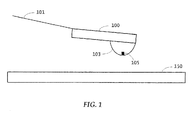
- a slider 100 is shown supported by a suspension 101 in close proximity to a rotating magnetic storage disk 150.
- the slider 100 supports a recording head transducer 103.
- a resistive temperature sensor 105 is shown on the head transducer 103.
- the resistive temperature sensor 105 may be positioned at the close point to the magnetic recording medium 150.
- the close point is generally understood to be the closest point of contact between the head transducer 103 and the magnetic recording medium 150.
- the resistive temperature sensor 105 is preferably configured to sense changes in heat flow for detecting asperities of the medium 150 and head-to-media contact.
- the sensor structure illustrated in Figure 2 includes a first layer 210 comprising a conductive material and having a TCR and a second layer 220 comprising at least one of a specular layer and a seed layer.
- the sensor structure shown in Figure 2 includes the first layer 210 and a second layer 220 comprising a specular layer.
- the sensor structure illustrated in Figure 2 includes the first layer 210 and a second layer 220 comprising a seed layer.
- the conductive material of the first layer 210 preferably comprises Cu, Co, Ni, Ru, Pt, Au, Fe, or Ni X Fe 1-X , or their alloys.
- the first layer 210 preferably has a thickness approximately equal to or less than a mean-free-path of an electron in the conductive material of the first layer 210.
- Figure 3 shows a detailed structure of the resistive temperature sensor 105 shown in Figure 1 in accordance with various embodiments.
- a first layer of the resistive temperature sensor comprises a conducting layer 310 having a conductive material and a TCR.
- a second layer, shown below the conducting layer 310, comprises a specular layer 320.
- the resistive temperature sensor 105 comprises a cap layer 305 above the first layer 310.
- the cap layer preferably comprises Ta, Ru, Cr, NiCr, or NiRu, or their alloys.
- the specular layer 320 is preferably made of metal or oxide thin films.
- the specular layer 320 shown in Figure 3 includes an insulator layer comprising SiO 2 , NiO, Al 2 O 3 , FeOx, HfO 2 , Y 2 O 3 , MgO, TiOx, CuOx, SrTiO 3 , or ZrO.
- the specular layer 320 comprises a metal layer that includes Au, Ag, Cu, Pt, or Ru, or their alloys.
- the specularity factors for Ag, NiFe, Cu, and Ta were found to be approximately 0.8, 0.5, 0.4, and 0, respectively.
- the specular reflection layer 320 confines the electrons in the conducting layer 310 and reduces the surface and interface scattering. The resistance of the conducting layer 310, thus, is reduced.
- the TCR of the resulting thin film resistive temperature sensor 105 therefore, is increased by reducing the total resistance R 0 .
- the specular layer 320 has a preferred specularity of about 0.2 to about 1, with a more preferred specularity of about 0.5 to about 0.8, and a further preferred specularity of about 0.8 to about 1.
- Perfect specular layers 320 provide specularity of 1 and completely eliminate the interface scattering.
- specular layers 320 with specularity of 1 are ideally desirable to provide the largest TCR gain.
- interfacial imperfection and electronic band alignment thwart the realization of specularity of 1.
- a specularity of about 0.5 to about 0.8 is obtainable with careful interface material and electronic band engineering, including in situ high vacuum deposition and/or oxidation.
- the sensor 105 of Figure 1 can further comprise at least one flash metal layer 315 between the first layer 310 and the specular layer 320.
- a flashing of the very thin metal layer 315 between the metallic conducting layer 310 and the specular layer 320 provides for an increase in the specular effect and thus increases the TCR.
- the flash layer 315 preferably comprises Cu, Ag, or Au, or their alloys.
- Figure 4 shows a schematic of a laminated structure of the resistive temperature sensor 105 of Figure 1 comprising a plurality of first conducting layers 410 and a plurality of specular layers 420 adjacent to the conducting layers 410 in accordance with various embodiments.
- Figure 5 shows a schematic of a laminated structure of the resistive temperature sensor 105 of Figure 1 comprising a plurality of the conducting layers 510, a plurality of the specular layers 520 adjacent to the conducting layers 510, and a plurality of flash metal layers 515 between the conducting layers 510 and the specular layers 520 in accordance with other embodiments.
- the individual layer thicknesses are preferably in the range of a few angstroms or a few tens of nanometers.
- the thicknesses of the conducting layers 510 range from about 5 to about 100 nm, with preferred thicknesses ranging from about 5 to about 30 nm.
- the thicknesses of the specular layers 520 range from about 1 to about 20 nm, with preferred thicknesses ranging from about 2 to about 5 nm.
- the thicknesses of the flash metal layers 515 range from about 0.5 to about 5 nm, with preferred thicknesses raging from about 0.5 to about 2 nm.
- the fabrication of the specular reflection layers include sputtering, CVD, MOCVD, IBD, MBE, e-beam evaporation, natural, plasma and reticle oxidation.
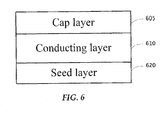
- FIG. 6 another representative structure of the resistive temperature sensor 105 of Figure 1 is shown in Figure 6 .
- the structure in Figure 6 comprises a conducting layer 610 as a first layer, and a seed layer 620 as a second layer.
- the seed layer 620 is shown below the conducting layer 610.
- the seed layer 620 preferably comprises Ta, Ru, Cr, NiCr, or NiRu, or their alloys.
- the resistive temperature sensor 105 illustrated in Figure 6 further comprises a cap layer 605 shown above the conducting layer 610.
- a seeding effect of the seed layer 620 provides for a reduction in the sheet resistance R 0 of the thin film resistive temperature sensor 105 as a means to increase the TCR of the sensor 105.
- the cap layer 605 and the seed layer 620 can (individually or in combination) also provide a specular effect.
- the cap and seed layers 605 and 620 can thus serve as specular layers.
- Figure 7 illustrates various processes for fabricating a resistive temperature sensor in accordance with various embodiments.
- the methodology illustrated in Figure 7 involves forming 710 a head transducer and forming 720, on the head transducer, a first layer comprising a conductive material having a TCR.
- the first layer is formed to a thickness approximately equal to or less than a mean-free-path of an electron in the conductive material of the first layer.
- the conductive material preferably comprises Cu, Co, Ni, Ru, Pt, Au, Fe, or Ni X Fe 1-X , or their alloys.
- the methodology shown in Figure 7 further involves forming 730, on the head transducer, a second layer comprising at least one of a specular layer and a seed layer.
- the methodology illustrated in Figure 7 further involves forming 730, on the head transducer, the second layer comprising a specular layer. In other embodiments, the methodology shown in Figure 7 further involves forming 730, on the head transducer, the second layer comprising a seed layer.
- Figure 8 shows various processes for fabricating a resistive temperature sensor in accordance with other embodiments.
- a head transducer is formed 710, and a first layer comprising a conductive material having a TCR is formed 820 on the formed head transducer.
- the method in Figure 8 further comprises forming 832, on the head transducer, a flash metal layer.
- the flash metal layer preferably comprises a flash material comprising Cu, Ag, or Au, or their alloys.
- the method illustrated in Figure 8 also comprises forming 834 a specular layer such that the flash metal layer is between the first layer and the specular layer.
- the specular layer can comprise SiO 2 , NiO, Al 2 O 3 , FeOx, HfO 2 , Y 2 O 3 , MgO, TiOx, CuOx, SrTiO 3 , or ZrO.
- the specular layer can also comprise Au, Ag, Cu, Pt, or Ru, or their alloys. A flashing of the very thin metal layer between the metallic conducting layer and the specular layer further increases the specular effect of the specular layer and thus increases the TCR of the resistive temperature sensor.
- the method shown in Figure 9 involves forming 915 a seed layer comprising Ta, Ru, Cr, NiCr, or NiRu, or their alloys and forming 920 a first layer on the head transducer.
- the first layer comprises a conducting layer having a conductive material and a TCR.
- the seed layer is formed below the first layer to provide a seeding effect, which reduces the sheet resistance of the thin film sensor as a means to increase the TCR of the sensor.
- the seed and conducting layers are formed in situ in a high vacuum environment, at an elevated temperature relative to room temperature.
- the method in Figure 9 also comprises forming 925 a cap layer over the first layer.
- the cap layer preferably comprises Ta, Ru, Cr, NiCr, or NiRu, or their alloys.
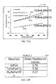
- FIGs 10A and 10B shows TCR data (shown in graphical form 1010 in Figure 10A and data table form 1020 in Figure 10B ) corresponding to a trilayer structure illustrated in Figure 6 .
- the specific trilayer films shown in Figure 10A are a Ni film (30nm) as the conducting layer and Ta (1012) or Ru (1016) or Pt (1018) thin layers (5 nm) as both the specular layers and/or seed layers over and underneath the Ni layer. It is shown that the trilayer metal films show slightly higher TCR than the single layer Ni films (1014).
- the sheet film resistances 1020 of the same films shown in Figure 10 are shown in Table 1 of Figure 10B . It can be seen that the sheet resistances of the trilayer thin films are lower than that of the single layer Ni film.
- the TCR data shown in Figures 11A and 11B corresponds to trilayer films consisting of Ni 96 Fe 4 film (30nm) as the conducting layer and Ta (1112) or Ru (1114) thin films (5 nm) as the specular layers and/or seed layers.
- the sheet resistances of the same films are shown in Table 2 of Figure 11B .
- the trilayer thin films were made in situ in a high vacuum environment (5* 10 -9 torr), which minimized the interfacial impurities between the different layers. TCRs of the trilayer thin films were found to be slightly larger than the single layer films.
- the sheet resistances 1120 shown in Figure 11B of the trilayer thin films were found to be lower than the single layer films.
- an increase in the TCR of a trilayer thin film structure can be achieved by enhancing (e.g., optimizing) the thickness of the seed layer.
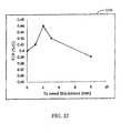
- Figure 12 shows the dependence 1210 of the TCR of the Ni films upon the thickness of the Ta seed layers.
- the total bilayer thickness (Ni + Ta) was maintained at 45nm and the preparation temperature was 250°C.
- An enhanced (e.g., optimized) TCR of ⁇ 0.43%/°C was achieved with a 2nm Ta seed layer. This large TCR represents an approximate 0.43% increase over the TCR of the Ni single layer film prepared at room temperature.
- the TCR of the trilayer film is from about 0.2 to about 0.5 %/°C, with sheet resistance from about 3 to about 8 ohms.
- the optimized seed layer thicknesses are from about 1 to about 5 nm depending upon the seed layer materials and conductive layer materials.
- the optimized seed layer thicknesses are applicable to the trilayer structure where both the underlayer seed and the overlayer (the layer over the conducting layer) utilize the identical thickness.
- the underlayer seed and the overlayer can be used with different thicknesses to provide the specified sheet resistance for device applications. Seed layer thicknesses are subject to optimization to achieve the largest TCR gain.
- processing parameters including deposition rate and process gas flow, are also factors that can be optimized to achieve larger TCR.
- Various fabrication methods are contemplated, including sputtering, other physical vapor deposition processes including thermal evaporation and molecular beam epitaxy, and chemical vapor deposition, for example.
Landscapes
- Engineering & Computer Science (AREA)
- Microelectronics & Electronic Packaging (AREA)
- Physics & Mathematics (AREA)
- Electromagnetism (AREA)
- Chemical & Material Sciences (AREA)
- General Physics & Mathematics (AREA)
- Ceramic Engineering (AREA)
- Chemical Kinetics & Catalysis (AREA)
- Materials Engineering (AREA)
- Mechanical Engineering (AREA)
- Metallurgy (AREA)
- Organic Chemistry (AREA)
- Manufacturing & Machinery (AREA)
- Magnetic Heads (AREA)
- Measuring Temperature Or Quantity Of Heat (AREA)
- Adjustment Of The Magnetic Head Position Track Following On Tapes (AREA)
- Chemical Vapour Deposition (AREA)
- Hall/Mr Elements (AREA)
- Thermistors And Varistors (AREA)
Abstract
Description
- Embodiments of the disclosure are directed to apparatuses comprising a head transducer and a resistive temperature sensor provided on the head transducer. Embodiments of the disclosure are directed to fabricating a resistive temperature sensor, such as a resistive temperature sensor for use on a head transducer. Embodiments are directed to methods and apparatuses for fabricating a resistive temperature sensor with a large temperature coefficient resistance (TCR).
- According to various embodiments, apparatuses of the disclosure comprise a head transducer and a resistive temperature sensor provided on the head transducer. The resistive temperature sensor comprises a first layer comprising a conductive material and having a TCR and a second layer comprising at least one of a specular layer and a seed layer. According to some embodiments, the first layer has a thickness approximately equal to or less than a mean-free-path of an electron in the conductive material of the first layer.
- In accordance with other embodiments, methods for fabricating a resistive temperature sensor includes forming, on a head transducer, a first layer comprising a conductive material having a TCR and forming, on the head transducer, a second layer comprising at least one of a specular layer and a seed layer. According to some embodiments, forming the first layer comprises forming the first layer to a thickness approximately equal to or less than a mean-free-path of an electron in the conductive material of the first layer.
- These and other features and aspects which characterize various embodiments can be understood in view of the following detailed discussion and the accompanying drawings.
- Embodiments of the present invention will now be described by way of further example only and with reference to the accompanying drawings, in which:
-
Figure 1 shows a simplified side view of a head transducer arrangement which incorporates a resistive temperature sensor in accordance with various embodiments; -
Figure 2 shows a structure of a resistive temperature sensor in accordance with various embodiments; -
Figures 3-6 show structures of a resistive temperature sensor in accordance with other embodiments; -
Figure 7 illustrates various processes for fabricating a resistive temperature sensor in accordance with various embodiments; -
Figures 8-9 illustrate various processes for fabricating a resistive temperature sensor in accordance with other embodiments; -
Figures 10A and 10B illustrate TCR data corresponding to trilayer films consisting of an Ni film as a conducting layer, and Ta, Ru or Pt thin films as specular layers or seed layers both over and underneath the Ni layer in accordance with various embodiments; -
Figures 11A and 11B illustrate TCR data corresponding to trilayer films consisting of Ni96Fe4 film as a conducting layer, and Ta or Ru thin films as specular layers or seed layers both over and underneath the NiFe layer in accordance with various embodiments; and -
Figure 12 shows dependence of the TCR of Ni films upon the thickness of Ta seed layers in accordance with various embodiments. - Metal thin films with a sufficient temperature coefficient of resistance can be used as temperature sensors. In particular, metal thin films with a sufficiently high TCR can be used to fabricate temperature sensors for detecting head-media contact and thermal asperities in hard disk drives and other magnetic recording devices. The signal noise ratio (SNR) associated with contact detection (CD) and thermal asperity (TA) detection is dependent upon the TCR of the materials used to fabricate CD and/or TA detection sensors.
- To obtain a sufficiently high SNR, materials with larger TCR are generally desirable. A typical CD or TA detection sensor consists of metal thin films having thicknesses of a few tens of nanometers. In such typical detection sensors, the mean-free-path of the electrons is nearly equal to or greater than the thicknesses of the films. The TCRs of the thin film materials can, therefore, be much less than the bulk TCRs of the same materials due to excessive surface and interface scatterings. Deliberately designed materials and the fabricating methods are, thus, needed to achieve the desirable large TCRs.
- Embodiments of the disclosure are directed to laminated metal and metal/oxide thin films and methods of fabricating same to achieve a large TCR for temperature sensing applications. Laminated thin film structures, according to various embodiments, preferably comprise a conductive metal layer and another layer which can either be a metal specular layer, an oxide specular layer, or a seed layer. The conductive metal layer has a TCR. The thicknesses of various layers in the laminated thin film structure are preferably in the range of few to a few tens of nanometers. Various embodiments directed to combinations of deliberately optimized multilayer thin film structures and fabrication methods of such films at elevated temperatures are disclosed herein to obtain the large TCR.
- The TCR of a given material is defined by the following formula:

- Here, R0 is the resistance at the room temperature and dR/dt denotes the resistance change as a function of the temperature. Given that the TCR is inversely proportional to R0, a reduction in R0 is expected to yield a larger TCR. Likewise, an increase in dR/dt leads to a larger TCR as well.
- R0 accounts for resistances impacted by many factors. For example, surface and interface scattering, together with structural and chemical defect scattering, add to the material resistance, R0, while contributing very little to the TCR. Since dR/dt is the thermally activated resistance of the material and is in large part an intrinsic characteristic of the material, embodiments of the disclosure target the reduction of R0 of the thin films to increase the TCR of temperature sensing devices, such as CD and TA detection sensors.
- In accordance with various embodiments, and with reference to
Figure 1 , aslider 100 is shown supported by asuspension 101 in close proximity to a rotatingmagnetic storage disk 150. Theslider 100 supports arecording head transducer 103. Aresistive temperature sensor 105 is shown on thehead transducer 103. Theresistive temperature sensor 105 may be positioned at the close point to themagnetic recording medium 150. The close point is generally understood to be the closest point of contact between thehead transducer 103 and themagnetic recording medium 150. Theresistive temperature sensor 105 is preferably configured to sense changes in heat flow for detecting asperities of themedium 150 and head-to-media contact. - Referring to
Figure 2 , a structure of theresistive temperature sensor 105 shown inFigure 1 is illustrated in accordance with various embodiments. The sensor structure illustrated inFigure 2 includes afirst layer 210 comprising a conductive material and having a TCR and asecond layer 220 comprising at least one of a specular layer and a seed layer. In some embodiments, the sensor structure shown inFigure 2 includes thefirst layer 210 and asecond layer 220 comprising a specular layer. In other embodiments, the sensor structure illustrated inFigure 2 includes thefirst layer 210 and asecond layer 220 comprising a seed layer. The conductive material of thefirst layer 210 preferably comprises Cu, Co, Ni, Ru, Pt, Au, Fe, or NiXFe1-X, or their alloys. Thefirst layer 210 preferably has a thickness approximately equal to or less than a mean-free-path of an electron in the conductive material of thefirst layer 210. -
Figure 3 shows a detailed structure of theresistive temperature sensor 105 shown inFigure 1 in accordance with various embodiments. According to embodiments consistent withFigure 3 , a first layer of the resistive temperature sensor comprises a conductinglayer 310 having a conductive material and a TCR. A second layer, shown below theconducting layer 310, comprises aspecular layer 320. Theresistive temperature sensor 105 comprises acap layer 305 above thefirst layer 310. - The cap layer preferably comprises Ta, Ru, Cr, NiCr, or NiRu, or their alloys. The
specular layer 320 is preferably made of metal or oxide thin films. In one representative embodiment, thespecular layer 320 shown inFigure 3 includes an insulator layer comprising SiO2, NiO, Al2O3, FeOx, HfO2, Y2O3, MgO, TiOx, CuOx, SrTiO3, or ZrO. In another representative embodiment, thespecular layer 320 comprises a metal layer that includes Au, Ag, Cu, Pt, or Ru, or their alloys. - Specular effects have been observed and measured in many cases by the inventors. For example, using SiO2 and NiO as the
specular layer 320 inFigure 3 , the specularity factors for Ag, NiFe, Cu, and Ta were found to be approximately 0.8, 0.5, 0.4, and 0, respectively. Thespecular reflection layer 320 confines the electrons in the conductinglayer 310 and reduces the surface and interface scattering. The resistance of theconducting layer 310, thus, is reduced. The TCR of the resulting thin filmresistive temperature sensor 105, therefore, is increased by reducing the total resistance R0. Thespecular layer 320 has a preferred specularity of about 0.2 to about 1, with a more preferred specularity of about 0.5 to about 0.8, and a further preferred specularity of about 0.8 to about 1. Perfectspecular layers 320 provide specularity of 1 and completely eliminate the interface scattering. Thus,specular layers 320 with specularity of 1 are ideally desirable to provide the largest TCR gain. However, interfacial imperfection and electronic band alignment thwart the realization of specularity of 1. In practice, a specularity of about 0.5 to about 0.8 is obtainable with careful interface material and electronic band engineering, including in situ high vacuum deposition and/or oxidation. - As illustrated in
Figure 3 , thesensor 105 ofFigure 1 can further comprise at least oneflash metal layer 315 between thefirst layer 310 and thespecular layer 320. A flashing of the verythin metal layer 315 between themetallic conducting layer 310 and thespecular layer 320 provides for an increase in the specular effect and thus increases the TCR. Theflash layer 315 preferably comprises Cu, Ag, or Au, or their alloys. -
Figure 4 shows a schematic of a laminated structure of theresistive temperature sensor 105 ofFigure 1 comprising a plurality of first conducting layers 410 and a plurality ofspecular layers 420 adjacent to the conductinglayers 410 in accordance with various embodiments.Figure 5 shows a schematic of a laminated structure of theresistive temperature sensor 105 ofFigure 1 comprising a plurality of the conductinglayers 510, a plurality of thespecular layers 520 adjacent to the conducting layers 510, and a plurality offlash metal layers 515 between the conductinglayers 510 and thespecular layers 520 in accordance with other embodiments. The individual layer thicknesses are preferably in the range of a few angstroms or a few tens of nanometers. The thicknesses of the conductinglayers 510 range from about 5 to about 100 nm, with preferred thicknesses ranging from about 5 to about 30 nm. The thicknesses of thespecular layers 520 range from about 1 to about 20 nm, with preferred thicknesses ranging from about 2 to about 5 nm. The thicknesses of theflash metal layers 515 range from about 0.5 to about 5 nm, with preferred thicknesses raging from about 0.5 to about 2 nm. The fabrication of the specular reflection layers include sputtering, CVD, MOCVD, IBD, MBE, e-beam evaporation, natural, plasma and reticle oxidation. - According to various embodiments, another representative structure of the
resistive temperature sensor 105 ofFigure 1 is shown inFigure 6 . The structure inFigure 6 comprises aconducting layer 610 as a first layer, and aseed layer 620 as a second layer. Theseed layer 620 is shown below theconducting layer 610. Theseed layer 620 preferably comprises Ta, Ru, Cr, NiCr, or NiRu, or their alloys. Theresistive temperature sensor 105 illustrated inFigure 6 further comprises acap layer 605 shown above theconducting layer 610. A seeding effect of theseed layer 620 provides for a reduction in the sheet resistance R0 of the thin filmresistive temperature sensor 105 as a means to increase the TCR of thesensor 105. Based on the same structure shown inFigure 6 , thecap layer 605 and theseed layer 620 can (individually or in combination) also provide a specular effect. The cap andseed layers -
Figure 7 illustrates various processes for fabricating a resistive temperature sensor in accordance with various embodiments. The methodology illustrated inFigure 7 involves forming 710 a head transducer and forming 720, on the head transducer, a first layer comprising a conductive material having a TCR. The first layer is formed to a thickness approximately equal to or less than a mean-free-path of an electron in the conductive material of the first layer. The conductive material preferably comprises Cu, Co, Ni, Ru, Pt, Au, Fe, or NiXFe1-X, or their alloys. The methodology shown inFigure 7 further involves forming 730, on the head transducer, a second layer comprising at least one of a specular layer and a seed layer. In some embodiments, the methodology illustrated inFigure 7 further involves forming 730, on the head transducer, the second layer comprising a specular layer. In other embodiments, the methodology shown inFigure 7 further involves forming 730, on the head transducer, the second layer comprising a seed layer. -
Figure 8 shows various processes for fabricating a resistive temperature sensor in accordance with other embodiments. According to the embodiment shown inFigure 8 , a head transducer is formed 710, and a first layer comprising a conductive material having a TCR is formed 820 on the formed head transducer. The method inFigure 8 further comprises forming 832, on the head transducer, a flash metal layer. The flash metal layer preferably comprises a flash material comprising Cu, Ag, or Au, or their alloys. The method illustrated inFigure 8 also comprises forming 834 a specular layer such that the flash metal layer is between the first layer and the specular layer. The specular layer can comprise SiO2, NiO, Al2O3, FeOx, HfO2, Y2O3, MgO, TiOx, CuOx, SrTiO3, or ZrO. The specular layer can also comprise Au, Ag, Cu, Pt, or Ru, or their alloys. A flashing of the very thin metal layer between the metallic conducting layer and the specular layer further increases the specular effect of the specular layer and thus increases the TCR of the resistive temperature sensor. - Referring to
Figure 9 , there is illustrated various processes for fabricating a resistive temperature sensor in accordance with various embodiments. After forming 710 a head transducer, the method shown inFigure 9 involves forming 915 a seed layer comprising Ta, Ru, Cr, NiCr, or NiRu, or their alloys and forming 920 a first layer on the head transducer. The first layer comprises a conducting layer having a conductive material and a TCR. The seed layer is formed below the first layer to provide a seeding effect, which reduces the sheet resistance of the thin film sensor as a means to increase the TCR of the sensor. The seed and conducting layers are formed in situ in a high vacuum environment, at an elevated temperature relative to room temperature. The method inFigure 9 also comprises forming 925 a cap layer over the first layer. The cap layer preferably comprises Ta, Ru, Cr, NiCr, or NiRu, or their alloys. -
Figures 10A and 10B shows TCR data (shown ingraphical form 1010 inFigure 10A anddata table form 1020 inFigure 10B ) corresponding to a trilayer structure illustrated inFigure 6 . The specific trilayer films shown inFigure 10A are a Ni film (30nm) as the conducting layer and Ta (1012) or Ru (1016) or Pt (1018) thin layers (5 nm) as both the specular layers and/or seed layers over and underneath the Ni layer. It is shown that the trilayer metal films show slightly higher TCR than the single layer Ni films (1014). Thesheet film resistances 1020 of the same films shown inFigure 10 are shown in Table 1 ofFigure 10B . It can be seen that the sheet resistances of the trilayer thin films are lower than that of the single layer Ni film. - The TCR data shown in
Figures 11A and 11B (shown ingraphical form 1110 inFigure 11A anddata table form 1120 inFigure 11B ) corresponds to trilayer films consisting of Ni96Fe4 film (30nm) as the conducting layer and Ta (1112) or Ru (1114) thin films (5 nm) as the specular layers and/or seed layers. The sheet resistances of the same films are shown in Table 2 ofFigure 11B . The trilayer thin films were made in situ in a high vacuum environment (5* 10-9 torr), which minimized the interfacial impurities between the different layers. TCRs of the trilayer thin films were found to be slightly larger than the single layer films. In addition, thesheet resistances 1120 shown inFigure 11B of the trilayer thin films were found to be lower than the single layer films. - Fabrication of the multi-layer thin film structures at elevated temperatures as compared to room temperature results in larger grain size of the thin film materials, and thus a reduction in the residual resistance resulting from defect scattering. The reduction in R0 is expected to enhance the TCR. Preparation of the 5nm Ta/30nm Ni/5nm Ta trilayer thin films fabricated at 250°C and 350°C yielded a TCR of ∼0.38%/°C, which compares to a TCR of ∼0.32%/°C observed in the same trilayer thin films prepared at room temperature.
- In addition, an increase in the TCR of a trilayer thin film structure can be achieved by enhancing (e.g., optimizing) the thickness of the seed layer.
Figure 12 shows thedependence 1210 of the TCR of the Ni films upon the thickness of the Ta seed layers. The total bilayer thickness (Ni + Ta) was maintained at 45nm and the preparation temperature was 250°C. An enhanced (e.g., optimized) TCR of ∼0.43%/°C was achieved with a 2nm Ta seed layer. This large TCR represents an approximate 0.43% increase over the TCR of the Ni single layer film prepared at room temperature. - Depending on the materials of the conductive layers and total thickness, the TCR of the trilayer film is from about 0.2 to about 0.5 %/°C, with sheet resistance from about 3 to about 8 ohms. The optimized seed layer thicknesses are from about 1 to about 5 nm depending upon the seed layer materials and conductive layer materials. The optimized seed layer thicknesses are applicable to the trilayer structure where both the underlayer seed and the overlayer (the layer over the conducting layer) utilize the identical thickness. Furthermore, the underlayer seed and the overlayer can be used with different thicknesses to provide the specified sheet resistance for device applications. Seed layer thicknesses are subject to optimization to achieve the largest TCR gain.
- Other processing parameters, including deposition rate and process gas flow, are also factors that can be optimized to achieve larger TCR. Various fabrication methods are contemplated, including sputtering, other physical vapor deposition processes including thermal evaporation and molecular beam epitaxy, and chemical vapor deposition, for example.
- It is to be understood that even though numerous characteristics and advantages of various embodiments disclosed herein have been set forth in the foregoing description, together with details of the structure and function of various embodiments, this detailed description is illustrative only, and changes may be made in detail, especially in matters of structure and arrangements of parts within the principles of the presently disclosed subject matter to the full extent indicated by the broad general meaning of the terms in which the appended claims are expressed.
Claims (25)
- An apparatus, comprising:a head transducer (103); anda resistive temperature sensor (105) provided on the head transducer, the sensor comprising:a first layer (210) comprising a conductive material and having a temperature coefficient of resistance; anda second layer (220) comprising at least one of a specular layer and a seed layer.
- The apparatus of claim 1, wherein the conductive material comprises Cu, Co, Ni, Ru, Pt, Au, Fe, or NiXFe1-X, or their alloys.
- The apparatus of claim 1 or claim 2, wherein the sensor comprises a cap layer (305) on the first layer (310), the cap layer comprising Ta, Ru, Cr, NiCr, or NiRu, or their alloys.
- The apparatus of any one of the preceding claims, wherein the first layer (210) has a thickness approximately equal to or less than a mean-free-path of an electron in the conductive material of the first layer.
- The apparatus of any one of the preceding claims, wherein the second layer comprises the specular layer (320).
- The apparatus of claim 5, wherein the specular layer comprises an insulator layer.
- The apparatus of claim 6, wherein the insulator layer comprises SiO2, NiO, Al2O3, FeOX, HfO2, Y2O3, MgO, TiOx, CuOx, SrTiO3, or ZrO.
- The apparatus of claim 5, wherein the specular layer comprises a metal layer.
- The apparatus of claim 8, wherein the metal layer comprises Au, Ag, Cu, Pt, or Ru, or their alloys.
- The apparatus of any one of claims 5 to 9, further comprising at least one flash metal layer (315) between the first layer and the specular layer.
- The apparatus of claim 10, wherein the flash layer comprises Cu, Ag, or Au, or their alloys.
- The apparatus of any one of claims 5 to 11, wherein the sensor comprises a plurality of the first layers (410) and a plurality of the specular layers (420).
- The apparatus of any one of claims 5 to 12, wherein the specular layer has a specularity of about 0.2 to about 0.8.
- The apparatus of any one of claims 1 to 4, wherein the second layer comprises the seed layer.
- The apparatus of claim 14, wherein the seed layer comprises Ta, Ru, Cr, NiCr, or NiRu, or their alloys.
- A method of fabricating a resistive temperature sensor (105), comprising:forming, on a head transducer (103), a first layer (210) comprising a conductive material having a temperature coefficient of resistance; andforming, on the head transducer, a second layer (220) comprising at least one of a specular layer and a seed layer.
- The method of claim 16, wherein forming the first layer (210) comprises forming the first layer to a thickness approximately equal to or less than a mean-free-path of an electron in the conductive material of the first layer.
- The method of claim 16 or claim 17, wherein the conductive material comprises Cu, Co, Ni, Ru, Pt, Au, Fe, or NiXFe1-X, or their alloys.
- The method of any one of claims 16 to 18, comprising forming a cap layer (305) over the first layer (310), the cap layer comprising Ta, Ru, Cr, NiCr, or NiRu, or their alloys.
- The method of any one of claims 16 to 19, wherein forming the second layer comprises forming the specular layer (320) comprising SiO2, NiO, Al2O3, FeOX, HfO2, Y2O3, MgO, TiOX, CuOX, SrTiO3, or ZrO.
- The method of any one of claims 16 to 19, wherein forming the second layer comprises forming the specular layer (320) comprising Au, Ag, Cu, Pt, or Ru, or their alloys.
- The method of any one of claims 16 to 21, comprising forming a flash metal layer (315) between the first layer and the second layer, wherein:forming the second layer comprises forming the specular layer (320); andforming the flash metal layer (315) comprises forming a flash material comprising Cu, Ag, or Au, or their alloys.
- The method of any one of claims 16 to 20, wherein forming the second layer comprises forming the seed layer comprising Ta, Ru, Cr, NiCr, or NiRu, or their alloys.
- The method of any one of claims 16 to 20 and 23, wherein:forming the second layer comprises forming the seed layer; andforming the seed and conducting layers is performed in situ in a high vacuum environment.
- The method of any one of claims 16 to 20 and 23, wherein:forming the second layer comprises forming the seed layer; andforming the seed and conducting layers is performed at an elevated temperature relative to room temperature.
Applications Claiming Priority (1)
| Application Number | Priority Date | Filing Date | Title |
|---|---|---|---|
| US13/687,445 US9664572B2 (en) | 2012-11-28 | 2012-11-28 | Thin films having large temperature coefficient of resistance and methods of fabricating same |
Publications (2)
| Publication Number | Publication Date |
|---|---|
| EP2738777A2 true EP2738777A2 (en) | 2014-06-04 |
| EP2738777A3 EP2738777A3 (en) | 2014-09-10 |
Family
ID=49766858
Family Applications (1)
| Application Number | Title | Priority Date | Filing Date |
|---|---|---|---|
| EP13194710.3A Withdrawn EP2738777A3 (en) | 2012-11-28 | 2013-11-27 | Thin films having large temperature coefficient of resistance and methods of fabricating same |
Country Status (5)
| Country | Link |
|---|---|
| US (1) | US9664572B2 (en) |
| EP (1) | EP2738777A3 (en) |
| JP (1) | JP6061835B2 (en) |
| KR (1) | KR101659615B1 (en) |
| CN (1) | CN103852184B (en) |
Families Citing this family (3)
| Publication number | Priority date | Publication date | Assignee | Title |
|---|---|---|---|---|
| KR102325458B1 (en) * | 2015-05-27 | 2021-11-16 | 생-고뱅 퍼포먼스 플라스틱스 코포레이션 | A biosensor electrode and a method for forming the same |
| WO2019168655A1 (en) * | 2018-02-28 | 2019-09-06 | Applied Materials, Inc. | Method for measuring a temperature |
| RU2756800C1 (en) * | 2020-12-08 | 2021-10-05 | Федеральное государственное автономное образовательное учреждение высшего образования "Национальный исследовательский технологический университет "МИСиС" | Superconducting resistance thermometer |
Family Cites Families (18)
| Publication number | Priority date | Publication date | Assignee | Title |
|---|---|---|---|---|
| US4454495A (en) * | 1982-08-31 | 1984-06-12 | The United States Of America As Represented By The United States Department Of Energy | Layered ultra-thin coherent structures used as electrical resistors having low temperature coefficient of resistivity |
| US4952904A (en) * | 1988-12-23 | 1990-08-28 | Honeywell Inc. | Adhesion layer for platinum based sensors |
| JPH06295404A (en) | 1993-04-09 | 1994-10-21 | Matsushita Electric Ind Co Ltd | Magnetic recording / reproducing device |
| BE1005586A0 (en) | 1993-05-10 | 1993-11-09 | Philips Electronics Nv | Recording device WITH A TEMPERATURE-DEPENDENT WRITE CURRENT REGULATIONS. |
| JPH0817156A (en) | 1994-06-30 | 1996-01-19 | Toshiba Corp | Data recording / reproducing apparatus and disc inspection method thereof |
| US6556390B1 (en) * | 1999-10-28 | 2003-04-29 | Seagate Technology Llc | Spin valve sensors with an oxide layer utilizing electron specular scattering effect |
| JP3600538B2 (en) | 2001-03-15 | 2004-12-15 | アルプス電気株式会社 | Magnetic sensing element and method of manufacturing the same |
| US6735060B2 (en) | 2001-06-20 | 2004-05-11 | International Business Machines Corporation | Spin valve sensor with a metal and metal oxide cap layer structure |
| JP2003123204A (en) | 2001-10-04 | 2003-04-25 | Hitachi Ltd | Magnetic disk drive |
| US7833800B2 (en) | 2002-04-01 | 2010-11-16 | Palo Alto Research Center Incorporated | Thermal sensing with bridge circuitry |
| US6950279B2 (en) * | 2003-01-30 | 2005-09-27 | Headway Technologies, Inc. | Thin-film magnetic head with thin-film coil of low resistance |
| JP2006024289A (en) * | 2004-07-08 | 2006-01-26 | Tdk Corp | Thin film magnetic head with heating element, head gimbal assembly with thin film magnetic head, magnetic disk unit with head gimbal assembly |
| JP4102371B2 (en) | 2005-02-17 | 2008-06-18 | Tdk株式会社 | Thin film magnetic head |
| JP2007026591A (en) * | 2005-07-20 | 2007-02-01 | Alps Electric Co Ltd | Thin-film magnetic head |
| US7986027B2 (en) * | 2006-10-20 | 2011-07-26 | Analog Devices, Inc. | Encapsulated metal resistor |
| US8351157B2 (en) | 2010-07-06 | 2013-01-08 | Tdk Corporation | Thin film magnetic head having temperature detection mechanism, head gimbals assembly, head arm assembly and magnetic disk device |
| US8817406B2 (en) * | 2011-12-30 | 2014-08-26 | HGST Netherlands B.V. | Magnetic-recording head with touch-down detector incorporating a carbon nano-tube |
| US8765273B1 (en) * | 2012-08-21 | 2014-07-01 | Seagate Technology Llc | Tuned heatsink layers |
-
2012
- 2012-11-28 US US13/687,445 patent/US9664572B2/en active Active
-
2013
- 2013-11-27 KR KR1020130145510A patent/KR101659615B1/en not_active Expired - Fee Related
- 2013-11-27 JP JP2013244830A patent/JP6061835B2/en not_active Expired - Fee Related
- 2013-11-27 EP EP13194710.3A patent/EP2738777A3/en not_active Withdrawn
- 2013-11-27 CN CN201310613275.8A patent/CN103852184B/en not_active Expired - Fee Related
Non-Patent Citations (1)
| Title |
|---|
| None |
Also Published As
| Publication number | Publication date |
|---|---|
| KR101659615B1 (en) | 2016-09-23 |
| US9664572B2 (en) | 2017-05-30 |
| CN103852184B (en) | 2018-04-24 |
| JP2014107007A (en) | 2014-06-09 |
| KR20140068778A (en) | 2014-06-09 |
| JP6061835B2 (en) | 2017-01-18 |
| EP2738777A3 (en) | 2014-09-10 |
| US20140146856A1 (en) | 2014-05-29 |
| CN103852184A (en) | 2014-06-11 |
Similar Documents
| Publication | Publication Date | Title |
|---|---|---|
| CN105009211B (en) | Articles including intermediate layers and methods of forming | |
| US7307818B1 (en) | Method and system for providing a stable spin filter | |
| US20080253038A1 (en) | Tunneling magnetic sensor including free magnetic layer and magnesium protective layer disposed thereon and method for manufacturing tunneling magnetoresistive sensor | |
| EP1903623A2 (en) | Tunnel type magnetic sensor having fixed magnetic layer of composite structure containing CoFeB film and method for manufacturing the same | |
| US7898776B2 (en) | Tunneling magnetic sensing element including enhancing layer having high Fe concentration in the vicinity of barrier layer | |
| US20090258253A1 (en) | Magnetic recording medium for high density recording and magnetic storage device using same | |
| US20080151438A1 (en) | Magnetoresistive element | |
| CN117694031A (en) | Novel doping process to refine grain size for smoother BiSb film surface | |
| CN101499515A (en) | Magnetoresistive element and method of manufacturing the same | |
| US6632474B1 (en) | Robust hard bias/conductor lead structures for future GMR heads | |
| US9664572B2 (en) | Thin films having large temperature coefficient of resistance and methods of fabricating same | |
| US6630255B1 (en) | Multilayer perpendicular magnetic recording media with exchange decoupled spacer layers | |
| US6607641B2 (en) | Method of producing exchange coupling film and method of producing magnetoresistive sensor by using the exchange coupling film | |
| US7643254B2 (en) | Tunnel-effect type magnetic sensor having free layer including non-magnetic metal layer | |
| US7961442B2 (en) | Tunneling magnetic detecting element having insulation barrier layer and method for making the same | |
| US7738218B2 (en) | Magnetic detection head and method for manufacturing the same | |
| US8130476B2 (en) | Tunneling magnetic sensing element and method for manufacturing the same | |
| US6652906B1 (en) | Fabrication of a magnetoresistance sensor structure having a spacer layer produced by multiple deposition and oxidation steps | |
| US20080186638A1 (en) | Tunneling magnetic sensing element having free magnetic layer inserted with nonmagnetic metal layers | |
| JPWO2004051629A1 (en) | Magnetic disk drive and manufacturing method thereof | |
| US7969690B2 (en) | Tunneling magnetoresistive element which includes Mg-O barrier layer and in which nonmagnetic metal sublayer is disposed in one of magnetic layers | |
| US7916436B2 (en) | Tunneling magnetic sensor including platinum layer and method for producing the same | |
| JP2006128410A (en) | Magnetic detecting element and its manufacturing method | |
| US20080055786A1 (en) | Tunnel type magnetic sensor having protective layer formed from Pt or Ru on free magnetic layer, and method for manufacturing the same | |
| JP2008034784A (en) | Tunnel-type magnetic detection element and method of manufacturing the same |
Legal Events
| Date | Code | Title | Description |
|---|---|---|---|
| PUAI | Public reference made under article 153(3) epc to a published international application that has entered the european phase |
Free format text: ORIGINAL CODE: 0009012 |
|
| 17P | Request for examination filed |
Effective date: 20131127 |
|
| AK | Designated contracting states |
Kind code of ref document: A2 Designated state(s): AL AT BE BG CH CY CZ DE DK EE ES FI FR GB GR HR HU IE IS IT LI LT LU LV MC MK MT NL NO PL PT RO RS SE SI SK SM TR |
|
| AX | Request for extension of the european patent |
Extension state: BA ME |
|
| PUAL | Search report despatched |
Free format text: ORIGINAL CODE: 0009013 |
|
| AK | Designated contracting states |
Kind code of ref document: A3 Designated state(s): AL AT BE BG CH CY CZ DE DK EE ES FI FR GB GR HR HU IE IS IT LI LT LU LV MC MK MT NL NO PL PT RO RS SE SI SK SM TR |
|
| AX | Request for extension of the european patent |
Extension state: BA ME |
|
| RIC1 | Information provided on ipc code assigned before grant |
Ipc: G11B 5/60 20060101ALI20140804BHEP Ipc: G01K 7/16 20060101ALI20140804BHEP Ipc: H01C 7/02 20060101AFI20140804BHEP Ipc: H01C 7/00 20060101ALI20140804BHEP |
|
| STAA | Information on the status of an ep patent application or granted ep patent |
Free format text: STATUS: THE APPLICATION IS DEEMED TO BE WITHDRAWN |
|
| 18D | Application deemed to be withdrawn |
Effective date: 20150311 |