EP2738604A1 - Photoresist employing photodimerization chemistry and method for manufacturing organic light emitting diode display using the same - Google Patents
Photoresist employing photodimerization chemistry and method for manufacturing organic light emitting diode display using the same Download PDFInfo
- Publication number
- EP2738604A1 EP2738604A1 EP13171836.3A EP13171836A EP2738604A1 EP 2738604 A1 EP2738604 A1 EP 2738604A1 EP 13171836 A EP13171836 A EP 13171836A EP 2738604 A1 EP2738604 A1 EP 2738604A1
- Authority
- EP
- European Patent Office
- Prior art keywords
- photoresist
- light emitting
- organic light
- monomer
- emitting diode
- Prior art date
- Legal status (The legal status is an assumption and is not a legal conclusion. Google has not performed a legal analysis and makes no representation as to the accuracy of the status listed.)
- Granted
Links
Images


Classifications
-
- C—CHEMISTRY; METALLURGY
- C08—ORGANIC MACROMOLECULAR COMPOUNDS; THEIR PREPARATION OR CHEMICAL WORKING-UP; COMPOSITIONS BASED THEREON
- C08F—MACROMOLECULAR COMPOUNDS OBTAINED BY REACTIONS ONLY INVOLVING CARBON-TO-CARBON UNSATURATED BONDS
- C08F220/00—Copolymers of compounds having one or more unsaturated aliphatic radicals, each having only one carbon-to-carbon double bond, and only one being terminated by only one carboxyl radical or a salt, anhydride ester, amide, imide or nitrile thereof
- C08F220/02—Monocarboxylic acids having less than ten carbon atoms; Derivatives thereof
- C08F220/10—Esters
- C08F220/22—Esters containing halogen
- C08F220/24—Esters containing halogen containing perhaloalkyl radicals
-
- C—CHEMISTRY; METALLURGY
- C08—ORGANIC MACROMOLECULAR COMPOUNDS; THEIR PREPARATION OR CHEMICAL WORKING-UP; COMPOSITIONS BASED THEREON
- C08F—MACROMOLECULAR COMPOUNDS OBTAINED BY REACTIONS ONLY INVOLVING CARBON-TO-CARBON UNSATURATED BONDS
- C08F20/00—Homopolymers and copolymers of compounds having one or more unsaturated aliphatic radicals, each having only one carbon-to-carbon double bond, and only one being terminated by only one carboxyl radical or a salt, anhydride, ester, amide, imide or nitrile thereof
- C08F20/02—Monocarboxylic acids having less than ten carbon atoms, Derivatives thereof
- C08F20/10—Esters
-
- C—CHEMISTRY; METALLURGY
- C08—ORGANIC MACROMOLECULAR COMPOUNDS; THEIR PREPARATION OR CHEMICAL WORKING-UP; COMPOSITIONS BASED THEREON
- C08F—MACROMOLECULAR COMPOUNDS OBTAINED BY REACTIONS ONLY INVOLVING CARBON-TO-CARBON UNSATURATED BONDS
- C08F20/00—Homopolymers and copolymers of compounds having one or more unsaturated aliphatic radicals, each having only one carbon-to-carbon double bond, and only one being terminated by only one carboxyl radical or a salt, anhydride, ester, amide, imide or nitrile thereof
- C08F20/02—Monocarboxylic acids having less than ten carbon atoms, Derivatives thereof
- C08F20/10—Esters
- C08F20/22—Esters containing halogen
- C08F20/24—Esters containing halogen containing perhaloalkyl radicals
-
- C—CHEMISTRY; METALLURGY
- C08—ORGANIC MACROMOLECULAR COMPOUNDS; THEIR PREPARATION OR CHEMICAL WORKING-UP; COMPOSITIONS BASED THEREON
- C08F—MACROMOLECULAR COMPOUNDS OBTAINED BY REACTIONS ONLY INVOLVING CARBON-TO-CARBON UNSATURATED BONDS
- C08F220/00—Copolymers of compounds having one or more unsaturated aliphatic radicals, each having only one carbon-to-carbon double bond, and only one being terminated by only one carboxyl radical or a salt, anhydride ester, amide, imide or nitrile thereof
- C08F220/02—Monocarboxylic acids having less than ten carbon atoms; Derivatives thereof
- C08F220/10—Esters
- C08F220/12—Esters of monohydric alcohols or phenols
- C08F220/16—Esters of monohydric alcohols or phenols of phenols or of alcohols containing two or more carbon atoms
- C08F220/18—Esters of monohydric alcohols or phenols of phenols or of alcohols containing two or more carbon atoms with acrylic or methacrylic acids
- C08F220/1818—C13or longer chain (meth)acrylate, e.g. stearyl (meth)acrylate
-
- G—PHYSICS
- G03—PHOTOGRAPHY; CINEMATOGRAPHY; ANALOGOUS TECHNIQUES USING WAVES OTHER THAN OPTICAL WAVES; ELECTROGRAPHY; HOLOGRAPHY
- G03F—PHOTOMECHANICAL PRODUCTION OF TEXTURED OR PATTERNED SURFACES, e.g. FOR PRINTING, FOR PROCESSING OF SEMICONDUCTOR DEVICES; MATERIALS THEREFOR; ORIGINALS THEREFOR; APPARATUS SPECIALLY ADAPTED THEREFOR
- G03F7/00—Photomechanical, e.g. photolithographic, production of textured or patterned surfaces, e.g. printing surfaces; Materials therefor, e.g. comprising photoresists; Apparatus specially adapted therefor
- G03F7/004—Photosensitive materials
- G03F7/0045—Photosensitive materials with organic non-macromolecular light-sensitive compounds not otherwise provided for, e.g. dissolution inhibitors
-
- G—PHYSICS
- G03—PHOTOGRAPHY; CINEMATOGRAPHY; ANALOGOUS TECHNIQUES USING WAVES OTHER THAN OPTICAL WAVES; ELECTROGRAPHY; HOLOGRAPHY
- G03F—PHOTOMECHANICAL PRODUCTION OF TEXTURED OR PATTERNED SURFACES, e.g. FOR PRINTING, FOR PROCESSING OF SEMICONDUCTOR DEVICES; MATERIALS THEREFOR; ORIGINALS THEREFOR; APPARATUS SPECIALLY ADAPTED THEREFOR
- G03F7/00—Photomechanical, e.g. photolithographic, production of textured or patterned surfaces, e.g. printing surfaces; Materials therefor, e.g. comprising photoresists; Apparatus specially adapted therefor
- G03F7/004—Photosensitive materials
- G03F7/0046—Photosensitive materials with perfluoro compounds, e.g. for dry lithography
-
- G—PHYSICS
- G03—PHOTOGRAPHY; CINEMATOGRAPHY; ANALOGOUS TECHNIQUES USING WAVES OTHER THAN OPTICAL WAVES; ELECTROGRAPHY; HOLOGRAPHY
- G03F—PHOTOMECHANICAL PRODUCTION OF TEXTURED OR PATTERNED SURFACES, e.g. FOR PRINTING, FOR PROCESSING OF SEMICONDUCTOR DEVICES; MATERIALS THEREFOR; ORIGINALS THEREFOR; APPARATUS SPECIALLY ADAPTED THEREFOR
- G03F7/00—Photomechanical, e.g. photolithographic, production of textured or patterned surfaces, e.g. printing surfaces; Materials therefor, e.g. comprising photoresists; Apparatus specially adapted therefor
- G03F7/004—Photosensitive materials
- G03F7/038—Macromolecular compounds which are rendered insoluble or differentially wettable
-
- G—PHYSICS
- G03—PHOTOGRAPHY; CINEMATOGRAPHY; ANALOGOUS TECHNIQUES USING WAVES OTHER THAN OPTICAL WAVES; ELECTROGRAPHY; HOLOGRAPHY
- G03F—PHOTOMECHANICAL PRODUCTION OF TEXTURED OR PATTERNED SURFACES, e.g. FOR PRINTING, FOR PROCESSING OF SEMICONDUCTOR DEVICES; MATERIALS THEREFOR; ORIGINALS THEREFOR; APPARATUS SPECIALLY ADAPTED THEREFOR
- G03F7/00—Photomechanical, e.g. photolithographic, production of textured or patterned surfaces, e.g. printing surfaces; Materials therefor, e.g. comprising photoresists; Apparatus specially adapted therefor
- G03F7/004—Photosensitive materials
- G03F7/038—Macromolecular compounds which are rendered insoluble or differentially wettable
- G03F7/0382—Macromolecular compounds which are rendered insoluble or differentially wettable the macromolecular compound being present in a chemically amplified negative photoresist composition
-
- G—PHYSICS
- G03—PHOTOGRAPHY; CINEMATOGRAPHY; ANALOGOUS TECHNIQUES USING WAVES OTHER THAN OPTICAL WAVES; ELECTROGRAPHY; HOLOGRAPHY
- G03F—PHOTOMECHANICAL PRODUCTION OF TEXTURED OR PATTERNED SURFACES, e.g. FOR PRINTING, FOR PROCESSING OF SEMICONDUCTOR DEVICES; MATERIALS THEREFOR; ORIGINALS THEREFOR; APPARATUS SPECIALLY ADAPTED THEREFOR
- G03F7/00—Photomechanical, e.g. photolithographic, production of textured or patterned surfaces, e.g. printing surfaces; Materials therefor, e.g. comprising photoresists; Apparatus specially adapted therefor
- G03F7/004—Photosensitive materials
- G03F7/038—Macromolecular compounds which are rendered insoluble or differentially wettable
- G03F7/0384—Macromolecular compounds which are rendered insoluble or differentially wettable with ethylenic or acetylenic bands in the main chain of the photopolymer
-
- H—ELECTRICITY
- H10—SEMICONDUCTOR DEVICES; ELECTRIC SOLID-STATE DEVICES NOT OTHERWISE PROVIDED FOR
- H10K—ORGANIC ELECTRIC SOLID-STATE DEVICES
- H10K59/00—Integrated devices, or assemblies of multiple devices, comprising at least one organic light-emitting element covered by group H10K50/00
- H10K59/10—OLED displays
- H10K59/17—Passive-matrix OLED displays
- H10K59/173—Passive-matrix OLED displays comprising banks or shadow masks
-
- H—ELECTRICITY
- H10—SEMICONDUCTOR DEVICES; ELECTRIC SOLID-STATE DEVICES NOT OTHERWISE PROVIDED FOR
- H10K—ORGANIC ELECTRIC SOLID-STATE DEVICES
- H10K71/00—Manufacture or treatment specially adapted for the organic devices covered by this subclass
-
- H—ELECTRICITY
- H10—SEMICONDUCTOR DEVICES; ELECTRIC SOLID-STATE DEVICES NOT OTHERWISE PROVIDED FOR
- H10K—ORGANIC ELECTRIC SOLID-STATE DEVICES
- H10K71/00—Manufacture or treatment specially adapted for the organic devices covered by this subclass
- H10K71/20—Changing the shape of the active layer in the devices, e.g. patterning
- H10K71/231—Changing the shape of the active layer in the devices, e.g. patterning by etching of existing layers
- H10K71/233—Changing the shape of the active layer in the devices, e.g. patterning by etching of existing layers by photolithographic etching
-
- H—ELECTRICITY
- H10—SEMICONDUCTOR DEVICES; ELECTRIC SOLID-STATE DEVICES NOT OTHERWISE PROVIDED FOR
- H10K—ORGANIC ELECTRIC SOLID-STATE DEVICES
- H10K71/00—Manufacture or treatment specially adapted for the organic devices covered by this subclass
- H10K71/40—Thermal treatment, e.g. annealing in the presence of a solvent vapour
- H10K71/441—Thermal treatment, e.g. annealing in the presence of a solvent vapour in the presence of solvent vapors, e.g. solvent vapour annealing
-
- H—ELECTRICITY
- H10—SEMICONDUCTOR DEVICES; ELECTRIC SOLID-STATE DEVICES NOT OTHERWISE PROVIDED FOR
- H10K—ORGANIC ELECTRIC SOLID-STATE DEVICES
- H10K85/00—Organic materials used in the body or electrodes of devices covered by this subclass
- H10K85/10—Organic polymers or oligomers
- H10K85/151—Copolymers
Definitions
- the present disclosure relates to a highly fluorinated photoresist employing a photodimerization chemistry and a method for manufacturing an organic light emitting diode display using the same.
- the flat panel display devices include the liquid crystal display device (or LCD), the field emission display (or FED), the plasma display panel (or PDP) and the electroluminescence device (or EL).
- FIG. 1 is a plane view illustrating the structure of the organic light emitting diode display (or 'OLED') having active switching elements such as thin film transistors according to the related art.
- FIG.2 is a cross sectional view illustrating the structure of the OLED along to the cutting line of I-I" in FIG. 1 according to the related art.
- the OLED display comprises a thin film transistor (or 'TFT') substrate having the thin film transistors ST and DT and an organic light emitting diode OLED connected to and driven by the thin film transistors ST and DT, and a cap ENC joining the TFT substrate with an organic adhesive POLY (not shown) therebetween.
- the TFT substrate includes a switching thin film transistor ST, a driving thin film transistor DT connected to the switching thin film transistor ST, and an organic light emitting diode OLED connected to the driving thin film transistor DT.
- the switching thin film transistor ST On a transparent substrate SUB, the switching thin film transistor ST is formed where a gate line GL and a data line DL cross each other.
- the switching thin film transistor ST selects the pixel which is connected to the switching thin film transistor ST.
- the switching thin film transistor ST includes a gate electrode SG branching from the gate line GL, a semiconductor channel layer SA overlapping with the gate electrode SG, a source electrode SS and a drain electrode SD.
- the driving thin film transistor DT drives an anode electrode ANO of the organic light emitting diode OD disposed at the pixel selected by the switching thin film transistor ST.
- the driving thin film transistor DT includes a gate electrode DG connected to the drain electrode SD of the switching thin film transistor ST, a semiconductor channel layer DA, a source electrode DS connected to the driving current line VDD, and a drain electrode DD.
- the drain electrode DD of the driving thin film transistor DT is connected to the anode electrode ANO of the organic light emitting diode OD.
- FIG. 2 shows the thin film transistor of top gate structure.
- the semiconductor channel layers SA and DA of the switching thin film transistor ST and the driving thin film transistor DT are firstly formed on the substrate SUB and the gate insulating layer GI covering them and then the gate electrodes SG and DG are formed thereon by overlapping with the center portion of the semiconductor channel layers SA and DA.
- the source electrodes SS and DS and the drain electrodes SD and DD are connected thereto through contact holes penetrating an insulating layer IN.
- the source electrodes SS and DS and the drain electrodes SD and DD are formed on the insulating layer IN.
- a gate pad GP formed at one end of the gate line GL, a data pad DP formed at one end of the data line DL, and a driving current pad VDP formed at one end of the driving current line VDD are arrayed.
- a passivation layer PAS is disposed to cover the upper whole surface of the substrate SUB having the switching and the driving thin film transistors ST and DT. After that, the contact holes are formed to expose the gate pad GP, the data pad DP, the driving current pad VDP and the drain electrode DD of the driving thin film transistor DD.
- a planar layer PL is coated. The planar layer PL makes the roughness of the upper surface of the substrate SUB in much smoother condition, for coating the organic materials composing the organic light emitting diode on the smooth and planar surface condition of the substrate SUB.
- the anode electrode ANO is formed to connect the drain electrode DD of the driving thin film transistor DT through one of the contact holes.
- a gate pad electrode GPT is formed at the outer area of the display area not having the planar layer PL.
- a data pad electrode DPT is formed at the outer area of the display area not having the planar layer PL.
- a driving current electrode VDPT is formed at the outer area of the display area not having the planar layer PL.
- a bank BA is formed covering the display area, excepting the pixel area.
- a spacer SP may be formed over some portion of the bank BA.
- a cap ENC is joined to the TFT substrate.
- the TFT substrate and the cap ENC are completely sealed by having an organic adhesive between them.
- the gate pad electrode GPT and the data pad electrode DPT are exposed and may be connected to external devices via the various connecting means.
- the purpose of the present disclosure is to suggest a highly fluorinated photoresist which is less interactive with organic light emitting materials, and a method for manufacturing an organic light emitting diode display using the same photoresist.
- Another purpose of the present disclosure is to suggest a highly fluorinated photoresist which is changing the solubility by the photodimerization reaction of anthracene to minimize the damage of the organic light emitting diode material, and a method for manufacturing an organic light emitting diode display using the same photoresist.
- a copolymer for a photoresist is disclosed.
- the copolymer is formed from the first monomer and the second monomer.
- the photoresist has the characteristic that it becomes insoluble when exposed to an ultraviolet light having a wavelength of 365nm.
- x:y can be 1:0.19
- x:y can be 1:0.25
- x:y can be 1:0.38,
- x:y can be 1:0.58, or x:y can be 1:0.77.
- the present disclosure includes a method for manufacturing an organic light emitting diode display comprising: forming an electrode on a substrate; depositing an organic light emitting layer on the electrode; depositing a photoresist on the organic light emitting layer, the photoresist including the above mentioned copolymer; patterning the photoresist into a patterned photoresist by exposing the photoresist to an ultraviolet light through a mask; patterning the organic light emitting layer into a patterned organic light emitting layer using the patterned photoresist; and stripping the patterned photoresist.
- the present disclosure includes a method for manufacturing an organic light emitting diode display comprising: forming an electrode on a substrate; depositing a photoresist on the electrode, the photoresist including the above mentioned copolymer; patterning the photoresist into a patterned photoresist by exposing the photoresist to an ultraviolet light through a mask; depositing an organic light emitting layer on the patterned photoresist and the electrode; and removing the patterned photoresist and portions of the organic light emitting layer on the patterned photoresist.
- the ultraviolet light has a wavelength of 365nm.
- the photoresist is patterned with a fluorinated solvent.
- the highly fluorinated photoresist according to the present disclosure has the characteristics in which its solubility is changed by the photodimerization reaction of anthracene and less interaction with organic light emitting materials. As it has no anthracence, any strong acid material is not be formed when developing the photoresist. As a result, by using the highly fluorinated photoresist less interaction with the organic light emitting materials, it is possible to manufacture the organic light emitting diode display having the high resolution on the large area substrate.
- the manufacturing process can be simple, the cost may be reduced, and the production yield may be high.
- FIG. 1 is the plane view illustrating the organic light emitting diode display using the thin film transistor according to the related art.
- FIG. 2 is the cross sectional view illustrating the structure of the organic light emitting diode display cutting along the line I-I' in FIG. 1 , according to the related art a back light unit generating the collimated light beam using a collimation lens.
- FIG. 3 is a schematic view illustrating steps for synthesizing a highly fluorinated photoresist according to the present disclosure.
- FIG. 4 is a schematic view illustrating the change of the soluability characteristics of the highly fluorinated photoresist by the wavelengths of the ultralight according to the present disclosure.
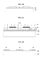
- FIGs. 5A to 5D are cross sectional views illustrating a method for manufacturing an organic light emitting diode display according to the first embodiment of the present disclosure.
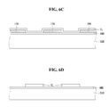
- FIGs. 6A to 6D are cross sectional views illustrating a method for manufacturing an organic light emitting diode display according to the second embodiment of the present disclosure.
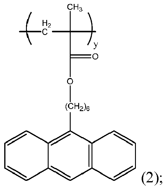
- the highly fluorinated photoresist according to the present disclosure includes a copolymer that is synthesized from two monomers, 3,3,4,4,5,5,6,6,7,7,8,8,9,9,10,10-Heptadecafluorodecyl Methacrylate (FDMA) and 6-(anthracene-9-yl)hexyl methacrylate (AHMA):
- FDMA 3,3,4,4,5,5,6,6,7,7,8,8,9,9,10,10-Heptadecafluorodecyl Methacrylate
- AHMA 6-(anthracene-9-yl)hexyl methacrylate
- x:y is a ratio of monomer FDMA to monomer AHMA used in synthesizing the co-polymer.
- FDMA has a molecular weight of 532.19
- AHMA has a molecular weight of 346.46.
- the resulting photoresist co-polymer formed from FDMA and AHMA is a statistical or random co-polymer and can be represented with the following chemical formula, where r refers to the random nature of the co-polymer:
- FIG. 3 is a schematic view illustrating steps for synthesizing a highly fluorinated photoresist according to the present disclosure.
- Tetrakis(triphenylphosphine)palladium(0) (Pd(PPh3)4) (0.44g, 0.38mmol) was added into the second flask and the bubbling process was performed three times again.
- the mixture of the 5-Hexenyl acetate and the 9-BBN of the first flask was put together with the mixture of the second flask, under N 2 gas condition, to perform a reaction process under a temperature of 85C for 18 hours. After the reaction, the temperature was lowered to room temperature , and the reaction was completed by adding distilled water (22.85ml) and the toluene (57.14ml). After that, using HCl, a neutralization process was performed.
- FDMA (4.00g) and AHMA (0.65g) were put into a tube of 25cm 3 .
- ⁇ , ⁇ , ⁇ -trifluorotoluene(5.00cm 3 ) and purified AIBN (0.048g) were added.
- a N 2 substitution process was performed through three freeze-thaw cycles. After nitrogen substitution, under N 2 gas condition, the solution was stirred for 12 hours under a temperature of 72 degrees C. After that, a precipitation process was performed using Hexane and the solvent was removed in a vacuum oven, there resulting in a white powder synthesized material (3.834g).
- the FDMA-AHMA co-polymer was synthesized using the same fixed mass of FDMA (4.00g) but with different masses of AHMA, such as with AHMA masses of 0.50g, 1.00g, 1.50g and 2.00g.
- Table 1 FDMA mass (g) AHMA mass (g) molecular ratio of FDMA to AHMA 4 g 0.5 g 1:0.19 4 g 0.65 g 1:0.25 4 g 1.0 g 1:0.38 4 g 1.5 g 1:0.58 4 g 2.0 g 1:0.77
- FIG. 4 is a schematic view illustrating the change of the soluability characteristics of the highly fluorinated photoresist by the wavelengths of ultraviolet light according to the present disclosure.
- HFEs hydrofluoroethers
- FIG. 4 just after being synthesized, the novel highly fluorinated photoresist was soluble in hydrofluoroethers (HFEs). However, after being exposed to an ultraviolet light of 365nm wavelength, the structure of the highly fluorinated photoresist was changed so that it became insoluble in hydrofluoroethers (HFEs).
- FIGs. 5A to 5D are cross sectional views illustrating a method for manufacturing an organic light emitting diode display according to the first embodiment of the present disclosure.
- an anode electrode ANO is deposited on a substrate SUB.
- the thin film transistor may first be formed. After that, the anode electrode ANO is formed to connect to the drain electrode of the thin film transistor.
- the present embodiment is related to the method for patterning the organic light emitting material, the explanation for other elements of the display including thin film transistor may not be mentioned in detail.
- an organic light emitting material is deposited to form an organic light emitting layer EL.
- the highly fluorinated photoresist PR is deposited.
- a first ultraviolet light UV1 having a wavelength of 365nm is radiated over the mask MA.
- some portions of the photoresist PR are exposed to the first ultraviolet light UV1 and other portions of the photoresist PR are not affected by the first ultraviolet light UV1.
- the portions of the photoresist PR exposed by the first ultraviolet light UV1 change into an insoluble photoresist IPR.
- the portions not exposed by the first ultraviolet light UV1 are unchanged and remain as the soluble photoresist SPR.
- the soluble photoresist SPR After exposure, by developing the photoresist PR with a fluorinated solvent such as hydrofluoroethers, the soluble photoresist SPR may be removed. However, the insoluble photoresist IPR remains on the organic light emitting layer EL, as shown in FIG. 5B .
- the organic light emitting layer EL is patterned.
- the organic light emitting layer EL can be formed into the same pattern as the insoluble photoresist IPR, as shown in FIG. 5C .
- the insoluble photoresist IPR may be removed, as shown in FIG. 5D .
- the insoluble photoresist IPR is formed on the organic light emitting layer EL by the pattern of the mask MA and the organic light emitting layer EL is patterned according to the shape of the insoluble photoresist IPR.
- FIGs. 6A to 6D are cross sectional views illustrating a method for manufacturing an organic light emitting diode display according to the second embodiment of the present disclosure.
- an anode electrode ANO is deposited on a substrate SUB.
- the thin film transistor may first be formed. After that, the anode electrode ANO is formed to connect to the drain electrode of the thin film transistor.
- the present embodiment is related to the method for patterning the organic light emitting material, the explanation for other elements of the display including thin film transistors may not be mentioned in detail.
- the highly fluorinated photoresist PR As shown in FIG. 6A , on the anode electrode ANO, the highly fluorinated photoresist PR according to the present disclosure is deposited. After positioning a mask MA having a pre-determined mask pattern over the photoresist PR, a first ultraviolet light UV1 having wavelength of 365nm is radiated over the mask MA. Then, according to the pattern of the mask MA, some portions of the photoresist PR are exposed to the first ultraviolet light UV1, and other portions of the photoresist PR are not influenced by the first ultraviolet light UV1. Due to the characteristics of the photoresist PR according to the present disclosure, the portions exposed by the first ultraviolet light UV1 may be changed into the insoluble photoresist IPR. On the contrary, the portions not exposed by the first ultraviolet light UV1 are not changed and remain as the soluble photoresist SPR.
- the soluble photoresist SPR After exposure, by developing the photoresist PR with a fluorinated solvent such as hydrofluoroethers, the soluble photoresist SPR may be removed. However, the insoluble photoresist IPR remains on the organic light emitting layer EL, as shown in FIG. 6B .
- an organic light emitting layer EL By depositing an organic light emitting material over whole surface of the substrate SUB and the insoluble photoresist IPR, an organic light emitting layer EL can be formed, as shown in FIG. 6C . Even though it is not shown in the figures, the insoluble photoresist IPR may have the reversed tapered shape at its edges.
- the insoluble photoresit IPR is stripped out.
- portions of the organic light emitting layer EL deposited on the soluble photoresist IPR are also removed.
- the portions of the organic light emitting layer EL contacting the anode electrode ANO remain so that the pattern is completed, as shown in FIG. 6D .
- a highly fluorinated solvent such as hydrofluoroethers can be used when developing the photoresist.
- the exposed portions of the photoresist IPR exposed by the mask MA remain, and the organic light emitting layer EL is formed into a pattern that is the reverse of the insoluble photoresist IPR.
- the organic light emitting material may include materials emitting red, green or blue color light or include material emitting white color light.
- a color filter is deposited on the organic light emitting material layer, and the color filter may be patterned using the highly fluorinated photoresist according to the present disclosure.
- the manufacturing method according to the present disclosure prevents the organic light emitting material from being damaged during the patterning process by patterning the photoresist without using a photo acid generator (PAG). Additionally, the photoresist according to the present disclosure can be used not only for patterning the organic light emitting material but also for patterning the other layers.
- PAG photo acid generator
Landscapes
- Physics & Mathematics (AREA)
- General Physics & Mathematics (AREA)
- Chemical & Material Sciences (AREA)
- Spectroscopy & Molecular Physics (AREA)
- Health & Medical Sciences (AREA)
- Chemical Kinetics & Catalysis (AREA)
- Medicinal Chemistry (AREA)
- Polymers & Plastics (AREA)
- Organic Chemistry (AREA)
- Engineering & Computer Science (AREA)
- Manufacturing & Machinery (AREA)
- Electroluminescent Light Sources (AREA)
Abstract
Description
- This application claims the benefit of Korea Patent Application No.
10-2012-0138223 filed on November 30, 2012 - The present disclosure relates to a highly fluorinated photoresist employing a photodimerization chemistry and a method for manufacturing an organic light emitting diode display using the same.
- Nowadays, various flat panel display devices are developed for overcoming many drawbacks of the cathode ray tube such as heavy weight and bulk volume. The flat panel display devices include the liquid crystal display device (or LCD), the field emission display (or FED), the plasma display panel (or PDP) and the electroluminescence device (or EL).
-
FIG. 1 is a plane view illustrating the structure of the organic light emitting diode display (or 'OLED') having active switching elements such as thin film transistors according to the related art.FIG.2 is a cross sectional view illustrating the structure of the OLED along to the cutting line of I-I" inFIG. 1 according to the related art. - Referring to
FIGs. 1 and2 , the OLED display comprises a thin film transistor (or 'TFT') substrate having the thin film transistors ST and DT and an organic light emitting diode OLED connected to and driven by the thin film transistors ST and DT, and a cap ENC joining the TFT substrate with an organic adhesive POLY (not shown) therebetween. The TFT substrate includes a switching thin film transistor ST, a driving thin film transistor DT connected to the switching thin film transistor ST, and an organic light emitting diode OLED connected to the driving thin film transistor DT. - On a transparent substrate SUB, the switching thin film transistor ST is formed where a gate line GL and a data line DL cross each other. The switching thin film transistor ST selects the pixel which is connected to the switching thin film transistor ST. The switching thin film transistor ST includes a gate electrode SG branching from the gate line GL, a semiconductor channel layer SA overlapping with the gate electrode SG, a source electrode SS and a drain electrode SD. The driving thin film transistor DT drives an anode electrode ANO of the organic light emitting diode OD disposed at the pixel selected by the switching thin film transistor ST. The driving thin film transistor DT includes a gate electrode DG connected to the drain electrode SD of the switching thin film transistor ST, a semiconductor channel layer DA, a source electrode DS connected to the driving current line VDD, and a drain electrode DD. The drain electrode DD of the driving thin film transistor DT is connected to the anode electrode ANO of the organic light emitting diode OD.
- As one example,
FIG. 2 shows the thin film transistor of top gate structure. In this case, the semiconductor channel layers SA and DA of the switching thin film transistor ST and the driving thin film transistor DT are firstly formed on the substrate SUB and the gate insulating layer GI covering them and then the gate electrodes SG and DG are formed thereon by overlapping with the center portion of the semiconductor channel layers SA and DA. After that, at both sides of the semiconductor channel layers SA and DA, the source electrodes SS and DS and the drain electrodes SD and DD are connected thereto through contact holes penetrating an insulating layer IN. The source electrodes SS and DS and the drain electrodes SD and DD are formed on the insulating layer IN. - In addition, at the outer area surrounding the display area where the pixel area is disposed, a gate pad GP formed at one end of the gate line GL, a data pad DP formed at one end of the data line DL, and a driving current pad VDP formed at one end of the driving current line VDD are arrayed. A passivation layer PAS is disposed to cover the upper whole surface of the substrate SUB having the switching and the driving thin film transistors ST and DT. After that, the contact holes are formed to expose the gate pad GP, the data pad DP, the driving current pad VDP and the drain electrode DD of the driving thin film transistor DD. Over the display area within the substrate SUB, a planar layer PL is coated. The planar layer PL makes the roughness of the upper surface of the substrate SUB in much smoother condition, for coating the organic materials composing the organic light emitting diode on the smooth and planar surface condition of the substrate SUB.
- On the planar layer PL, the anode electrode ANO is formed to connect the drain electrode DD of the driving thin film transistor DT through one of the contact holes. On the other hand, at the outer area of the display area not having the planar layer PL, formed are a gate pad electrode GPT, a data pad electrode DPT and a driving current electrode VDPT connected to the gate pad GP, the data pad DP and the driving current pad VDP, respectively, exposed through the contact holes. On the substrate SUB, a bank BA is formed covering the display area, excepting the pixel area. Finally, a spacer SP may be formed over some portion of the bank BA.
- A cap ENC is joined to the TFT substrate. In that case, it is preferable that the TFT substrate and the cap ENC are completely sealed by having an organic adhesive between them. The gate pad electrode GPT and the data pad electrode DPT are exposed and may be connected to external devices via the various connecting means.
- As the needs for the organic light emitting diode display increase, and more advanced manufacturing technologies are developing, the technologies for the high resolution and large area organic light emitting diode displays has become underdeveloped. Until now, there are some methods for forming organic light emitting diodes on a large glass substrate, i.e., the fine metal mask (or 'FMM') patterning technology, the ink-jet printing technology, and the laser patterning technology. As an alternative method for manufacturing a large area organic light emitting diode display, a method for depositing one large white organic light emitting diode layer with a patterned color filter layer can also be used.
- Using these patterning technologies or methods, it is possible to manufacture an organic light emitting diode display having large area and high resolution. However, the production yields and/or costs are not acceptable for mass production. In order to manufacture the pixel area of high resolution on a large area substrate, the most reasonable method is the photolithography method. There is still a critical problem for using the photolithography technology when patterning the organic light emitting materials. For example, the organic light emitting material can be easily damaged by the photoresist itself and the solvent used for developing and/or removing the photoresist.
- In order to overcome the above mentioned drawbacks, the purpose of the present disclosure is to suggest a highly fluorinated photoresist which is less interactive with organic light emitting materials, and a method for manufacturing an organic light emitting diode display using the same photoresist. Another purpose of the present disclosure is to suggest a highly fluorinated photoresist which is changing the solubility by the photodimerization reaction of anthracene to minimize the damage of the organic light emitting diode material, and a method for manufacturing an organic light emitting diode display using the same photoresist.
- In one embodiment, a copolymer for a photoresist is disclosed. The copolymer is formed by a process that includes providing a first monomer represented by formula (1) and a second monomer represented by formula (2)
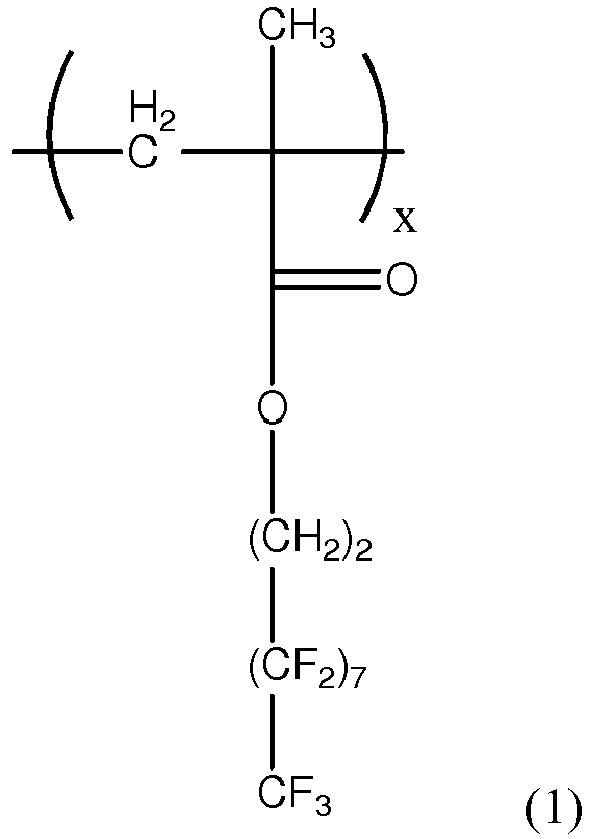

- In one embodiment, x:y is selected from the range of x:y = 1:0.19 to x:y = 1:0.77. In some embodiments, x:y can be 1:0.19, x:y can be 1:0.25, x:y can be 1:0.38, x:y can be 1:0.58, or x:y can be 1:0.77.
- In one embodiment, the present disclosure includes a method for manufacturing an organic light emitting diode display comprising: forming an electrode on a substrate; depositing an organic light emitting layer on the electrode; depositing a photoresist on the organic light emitting layer, the photoresist including the above mentioned copolymer; patterning the photoresist into a patterned photoresist by exposing the photoresist to an ultraviolet light through a mask; patterning the organic light emitting layer into a patterned organic light emitting layer using the patterned photoresist; and stripping the patterned photoresist.
- In one embodiment, the present disclosure includes a method for manufacturing an organic light emitting diode display comprising: forming an electrode on a substrate; depositing a photoresist on the electrode, the photoresist including the above mentioned copolymer; patterning the photoresist into a patterned photoresist by exposing the photoresist to an ultraviolet light through a mask; depositing an organic light emitting layer on the patterned photoresist and the electrode; and removing the patterned photoresist and portions of the organic light emitting layer on the patterned photoresist.
- In one embodiment, the ultraviolet light has a wavelength of 365nm. In one embodiment, the photoresist is patterned with a fluorinated solvent.
- The highly fluorinated photoresist according to the present disclosure has the characteristics in which its solubility is changed by the photodimerization reaction of anthracene and less interaction with organic light emitting materials. As it has no anthracence, any strong acid material is not be formed when developing the photoresist. As a result, by using the highly fluorinated photoresist less interaction with the organic light emitting materials, it is possible to manufacture the organic light emitting diode display having the high resolution on the large area substrate. Furthermore, in the method for manufacturing the organic light emitting diode display according to the present disclosure, as it is possible to use the same material when developing the photoresist and removing the photoresist, the manufacturing process can be simple, the cost may be reduced, and the production yield may be high.
- The accompanying drawings, which are included to provide a further understanding of the invention and are incorporated in and constitute a part of this specification, illustrate embodiments of the invention and together with the description serve to explain the principles of the invention.
- In the drawings:
-
FIG. 1 is the plane view illustrating the organic light emitting diode display using the thin film transistor according to the related art. -
FIG. 2 is the cross sectional view illustrating the structure of the organic light emitting diode display cutting along the line I-I' inFIG. 1 , according to the related art a back light unit generating the collimated light beam using a collimation lens. -
FIG. 3 is a schematic view illustrating steps for synthesizing a highly fluorinated photoresist according to the present disclosure. -
FIG. 4 is a schematic view illustrating the change of the soluability characteristics of the highly fluorinated photoresist by the wavelengths of the ultralight according to the present disclosure. -
FIGs. 5A to 5D are cross sectional views illustrating a method for manufacturing an organic light emitting diode display according to the first embodiment of the present disclosure. -
FIGs. 6A to 6D are cross sectional views illustrating a method for manufacturing an organic light emitting diode display according to the second embodiment of the present disclosure. - Embodiments of the present disclosure are explained herein by references to the figures. Like reference numerals designate like elements throughout the detailed description. However, the present disclosure is not restricted by these embodiments but can be applied to various changes or modifications without changing the technical spirit. In the following embodiments, the names of the elements are selected by considering the easiness for explanation so that they may be different from actual names.
- At first, a novel highly fluorinated photoresist will be explained. The highly fluorinated photoresist according to the present disclosure includes a copolymer that is synthesized from two monomers, 3,3,4,4,5,5,6,6,7,7,8,8,9,9,10,10-Heptadecafluorodecyl Methacrylate (FDMA) and 6-(anthracene-9-yl)hexyl methacrylate (AHMA):


- where x:y is a ratio of monomer FDMA to monomer AHMA used in synthesizing the co-polymer. In one embodiment, x:y is selected from the range of x:y = 1:0.1 to x:y = 1:1, as explained below. In one embodiment, FDMA has a molecular weight of 532.19, and AHMA has a molecular weight of 346.46.
- In one embodiment the resulting photoresist co-polymer formed from FDMA and AHMA is a statistical or random co-polymer and can be represented with the following chemical formula, where r refers to the random nature of the co-polymer:

- Hereinafter, referring to
FIG. 3 , we will explain an example for synthesizing the highly fluorinated photoreist copolymer according to the present disclosure. The following description is just one example of synthesizing a copolymer so that the present disclosure is not limited by this example.FIG. 3 is a schematic view illustrating steps for synthesizing a highly fluorinated photoresist according to the present disclosure. - 1) The synthesizing of 6-(anthracen-9-yl)hexan-1-ol (AHOH).
- 5-Hexenyl acetate (2.00g, 14.06mmol) and 9-Borabicyclo[3.3.1]nonane (0.5M solution in THF) (9-BBN) (25.21g, 14.06mmol) were put into a first flask of 250ml. A stirring process was then performed for 3 hours at room temperature under N2 gas condition. After putting 3M NaOH solution (9.14ml), 9-Bromoanthracene (3.30g, 12.80mmol), and THF anhydrous (25cm3) into a second flask of 100ml, a bubbling process was performed three times. After that, Tetrakis(triphenylphosphine)palladium(0) (Pd(PPh3)4) (0.44g, 0.38mmol) was added into the second flask and the bubbling process was performed three times again. The mixture of the 5-Hexenyl acetate and the 9-BBN of the first flask was put together with the mixture of the second flask, under N2 gas condition, to perform a reaction process under a temperature of 85C for 18 hours. After the reaction, the temperature was lowered to room temperature , and the reaction was completed by adding distilled water (22.85ml) and the toluene (57.14ml). After that, using HCl, a neutralization process was performed. With EA and brine, the work-up process was performed to the neutralized product. Using MgSO4, moisture was removed. After purifying this compositing material, using Hexane (30cm3) and toluene (10cm3), a recrystalization process was performed. After filtering and drying the material in the vacuum oven, a yellow powder synthesized (or 'composition') material (2.78g, 71%) was acquired.
- 2) The synthesizing of AHMA.
- The synthesized 6-(anthracen-9-yl)hexan-1-ol (AHOH) (2.78g, 10.00mmol), 4-Dimethylaminopyridine (DMAP) (1.830g, 14.98mmol), 2,6-Di-Tert-butyl-4-methylphenol (BHT) (polymerization inhibitor, 0.01g), Methacrylic anhydride (3.079g, 1997mmol), and DCM anhydrous (30cm3) were put into a flask of 250ml. A stirring process was then performed for 4 hours under room temperature. After that, MeOH (1cm3) was added, and a stirring process was performed again for 1 hour. After purifying the composition material, an oil type synthesized material (1.94g, 56%) having a light yellow color was acquired.
- 3) The synthesizing of the FDMA-AHMA co-polymer.
- FDMA (4.00g) and AHMA (0.65g) were put into a tube of 25cm3. α,α,α-trifluorotoluene(5.00cm3) and purified AIBN (0.048g) were added. After sealing the tube, using a vacuum pump and N2 gas, a N2 substitution process was performed through three freeze-thaw cycles. After nitrogen substitution, under N2 gas condition, the solution was stirred for 12 hours under a temperature of 72 degrees C. After that, a precipitation process was performed using Hexane and the solvent was removed in a vacuum oven, there resulting in a white powder synthesized material (3.834g).
- In other embodiments, the FDMA-AHMA co-polymer was synthesized using the same fixed mass of FDMA (4.00g) but with different masses of AHMA, such as with AHMA masses of 0.50g, 1.00g, 1.50g and 2.00g. The following table illustrates different combinations of FDMA and AHMA used in synthesizing the FDMA-AHMA co-polymer:
Table 1 FDMA mass (g) AHMA mass (g) molecular ratio of FDMA to AHMA 4 g 0.5 g 1:0.19 4 g 0.65 g 1:0.25 4 g 1.0 g 1:0.38 4 g 1.5 g 1:0.58 4 g 2.0 g 1:0.77 - Each of the FDMA-AHMA copolymers from Table 1 was tested and found to have the same photo characteristics. Specifically, the photo characteristics of the co-polymer used as the novel synthesized highly fluorinated photoresist is shown in
FIG. 4. FIG. 4 is a schematic view illustrating the change of the soluability characteristics of the highly fluorinated photoresist by the wavelengths of ultraviolet light according to the present disclosure. Referring toFIG. 4 , just after being synthesized, the novel highly fluorinated photoresist was soluble in hydrofluoroethers (HFEs). However, after being exposed to an ultraviolet light of 365nm wavelength, the structure of the highly fluorinated photoresist was changed so that it became insoluble in hydrofluoroethers (HFEs). - Hereinafter, referring to
FIGs. 5A to 5D , a method for manufacturing an organic light emitting diode display according to the first embodiment of the present disclosure is now explained.FIGs. 5A to 5D are cross sectional views illustrating a method for manufacturing an organic light emitting diode display according to the first embodiment of the present disclosure. - On a substrate SUB, an anode electrode ANO is deposited. For the case of the active type organic light emitting diode display, as shown in
FIGs. 1 and2 , the thin film transistor may first be formed. After that, the anode electrode ANO is formed to connect to the drain electrode of the thin film transistor. As the present embodiment is related to the method for patterning the organic light emitting material, the explanation for other elements of the display including thin film transistor may not be mentioned in detail. - As shown in
FIG. 5A , on the anode electrode ANO, an organic light emitting material is deposited to form an organic light emitting layer EL. On the organic light emitting layer EL, the highly fluorinated photoresist PR is deposited. After positioning a mask MA having a pre-determined mask pattern over the photoresist PR, a first ultraviolet light UV1 having a wavelength of 365nm is radiated over the mask MA. Then, according to the pattern of the mask MA, some portions of the photoresist PR are exposed to the first ultraviolet light UV1 and other portions of the photoresist PR are not affected by the first ultraviolet light UV1. Due to the characteristics of the highly fluorinated photoresist PR, the portions of the photoresist PR exposed by the first ultraviolet light UV1 change into an insoluble photoresist IPR. On the contrary, the portions not exposed by the first ultraviolet light UV1 are unchanged and remain as the soluble photoresist SPR. - After exposure, by developing the photoresist PR with a fluorinated solvent such as hydrofluoroethers, the soluble photoresist SPR may be removed. However, the insoluble photoresist IPR remains on the organic light emitting layer EL, as shown in
FIG. 5B . - Using the insoluble photoresist IPR as a mask, the organic light emitting layer EL is patterned. Thus, the organic light emitting layer EL can be formed into the same pattern as the insoluble photoresist IPR, as shown in
FIG. 5C . - After that, using a chemical stripper, the insoluble photoresist IPR may be removed, as shown in
FIG. 5D . In the photolithography process according to the first embodiment of the present disclosure, the insoluble photoresist IPR is formed on the organic light emitting layer EL by the pattern of the mask MA and the organic light emitting layer EL is patterned according to the shape of the insoluble photoresist IPR. - Hereinafter, referring to
FIGs. 6A to 6D , we will explain a method for manufacturing an organic light emitting diode display according to the second embodiment of the present disclosure.FIGs. 6A to 6D are cross sectional views illustrating a method for manufacturing an organic light emitting diode display according to the second embodiment of the present disclosure. - On a substrate SUB, an anode electrode ANO is deposited. For the case of the active type organic light emitting diode display, as shown in
FIGs. 1 and2 , the thin film transistor may first be formed. After that, the anode electrode ANO is formed to connect to the drain electrode of the thin film transistor. As the present embodiment is related to the method for patterning the organic light emitting material, the explanation for other elements of the display including thin film transistors may not be mentioned in detail. - As shown in
FIG. 6A , on the anode electrode ANO, the highly fluorinated photoresist PR according to the present disclosure is deposited. After positioning a mask MA having a pre-determined mask pattern over the photoresist PR, a first ultraviolet light UV1 having wavelength of 365nm is radiated over the mask MA. Then, according to the pattern of the mask MA, some portions of the photoresist PR are exposed to the first ultraviolet light UV1, and other portions of the photoresist PR are not influenced by the first ultraviolet light UV1. Due to the characteristics of the photoresist PR according to the present disclosure, the portions exposed by the first ultraviolet light UV1 may be changed into the insoluble photoresist IPR. On the contrary, the portions not exposed by the first ultraviolet light UV1 are not changed and remain as the soluble photoresist SPR. - After exposure, by developing the photoresist PR with a fluorinated solvent such as hydrofluoroethers, the soluble photoresist SPR may be removed. However, the insoluble photoresist IPR remains on the organic light emitting layer EL, as shown in
FIG. 6B . - By depositing an organic light emitting material over whole surface of the substrate SUB and the insoluble photoresist IPR, an organic light emitting layer EL can be formed, as shown in
FIG. 6C . Even though it is not shown in the figures, the insoluble photoresist IPR may have the reversed tapered shape at its edges. - After depositing the organic light emitting layer EL, the insoluble photoresit IPR is stripped out. At the same time, portions of the organic light emitting layer EL deposited on the soluble photoresist IPR are also removed. As a result, the portions of the organic light emitting layer EL contacting the anode electrode ANO remain so that the pattern is completed, as shown in
FIG. 6D . In the second embodiment of the present disclosure, a highly fluorinated solvent such as hydrofluoroethers can be used when developing the photoresist. Furthermore, in the photolithography process according to the second embodiment of the present disclosure, the exposed portions of the photoresist IPR exposed by the mask MA remain, and the organic light emitting layer EL is formed into a pattern that is the reverse of the insoluble photoresist IPR. - In the first and second embodiments of the present disclosure, by patterning the organic light emitting layer using the highly fluorinated photoresist, the method for manufacturing the organic light emitting diode display is explained. The organic light emitting material may include materials emitting red, green or blue color light or include material emitting white color light. For example, for the case of the white color light, a color filter is deposited on the organic light emitting material layer, and the color filter may be patterned using the highly fluorinated photoresist according to the present disclosure.
- The manufacturing method according to the present disclosure prevents the organic light emitting material from being damaged during the patterning process by patterning the photoresist without using a photo acid generator (PAG). Additionally, the photoresist according to the present disclosure can be used not only for patterning the organic light emitting material but also for patterning the other layers.
- While the embodiment of the present invention has been described in detail with reference to the drawings, it will be understood by those skilled in the art that the invention can be implemented in other specific forms without changing the technical spirit or essential features of the invention. Therefore, it should be noted that the forgoing embodiments are merely illustrative in all aspects and are not to be construed as limiting the invention. The scope of the invention is defined by the appended claims rather than the detailed description of the invention. All changes or modifications or their equivalents made within the meanings and scope of the claims should be construed as falling within the scope of the invention.
Claims (15)
- A copolymer of a photoresist formed by the process comprising:providing a first monomer represented by formula (1) and a second monomer represented by formula (2)

 forming the copolymer from the first monomer and the second monomer, where x:y is
a ratio of the first monomer to the second monomer and x:y is selected from the range of x:y = 1:0.1 to x:y = 1:1. - The copolymer according to claim 1 wherein x:y is selected from the range of x:y = 1:0.19 to x:y = 1:0.77.
- The copolymer according to claim 1 and/or claim 2 wherein x:y is 1:0.19.
- The copolymer according to claim 1 and/or claim 2 wherein x:y is 1:0.25.
- The copolymer according to claim 1 and/or claim 2 wherein x:y is 1:0.38.
- The copolymer according to claim 1 and/or claim 2 wherein x:y is 1:0.58.
- The copolymer according to claim 1 and/or claim 2 wherein x:y is 1:0.77.
- A method for manufacturing an organic light emitting diode display comprising:forming an electrode on a substrate;depositing an organic light emitting layer on the electrode;depositing a photoresist on the organic light emitting layer, the photoresist including a copolymer formed by the process comprising:providing a first monomer represented by formula (1) and a second monomer represented by formula (2)

 forming the copolymer from the first monomer and the second monomer, where x:y is a ratio of the first monomer to the second monomer and x:y is selected from the range of x:y = 1:0.1 to x:y = 1:1;patterning the photoresist into a patterned photoresist by exposing the photoresist to ultraviolet light using a mask;patterning the organic light emitting layer into a patterned organic light emitting layer using the patterned photoresist; andstripping the patterned photoresist.
 - The method according to claim 8, wherein the ultraviolet light has a wavelength of 365nm.
- The method according to claim 8 and/or claim 9, wherein the photoresist is patterned using a fluorinated solvent.
- The method according to any one of claims 8 to 10, wherein x:y is selected from the range of x:y = 1:0.19 to x:y = 1:0.77.
- A method for manufacturing an organic light emitting diode display comprising:forming an electrode on a substrate;depositing a photoresist on the electrode, the photoresist including a copolymer formed by the process comprising:providing a first monomer represented by formula (1) and a second monomer represented by formula (2)

 forming the copolymer from the first monomer and the second monomer, where x:y is a ratio of the first monomer to the second monomer and x:y is selected from the range of x:y = 1:0.1 to x:y = 1:1;patterning the photoresist into a patterned photoresist by exposing the photoresist to ultraviolet light using a mask;depositing an organic light emitting layer on the patterned photoresist and the electrode; andremoving the patterned photoresist and portions of the organic light emitting layer on the patterned photoresist.
 - The method according to claim 12, wherein the ultraviolet light has a wavelength of 365nm.
- The method according to claim 12 and/or claim 13, wherein the photoresist is patterned using a fluorinated solvent.
- The method according to any one of claims 12 to 14, wherein x:y is selected from the range of x:y = 1:0.19 to x:y = 1:0.77.
Applications Claiming Priority (1)
| Application Number | Priority Date | Filing Date | Title |
|---|---|---|---|
| KR1020120138223A KR101420527B1 (en) | 2012-11-30 | 2012-11-30 | Photoresist Employing Photodimerization Chemistry and Method For Manufacturing Organic Light Emitting Diode Display Using The Same |
Publications (2)
| Publication Number | Publication Date |
|---|---|
| EP2738604A1 true EP2738604A1 (en) | 2014-06-04 |
| EP2738604B1 EP2738604B1 (en) | 2014-12-31 |
Family
ID=48670382
Family Applications (1)
| Application Number | Title | Priority Date | Filing Date |
|---|---|---|---|
| EP13171836.3A Active EP2738604B1 (en) | 2012-11-30 | 2013-06-13 | Photoresist employing photodimerization chemistry and method for manufacturing organic light emitting diode display using the same |
Country Status (5)
| Country | Link |
|---|---|
| US (2) | US9147842B2 (en) |
| EP (1) | EP2738604B1 (en) |
| KR (1) | KR101420527B1 (en) |
| CN (1) | CN103852974B (en) |
| TW (1) | TWI480693B (en) |
Cited By (1)
| Publication number | Priority date | Publication date | Assignee | Title |
|---|---|---|---|---|
| EP2918616A1 (en) * | 2014-03-14 | 2015-09-16 | Solvay SA | Photosensitive polymer resin, photosensitive resin composition comprising the same, and layer made therefrom |
Families Citing this family (9)
| Publication number | Priority date | Publication date | Assignee | Title |
|---|---|---|---|---|
| US10503065B2 (en) | 2014-08-01 | 2019-12-10 | Orthogonal, Inc. | Photolithographic patterning of devices |
| JP6653315B2 (en) | 2014-08-01 | 2020-02-26 | オーソゴナル,インコーポレイテッド | Photolithographic patterning of organic electronic devices |
| JP2017526177A (en) | 2014-08-01 | 2017-09-07 | オーソゴナル,インコーポレイテッド | Method for photolithographic patterning of devices |
| WO2016019277A1 (en) | 2014-08-01 | 2016-02-04 | Orthogonal, Inc. | Photolithographic patterning of organic electronic devices |
| KR101784104B1 (en) * | 2016-04-28 | 2017-10-10 | 인하대학교 산학협력단 | Preparing method of organic light emitting diode device using perfluorinated photoresist polymers with narrow molecular weight distribution |
| KR102079016B1 (en) * | 2018-02-08 | 2020-02-19 | 인하대학교 산학협력단 | Fluorous Developer Solutions with Additives for Highly Fluorinated Photoresists and Processing Method for Organic Light-Emitting Diodes display |
| KR102114117B1 (en) * | 2018-11-27 | 2020-05-22 | 인하대학교 산학협력단 | Manufacture of positive-tone photoresist materials using highly fluorinated monomolecular photoresist and highly fluorinated amine derivatives having solubility in high fluorine solvent |
| KR102682395B1 (en) | 2018-12-26 | 2024-07-09 | 삼성디스플레이 주식회사 | Organic light emitting display apparatus and method of manufacturing the same |
| CN118235092A (en) * | 2021-11-15 | 2024-06-21 | 日产化学株式会社 | Polycyclic aromatic hydrocarbon-based photocurable resin composition |
Citations (3)
| Publication number | Priority date | Publication date | Assignee | Title |
|---|---|---|---|---|
| EP0040841A1 (en) * | 1980-05-27 | 1981-12-02 | Daikin Kogyo Co., Ltd. | Photosensitive material |
| US20100222526A1 (en) * | 2009-02-27 | 2010-09-02 | Maruzen Petrochemical Co., Ltd. | Method for producing a copolymer for photoresist |
| WO2012074076A1 (en) * | 2010-12-01 | 2012-06-07 | 日産化学工業株式会社 | Fluorine-containing hyperbranched polymer, and photo-sensitive composition containing same |
Family Cites Families (3)
| Publication number | Priority date | Publication date | Assignee | Title |
|---|---|---|---|---|
| JP3748596B2 (en) * | 1995-08-02 | 2006-02-22 | 富士通株式会社 | Resist material and resist pattern forming method |
| ATE541242T1 (en) * | 2007-01-22 | 2012-01-15 | Nissan Chemical Ind Ltd | POSITIVE LIGHT SENSITIVE RESIN COMPOSITION |
| KR101507166B1 (en) * | 2008-12-08 | 2015-04-30 | 엘지디스플레이 주식회사 | Blue light emitting compounds and organic electroluminescent devices containing them |
-
2012
- 2012-11-30 KR KR1020120138223A patent/KR101420527B1/en active Active
-
2013
- 2013-05-28 US US13/903,657 patent/US9147842B2/en active Active
- 2013-06-13 EP EP13171836.3A patent/EP2738604B1/en active Active
- 2013-07-01 TW TW102123537A patent/TWI480693B/en active
- 2013-07-12 CN CN201310292187.2A patent/CN103852974B/en active Active
-
2015
- 2015-08-19 US US14/830,034 patent/US9666802B2/en active Active
Patent Citations (3)
| Publication number | Priority date | Publication date | Assignee | Title |
|---|---|---|---|---|
| EP0040841A1 (en) * | 1980-05-27 | 1981-12-02 | Daikin Kogyo Co., Ltd. | Photosensitive material |
| US20100222526A1 (en) * | 2009-02-27 | 2010-09-02 | Maruzen Petrochemical Co., Ltd. | Method for producing a copolymer for photoresist |
| WO2012074076A1 (en) * | 2010-12-01 | 2012-06-07 | 日産化学工業株式会社 | Fluorine-containing hyperbranched polymer, and photo-sensitive composition containing same |
Non-Patent Citations (3)
| Title |
|---|
| BRATSCHKOV C ET AL: "SYNTHESIS AND PHOTOCHEMICAL TRANSFORMATIONS OF AN ANTHRACENE CONTAINING METHACRYLIC COPOLYMER", POLYMER BULLETIN, SPRINGER, HEIDELBERG, DE, vol. 46, no. 5, 1 June 2001 (2001-06-01), pages 345 - 349, XP001068048, ISSN: 0170-0839, DOI: 10.1007/S002890170041 * |
| HENRI BOUAS-LAURENT ET AL: "Photodimerization of anthracenes in fluid solution: structural aspects", CHEMICAL SOCIETY REVIEWS, vol. 29, no. 1, 1 January 2000 (2000-01-01), pages 43 - 55, XP055102953, ISSN: 0306-0012, DOI: 10.1039/a801821i * |
| JEFERSON FERREIRA DE DEUS ET AL: "Photo and electroluminescence studies of poly(methyl methacrylate-co-9-anthryl methyl methacrylate)", CHEMICAL PHYSICS, vol. 297, no. 1-3, 1 February 2004 (2004-02-01), pages 177 - 186, XP055102959, ISSN: 0301-0104, DOI: 10.1016/j.chemphys.2003.10.023 * |
Cited By (1)
| Publication number | Priority date | Publication date | Assignee | Title |
|---|---|---|---|---|
| EP2918616A1 (en) * | 2014-03-14 | 2015-09-16 | Solvay SA | Photosensitive polymer resin, photosensitive resin composition comprising the same, and layer made therefrom |
Also Published As
| Publication number | Publication date |
|---|---|
| TWI480693B (en) | 2015-04-11 |
| US20140154827A1 (en) | 2014-06-05 |
| KR101420527B1 (en) | 2014-07-17 |
| KR20140072326A (en) | 2014-06-13 |
| EP2738604B1 (en) | 2014-12-31 |
| CN103852974A (en) | 2014-06-11 |
| US9666802B2 (en) | 2017-05-30 |
| TW201421151A (en) | 2014-06-01 |
| CN103852974B (en) | 2016-12-28 |
| US20150357571A1 (en) | 2015-12-10 |
| US9147842B2 (en) | 2015-09-29 |
Similar Documents
| Publication | Publication Date | Title |
|---|---|---|
| EP2738604B1 (en) | Photoresist employing photodimerization chemistry and method for manufacturing organic light emitting diode display using the same | |
| TWI588212B (en) | Triarylmethane compound, colored resin composition, color filter, liquid crystal display and organic el display | |
| KR101703718B1 (en) | Photosensitive resin composition, method for producing cured film, cured film, organic el display device and liquid crystal display device | |
| TWI486404B (en) | Colored resin composition, color filter, liquid crystal display and organic el display | |
| TWI810608B (en) | Coloring composition and compound | |
| EP2613198B1 (en) | Photosensitive resin composition, oxime sulfonate compound, method for forming cured film, cured film, organic el display device, and liquid crystal display device | |
| KR101882722B1 (en) | Positive working photosensitive resin composition | |
| KR101806822B1 (en) | Positive type photosensitive resin composition, method for formation of cured film, cured film, organic el display device, and liquid crystal display device | |
| WO2009107734A1 (en) | Coloring resin composition for color filter, color filter, organic el display and liquid crystal display | |
| KR20150103210A (en) | Photosensitive resin composition, production method for cured film using same, cured film, liquid crystal display device, and organic el display device | |
| CN105301898A (en) | Sensitivity radioactive ray resin composite, hard coating film, formation method thereof, and display element | |
| TWI578107B (en) | Photosensitive resin composition, method for forming cured film, cured film, organic EL display device, and liquid crystal display device | |
| TWI598686B (en) | Photosensitive resin composition, method for producing interlayer insulating film, interlayer insulating film, liquid crystal display device, and organic EL display device | |
| JP2022140456A (en) | photosensitive composition | |
| TW202045627A (en) | Colored resin composition, color filter, and image display device | |
| KR20160022766A (en) | Photo-sensitive resin composition, method of producing cured film, cured film, liquid crystal display device, organic electroluminescence display device and touch panel | |
| JP2011215590A (en) | Method of producing cured film, photosensitive resin composition, cured film, organic el display device, and liquid crystal display device | |
| KR20250039415A (en) | Photosensitive surface treatment agent, laminate, substrate for pattern formation, transistor, pattern formation method and method for manufacturing transistor | |
| JP6763915B2 (en) | Acrylate compounds, photocurable compositions containing them, photocurable cured films and image display devices | |
| JP5885802B2 (en) | Photosensitive resin composition, oxime sulfonate compound, method for forming cured film, cured film, organic EL display device, and liquid crystal display device | |
| KR20150072663A (en) | Random copolymers, methods of forming fine patterns and methods of manufacturing display devices | |
| TW201523132A (en) | Photosensitive resin composition, method for producing cured film, cured film, liquid crystal display device, and organic EL display device | |
| KR101964685B1 (en) | Positive-type photosensitive resin composition, method for forming cured film, cured film, organic el display device, and, liquid crystal display device | |
| JP5335045B2 (en) | Photosensitive resin composition, oxime sulfonate compound, method for forming cured film, cured film, organic EL display device, and liquid crystal display device | |
| CN117813550A (en) | Photosensitive surface treatment agent, laminated body, transistor, pattern forming method, and manufacturing method of transistor |
Legal Events
| Date | Code | Title | Description |
|---|---|---|---|
| PUAI | Public reference made under article 153(3) epc to a published international application that has entered the european phase |
Free format text: ORIGINAL CODE: 0009012 |
|
| 17P | Request for examination filed |
Effective date: 20140327 |
|
| AK | Designated contracting states |
Kind code of ref document: A1 Designated state(s): AL AT BE BG CH CY CZ DE DK EE ES FI FR GB GR HR HU IE IS IT LI LT LU LV MC MK MT NL NO PL PT RO RS SE SI SK SM TR |
|
| AX | Request for extension of the european patent |
Extension state: BA ME |
|
| RIC1 | Information provided on ipc code assigned before grant |
Ipc: G03F 7/038 20060101AFI20140623BHEP Ipc: H01L 51/00 20060101ALN20140623BHEP Ipc: G03F 7/004 20060101ALI20140623BHEP Ipc: C08F 220/24 20060101ALI20140623BHEP |
|
| GRAP | Despatch of communication of intention to grant a patent |
Free format text: ORIGINAL CODE: EPIDOSNIGR1 |
|
| INTG | Intention to grant announced |
Effective date: 20140806 |
|
| RIC1 | Information provided on ipc code assigned before grant |
Ipc: G03F 7/038 20060101AFI20140725BHEP Ipc: C08F 220/24 20060101ALI20140725BHEP Ipc: G03F 7/004 20060101ALI20140725BHEP Ipc: H01L 51/00 20060101ALN20140725BHEP |
|
| GRAS | Grant fee paid |
Free format text: ORIGINAL CODE: EPIDOSNIGR3 |
|
| GRAA | (expected) grant |
Free format text: ORIGINAL CODE: 0009210 |
|
| AK | Designated contracting states |
Kind code of ref document: B1 Designated state(s): AL AT BE BG CH CY CZ DE DK EE ES FI FR GB GR HR HU IE IS IT LI LT LU LV MC MK MT NL NO PL PT RO RS SE SI SK SM TR |
|
| REG | Reference to a national code |
Ref country code: CH Ref legal event code: EP Ref country code: GB Ref legal event code: FG4D |
|
| REG | Reference to a national code |
Ref country code: IE Ref legal event code: FG4D |
|
| REG | Reference to a national code |
Ref country code: AT Ref legal event code: REF Ref document number: 704747 Country of ref document: AT Kind code of ref document: T Effective date: 20150215 |
|
| REG | Reference to a national code |
Ref country code: DE Ref legal event code: R096 Ref document number: 602013000736 Country of ref document: DE Effective date: 20150219 |
|
| PG25 | Lapsed in a contracting state [announced via postgrant information from national office to epo] |
Ref country code: LT Free format text: LAPSE BECAUSE OF FAILURE TO SUBMIT A TRANSLATION OF THE DESCRIPTION OR TO PAY THE FEE WITHIN THE PRESCRIBED TIME-LIMIT Effective date: 20141231 Ref country code: FI Free format text: LAPSE BECAUSE OF FAILURE TO SUBMIT A TRANSLATION OF THE DESCRIPTION OR TO PAY THE FEE WITHIN THE PRESCRIBED TIME-LIMIT Effective date: 20141231 Ref country code: NO Free format text: LAPSE BECAUSE OF FAILURE TO SUBMIT A TRANSLATION OF THE DESCRIPTION OR TO PAY THE FEE WITHIN THE PRESCRIBED TIME-LIMIT Effective date: 20150331 |
|
| REG | Reference to a national code |
Ref country code: NL Ref legal event code: VDEP Effective date: 20141231 |
|
| REG | Reference to a national code |
Ref country code: LT Ref legal event code: MG4D |
|
| PG25 | Lapsed in a contracting state [announced via postgrant information from national office to epo] |
Ref country code: SE Free format text: LAPSE BECAUSE OF FAILURE TO SUBMIT A TRANSLATION OF THE DESCRIPTION OR TO PAY THE FEE WITHIN THE PRESCRIBED TIME-LIMIT Effective date: 20141231 Ref country code: LV Free format text: LAPSE BECAUSE OF FAILURE TO SUBMIT A TRANSLATION OF THE DESCRIPTION OR TO PAY THE FEE WITHIN THE PRESCRIBED TIME-LIMIT Effective date: 20141231 Ref country code: RS Free format text: LAPSE BECAUSE OF FAILURE TO SUBMIT A TRANSLATION OF THE DESCRIPTION OR TO PAY THE FEE WITHIN THE PRESCRIBED TIME-LIMIT Effective date: 20141231 Ref country code: HR Free format text: LAPSE BECAUSE OF FAILURE TO SUBMIT A TRANSLATION OF THE DESCRIPTION OR TO PAY THE FEE WITHIN THE PRESCRIBED TIME-LIMIT Effective date: 20141231 Ref country code: GR Free format text: LAPSE BECAUSE OF FAILURE TO SUBMIT A TRANSLATION OF THE DESCRIPTION OR TO PAY THE FEE WITHIN THE PRESCRIBED TIME-LIMIT Effective date: 20150401 |
|
| REG | Reference to a national code |
Ref country code: AT Ref legal event code: MK05 Ref document number: 704747 Country of ref document: AT Kind code of ref document: T Effective date: 20141231 |
|
| PG25 | Lapsed in a contracting state [announced via postgrant information from national office to epo] |
Ref country code: NL Free format text: LAPSE BECAUSE OF FAILURE TO SUBMIT A TRANSLATION OF THE DESCRIPTION OR TO PAY THE FEE WITHIN THE PRESCRIBED TIME-LIMIT Effective date: 20141231 |
|
| PG25 | Lapsed in a contracting state [announced via postgrant information from national office to epo] |
Ref country code: ES Free format text: LAPSE BECAUSE OF FAILURE TO SUBMIT A TRANSLATION OF THE DESCRIPTION OR TO PAY THE FEE WITHIN THE PRESCRIBED TIME-LIMIT Effective date: 20141231 Ref country code: RO Free format text: LAPSE BECAUSE OF FAILURE TO SUBMIT A TRANSLATION OF THE DESCRIPTION OR TO PAY THE FEE WITHIN THE PRESCRIBED TIME-LIMIT Effective date: 20141231 Ref country code: SK Free format text: LAPSE BECAUSE OF FAILURE TO SUBMIT A TRANSLATION OF THE DESCRIPTION OR TO PAY THE FEE WITHIN THE PRESCRIBED TIME-LIMIT Effective date: 20141231 Ref country code: CZ Free format text: LAPSE BECAUSE OF FAILURE TO SUBMIT A TRANSLATION OF THE DESCRIPTION OR TO PAY THE FEE WITHIN THE PRESCRIBED TIME-LIMIT Effective date: 20141231 |
|
| PG25 | Lapsed in a contracting state [announced via postgrant information from national office to epo] |
Ref country code: PL Free format text: LAPSE BECAUSE OF FAILURE TO SUBMIT A TRANSLATION OF THE DESCRIPTION OR TO PAY THE FEE WITHIN THE PRESCRIBED TIME-LIMIT Effective date: 20141231 Ref country code: AT Free format text: LAPSE BECAUSE OF FAILURE TO SUBMIT A TRANSLATION OF THE DESCRIPTION OR TO PAY THE FEE WITHIN THE PRESCRIBED TIME-LIMIT Effective date: 20141231 Ref country code: IS Free format text: LAPSE BECAUSE OF FAILURE TO SUBMIT A TRANSLATION OF THE DESCRIPTION OR TO PAY THE FEE WITHIN THE PRESCRIBED TIME-LIMIT Effective date: 20150430 |
|
| REG | Reference to a national code |
Ref country code: DE Ref legal event code: R097 Ref document number: 602013000736 Country of ref document: DE |
|
| PG25 | Lapsed in a contracting state [announced via postgrant information from national office to epo] |
Ref country code: EE Free format text: LAPSE BECAUSE OF FAILURE TO SUBMIT A TRANSLATION OF THE DESCRIPTION OR TO PAY THE FEE WITHIN THE PRESCRIBED TIME-LIMIT Effective date: 20141231 Ref country code: DK Free format text: LAPSE BECAUSE OF FAILURE TO SUBMIT A TRANSLATION OF THE DESCRIPTION OR TO PAY THE FEE WITHIN THE PRESCRIBED TIME-LIMIT Effective date: 20141231 |
|
| PLBE | No opposition filed within time limit |
Free format text: ORIGINAL CODE: 0009261 |
|
| STAA | Information on the status of an ep patent application or granted ep patent |
Free format text: STATUS: NO OPPOSITION FILED WITHIN TIME LIMIT |
|
| 26N | No opposition filed |
Effective date: 20151001 |
|
| PG25 | Lapsed in a contracting state [announced via postgrant information from national office to epo] |
Ref country code: IT Free format text: LAPSE BECAUSE OF FAILURE TO SUBMIT A TRANSLATION OF THE DESCRIPTION OR TO PAY THE FEE WITHIN THE PRESCRIBED TIME-LIMIT Effective date: 20141231 |
|
| PG25 | Lapsed in a contracting state [announced via postgrant information from national office to epo] |
Ref country code: MC Free format text: LAPSE BECAUSE OF FAILURE TO SUBMIT A TRANSLATION OF THE DESCRIPTION OR TO PAY THE FEE WITHIN THE PRESCRIBED TIME-LIMIT Effective date: 20141231 |
|
| PG25 | Lapsed in a contracting state [announced via postgrant information from national office to epo] |
Ref country code: SI Free format text: LAPSE BECAUSE OF FAILURE TO SUBMIT A TRANSLATION OF THE DESCRIPTION OR TO PAY THE FEE WITHIN THE PRESCRIBED TIME-LIMIT Effective date: 20141231 Ref country code: LU Free format text: LAPSE BECAUSE OF FAILURE TO SUBMIT A TRANSLATION OF THE DESCRIPTION OR TO PAY THE FEE WITHIN THE PRESCRIBED TIME-LIMIT Effective date: 20150613 |
|
| REG | Reference to a national code |
Ref country code: IE Ref legal event code: MM4A |
|
| REG | Reference to a national code |
Ref country code: FR Ref legal event code: ST Effective date: 20160229 |
|
| PG25 | Lapsed in a contracting state [announced via postgrant information from national office to epo] |
Ref country code: IE Free format text: LAPSE BECAUSE OF NON-PAYMENT OF DUE FEES Effective date: 20150613 |
|
| PG25 | Lapsed in a contracting state [announced via postgrant information from national office to epo] |
Ref country code: FR Free format text: LAPSE BECAUSE OF NON-PAYMENT OF DUE FEES Effective date: 20150630 Ref country code: BE Free format text: LAPSE BECAUSE OF FAILURE TO SUBMIT A TRANSLATION OF THE DESCRIPTION OR TO PAY THE FEE WITHIN THE PRESCRIBED TIME-LIMIT Effective date: 20141231 |
|
| PG25 | Lapsed in a contracting state [announced via postgrant information from national office to epo] |
Ref country code: MT Free format text: LAPSE BECAUSE OF FAILURE TO SUBMIT A TRANSLATION OF THE DESCRIPTION OR TO PAY THE FEE WITHIN THE PRESCRIBED TIME-LIMIT Effective date: 20141231 |
|
| REG | Reference to a national code |
Ref country code: CH Ref legal event code: PL |
|
| PG25 | Lapsed in a contracting state [announced via postgrant information from national office to epo] |
Ref country code: LI Free format text: LAPSE BECAUSE OF NON-PAYMENT OF DUE FEES Effective date: 20160630 Ref country code: CH Free format text: LAPSE BECAUSE OF NON-PAYMENT OF DUE FEES Effective date: 20160630 |
|
| PG25 | Lapsed in a contracting state [announced via postgrant information from national office to epo] |
Ref country code: HU Free format text: LAPSE BECAUSE OF FAILURE TO SUBMIT A TRANSLATION OF THE DESCRIPTION OR TO PAY THE FEE WITHIN THE PRESCRIBED TIME-LIMIT; INVALID AB INITIO Effective date: 20130613 Ref country code: BG Free format text: LAPSE BECAUSE OF FAILURE TO SUBMIT A TRANSLATION OF THE DESCRIPTION OR TO PAY THE FEE WITHIN THE PRESCRIBED TIME-LIMIT Effective date: 20141231 |
|
| PG25 | Lapsed in a contracting state [announced via postgrant information from national office to epo] |
Ref country code: CY Free format text: LAPSE BECAUSE OF FAILURE TO SUBMIT A TRANSLATION OF THE DESCRIPTION OR TO PAY THE FEE WITHIN THE PRESCRIBED TIME-LIMIT Effective date: 20141231 |
|
| PG25 | Lapsed in a contracting state [announced via postgrant information from national office to epo] |
Ref country code: TR Free format text: LAPSE BECAUSE OF FAILURE TO SUBMIT A TRANSLATION OF THE DESCRIPTION OR TO PAY THE FEE WITHIN THE PRESCRIBED TIME-LIMIT Effective date: 20141231 |
|
| PG25 | Lapsed in a contracting state [announced via postgrant information from national office to epo] |
Ref country code: SM Free format text: LAPSE BECAUSE OF FAILURE TO SUBMIT A TRANSLATION OF THE DESCRIPTION OR TO PAY THE FEE WITHIN THE PRESCRIBED TIME-LIMIT Effective date: 20141231 |
|
| PG25 | Lapsed in a contracting state [announced via postgrant information from national office to epo] |
Ref country code: MK Free format text: LAPSE BECAUSE OF FAILURE TO SUBMIT A TRANSLATION OF THE DESCRIPTION OR TO PAY THE FEE WITHIN THE PRESCRIBED TIME-LIMIT Effective date: 20141231 |
|
| PG25 | Lapsed in a contracting state [announced via postgrant information from national office to epo] |
Ref country code: PT Free format text: LAPSE BECAUSE OF FAILURE TO SUBMIT A TRANSLATION OF THE DESCRIPTION OR TO PAY THE FEE WITHIN THE PRESCRIBED TIME-LIMIT Effective date: 20141231 |
|
| PG25 | Lapsed in a contracting state [announced via postgrant information from national office to epo] |
Ref country code: AL Free format text: LAPSE BECAUSE OF FAILURE TO SUBMIT A TRANSLATION OF THE DESCRIPTION OR TO PAY THE FEE WITHIN THE PRESCRIBED TIME-LIMIT Effective date: 20141231 |
|
| PGFP | Annual fee paid to national office [announced via postgrant information from national office to epo] |
Ref country code: DE Payment date: 20250422 Year of fee payment: 13 |
|
| PGFP | Annual fee paid to national office [announced via postgrant information from national office to epo] |
Ref country code: GB Payment date: 20250422 Year of fee payment: 13 |