EP2737617B1 - A control ic of a switch power supply and a switch power supply using the same - Google Patents
A control ic of a switch power supply and a switch power supply using the same Download PDFInfo
- Publication number
- EP2737617B1 EP2737617B1 EP12819890.0A EP12819890A EP2737617B1 EP 2737617 B1 EP2737617 B1 EP 2737617B1 EP 12819890 A EP12819890 A EP 12819890A EP 2737617 B1 EP2737617 B1 EP 2737617B1
- Authority
- EP
- European Patent Office
- Prior art keywords
- voltage
- output
- current
- terminal
- switch
- Prior art date
- Legal status (The legal status is an assumption and is not a legal conclusion. Google has not performed a legal analysis and makes no representation as to the accuracy of the status listed.)
- Active
Links
Images



Classifications
-
- H—ELECTRICITY
- H02—GENERATION; CONVERSION OR DISTRIBUTION OF ELECTRIC POWER
- H02M—APPARATUS FOR CONVERSION BETWEEN AC AND AC, BETWEEN AC AND DC, OR BETWEEN DC AND DC, AND FOR USE WITH MAINS OR SIMILAR POWER SUPPLY SYSTEMS; CONVERSION OF DC OR AC INPUT POWER INTO SURGE OUTPUT POWER; CONTROL OR REGULATION THEREOF
- H02M3/00—Conversion of DC power input into DC power output
- H02M3/22—Conversion of DC power input into DC power output with intermediate conversion into AC
- H02M3/24—Conversion of DC power input into DC power output with intermediate conversion into AC by static converters
- H02M3/28—Conversion of DC power input into DC power output with intermediate conversion into AC by static converters using discharge tubes with control electrode or semiconductor devices with control electrode to produce the intermediate AC
- H02M3/325—Conversion of DC power input into DC power output with intermediate conversion into AC by static converters using discharge tubes with control electrode or semiconductor devices with control electrode to produce the intermediate AC using devices of a triode or a transistor type requiring continuous application of a control signal
- H02M3/335—Conversion of DC power input into DC power output with intermediate conversion into AC by static converters using discharge tubes with control electrode or semiconductor devices with control electrode to produce the intermediate AC using devices of a triode or a transistor type requiring continuous application of a control signal using semiconductor devices only
- H02M3/33507—Conversion of DC power input into DC power output with intermediate conversion into AC by static converters using discharge tubes with control electrode or semiconductor devices with control electrode to produce the intermediate AC using devices of a triode or a transistor type requiring continuous application of a control signal using semiconductor devices only with automatic control of the output voltage or current, e.g. flyback converters
-
- H—ELECTRICITY
- H02—GENERATION; CONVERSION OR DISTRIBUTION OF ELECTRIC POWER
- H02M—APPARATUS FOR CONVERSION BETWEEN AC AND AC, BETWEEN AC AND DC, OR BETWEEN DC AND DC, AND FOR USE WITH MAINS OR SIMILAR POWER SUPPLY SYSTEMS; CONVERSION OF DC OR AC INPUT POWER INTO SURGE OUTPUT POWER; CONTROL OR REGULATION THEREOF
- H02M3/00—Conversion of DC power input into DC power output
- H02M3/22—Conversion of DC power input into DC power output with intermediate conversion into AC
- H02M3/24—Conversion of DC power input into DC power output with intermediate conversion into AC by static converters
- H02M3/28—Conversion of DC power input into DC power output with intermediate conversion into AC by static converters using discharge tubes with control electrode or semiconductor devices with control electrode to produce the intermediate AC
- H02M3/325—Conversion of DC power input into DC power output with intermediate conversion into AC by static converters using discharge tubes with control electrode or semiconductor devices with control electrode to produce the intermediate AC using devices of a triode or a transistor type requiring continuous application of a control signal
- H02M3/335—Conversion of DC power input into DC power output with intermediate conversion into AC by static converters using discharge tubes with control electrode or semiconductor devices with control electrode to produce the intermediate AC using devices of a triode or a transistor type requiring continuous application of a control signal using semiconductor devices only
- H02M3/33507—Conversion of DC power input into DC power output with intermediate conversion into AC by static converters using discharge tubes with control electrode or semiconductor devices with control electrode to produce the intermediate AC using devices of a triode or a transistor type requiring continuous application of a control signal using semiconductor devices only with automatic control of the output voltage or current, e.g. flyback converters
- H02M3/33523—Conversion of DC power input into DC power output with intermediate conversion into AC by static converters using discharge tubes with control electrode or semiconductor devices with control electrode to produce the intermediate AC using devices of a triode or a transistor type requiring continuous application of a control signal using semiconductor devices only with automatic control of the output voltage or current, e.g. flyback converters with galvanic isolation between input and output of both the power stage and the feedback loop
-
- H—ELECTRICITY
- H02—GENERATION; CONVERSION OR DISTRIBUTION OF ELECTRIC POWER
- H02M—APPARATUS FOR CONVERSION BETWEEN AC AND AC, BETWEEN AC AND DC, OR BETWEEN DC AND DC, AND FOR USE WITH MAINS OR SIMILAR POWER SUPPLY SYSTEMS; CONVERSION OF DC OR AC INPUT POWER INTO SURGE OUTPUT POWER; CONTROL OR REGULATION THEREOF
- H02M1/00—Details of apparatus for conversion
- H02M1/0003—Details of control, feedback or regulation circuits
-
- H—ELECTRICITY
- H02—GENERATION; CONVERSION OR DISTRIBUTION OF ELECTRIC POWER
- H02M—APPARATUS FOR CONVERSION BETWEEN AC AND AC, BETWEEN AC AND DC, OR BETWEEN DC AND DC, AND FOR USE WITH MAINS OR SIMILAR POWER SUPPLY SYSTEMS; CONVERSION OF DC OR AC INPUT POWER INTO SURGE OUTPUT POWER; CONTROL OR REGULATION THEREOF
- H02M1/00—Details of apparatus for conversion
- H02M1/0003—Details of control, feedback or regulation circuits
- H02M1/0032—Control circuits allowing low power mode operation, e.g. in standby mode
- H02M1/0035—Control circuits allowing low power mode operation, e.g. in standby mode using burst mode control
-
- Y—GENERAL TAGGING OF NEW TECHNOLOGICAL DEVELOPMENTS; GENERAL TAGGING OF CROSS-SECTIONAL TECHNOLOGIES SPANNING OVER SEVERAL SECTIONS OF THE IPC; TECHNICAL SUBJECTS COVERED BY FORMER USPC CROSS-REFERENCE ART COLLECTIONS [XRACs] AND DIGESTS
- Y02—TECHNOLOGIES OR APPLICATIONS FOR MITIGATION OR ADAPTATION AGAINST CLIMATE CHANGE
- Y02B—CLIMATE CHANGE MITIGATION TECHNOLOGIES RELATED TO BUILDINGS, e.g. HOUSING, HOUSE APPLIANCES OR RELATED END-USER APPLICATIONS
- Y02B70/00—Technologies for an efficient end-user side electric power management and consumption
- Y02B70/10—Technologies improving the efficiency by using switched-mode power supplies [SMPS], i.e. efficient power electronics conversion e.g. power factor correction or reduction of losses in power supplies or efficient standby modes
Definitions
- Example embodiments of the present disclosure relate generally to an IC, and more particularly, to a control IC of a switch power supply and a switch power supply using the same.
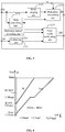
- FIG. 1 shows a switch power supply circuit with feedback control in the prior art.
- the main AC passes through the full-wave rectifier and is converted to high voltage DC and stored in the capacitor C1.
- R2 and C2 provide power to the IC.
- the output voltage is divided by the resistor R6 and R7, then amplified by the amplifier TL431 and transmitted to the voltage sampling terminal of the IC by the optocoupler HI.
- the IC controls the open time and frequency of switchQ1 according to the sampled output voltage and then adjust the energy of the present cycle stored by the primary side winding, so a close loop negative feedback system is formed to maintain the value of the output voltage.
- the work current of optocoupler H1 and TL431 is larger than 1 mA, the standby power consumption of the power system increases.
- Patent Application Us 2010/0208500 is an example of a prior art switching power converter detecting light load conditions and improving light load efficiency.
- a control IC of a switch power supply is provided to decrease the standby power consumption of the power system.
- the control IC of a switch power supply connected with a switch of the switch power supply, comprises: a voltage collecting module, configured to collect a feedback voltage of an output voltage of the switch power supply; an error amplifying module, configured to compare the feedback voltage and a reference voltage and output an error voltage; a time collecting module, configured to obtain a degaussing time signal according to the feedback voltage; and a control module, configured to collect a peak current feedback signal of the switch, control a frequency and duty ratio of a control signal according to the error voltage, the degaussing time signal and the peak current feedback signal, and control the switch according to the control signal, wherein the control module comprises: a collecting unit, configured to collect the peak current feedback signal of the switch;; a mode judging unit, configured to modulate a value of a judging current according to the error voltage, wherein the mode judging unit is a third
- switch power supply comprises a control IC mentioned above; an input filter and rectification module, configured to remove an unwanted frequency from an alternating current (AC) voltage and convert the alternating current (AC) voltage to a direct current (DC) voltage; a switch; a primary side winding, configured to convert the DC voltage to an electromagnetic signal under a control of the switch; a power supply module, configured to provide a voltage to the control IC; a primary side feedback module, configured to divide the voltage of the power supply module and feedback the divided voltage to the control IC; a primary side collecting module, configured to collect the peak current feedback signal of the switch; a secondary side winding, configured to convert the electromagnetic signal to an electric signal and generate an output AC voltage; an output rectification module, configured to convert the output AC voltage to a DC voltage; a voltage regulating module, configured to store the DC voltage from the output rectification module and provide an output power to maintain the value of the output voltage when the switch is closed; and a
- the error amplifying module compares the feedback voltage and a reference voltage and output an error voltage, the load situation of the power system may be judged.
- the frequency and duty ratio of the control signal is controlled according to the load situation of the power system, the degaussing time signal and the peak current feedback signal, to make the power system output a constant voltage and current signal, and the work frequency of a control IC may be reduced when in the low load situation. Therefore, the switch loss of the power system is reduced and then the standby power consumption of the power system decreases.
- a control IC of a switch power supply is provided.
- the control IC is connected to a switch of the switch power supply and comprises: a voltage collecting module 112, configured to collect a feedback voltage of an output voltage of the switch power supply; an error amplifying module 113, configured to compare the feedback voltage and a reference voltage and output an error voltage; a time collecting module 114, configured to obtain a degaussing time signal according to the feedback voltage; and a control module 115, configured to collect a peak current feedback signal of the switch, control a frequency and duty ratio of a control signal according to the error voltage, the degaussing time signal and the peak current feedback signal, and control the switch according to the control signal.
- the degaussing time signal Tds is obtained according to the feedback voltage, and the feedback voltage is relative to the output voltage of the switch power supply.
- an auxiliary winding of the switch power supply couple a primary side winding of the switch power supply and the obtained feedback voltage is a minus voltage.
- the output voltage of a secondary side winding of the switch power supply is the output voltage of the switch power supply, and the auxiliary winding couple the secondary side winding and the obtained feedback voltage is a plus voltage.
- the feedback voltage is an oscillation voltage. So when the voltage collecting module collects the feedback voltage, the degaussing time signal is obtained. The value of the degaussing signal is equal to the turn on time of the diode.
- the error amplifying module compares the feedback voltage and a reference voltage and output an error voltage, the load situation of the power system may be judged.
- the frequency and duty ratio of the control signal is controlled according to the load situation of the power system, the degaussing time signal and the peak current feedback signal to make the power system output a constant voltage and current signal, and the work frequency of a control IC may be reduced when in the low load situation. Therefore, the switch loss of the power system is reduced and then the standby power consumption of the power system decreases.
- VDD is the power terminal
- GND is the ground
- COMP is the compensation terminal
- CS is the collecting terminal of the peak current feedback signal
- INV is the collecting terminal of the feedback voltage
- DRI is the driving terminal to drive the switch.
- control IC further comprises a compensating module 116, configured to compensate the feedback voltage according to the error voltage. Different voltage compensation may be achieved. The heavier is the load, the larger is the voltage compensation, which is to compensate the loss voltage that is loss in the wire.
- the control IC further comprises a circuit starting module 111, configured to output an enable signal when the voltage of the circuit starting module reaches a preset start voltage and provide power to the voltage collecting module, error amplifying module, time collecting module and control module; wherein the control module further configured to receive the enable signal and output the control signal.
- the circuit starting module 111 resets the other module of the control IC.
- the circuit starting module outputs the enable signal and the control IC starts to work and output the control signal, and the switch starts to work according to the control signal at the same time.
- control IC further comprises a high voltage to low voltage converting module 117, configured to provide power and a enable signal to the low voltage part of the control IC according to the output voltage of the power supply module and a reference and bias module 118, configured to provide a reference voltage and a bias voltage.
- the control module 115 comprises: a collecting unit 1151, configured to collect the peak current feedback signal of the switch of the switch power supply; a mode judging unit 1152, configured to modulate the value of a judging current according to the error voltage of the error amplifying module; a mode controlling unit 1153, configured to modulate the value of a controlling current according to the error voltage of the error amplifying module; a reference current providing unit 1154, configured to provide a preset reference current; a pulse width modulating unit 1155, configured to obtain a first comparison voltage VOCP by overlapping the output current of the mode controlling unit and the preset reference current of the reference current providing unit, and output a turn-off pulse OFF for the control signal when the first comparison voltage VOCP is equal to the value of the peak current feedback signal VCS; and a frequency modulating unit 1156, configured to output a turn-on pulse ON for the control signal according to the output current of the mode judging unit, the output current of the mode controlling unit and the degauss
- the control IC When the pulse width modulating unit 1155 operates pulse width modulation, the control IC enters in the PWM mode; when the frequency modulating unit 1156 operates pulse frequency modulation, the control IC enters in the PFM mode; when the pulse width modulating unit 1155 operates pulse width modulation and the frequency modulating unit 1156 operates pulse frequency modulation simultaneously, the control IC enters in the BURST mode.
- the feedback voltage collected by the voltage collecting module 112 is far less than the reference voltage, and the error amplifying module 113 outputs a high level, that is the value of the output voltage VEA of the error amplifying module 113 is VDD.
- the mode judging unit 1152 maintains the judging current and output the judging current to the frequency modulating unit 1156, the mode controlling unit 1153 outputs a maximum current of the controlling current to the pulse width modulating unit 1155 and stops outputting current to the frequency modulating unit 1156 to maintain the peak current feedback signal.
- the peek current Ip of the primary side winding is maintained and Tds/T is maintained.
- Iout 0 . 5 ⁇ NP NS ⁇ Tds T ⁇ Ip
- NP is the number of turns of the primary side winding
- NS is the number of turns of the secondary side winding
- the output current lout of the switch power supply is maintained.
- the frequency modulating unit 1156 modulates the work cycle of the control IC, that is, modulates the work frequency fosc, so Tds/T is maintained. So when the output current of the switch power supply is maintained, the control IC enters in the PFM mode.
- the value feedback voltage gradually approaches the reference voltage and the error voltage VEA decreases gradually from VDD.
- VEA ⁇ V 1 the work situation of the pulse width modulating unit 1155 and the frequency modulating unit 1156 is modulated according to the value of the error voltage VEA, and the pulse width modulating unit 1155 operates pulse width modulation and the frequency modulating unit 1156 operates pulse frequency modulation simultaneously, according to negative feedback voltage, the output voltage of the switch power supply is maintained; when the error voltage VEA decreases to V2, the control IC is adjusted to reach a limit, then if the load decreases further, the output voltage of the switch power supply may increase and the error voltage VEA decrease further; when VEA ⁇ V4, the mode judging unit 1153 modulates the judging current and the control IC enter in the BURST mode.
- FIG. 4 illustrates a schematic diagram of the change trend of the IC work frequency and primary side winding current corresponding to the load according to one exemplary embodiment of the present invention.
- the control IC works under the BURST mode.
- the control IC works under the PWM mode and PFM mode.
- the control IC works under the PWM mode and PFM mode, with the load decrease from heavy to light, the control IC works under PFM mode, then works under PWM mode and then works under the PWM mode and PFM mode.
- the above mentioned work procedure satisfies the requirement of the dynamic characteristic and decreases the work frequency when the load is light, so the work efficiency may be increased.
- the peek current of the primary side winding IP may be maintained the minimum value, the value of the work frequency is changed to a half of the minimum work frequency when the control IC work under the PFM mode, the loss of the switch power supply and the loss of a fake is decreased, so the loss of the switch power supply with no load may be decreased.
- the mode controlling unit 1153 comprises a first current source, connected with the pulse width modulating unit 1155, configured to increase a value of a first output current I1 when the error voltage increases; and a second current source, connected with the frequency modulating unit 1156, configured to decrease a value of a second output current I2 when the error voltage decreases, stop outputting the second output current when the error voltage is equal to the first preset voltage and maintain the value of the second output current when the error voltage is less than a second preset voltage.
- the reference current providing unit is a constant current source and the output voltage of the constant current source is 10.
- the pulse width modulating unit 1155 comprises a resistor R0, a first capacitor C0 and a first comparator A1, one terminal of the resistor R0 is connected to an output terminal of the first current source, an output terminal of the reference current providing unit, an terminal of the capacitor C0 and an negative terminal of the comparator A1, the other terminal of the resistor R0 is connected to the other terminal of the first capacitor C0 and the ground, an positive terminal of the comparator A1 is connected to the collecting unit.
- the first current is controlled by the error voltage, accordingly, when the error reaches the maximum value, the first current reaches the maximum value and the error voltage reaches the maximum value, and the primary peak current Ip obtained according to the peak current feedback signal is maintained.
- the turn-on time of the switch is from receiving the turn-on pulse ON for the control signal to receiving the turn-off pulse OFF for the control signal.
- the primary peak current Ip When the primary peak current Ip is maintained, the time for the first comparator to output the turn-off pulse OFF is constant, so the turn-on duty ratio of the switch is maintained.
- the output voltage of the switch power supply increases, and the error voltage VEA decreases from VDD.
- the first current I1 decreases with the decrease of the error voltage VEA, and the turn-on duty ratio decreases with the decrease of the first current I1, so the output voltage of the switch power supply decreases and a negative feedback is formed.
- the load of the switch power supply become heavy but is not the full load, with the increase of the load, the output voltage of the switch power supply decreases and the error voltage VEA increases.
- the first current I1 increases with the increase of the error voltage VEA, and the turn-on duty ratio increases with the increase of the first current I1, so the output voltage of the switch power supply increases and the output voltage of the switch power supply is maintained to a constant voltage.
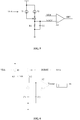
- FIG. 6 illustrates a schematic diagram method of a PFM/BURST mode according to one exemplary embodiment of the present invention.
- the mode judging unit 1152 is a third current source.
- the third current source may reduce the value of a third output current I3 to less than a preset reference current value when the error voltage of the error amplifying module is less than the second preset voltage, and maintain the value of the third output current I3 when the error voltage is equal to or larger than the second preset voltage.
- the frequency modulating unit 1156 comprises: a second capacitor C1; a third capacitor C2; a second comparator A2; a first switch K1, of which a first terminal is connected to the output terminal of the second current source and a second terminal is connected to a terminal of the second capacitor C1 and a negative terminal of the second comparator A2, configured to close or open according to the degaussing time signal; and a second switch K2, of which a first terminal is connected to the output terminal of the second current source, a second terminal is connected to a second terminal of the first switch K1, and a third terminal is connected to a terminal of the third capacitor C2 and a positive terminal of the second comparator A2, configured to connect the first terminal and the second terminal of the second switch or to connect the first terminal and the third terminal of the second switch according to the degaussing time signal.
- the procedure of the PFM/BURST mode comprises four stages: The first stage: in the beginning of the first cycle T, the second capacitor C1 and the third capacitor C2 are reset.
- the second stage receiving the turn-on pulse ON for the control signal VCOMP, the switch is switched on and the degaussing time signal Tds is low level, the third current source may charge the third capacitor C2 through the third output current 13, the voltage of the third capacitor VC2 increases and the second comparator A2 output the high level.
- the third stage a time Ton is ended, the switch is switched off and the procedure may enter the degaussing stage.
- the degaussing time signal Tds is high level, the second output current I2 and the third output current I3 charge the second capacitor C1 together, so the voltage of the second capacitor VC1 increase and the voltage of the third capacitor VC2 is maintained.
- the second comparator A2 turns to low level from high level.
- the fourth stage the degaussing stage is ended, when VC1>VC2, the second comparator A2 outputs low level and the degaussing time signal Tds is low level, the voltage of the second capacitor VC1 is maintained and the third output current I3 charges the third capacitor C2 continuously until VC2>VC1.
- the second comparator A2 turns to high level from low level and the control signal VCOMP turns to low level from high level and output the turn-on pulse ON, the switch is switched on, and resets the second capacitor C1 and the third capacitor C2.
- the first cycle is ended.
- the output voltage of the switch power supply increases, and the error voltage VEA decreases from VDD.
- the second current I2 increases with the decrease of the error voltage VEA.
- the work cycle T increases make the work frequency fosc of the control IC decreases, and the output energy of the switch power supply decreases and the output voltage of the switch power supply decrease; if the load become heavy, the error voltage decreases.
- the second current I2 decreases with the increase of the error voltage, and the work frequency fosc of the control IC is increased. So the output voltage of the switch power supply increases and the negative feedback loop is formed to output a constant voltage.
- the control IC When VEA ⁇ V4, the control IC enters in the BURST mode, the second current I2 is maintained, the value of the third current I3 will jump to a small value and be maintained. According to formula (4), the value of Tds/T may increase further, the work frequency fosc of the control IC decreases further until the control IC jump out of the BURST mode.
- the switch power supply is light load or no load, the work frequency fosc of the control IC is decreased further, so switch consumption of the switch power supply decreases and the purpose of decreasing the standby power consumption is achieved.
- a switch power supply comprising: a control IC mentioned above; an input filter and rectification module 11, configured to remove an unwanted frequency from an alternating current (AC) voltage and convert the alternating current (AC) voltage to a direct current (DC) voltage; a switch; a primary side winding 13, configured to convert the DC voltage to a electromagnetic signal under the control of the switch; a power supply module 14, configured to provide a voltage to the control IC; a primary side feedback module 15, configured to divide the voltage of the power supply module and feedback the divided voltage to the control IC; a primary side collecting module16, configured to collect the peak current feedback signal of the switch; a secondary side winding 17, configured to convert the electromagnetic signal to a electric signal and generate an output AC voltage; an output rectification module 18, configured to convert the output AC voltage to a DC voltage; a voltage regulating module 19, configured to store the DC voltage from the output rectification module and provide an output power to maintain the value of the output voltage when the switch is closed; and a dummy load module
- the error amplifying module compares the feedback voltage and a reference voltage and output an error voltage, the load situation of the power system may be judged.
- the frequency and duty ratio of the control signal is controlled according to the load situation of the power system, the degaussing time signal and the peak current feedback signal to make the power system output a constant voltage and current signal, and the work frequency of a control IC may be reduced when in the low load situation. Therefore, the switch loss of the power system is reduced and then the standby power consumption of the power system decreases.
- the switch power supply further comprises a first voltage absorbing module 21, connected between the input filter and rectification module and the primary side winding and configured to absorb a peak voltage caused by a leakage inductance to avoid breaking the switch.
- the switch power supply further comprises a second voltage absorbing module 22, connected between the secondary side winding and the voltage regulating module and configured to absorb a peak voltage generated during a reverse recovery stage of the output rectification module.
- the primary side of the switch power supply comprises a primary side winding Np, a switch Qlconfigured to control the primary side winding Np and the control IC1 configured to control the switch Q1 to turn on or turn off.
- the switch power supply further comprises a fuse FR1 configured to cute off the AC input to protect the switch power supply when a fault appears.
- the input filter and rectification module comprises a full wave rectifier and a filter.
- the full wave rectifier comprises diodes D1-D4, configured to convert the alternating current (AC) voltage to a direct current (DC) voltage.
- the filter comprises capacitors C01, C02 and inductance L1 configured to remove the unwanted frequency from the AC voltage.
- the power supply module comprises resistors R3, R4, and capacitor C4, auxiliary winding Nd and a diode D6.
- the capacitor C4 is charged through R3and R4 and provides the power to the control IC1.
- the switch power supply starts normally, the primary side winding Np starts to store energy until the primary current reaches a certain value.
- the switch Q1 is switched off when the primary current reaches a certain value.
- the output voltage by the auxiliary winding Nd is divided by R6 and R7 and the divided voltage is feedback to the control IC1, and the control IC1 sample the voltage of R9 and obtains the peak current feedback signal, so the load situation of the switch power supply may be judged and the work status of the switch may be adjusted.
- the switch Q1 is switched off, the energy of Np couples to the output winding Ns, the AC output voltage of Ns is rectified by the output rectification module to a DC voltage.
- the output rectification module is a diode D7.
- the DC voltage output by D7 is stored by the capacitor C7 and provides output voltage when the switch is switched off to maintain the stability of the output voltage.
- the dummy load module is resistor R12 configured to consume energy the output winding Ns to maintain the value of the output voltage.
Landscapes
- Engineering & Computer Science (AREA)
- Power Engineering (AREA)
- Dc-Dc Converters (AREA)
Description
- Example embodiments of the present disclosure relate generally to an IC, and more particularly, to a control IC of a switch power supply and a switch power supply using the same.
- Almost all the main power supply of the household appliance or the power supply for the control part of the household appliance need to use a low voltage direct current (DC) power supply, but considering the voltage transmission loss problem, only 220V or 110V alternating current (AC) power supply can be provided. Therefore, a high efficiency and cost-effective AC-DC converter is indispensable. The traditional AC-DC device is achieved by using a linear converter. But with the disadvantage of huge volume, heavy weight, low convert efficiency and unobvious cost advantage, the linear converter is being eliminated. And the switch power supply becomes a mainstream in the AC-DC devices. To satisfy the accuracy and the isolation safety requirement, a switch power supply with secondary feedback control is generally used.
-
FIG. 1 shows a switch power supply circuit with feedback control in the prior art. The main AC passes through the full-wave rectifier and is converted to high voltage DC and stored in the capacitor C1. R2 and C2 provide power to the IC. The output voltage is divided by the resistor R6 and R7, then amplified by the amplifier TL431 and transmitted to the voltage sampling terminal of the IC by the optocoupler HI. The IC controls the open time and frequency of switchQ1 according to the sampled output voltage and then adjust the energy of the present cycle stored by the primary side winding, so a close loop negative feedback system is formed to maintain the value of the output voltage. But the work current of optocoupler H1 and TL431 is larger than 1 mA, the standby power consumption of the power system increases. - Patent Application Us
2010/0208500 is an example of a prior art switching power converter detecting light load conditions and improving light load efficiency. - According to one exemplary embodiment of the present invention, a control IC of a switch power supply is provided to decrease the standby power consumption of the power system. The control IC of a switch power supply, connected with a switch of the switch power supply, comprises: a voltage collecting module, configured to collect a feedback voltage of an output voltage of the switch power supply; an error amplifying module, configured to compare the feedback voltage and a reference voltage and output an error voltage; a time collecting module, configured to obtain a degaussing time signal according to the feedback voltage; and a control module, configured to collect a peak current feedback signal of the switch, control a frequency and duty ratio of a control signal according to the error voltage, the degaussing time signal and the peak current feedback signal, and control the switch according to the control signal, wherein the control module comprises: a collecting unit, configured to collect the peak current feedback signal of the switch;; a mode judging unit, configured to modulate a value of a judging current according to the error voltage, wherein the mode judging unit is a third current source and is configured to reduce a value of a third output current to less than a preset reference current value when the error voltage is less than the second preset voltage, and maintain the value of the third output current when the error voltage is equal to or larger than the second preset voltage;; a mode controlling unit, configured to modulate a value of a controlling current according to the error voltage, wherein the mode controlling unit comprises: a first current source, connected with the pulse width modulating unit and configured to increase a value of a first output current when the error voltage increases;;; and a second current source, connected with the frequency modulating unit and configured to decrease a value of a second output current when the error voltage decreases, stop outputting the second output current when the error voltage is equal to a first preset voltage and maintain the value of the second output current when the error voltage is less than a second preset voltage;; a reference current providing unit, configured to provide a preset reference current;; a pulse width modulating unit, configured to obtain a first comparison voltage by overlapping an output current of the mode controlling unit and the preset reference current, and output a turn-off pulse for the control signal when the first comparison voltage is equal to the value of the peak current feedback signal;; and a frequency modulating unit, configured to output a turn-on pulse for the control signal according to an output current of the mode judging unit, the output current of the mode controlling unit and the degaussing time signal, wherein the frequency modulating unit comprises: a second capacitor;;; a third capacitor;;; a second comparator;;; a first switch, of which a first terminal is connected to an output terminal of the second current source and a second terminal is connected to a terminal of the second capacitor and a negative terminal of the second comparator, configured to close or open according to the degaussing time signal;;; and a second switch, of which a first terminal is connected to an output terminal of the second current source, a second terminal is connected to a second terminal of the first switch, and a third terminal is connected to a terminal of the third capacitor and a positive terminal of the second comparator, configured to connect the first terminal and the second terminal of the second switch or to connect the first terminal and the third terminal of the second switch according to the degaussing time signal.
- According to one exemplary embodiment of the present invention, switch power supply is also provided. The switch power supply comprises a control IC mentioned above; an input filter and rectification module, configured to remove an unwanted frequency from an alternating current (AC) voltage and convert the alternating current (AC) voltage to a direct current (DC) voltage; a switch; a primary side winding, configured to convert the DC voltage to an electromagnetic signal under a control of the switch; a power supply module, configured to provide a voltage to the control IC; a primary side feedback module, configured to divide the voltage of the power supply module and feedback the divided voltage to the control IC; a primary side collecting module, configured to collect the peak current feedback signal of the switch; a secondary side winding, configured to convert the electromagnetic signal to an electric signal and generate an output AC voltage; an output rectification module, configured to convert the output AC voltage to a DC voltage; a voltage regulating module, configured to store the DC voltage from the output rectification module and provide an output power to maintain the value of the output voltage when the switch is closed; and a dummy load module, configured to consume the output AC voltage from the secondary side winding in no-load situation.
- The error amplifying module compares the feedback voltage and a reference voltage and output an error voltage, the load situation of the power system may be judged. The frequency and duty ratio of the control signal is controlled according to the load situation of the power system, the degaussing time signal and the peak current feedback signal, to make the power system output a constant voltage and current signal, and the work frequency of a control IC may be reduced when in the low load situation. Therefore, the switch loss of the power system is reduced and then the standby power consumption of the power system decreases.
- Having thus described example embodiments of the present disclosure in general terms, reference will now be made to the accompanying drawings, which are not necessarily drawn to scale, and wherein:
-
FIG. 1 illustrates a circuit of a switch power supply in the prior art; -
FIG. 2 illustrates a block diagram of a switch power supply according to one exemplary embodiment of the present invention; -
FIG. 3 illustrates a block diagram of a control module according to one exemplary embodiment of the present invention; -
FIG. 4 illustrates a schematic diagram of the change trend of the IC work frequency and primary side winding current corresponding to the load according to one exemplary embodiment of the present invention; -
FIG. 5 illustrates a schematic diagram method of a PWM mode according to one exemplary embodiment of the present invention; -
FIG. 6 illustrates a schematic diagram method of a PFM/BURST mode according to one exemplary embodiment of the present invention; -
FIG. 7 illustrates a word process diagram of a control module in PFM/BURST mode according to one exemplary embodiment of the present invention; -
FIG. 8 illustrates a circuit of a switch power supply according to one exemplary embodiment of the present invention; and -
FIG. 9 illustrates a circuit of a switch power supply according to one exemplary embodiment of the present invention. - The present invention now will be described more fully hereinafter with reference to the accompanying drawings, in which preferred embodiments of the invention are shown. This invention may, however, be embodied in many different forms and should not be construed as limited to the embodiments set forth herein; rather, these embodiments are provided so that this disclosure will be thorough and complete, and will fully convey the scope of the invention to those skilled in the art.
- Referring to
FIG. 2 , a control IC of a switch power supply is provided. The control IC is connected to a switch of the switch power supply and comprises: avoltage collecting module 112, configured to collect a feedback voltage of an output voltage of the switch power supply; an error amplifyingmodule 113, configured to compare the feedback voltage and a reference voltage and output an error voltage; atime collecting module 114, configured to obtain a degaussing time signal according to the feedback voltage; and acontrol module 115, configured to collect a peak current feedback signal of the switch, control a frequency and duty ratio of a control signal according to the error voltage, the degaussing time signal and the peak current feedback signal, and control the switch according to the control signal. - The degaussing time signal Tds is obtained according to the feedback voltage, and the feedback voltage is relative to the output voltage of the switch power supply. When the switch of the switch power supply is switched on, an auxiliary winding of the switch power supply couple a primary side winding of the switch power supply and the obtained feedback voltage is a minus voltage. When the switch is switched off and a diode of the switch power supply is switched on, the output voltage of a secondary side winding of the switch power supply is the output voltage of the switch power supply, and the auxiliary winding couple the secondary side winding and the obtained feedback voltage is a plus voltage. When the switch is switched off and a diode is switched off, the feedback voltage is an oscillation voltage. So when the voltage collecting module collects the feedback voltage, the degaussing time signal is obtained. The value of the degaussing signal is equal to the turn on time of the diode.
- The error amplifying module compares the feedback voltage and a reference voltage and output an error voltage, the load situation of the power system may be judged. The frequency and duty ratio of the control signal is controlled according to the load situation of the power system, the degaussing time signal and the peak current feedback signal to make the power system output a constant voltage and current signal, and the work frequency of a control IC may be reduced when in the low load situation. Therefore, the switch loss of the power system is reduced and then the standby power consumption of the power system decreases.
- Referring to
FIG. 2 , VDD is the power terminal, GND is the ground, COMP is the compensation terminal, CS is the collecting terminal of the peak current feedback signal, INV is the collecting terminal of the feedback voltage, DRI is the driving terminal to drive the switch. - In some embodiment of the present invention, the control IC further comprises a compensating
module 116, configured to compensate the feedback voltage according to the error voltage. Different voltage compensation may be achieved. The heavier is the load, the larger is the voltage compensation, which is to compensate the loss voltage that is loss in the wire. - In some embodiment of the present invention, the control IC further comprises a
circuit starting module 111, configured to output an enable signal when the voltage of the circuit starting module reaches a preset start voltage and provide power to the voltage collecting module, error amplifying module, time collecting module and control module; wherein the control module further configured to receive the enable signal and output the control signal. When the control IC powers on, thecircuit starting module 111 resets the other module of the control IC. When the voltage of the power supply module reaches the preset start voltage, the circuit starting module outputs the enable signal and the control IC starts to work and output the control signal, and the switch starts to work according to the control signal at the same time. - In some embodiment of the present invention, the control IC further comprises a high voltage to low
voltage converting module 117, configured to provide power and a enable signal to the low voltage part of the control IC according to the output voltage of the power supply module and a reference andbias module 118, configured to provide a reference voltage and a bias voltage. - Referring to
FIG. 3 , thecontrol module 115 comprises: acollecting unit 1151, configured to collect the peak current feedback signal of the switch of the switch power supply; amode judging unit 1152, configured to modulate the value of a judging current according to the error voltage of the error amplifying module; amode controlling unit 1153, configured to modulate the value of a controlling current according to the error voltage of the error amplifying module; a referencecurrent providing unit 1154, configured to provide a preset reference current; a pulsewidth modulating unit 1155, configured to obtain a first comparison voltage VOCP by overlapping the output current of the mode controlling unit and the preset reference current of the reference current providing unit, and output a turn-off pulse OFF for the control signal when the first comparison voltage VOCP is equal to the value of the peak current feedback signal VCS; and a frequency modulatingunit 1156, configured to output a turn-on pulse ON for the control signal according to the output current of the mode judging unit, the output current of the mode controlling unit and the degaussing time signal Tds. - When the pulse
width modulating unit 1155 operates pulse width modulation, the control IC enters in the PWM mode; when the frequency modulatingunit 1156 operates pulse frequency modulation, the control IC enters in the PFM mode; when the pulsewidth modulating unit 1155 operates pulse width modulation and the frequency modulatingunit 1156 operates pulse frequency modulation simultaneously, the control IC enters in the BURST mode. - The output power of the switch power supply is constant, according to the formula P=UI, when the load connected the switch power supply is large, the output current I of the switch power supply increases and the output voltage U of the switch power supply deceases. The feedback voltage collected by the
voltage collecting module 112 is far less than the reference voltage, and the error amplifyingmodule 113 outputs a high level, that is the value of the output voltage VEA of the error amplifyingmodule 113 is VDD. Themode judging unit 1152 maintains the judging current and output the judging current to the frequency modulatingunit 1156, themode controlling unit 1153 outputs a maximum current of the controlling current to the pulsewidth modulating unit 1155 and stops outputting current to the frequency modulatingunit 1156 to maintain the peak current feedback signal. Then the peek current Ip of the primary side winding is maintained and Tds/T is maintained. According to the formula
frequency modulating unit 1156 modulates the work cycle of the control IC, that is, modulates the work frequency fosc, so Tds/T is maintained. So when the output current of the switch power supply is maintained, the control IC enters in the PFM mode. - With the decrease of the load, the value feedback voltage gradually approaches the reference voltage and the error voltage VEA decreases gradually from VDD. When VEA<
V 1, the work situation of the pulsewidth modulating unit 1155 and thefrequency modulating unit 1156 is modulated according to the value of the error voltage VEA, and the pulsewidth modulating unit 1155 operates pulse width modulation and thefrequency modulating unit 1156 operates pulse frequency modulation simultaneously, according to negative feedback voltage, the output voltage of the switch power supply is maintained; when the error voltage VEA decreases to V2, the control IC is adjusted to reach a limit, then if the load decreases further, the output voltage of the switch power supply may increase and the error voltage VEA decrease further; when VEA<V4, themode judging unit 1153 modulates the judging current and the control IC enter in the BURST mode. When the control IC works under the BURST mode, the control IC process frequency division on the basis of the minimum work frequency, if the load increases, the output voltage of the switch power supply decreases, then the error voltage VEA increase; when VEA>V3, the control IC jump out of the BURST mode. There is a delay between V2 and V3. The V1, V2, V3 and V4 decrease successively. -
FIG. 4 illustrates a schematic diagram of the change trend of the IC work frequency and primary side winding current corresponding to the load according to one exemplary embodiment of the present invention. Referring to the shadow part, the control IC works under the BURST mode. In this part of the diagram, the control IC works under the PWM mode and PFM mode. When the control IC works under the PWM mode and PFM mode, with the load decrease from heavy to light, the control IC works under PFM mode, then works under PWM mode and then works under the PWM mode and PFM mode. The above mentioned work procedure satisfies the requirement of the dynamic characteristic and decreases the work frequency when the load is light, so the work efficiency may be increased. In the BURST mode, the peek current of the primary side winding IP may be maintained the minimum value, the value of the work frequency is changed to a half of the minimum work frequency when the control IC work under the PFM mode, the loss of the switch power supply and the loss of a fake is decreased, so the loss of the switch power supply with no load may be decreased. - Referring to
FIG. 5 and FIG. 6 , themode controlling unit 1153 comprises a first current source, connected with the pulsewidth modulating unit 1155, configured to increase a value of a first output current I1 when the error voltage increases; and a second current source, connected with thefrequency modulating unit 1156, configured to decrease a value of a second output current I2 when the error voltage decreases, stop outputting the second output current when the error voltage is equal to the first preset voltage and maintain the value of the second output current when the error voltage is less than a second preset voltage. When the value of the first reset voltage is VDD, that is when VEA=VDD, 12=0, when the error voltage is less than V4, I2 is maintained. - In
FIG. 5 , the reference current providing unit is a constant current source and the output voltage of the constant current source is 10. The pulsewidth modulating unit 1155 comprises a resistor R0, a first capacitor C0 and a first comparator A1, one terminal of the resistor R0 is connected to an output terminal of the first current source, an output terminal of the reference current providing unit, an terminal of the capacitor C0 and an negative terminal of the comparator A1, the other terminal of the resistor R0 is connected to the other terminal of the first capacitor C0 and the ground, an positive terminal of the comparator A1 is connected to the collecting unit. The positive terminal of the comparator A1 is connected to the collecting unit to collect a peak current feedback signal VCS, the negative terminal of the comparator receives a first comparison voltage VOCP, VOCP=RO×(I0+I1). - When the switch power supply is full load or over load, the output voltage of the switch power supply is small, so the collected feedback voltage is small and the error voltage VEA=VDD. The first current is controlled by the error voltage, accordingly, when the error reaches the maximum value, the first current reaches the maximum value and the error voltage reaches the maximum value, and the primary peak current Ip obtained according to the peak current feedback signal is maintained. The turn-on time of the switch is from receiving the turn-on pulse ON for the control signal to receiving the turn-off pulse OFF for the control signal. When the primary peak current Ip is maintained, the time for the first comparator to output the turn-off pulse OFF is constant, so the turn-on duty ratio of the switch is maintained.
- When the load of the switch supply decreases to a preset value, the output voltage of the switch power supply increases, and the error voltage VEA decreases from VDD. The first current I1 decreases with the decrease of the error voltage VEA, and the turn-on duty ratio decreases with the decrease of the first current I1, so the output voltage of the switch power supply decreases and a negative feedback is formed. If the load of the switch power supply become heavy but is not the full load, with the increase of the load, the output voltage of the switch power supply decreases and the error voltage VEA increases. The first current I1 increases with the increase of the error voltage VEA, and the turn-on duty ratio increases with the increase of the first current I1, so the output voltage of the switch power supply increases and the output voltage of the switch power supply is maintained to a constant voltage.
-
FIG. 6 illustrates a schematic diagram method of a PFM/BURST mode according to one exemplary embodiment of the present invention. In some embodiments of the present invention, themode judging unit 1152 is a third current source. The third current source may reduce the value of a third output current I3 to less than a preset reference current value when the error voltage of the error amplifying module is less than the second preset voltage, and maintain the value of the third output current I3 when the error voltage is equal to or larger than the second preset voltage. - The
frequency modulating unit 1156 comprises: a second capacitor C1; a third capacitor C2; a second comparator A2; a first switch K1, of which a first terminal is connected to the output terminal of the second current source and a second terminal is connected to a terminal of the second capacitor C1 and a negative terminal of the second comparator A2, configured to close or open according to the degaussing time signal; and a second switch K2, of which a first terminal is connected to the output terminal of the second current source, a second terminal is connected to a second terminal of the first switch K1, and a third terminal is connected to a terminal of the third capacitor C2 and a positive terminal of the second comparator A2, configured to connect the first terminal and the second terminal of the second switch or to connect the first terminal and the third terminal of the second switch according to the degaussing time signal. - Referring to
FIG. 7 , in some embodiment of the present invention, the procedure of the PFM/BURST mode comprises four stages:
The first stage: in the beginning of the first cycle T, the second capacitor C1 and the third capacitor C2 are reset. - The second stage: receiving the turn-on pulse ON for the control signal VCOMP, the switch is switched on and the degaussing time signal Tds is low level, the third current source may charge the third capacitor C2 through the third output current 13, the voltage of the third capacitor VC2 increases and the second comparator A2 output the high level.
- The third stage: a time Ton is ended, the switch is switched off and the procedure may enter the degaussing stage. The degaussing time signal Tds is high level, the second output current I2 and the third output current I3 charge the second capacitor C1 together, so the voltage of the second capacitor VC1 increase and the voltage of the third capacitor VC2 is maintained. When VC1>VC2, the second comparator A2 turns to low level from high level.
- The fourth stage: the degaussing stage is ended, when VC1>VC2, the second comparator A2 outputs low level and the degaussing time signal Tds is low level, the voltage of the second capacitor VC1 is maintained and the third output current I3 charges the third capacitor C2 continuously until VC2>VC1. When VC2>VC1, the second comparator A2 turns to high level from low level and the control signal VCOMP turns to low level from high level and output the turn-on pulse ON, the switch is switched on, and resets the second capacitor C1 and the third capacitor C2. The first cycle is ended.
- According to the work procedure mentioned above, some formulas described below are obtained:


- The formula

- When the switch power supply is full load or over load, the output voltage of the switch power supply is small, so the collected feedback voltage is small and the error voltage VEA=VDD. When VEA=VDD, 12=0, the change of the second current is opposite to the change of VEA, the third current I3 is maintain, so the charge current for the second capacitor C1 and the third capacitor C2 is the same, the formula

- When the load of the switch supply decreases to a preset value, the output voltage of the switch power supply increases, and the error voltage VEA decreases from VDD. The second current I2 increases with the decrease of the error voltage VEA. According to formula (4), the work cycle T increases make the work frequency fosc of the control IC decreases, and the output energy of the switch power supply decreases and the output voltage of the switch power supply decrease; if the load become heavy, the error voltage decreases. The second current I2 decreases with the increase of the error voltage, and the work frequency fosc of the control IC is increased. So the output voltage of the switch power supply increases and the negative feedback loop is formed to output a constant voltage.
- When V2<VEA<V1, the control IC enters in the PWM and PFM mode, the second current I2 is changed with the error voltage VEA. The smaller is the error voltage VEA, the larger is the second current 12. According to formula (4), Tds/T decreases with the decrease of the error voltage VEA, if Tds is maintained, the work cycle T increases with the decrease of the error voltage VEA. That is with the decrease of the error voltage VEA, the work frequency fosc of the control IC is decreased, the purpose of the PFM is achieved.
- When VEA<V4, the control IC enters in the BURST mode, the second current I2 is maintained, the value of the third current I3 will jump to a small value and be maintained. According to formula (4), the value of Tds/T may increase further, the work frequency fosc of the control IC decreases further until the control IC jump out of the BURST mode. When VEA<V4, it may be known the switch power supply is light load or no load, the work frequency fosc of the control IC is decreased further, so switch consumption of the switch power supply decreases and the purpose of decreasing the standby power consumption is achieved.
- Referring to
FIG. 8 , a switch power supply comprising: a control IC mentioned above; an input filter andrectification module 11, configured to remove an unwanted frequency from an alternating current (AC) voltage and convert the alternating current (AC) voltage to a direct current (DC) voltage; a switch; a primary side winding 13, configured to convert the DC voltage to a electromagnetic signal under the control of the switch; apower supply module 14, configured to provide a voltage to the control IC; a primaryside feedback module 15, configured to divide the voltage of the power supply module and feedback the divided voltage to the control IC; a primary side collecting module16, configured to collect the peak current feedback signal of the switch; a secondary side winding 17, configured to convert the electromagnetic signal to a electric signal and generate an output AC voltage; anoutput rectification module 18, configured to convert the output AC voltage to a DC voltage; avoltage regulating module 19, configured to store the DC voltage from the output rectification module and provide an output power to maintain the value of the output voltage when the switch is closed; and adummy load module 20, configured to consume the output AC voltage from the secondary side winding in no-load situation. - The error amplifying module compares the feedback voltage and a reference voltage and output an error voltage, the load situation of the power system may be judged. The frequency and duty ratio of the control signal is controlled according to the load situation of the power system, the degaussing time signal and the peak current feedback signal to make the power system output a constant voltage and current signal, and the work frequency of a control IC may be reduced when in the low load situation. Therefore, the switch loss of the power system is reduced and then the standby power consumption of the power system decreases.
- In some embodiment of the present invention, the switch power supply further comprises a first
voltage absorbing module 21, connected between the input filter and rectification module and the primary side winding and configured to absorb a peak voltage caused by a leakage inductance to avoid breaking the switch. - In some embodiment of the present invention, the switch power supply further comprises a second
voltage absorbing module 22, connected between the secondary side winding and the voltage regulating module and configured to absorb a peak voltage generated during a reverse recovery stage of the output rectification module. - Referring to
FIG. 9 , the primary side of the switch power supply comprises a primary side winding Np, a switch Qlconfigured to control the primary side winding Np and the control IC1 configured to control the switch Q1 to turn on or turn off. The switch power supply further comprises a fuse FR1 configured to cute off the AC input to protect the switch power supply when a fault appears. The input filter and rectification module comprises a full wave rectifier and a filter. The full wave rectifier comprises diodes D1-D4, configured to convert the alternating current (AC) voltage to a direct current (DC) voltage. The filter comprises capacitors C01, C02 and inductance L1 configured to remove the unwanted frequency from the AC voltage. The power supply module comprises resistors R3, R4, and capacitor C4, auxiliary winding Nd and a diode D6. The capacitor C4 is charged through R3and R4 and provides the power to the control IC1. When the voltage of the control IC1 reaches a preset start voltage, the switch power supply starts normally, the primary side winding Np starts to store energy until the primary current reaches a certain value. The switch Q1 is switched off when the primary current reaches a certain value. The output voltage by the auxiliary winding Nd is divided by R6 and R7 and the divided voltage is feedback to the control IC1, and the control IC1 sample the voltage of R9 and obtains the peak current feedback signal, so the load situation of the switch power supply may be judged and the work status of the switch may be adjusted. When the switch Q1 is switched off, the energy of Np couples to the output winding Ns, the AC output voltage of Ns is rectified by the output rectification module to a DC voltage. In this embodiment, the output rectification module is a diode D7. The DC voltage output by D7 is stored by the capacitor C7 and provides output voltage when the switch is switched off to maintain the stability of the output voltage. In this embodiment, the dummy load module is resistor R12 configured to consume energy the output winding Ns to maintain the value of the output voltage.
Claims (9)
- A control IC of a switch power supply, connected with a switch of the switch power supply, comprising:a voltage collecting module (112), configured to collect a feedback voltage of an output voltage of the switch power supply;an error amplifying module (113), configured to compare the feedback voltage and a reference voltage and output an error voltage;a time collecting module (114), configured to obtain a degaussing time signal according to the feedback voltage; anda control module (115), configured to collect a peak current feedback signal of the switch, control a frequency and duty ratio of a control signal according to the error voltage (VEA), the degaussing time signal (Tds) and the peak current feedback signal (CS), and control the switch according to the control signal, wherein the control module (115) comprises:a collecting unit (1151), configured to collect the peak current feedback signal (CS) of the switch;a mode judging unit (1152), configured to modulate a value of a judging current according to the error voltage (VEA), wherein the mode judging unit (1152) is a third current source and is configured to reduce a value of a third output current to less than a preset reference current value when the error voltage (VEA) is less than the second preset voltage, and maintain the value of the third output current when the error voltage (VEA) is equal to or larger than the second preset voltage;a mode controlling unit (1153), configured to modulate a value of a controlling current according to the error voltage (VEA), wherein the mode controlling unit (1153) comprises:a first current source, connected with the pulse width modulating unit (1155) and configured to increase a value of a first output current (II) when the error voltage (VEA) increases; anda second current source, connected with the frequency modulating unit (1156) and configured to decrease a value of a second output current (12) when the error voltage (VEA) decreases, stop outputting the second output current when the error voltage (VEA) is equal to a first preset voltage and maintain the value of the second output current when the error voltage (VEA) is less than a second preset voltage;a reference current providing unit (1154), configured to provide a preset reference current;a pulse width modulating unit (1155), configured to obtain a first comparison voltage by overlapping an output current of the mode controlling unit (1153) and the preset reference current, and output a turn-off pulse for the control signal when the first comparison voltage is equal to the value of the peak current feedback signal (CS); anda frequency modulating unit (1156), configured to output a turn-on pulse (ON) for the control signal according to an output current of the mode judging unit (1152), the output current of the mode controlling unit (1153) and the degaussing time signal (Tds), wherein the frequency modulating unit (1156) comprises:a second capacitor;a third capacitor;a second comparator;a first switch, of which a first terminal is connected to an output terminal of the second current source and a second terminal is connected to a terminal of the second capacitor and a negative terminal of the second comparator, configured to close or open according to the degaussing time signal (Tds); anda second switch, of which a first terminal is connected to an output terminal of the second current source, a second terminal is connected to a second terminal of the first switch, and a third terminal is connected to a terminal of the third capacitor and a positive terminal of the second comparator, configured to connect the first terminal and the second terminal of the second switch or to connect the first terminal and the third terminal of the second switch according to the degaussing time signal.
- The control IC of a switch power supply of claim 1, wherein the reference current providing unit is a constant current source.
- The control IC of a switch power supply of claim 1, wherein the pulse width modulating unit (1155) comprises a resistor, a first capacitor and a first comparator, one terminal of the resistor is connected to an output terminal of the first current source, an output terminal of the reference current providing unit (1154), an terminal of the capacitor and an negative terminal of the comparator, the other terminal of the resister is connected to the other terminal of the capacitor and is grounded respectively, a positive terminal of the comparator is connected to the collecting unit.
- The control IC of a switch power supply of anyone of claims 1 to 3, further comprising:
a circuit starting module (111), configured to output an enable signal when a voltage of the circuit starting module (111) reaches a preset start voltage. - The control IC of a switch power supply of claim 4, wherein the control module (115) is further configured to output the control signal when receiving the enable signal.
- The control IC of a switch power supply of anyone of claims 1 to 5, further comprising a compensating module (116), configured to compensate the feedback voltage according to the error voltage (VEA).
- A switch power supply, comprising:a control IC of any of claims 1-10;an input filter and rectification module (11), configured to remove an unwanted frequency from an alternating current (AC) voltage and convert the alternating current (AC) voltage to a direct current (DC) voltage;a switch;a primary side winding (13), configured to convert the DC voltage to an electromagnetic signal under a control of the switch;a power supply module (14), configured to provide a voltage to the control IC;a primary side feedback module (15), configured to divide the voltage of the power supply module (14) and feedback the divided voltage to the control IC;a primary side collecting module (16), configured to collect the peak current feedback signal of the switch;a secondary side winding (17), configured to convert the electromagnetic signal to an electric signal and generate an output AC voltage;an output rectification module (18), configured to convert the output AC voltage to a DC voltage;a voltage regulating module (19), configured to store the DC voltage from the output rectification module (18) and provide an output power to maintain the value of the output voltage when the switch is closed; anda dummy load module (20), configured to consume the output AC voltage from the secondary side winding (17) in no-load situation.
- The switch power supply of claim 7, further comprising:
a first voltage absorbing module (21), connected between the input filter and rectification module (11) and the primary side winding (13) and configured to absorb a peak voltage caused by a leakage inductance. - The switch power supply of claim 7 or 8, further comprising:
a second voltage absorbing module (22), connected between the secondary side winding (17) and the voltage regulating module (19) and configured to absorb a peak voltage generated during a reverse recovery stage of the output rectification module (18).
Applications Claiming Priority (2)
| Application Number | Priority Date | Filing Date | Title |
|---|---|---|---|
| CN201110215457.0A CN102904448B (en) | 2011-07-29 | 2011-07-29 | Control chip of switch power supply and switch power supply |
| PCT/CN2012/079294 WO2013017050A1 (en) | 2011-07-29 | 2012-07-27 | A control ic of a switch power supply and a switch power supply using the same |
Publications (3)
| Publication Number | Publication Date |
|---|---|
| EP2737617A1 EP2737617A1 (en) | 2014-06-04 |
| EP2737617A4 EP2737617A4 (en) | 2015-05-06 |
| EP2737617B1 true EP2737617B1 (en) | 2018-06-13 |
Family
ID=47576538
Family Applications (1)
| Application Number | Title | Priority Date | Filing Date |
|---|---|---|---|
| EP12819890.0A Active EP2737617B1 (en) | 2011-07-29 | 2012-07-27 | A control ic of a switch power supply and a switch power supply using the same |
Country Status (4)
| Country | Link |
|---|---|
| US (1) | US8976546B2 (en) |
| EP (1) | EP2737617B1 (en) |
| CN (1) | CN102904448B (en) |
| WO (1) | WO2013017050A1 (en) |
Families Citing this family (42)
| Publication number | Priority date | Publication date | Assignee | Title |
|---|---|---|---|---|
| CN102904448B (en) | 2011-07-29 | 2015-07-22 | 比亚迪股份有限公司 | Control chip of switch power supply and switch power supply |
| CN103490636B (en) * | 2012-06-11 | 2016-06-22 | 比亚迪股份有限公司 | For the quasi-resonance control method of Switching Power Supply, system and device |
| CN104038082B (en) * | 2013-03-04 | 2017-12-12 | 比亚迪股份有限公司 | Switching Power Supply, the control method of Switching Power Supply and control chip |
| CN103200738B (en) * | 2013-03-29 | 2015-11-25 | 深圳市明微电子股份有限公司 | A kind of constant current driving governor and constant current driver circuit for LED |
| US9124101B2 (en) * | 2013-04-02 | 2015-09-01 | Bel Fuse (Macao Commercial Offshore) Limited | Power supply having selectable operation based on communications with load |
| CN103166450B (en) | 2013-04-15 | 2015-08-26 | 矽力杰半导体技术(杭州)有限公司 | Voltage transmission loss compensating circuit, compensation method, control chip and Switching Power Supply |
| US9337726B2 (en) * | 2013-08-27 | 2016-05-10 | Intersil Americas LLC | PWM/PFM controller for use with switched-mode power supply |
| CN104422808B (en) * | 2013-08-30 | 2017-09-29 | 比亚迪股份有限公司 | A kind of sample circuit, switching power source control circuit, Switching Power Supply and the method for sampling |
| CN104578792B (en) * | 2013-10-17 | 2017-11-28 | 比亚迪股份有限公司 | Line loss compensation device, switch power supply system and line loss compensation method |
| CN104734510B (en) * | 2013-12-20 | 2017-05-03 | 比亚迪股份有限公司 | Switch power supply and control chip thereof |
| US9310817B2 (en) | 2014-02-04 | 2016-04-12 | Synaptics Incorporated | Negative voltage feedback generator |
| US9941798B2 (en) | 2014-02-14 | 2018-04-10 | Infineon Technologies Austria Ag | Switched-mode power conversion |
| CN103929855B (en) * | 2014-04-02 | 2017-01-25 | 深圳市明微电子股份有限公司 | LED lighting device, LED driving circuit and switch power source driving chip of LED driving circuit |
| CN105226971B (en) * | 2015-11-10 | 2019-05-21 | 昂宝电子(上海)有限公司 | Method and system for adjusting peak frequency with duty cycle |
| US9968720B2 (en) | 2016-04-11 | 2018-05-15 | CorWave SA | Implantable pump system having an undulating membrane |
| US10166319B2 (en) | 2016-04-11 | 2019-01-01 | CorWave SA | Implantable pump system having a coaxial ventricular cannula |
| CN107659149B (en) * | 2016-12-08 | 2023-08-29 | 深圳市华芯邦科技有限公司 | Hybrid DC power conversion device and method |
| CN108270357B (en) * | 2016-12-30 | 2020-03-31 | 比亚迪股份有限公司 | Switching power supply and its feedforward compensation circuit |
| US10298137B2 (en) * | 2017-03-10 | 2019-05-21 | Semiconductor Components Industries, Llc | Advanced frequency reduction of quasi-resonant converters |
| AU2018242620B2 (en) | 2017-03-31 | 2023-11-16 | CorWave SA | Implantable pump system having a rectangular membrane |
| FR3073578B1 (en) | 2017-11-10 | 2019-12-13 | Corwave | FLUID CIRCULATOR WITH RINGING MEMBRANE |
| US10188779B1 (en) | 2017-11-29 | 2019-01-29 | CorWave SA | Implantable pump system having an undulating membrane with improved hydraulic performance |
| CN108183602B (en) * | 2017-12-26 | 2020-04-21 | 深圳市群芯科创电子有限公司 | Starting circuit |
| JP2019193324A (en) * | 2018-04-18 | 2019-10-31 | オンキヨー株式会社 | Switching power supply |
| CN109039112B (en) * | 2018-07-06 | 2024-05-17 | 富满微电子集团股份有限公司 | Primary side feedback switching power supply control chip, control system and charger |
| US12551689B2 (en) | 2018-12-05 | 2026-02-17 | CorWave SA | Apparatus and methods for coupling a blood pump to the heart |
| US10799625B2 (en) | 2019-03-15 | 2020-10-13 | CorWave SA | Systems and methods for controlling an implantable blood pump |
| CN112019034B (en) * | 2019-05-31 | 2024-07-05 | 广东美的制冷设备有限公司 | Drive control method, device, household appliance and computer readable storage medium |
| CN110190735B (en) * | 2019-06-21 | 2025-01-07 | 杰华特微电子股份有限公司 | Switching Power Supply |
| CN110995002B (en) * | 2019-11-14 | 2021-09-28 | 深圳市稳先微电子有限公司 | Constant-voltage loop control circuit and method, switching power supply control circuit and chip |
| WO2021176423A1 (en) | 2020-03-06 | 2021-09-10 | CorWave SA | Implantable blood pumps comprising a linear bearing |
| CN112564489B (en) * | 2020-11-03 | 2022-05-20 | 广州金升阳科技有限公司 | Mode control method of switch converter and switch converter |
| CN112838772B (en) * | 2021-01-18 | 2022-05-13 | 昂宝电子(上海)有限公司 | Flyback switching power supply and control method thereof |
| US12567810B2 (en) * | 2021-05-13 | 2026-03-03 | Chengdu Monolithic Power Systems Co., Ltd. | Circuit for controlling a switching mode power supply and the method thereof |
| CN113098243B (en) * | 2021-05-13 | 2022-09-06 | 成都芯源系统有限公司 | Control circuit of switching power supply and control method thereof |
| US12251550B2 (en) | 2022-04-26 | 2025-03-18 | CorWave SA | Blood pumps having an encapsulated actuator |
| CN115333335B (en) * | 2022-08-30 | 2025-06-27 | 浪潮(山东)计算机科技有限公司 | A dummy load and control circuit, high voltage switching power supply |
| CN120282816A (en) | 2022-11-15 | 2025-07-08 | 科瓦韦公司 | Implantable cardiac pump system including improved apex connector and/or implant connector |
| US12257427B2 (en) | 2022-11-15 | 2025-03-25 | CorWave SA | Implantable heart pump systems including an improved apical connector and/or graft connector |
| CN116131577B (en) * | 2023-02-16 | 2023-10-17 | 西安致芯微电子有限公司 | Sampling control system, method, controller and primary side feedback AC/DC converter |
| CN118631070B (en) * | 2024-08-12 | 2024-11-12 | 广东省大湾区集成电路与系统应用研究院 | Push-pull power supply circuit and driver chip |
| CN119382489A (en) * | 2025-01-02 | 2025-01-28 | 成都华兴大地科技有限公司 | An active clamp lossless absorption circuit for synchronous rectification of switching power supply |
Family Cites Families (27)
| Publication number | Priority date | Publication date | Assignee | Title |
|---|---|---|---|---|
| JP3883826B2 (en) | 2001-07-18 | 2007-02-21 | ソニー株式会社 | Switching power supply |
| JP4033855B2 (en) * | 2004-11-02 | 2008-01-16 | 松下電器産業株式会社 | Switching power supply control semiconductor device and switching power supply device using the same |
| JP4682647B2 (en) * | 2005-03-07 | 2011-05-11 | サンケン電気株式会社 | Switching power supply |
| WO2007003967A2 (en) * | 2005-07-06 | 2007-01-11 | Cambridge Semiconductor Limited | Switch mode power supply control systems |
| JP2007295761A (en) * | 2006-04-27 | 2007-11-08 | Matsushita Electric Ind Co Ltd | Switching power supply |
| CN200969527Y (en) | 2006-09-30 | 2007-10-31 | Bcd半导体制造有限公司 | Charger circuit and its charger |
| JP2008187813A (en) * | 2007-01-30 | 2008-08-14 | Fuji Electric Device Technology Co Ltd | Switching power supply |
| JP5056055B2 (en) * | 2007-02-19 | 2012-10-24 | 富士電機株式会社 | Integrated circuit for switching power supply control and switching power supply device |
| US7974107B2 (en) * | 2007-08-28 | 2011-07-05 | Iwatt Inc. | System and method for controlling a current limit with primary side sensing using a hybrid PWM and PFM control |
| US7859864B2 (en) * | 2007-11-28 | 2010-12-28 | Fuji Electric Systems Co., Ltd. | Switching power supply device |
| US8125799B2 (en) * | 2009-10-23 | 2012-02-28 | Bcd Semiconductor Manufacturing Limited | Control circuits and methods for switching mode power supplies |
| JP5353119B2 (en) * | 2008-08-26 | 2013-11-27 | サンケン電気株式会社 | Switching power supply |
| CN101677214B (en) * | 2008-09-17 | 2012-06-06 | 比亚迪股份有限公司 | Switching mode power source |
| US8289732B2 (en) * | 2008-12-23 | 2012-10-16 | Iwatt Inc. | Controller for switching power converter driving BJT based on primary side adaptive digital control |
| US8199537B2 (en) * | 2009-02-19 | 2012-06-12 | Iwatt Inc. | Detecting light load conditions and improving light load efficiency in a switching power converter |
| US8018743B2 (en) * | 2009-03-05 | 2011-09-13 | Iwatt Inc. | Adaptive control for transition between multiple modulation modes in a switching power converter |
| CN101577481B (en) * | 2009-03-27 | 2012-06-27 | Bcd半导体制造有限公司 | Zero-current start circuit and method of switch power supply |
| US8045348B2 (en) * | 2009-04-09 | 2011-10-25 | Bcd Semiconductor Manufacturing Limited | Switching mode power supply controller with high voltage startup circuits |
| CN201430530Y (en) | 2009-06-09 | 2010-03-24 | 瑞谷科技(深圳)有限公司 | Step-down converting circuit |
| JP2010288334A (en) * | 2009-06-09 | 2010-12-24 | Panasonic Corp | Switching power supply device and semiconductor device |
| CN201540530U (en) * | 2009-11-06 | 2010-08-04 | 深圳市福瑞康电子有限公司 | Power adapter applicable to laptop |
| CN102497107B (en) * | 2011-12-09 | 2015-04-01 | 上海新进半导体制造有限公司 | Switch power supply and controller of switch power supply |
| CN101841247B (en) * | 2009-11-20 | 2013-01-23 | Bcd半导体制造有限公司 | Base drive circuit of switching power supply |
| CN101860243B (en) * | 2010-05-14 | 2012-12-19 | 西安英洛华微电子有限公司 | Line loss compensation circuit for switch power supply |
| CN101924471B (en) * | 2010-08-31 | 2013-05-01 | 深圳市明微电子股份有限公司 | Method for constantly outputting current and device thereof |
| JP2012161117A (en) * | 2011-01-28 | 2012-08-23 | Rohm Co Ltd | Dc/dc converter, and power supply device and electronic apparatus using the same |
| CN102904448B (en) | 2011-07-29 | 2015-07-22 | 比亚迪股份有限公司 | Control chip of switch power supply and switch power supply |
-
2011
- 2011-07-29 CN CN201110215457.0A patent/CN102904448B/en active Active
-
2012
- 2012-07-27 WO PCT/CN2012/079294 patent/WO2013017050A1/en not_active Ceased
- 2012-07-27 EP EP12819890.0A patent/EP2737617B1/en active Active
- 2012-07-30 US US13/561,354 patent/US8976546B2/en active Active
Non-Patent Citations (1)
| Title |
|---|
| None * |
Also Published As
| Publication number | Publication date |
|---|---|
| EP2737617A4 (en) | 2015-05-06 |
| US8976546B2 (en) | 2015-03-10 |
| WO2013017050A1 (en) | 2013-02-07 |
| CN102904448B (en) | 2015-07-22 |
| EP2737617A1 (en) | 2014-06-04 |
| CN102904448A (en) | 2013-01-30 |
| US20130027985A1 (en) | 2013-01-31 |
Similar Documents
| Publication | Publication Date | Title |
|---|---|---|
| EP2737617A1 (en) | A control ic of a switch power supply and a switch power supply using the same | |
| US7965523B2 (en) | Switching power supply device | |
| US10770979B2 (en) | LLC resonant converter | |
| US9190917B2 (en) | Isolated flyback converter for light emitting diode driver | |
| EP2416477B1 (en) | AD-DC converter and control circuit thereof | |
| EP2720365B1 (en) | Bi-directional DC/DC converter | |
| US8837174B2 (en) | Switching power-supply apparatus including switching elements having a low threshold voltage | |
| US9866108B2 (en) | PFC shutdown circuit for light load | |
| US9667153B2 (en) | Switching power supply apparatus for generating control signal for lowering switching frequency of switching devices | |
| US6469913B2 (en) | Switching power supply device having series capacitance | |
| US9647566B2 (en) | Switching power supply apparatus | |
| CN102792574B (en) | Switching power supply device | |
| US9312774B2 (en) | Switch control method, switch controller, and converter comprising the switch controller | |
| EP2367274A2 (en) | Switching mode power supply with primary side control and the method thereof | |
| CN108352787A (en) | Flyback converter | |
| US20130308349A1 (en) | Switching regulator, the control circuit and the method thereof | |
| CN104158400A (en) | Modularized high-pressure power supply circuit | |
| KR102136564B1 (en) | Power supply apparatus and driving method thereof | |
| CN109687702B (en) | DC-DC converter | |
| US20130010501A1 (en) | Bisynchronous resonant switching-type direct current power supply | |
| CN102545627A (en) | Constant current power supply device | |
| CN203352469U (en) | Power Converter, Current Limiting Unit and Control Circuit | |
| US9966861B1 (en) | Active clamp converter and control method for the same | |
| US11356029B2 (en) | Rectifying circuit and switched-mode power supply incorporating rectifying circuit | |
| US12155312B2 (en) | Power converter controller, power converter and method for operating control of a power stage based on an intermediate voltage with respect to a threshold value determined from a turns ratio of a transformer |
Legal Events
| Date | Code | Title | Description |
|---|---|---|---|
| PUAI | Public reference made under article 153(3) epc to a published international application that has entered the european phase |
Free format text: ORIGINAL CODE: 0009012 |
|
| 17P | Request for examination filed |
Effective date: 20140221 |
|
| AK | Designated contracting states |
Kind code of ref document: A1 Designated state(s): AL AT BE BG CH CY CZ DE DK EE ES FI FR GB GR HR HU IE IS IT LI LT LU LV MC MK MT NL NO PL PT RO RS SE SI SK SM TR |
|
| DAX | Request for extension of the european patent (deleted) | ||
| RA4 | Supplementary search report drawn up and despatched (corrected) |
Effective date: 20150407 |
|
| RIC1 | Information provided on ipc code assigned before grant |
Ipc: H02M 7/217 20060101AFI20150330BHEP Ipc: H02M 3/335 20060101ALI20150330BHEP |
|
| GRAP | Despatch of communication of intention to grant a patent |
Free format text: ORIGINAL CODE: EPIDOSNIGR1 |
|
| STAA | Information on the status of an ep patent application or granted ep patent |
Free format text: STATUS: GRANT OF PATENT IS INTENDED |
|
| RIC1 | Information provided on ipc code assigned before grant |
Ipc: H02M 3/335 20060101ALI20171127BHEP Ipc: H02M 7/217 20060101AFI20171127BHEP |
|
| INTG | Intention to grant announced |
Effective date: 20180102 |
|
| GRAS | Grant fee paid |
Free format text: ORIGINAL CODE: EPIDOSNIGR3 |
|
| GRAA | (expected) grant |
Free format text: ORIGINAL CODE: 0009210 |
|
| STAA | Information on the status of an ep patent application or granted ep patent |
Free format text: STATUS: THE PATENT HAS BEEN GRANTED |
|
| AK | Designated contracting states |
Kind code of ref document: B1 Designated state(s): AL AT BE BG CH CY CZ DE DK EE ES FI FR GB GR HR HU IE IS IT LI LT LU LV MC MK MT NL NO PL PT RO RS SE SI SK SM TR |
|
| REG | Reference to a national code |
Ref country code: GB Ref legal event code: FG4D |
|
| REG | Reference to a national code |
Ref country code: CH Ref legal event code: EP Ref country code: AT Ref legal event code: REF Ref document number: 1009509 Country of ref document: AT Kind code of ref document: T Effective date: 20180615 |
|
| REG | Reference to a national code |
Ref country code: IE Ref legal event code: FG4D |
|
| REG | Reference to a national code |
Ref country code: DE Ref legal event code: R096 Ref document number: 602012047501 Country of ref document: DE |
|
| REG | Reference to a national code |
Ref country code: FR Ref legal event code: PLFP Year of fee payment: 7 |
|
| REG | Reference to a national code |
Ref country code: NL Ref legal event code: MP Effective date: 20180613 |
|
| REG | Reference to a national code |
Ref country code: LT Ref legal event code: MG4D |
|
| PG25 | Lapsed in a contracting state [announced via postgrant information from national office to epo] |
Ref country code: SE Free format text: LAPSE BECAUSE OF FAILURE TO SUBMIT A TRANSLATION OF THE DESCRIPTION OR TO PAY THE FEE WITHIN THE PRESCRIBED TIME-LIMIT Effective date: 20180613 Ref country code: ES Free format text: LAPSE BECAUSE OF FAILURE TO SUBMIT A TRANSLATION OF THE DESCRIPTION OR TO PAY THE FEE WITHIN THE PRESCRIBED TIME-LIMIT Effective date: 20180613 Ref country code: LT Free format text: LAPSE BECAUSE OF FAILURE TO SUBMIT A TRANSLATION OF THE DESCRIPTION OR TO PAY THE FEE WITHIN THE PRESCRIBED TIME-LIMIT Effective date: 20180613 Ref country code: NO Free format text: LAPSE BECAUSE OF FAILURE TO SUBMIT A TRANSLATION OF THE DESCRIPTION OR TO PAY THE FEE WITHIN THE PRESCRIBED TIME-LIMIT Effective date: 20180913 Ref country code: BG Free format text: LAPSE BECAUSE OF FAILURE TO SUBMIT A TRANSLATION OF THE DESCRIPTION OR TO PAY THE FEE WITHIN THE PRESCRIBED TIME-LIMIT Effective date: 20180913 Ref country code: FI Free format text: LAPSE BECAUSE OF FAILURE TO SUBMIT A TRANSLATION OF THE DESCRIPTION OR TO PAY THE FEE WITHIN THE PRESCRIBED TIME-LIMIT Effective date: 20180613 Ref country code: CY Free format text: LAPSE BECAUSE OF FAILURE TO SUBMIT A TRANSLATION OF THE DESCRIPTION OR TO PAY THE FEE WITHIN THE PRESCRIBED TIME-LIMIT Effective date: 20180613 |
|
| PG25 | Lapsed in a contracting state [announced via postgrant information from national office to epo] |
Ref country code: LV Free format text: LAPSE BECAUSE OF FAILURE TO SUBMIT A TRANSLATION OF THE DESCRIPTION OR TO PAY THE FEE WITHIN THE PRESCRIBED TIME-LIMIT Effective date: 20180613 Ref country code: RS Free format text: LAPSE BECAUSE OF FAILURE TO SUBMIT A TRANSLATION OF THE DESCRIPTION OR TO PAY THE FEE WITHIN THE PRESCRIBED TIME-LIMIT Effective date: 20180613 Ref country code: HR Free format text: LAPSE BECAUSE OF FAILURE TO SUBMIT A TRANSLATION OF THE DESCRIPTION OR TO PAY THE FEE WITHIN THE PRESCRIBED TIME-LIMIT Effective date: 20180613 Ref country code: GR Free format text: LAPSE BECAUSE OF FAILURE TO SUBMIT A TRANSLATION OF THE DESCRIPTION OR TO PAY THE FEE WITHIN THE PRESCRIBED TIME-LIMIT Effective date: 20180914 |
|
| REG | Reference to a national code |
Ref country code: AT Ref legal event code: MK05 Ref document number: 1009509 Country of ref document: AT Kind code of ref document: T Effective date: 20180613 |
|
| PG25 | Lapsed in a contracting state [announced via postgrant information from national office to epo] |
Ref country code: NL Free format text: LAPSE BECAUSE OF FAILURE TO SUBMIT A TRANSLATION OF THE DESCRIPTION OR TO PAY THE FEE WITHIN THE PRESCRIBED TIME-LIMIT Effective date: 20180613 |
|
| PG25 | Lapsed in a contracting state [announced via postgrant information from national office to epo] |
Ref country code: CZ Free format text: LAPSE BECAUSE OF FAILURE TO SUBMIT A TRANSLATION OF THE DESCRIPTION OR TO PAY THE FEE WITHIN THE PRESCRIBED TIME-LIMIT Effective date: 20180613 Ref country code: AT Free format text: LAPSE BECAUSE OF FAILURE TO SUBMIT A TRANSLATION OF THE DESCRIPTION OR TO PAY THE FEE WITHIN THE PRESCRIBED TIME-LIMIT Effective date: 20180613 Ref country code: IS Free format text: LAPSE BECAUSE OF FAILURE TO SUBMIT A TRANSLATION OF THE DESCRIPTION OR TO PAY THE FEE WITHIN THE PRESCRIBED TIME-LIMIT Effective date: 20181013 Ref country code: PL Free format text: LAPSE BECAUSE OF FAILURE TO SUBMIT A TRANSLATION OF THE DESCRIPTION OR TO PAY THE FEE WITHIN THE PRESCRIBED TIME-LIMIT Effective date: 20180613 Ref country code: EE Free format text: LAPSE BECAUSE OF FAILURE TO SUBMIT A TRANSLATION OF THE DESCRIPTION OR TO PAY THE FEE WITHIN THE PRESCRIBED TIME-LIMIT Effective date: 20180613 Ref country code: SK Free format text: LAPSE BECAUSE OF FAILURE TO SUBMIT A TRANSLATION OF THE DESCRIPTION OR TO PAY THE FEE WITHIN THE PRESCRIBED TIME-LIMIT Effective date: 20180613 Ref country code: RO Free format text: LAPSE BECAUSE OF FAILURE TO SUBMIT A TRANSLATION OF THE DESCRIPTION OR TO PAY THE FEE WITHIN THE PRESCRIBED TIME-LIMIT Effective date: 20180613 |
|
| PG25 | Lapsed in a contracting state [announced via postgrant information from national office to epo] |
Ref country code: IT Free format text: LAPSE BECAUSE OF FAILURE TO SUBMIT A TRANSLATION OF THE DESCRIPTION OR TO PAY THE FEE WITHIN THE PRESCRIBED TIME-LIMIT Effective date: 20180613 Ref country code: SM Free format text: LAPSE BECAUSE OF FAILURE TO SUBMIT A TRANSLATION OF THE DESCRIPTION OR TO PAY THE FEE WITHIN THE PRESCRIBED TIME-LIMIT Effective date: 20180613 |
|
| REG | Reference to a national code |
Ref country code: CH Ref legal event code: PL |
|
| REG | Reference to a national code |
Ref country code: DE Ref legal event code: R097 Ref document number: 602012047501 Country of ref document: DE |
|
| PG25 | Lapsed in a contracting state [announced via postgrant information from national office to epo] |
Ref country code: MC Free format text: LAPSE BECAUSE OF FAILURE TO SUBMIT A TRANSLATION OF THE DESCRIPTION OR TO PAY THE FEE WITHIN THE PRESCRIBED TIME-LIMIT Effective date: 20180613 Ref country code: LU Free format text: LAPSE BECAUSE OF NON-PAYMENT OF DUE FEES Effective date: 20180727 |
|
| REG | Reference to a national code |
Ref country code: BE Ref legal event code: MM Effective date: 20180731 |
|
| PLBE | No opposition filed within time limit |
Free format text: ORIGINAL CODE: 0009261 |
|
| STAA | Information on the status of an ep patent application or granted ep patent |
Free format text: STATUS: NO OPPOSITION FILED WITHIN TIME LIMIT |
|
| PG25 | Lapsed in a contracting state [announced via postgrant information from national office to epo] |
Ref country code: CH Free format text: LAPSE BECAUSE OF NON-PAYMENT OF DUE FEES Effective date: 20180731 Ref country code: LI Free format text: LAPSE BECAUSE OF NON-PAYMENT OF DUE FEES Effective date: 20180731 |
|
| REG | Reference to a national code |
Ref country code: IE Ref legal event code: MM4A |
|
| 26N | No opposition filed |
Effective date: 20190314 |
|
| PG25 | Lapsed in a contracting state [announced via postgrant information from national office to epo] |
Ref country code: DK Free format text: LAPSE BECAUSE OF FAILURE TO SUBMIT A TRANSLATION OF THE DESCRIPTION OR TO PAY THE FEE WITHIN THE PRESCRIBED TIME-LIMIT Effective date: 20180613 Ref country code: BE Free format text: LAPSE BECAUSE OF NON-PAYMENT OF DUE FEES Effective date: 20180731 Ref country code: SI Free format text: LAPSE BECAUSE OF FAILURE TO SUBMIT A TRANSLATION OF THE DESCRIPTION OR TO PAY THE FEE WITHIN THE PRESCRIBED TIME-LIMIT Effective date: 20180613 |
|
| PG25 | Lapsed in a contracting state [announced via postgrant information from national office to epo] |
Ref country code: IE Free format text: LAPSE BECAUSE OF NON-PAYMENT OF DUE FEES Effective date: 20180727 |
|
| PG25 | Lapsed in a contracting state [announced via postgrant information from national office to epo] |
Ref country code: AL Free format text: LAPSE BECAUSE OF FAILURE TO SUBMIT A TRANSLATION OF THE DESCRIPTION OR TO PAY THE FEE WITHIN THE PRESCRIBED TIME-LIMIT Effective date: 20180613 |
|
| PG25 | Lapsed in a contracting state [announced via postgrant information from national office to epo] |
Ref country code: MT Free format text: LAPSE BECAUSE OF NON-PAYMENT OF DUE FEES Effective date: 20180727 |
|
| PG25 | Lapsed in a contracting state [announced via postgrant information from national office to epo] |
Ref country code: TR Free format text: LAPSE BECAUSE OF FAILURE TO SUBMIT A TRANSLATION OF THE DESCRIPTION OR TO PAY THE FEE WITHIN THE PRESCRIBED TIME-LIMIT Effective date: 20180613 |
|
| REG | Reference to a national code |
Ref country code: DE Ref legal event code: R081 Ref document number: 602012047501 Country of ref document: DE Owner name: BYD COMPANY LIMITED, SHENZHEN, CN Free format text: FORMER OWNERS: BYD COMPANY LIMITED, SHENZHEN, GUANGDONG, CN; SHENZHEN BYD AUTO R&D COMPANY LIMITED, SHENZHEN, GUANGDONG, CN |
|
| PG25 | Lapsed in a contracting state [announced via postgrant information from national office to epo] |
Ref country code: HU Free format text: LAPSE BECAUSE OF FAILURE TO SUBMIT A TRANSLATION OF THE DESCRIPTION OR TO PAY THE FEE WITHIN THE PRESCRIBED TIME-LIMIT; INVALID AB INITIO Effective date: 20120727 Ref country code: PT Free format text: LAPSE BECAUSE OF FAILURE TO SUBMIT A TRANSLATION OF THE DESCRIPTION OR TO PAY THE FEE WITHIN THE PRESCRIBED TIME-LIMIT Effective date: 20180613 |
|
| PG25 | Lapsed in a contracting state [announced via postgrant information from national office to epo] |
Ref country code: MK Free format text: LAPSE BECAUSE OF NON-PAYMENT OF DUE FEES Effective date: 20180613 |
|
| P01 | Opt-out of the competence of the unified patent court (upc) registered |
Effective date: 20230527 |
|
| PGFP | Annual fee paid to national office [announced via postgrant information from national office to epo] |
Ref country code: DE Payment date: 20250722 Year of fee payment: 14 |
|
| PGFP | Annual fee paid to national office [announced via postgrant information from national office to epo] |
Ref country code: GB Payment date: 20250722 Year of fee payment: 14 |
|
| PGFP | Annual fee paid to national office [announced via postgrant information from national office to epo] |
Ref country code: FR Payment date: 20250725 Year of fee payment: 14 |