EP2736066A2 - Method for manufacturing a superhydrophobic film sheet - Google Patents
Method for manufacturing a superhydrophobic film sheet Download PDFInfo
- Publication number
- EP2736066A2 EP2736066A2 EP12817539.5A EP12817539A EP2736066A2 EP 2736066 A2 EP2736066 A2 EP 2736066A2 EP 12817539 A EP12817539 A EP 12817539A EP 2736066 A2 EP2736066 A2 EP 2736066A2
- Authority
- EP
- European Patent Office
- Prior art keywords
- photoresist
- super
- film sheet
- baking
- soft
- Prior art date
- Legal status (The legal status is an assumption and is not a legal conclusion. Google has not performed a legal analysis and makes no representation as to the accuracy of the status listed.)
- Granted
Links
Images



Classifications
-
- H—ELECTRICITY
- H10—SEMICONDUCTOR DEVICES; ELECTRIC SOLID-STATE DEVICES NOT OTHERWISE PROVIDED FOR
- H10P—GENERIC PROCESSES OR APPARATUS FOR THE MANUFACTURE OR TREATMENT OF DEVICES COVERED BY CLASS H10
- H10P76/00—Manufacture or treatment of masks on semiconductor bodies, e.g. by lithography or photolithography
- H10P76/20—Manufacture or treatment of masks on semiconductor bodies, e.g. by lithography or photolithography of masks comprising organic materials
- H10P76/204—Manufacture or treatment of masks on semiconductor bodies, e.g. by lithography or photolithography of masks comprising organic materials of organic photoresist masks
- H10P76/2041—Photolithographic processes
-
- B—PERFORMING OPERATIONS; TRANSPORTING
- B82—NANOTECHNOLOGY
- B82Y—SPECIFIC USES OR APPLICATIONS OF NANOSTRUCTURES; MEASUREMENT OR ANALYSIS OF NANOSTRUCTURES; MANUFACTURE OR TREATMENT OF NANOSTRUCTURES
- B82Y10/00—Nanotechnology for information processing, storage or transmission, e.g. quantum computing or single electron logic
-
- B—PERFORMING OPERATIONS; TRANSPORTING
- B82—NANOTECHNOLOGY
- B82Y—SPECIFIC USES OR APPLICATIONS OF NANOSTRUCTURES; MEASUREMENT OR ANALYSIS OF NANOSTRUCTURES; MANUFACTURE OR TREATMENT OF NANOSTRUCTURES
- B82Y40/00—Manufacture or treatment of nanostructures
-
- G—PHYSICS
- G03—PHOTOGRAPHY; CINEMATOGRAPHY; ANALOGOUS TECHNIQUES USING WAVES OTHER THAN OPTICAL WAVES; ELECTROGRAPHY; HOLOGRAPHY
- G03F—PHOTOMECHANICAL PRODUCTION OF TEXTURED OR PATTERNED SURFACES, e.g. FOR PRINTING, FOR PROCESSING OF SEMICONDUCTOR DEVICES; MATERIALS THEREFOR; ORIGINALS THEREFOR; APPARATUS SPECIALLY ADAPTED THEREFOR
- G03F7/00—Photomechanical, e.g. photolithographic, production of textured or patterned surfaces, e.g. printing surfaces; Materials therefor, e.g. comprising photoresists; Apparatus specially adapted therefor
-
- G—PHYSICS
- G03—PHOTOGRAPHY; CINEMATOGRAPHY; ANALOGOUS TECHNIQUES USING WAVES OTHER THAN OPTICAL WAVES; ELECTROGRAPHY; HOLOGRAPHY
- G03F—PHOTOMECHANICAL PRODUCTION OF TEXTURED OR PATTERNED SURFACES, e.g. FOR PRINTING, FOR PROCESSING OF SEMICONDUCTOR DEVICES; MATERIALS THEREFOR; ORIGINALS THEREFOR; APPARATUS SPECIALLY ADAPTED THEREFOR
- G03F7/00—Photomechanical, e.g. photolithographic, production of textured or patterned surfaces, e.g. printing surfaces; Materials therefor, e.g. comprising photoresists; Apparatus specially adapted therefor
- G03F7/0002—Lithographic processes using patterning methods other than those involving the exposure to radiation, e.g. by stamping
-
- G—PHYSICS
- G03—PHOTOGRAPHY; CINEMATOGRAPHY; ANALOGOUS TECHNIQUES USING WAVES OTHER THAN OPTICAL WAVES; ELECTROGRAPHY; HOLOGRAPHY
- G03F—PHOTOMECHANICAL PRODUCTION OF TEXTURED OR PATTERNED SURFACES, e.g. FOR PRINTING, FOR PROCESSING OF SEMICONDUCTOR DEVICES; MATERIALS THEREFOR; ORIGINALS THEREFOR; APPARATUS SPECIALLY ADAPTED THEREFOR
- G03F7/00—Photomechanical, e.g. photolithographic, production of textured or patterned surfaces, e.g. printing surfaces; Materials therefor, e.g. comprising photoresists; Apparatus specially adapted therefor
- G03F7/26—Processing photosensitive materials; Apparatus therefor
- G03F7/40—Treatment after imagewise removal, e.g. baking
-
- H—ELECTRICITY
- H10—SEMICONDUCTOR DEVICES; ELECTRIC SOLID-STATE DEVICES NOT OTHERWISE PROVIDED FOR
- H10P—GENERIC PROCESSES OR APPARATUS FOR THE MANUFACTURE OR TREATMENT OF DEVICES COVERED BY CLASS H10
- H10P76/00—Manufacture or treatment of masks on semiconductor bodies, e.g. by lithography or photolithography
- H10P76/20—Manufacture or treatment of masks on semiconductor bodies, e.g. by lithography or photolithography of masks comprising organic materials
- H10P76/204—Manufacture or treatment of masks on semiconductor bodies, e.g. by lithography or photolithography of masks comprising organic materials of organic photoresist masks
Landscapes
- Physics & Mathematics (AREA)
- General Physics & Mathematics (AREA)
- Engineering & Computer Science (AREA)
- Nanotechnology (AREA)
- Chemical & Material Sciences (AREA)
- Crystallography & Structural Chemistry (AREA)
- Condensed Matter Physics & Semiconductors (AREA)
- Theoretical Computer Science (AREA)
- Mathematical Physics (AREA)
- Manufacturing & Machinery (AREA)
- Application Of Or Painting With Fluid Materials (AREA)
- Photosensitive Polymer And Photoresist Processing (AREA)
- Shaping Of Tube Ends By Bending Or Straightening (AREA)
- Laminated Bodies (AREA)
- Treatments Of Macromolecular Shaped Articles (AREA)
- Casting Or Compression Moulding Of Plastics Or The Like (AREA)
- Manufacture Of Macromolecular Shaped Articles (AREA)
- Exposure Of Semiconductors, Excluding Electron Or Ion Beam Exposure (AREA)
- Materials For Photolithography (AREA)
Abstract
Description
- The invention relates to the method for fabricating super-hydrophobic film sheet, more specifically the method for fabricating super-hydrophobic film sheet with a super-hydrophobic surface comprising creating a structure with protrusion having super-hydrophobic effect like a lotus leaf and coating on it PDMS which is polymer of optically transparent material with hydrophobic property.
- Many studies trying to implement a super-hydrophobic surface have been performed, but most of them are performed by doing chemical treatment of a surface or building a nanostructure through semiconductor processing using a silicon wafer.
- Fabrication method of a pattern with super-hydrophobic surface was disclosed in the Korean Patent Application Publication, No.
10-2010-0008579 - Fabrication method of a pattern with super-hydrophobic surface according to the prior art comprise, as disclosed in the Publication, (a) forming micro-lens array with a plurality of micro-lenses uniformly arranged using photolithography process; and (b) forming micro-bowl array with a plurality of micro-bowls of complementary shape to the micro-lens uniformly arranged, using the micro-lens array as a mold.
- However, making the pattern by using conventional semiconductor process, such as etching process etc., as described in the prior art has the problem that a series of processes from applying to removing photoresist has to be repeated at least more than three times.
- Reference 1: Korean Patent Application Publication, No.
10-2010-0008579 (Jan. 16, 2010 - The invention is therefore directed to solving the above mentioned problem. The object of the invention is to provide a method for fabricating super-hydrophobic film sheet with a super-hydrophobic surface, comprising creating a structure with protrusion having super-hydrophobic effect like a lotus leaf by controlling the period of time and the number of times for baking photoresist; and coating on it PDMS which is polymer of optically transparent material with hydrophobic property.
- This object is according to a first aspect of the invention achieved by a method for fabrication of super-hydrophobic film sheet, comprising the steps of: (a) cleaning a surface of a silicon wafer; (b) coating the surface of the silicon wafer with photoresist(photo sensitizer)(AZ4620) using a spin coater, then soft-baking it; (c) exposing the structure made by step(b) using a mask aligner; (d) developing using photoresist developer(AZ400K); (e) perform PDMS molding over the upper side of the structure made by the step (d); and (f) removing the photoresist(AZ4620) using acetone to complete the super-hydrophobic film sheet with protrusion at the end portion, wherein the soft-baking in the step (b) is performed predetermined times, with different period of curing on each soft-baking, to make the thickness of photoresist higher and to make the end portion of photoresist first cured, wherein PDMS in the step(e) is coated over the upper side of the structure made by the step (d) using the spin coater and soft-baking of PDMS is performed predetermined times using a vacuum oven, with different period of time for curing on each soft-baking, and wherein the inside of the photoresist is not completely cured even after the predetermined times of soft-baking is performed, resulting in the protrusion formed at the end portion by the steps of exposing and developing.
- According to the invention, a super-hydrophobic film sheet with a super-hydrophobic surface could be fabricated by creating a structure with protrusion having super-hydrophobic effect like a lotus leaf and coating on it PDMS which is polymer of optically transparent material with hydrophobic property.
- Also, according to the invention, the time and cost for the fabrication could be reduced by modulating the curing time to be shorter than in the conventional method of fabrication.
- Further, according to the invention, the super-hydrophobic film sheet with a super-hydrophobic like a lotus leaf could be applied to a side mirror of a vehicle. When applied to the side mirror, in case of rain, the super-hydrophobic film sheet could prevent beads of raindrop from being formed on it, thus resulting in self-cleaning effect.
-
-
FIG. 1 shows the flow chart of the method for fabrication of super-hydrophobic film sheet according to the invention; -
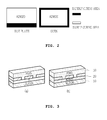
FIG. 2 illustrates the difference in rapidness of curing in a hot plate and an oven; -
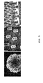
FIG. 3 illustrates a structure built by a conventional fabrication method and a structure built by the fabrication method according to this invention; -
FIG. 4 shows images of protrusion in the super-hydrophobic film sheet by an optical microscope; -
FIG. 5 shows images of protrusion in the super-hydrophobic film sheet by a scanning electron microscope; -
FIG. 6 shows image comparison in case of existence and nonexistence of the protrusion according to this invention. -
- 10: silicon wafer 20: photoresist
- 30: PDMS
- Specific features and advantages will become clearer by the following description, referring to the drawings attached. It is noted that detailed descriptions of well-known devices and their functions related to this invention are omitted so as not to obscure the description of this invention with unnecessary detail.
- Hereinafter detailed descriptions of the invention are set forth, referring to the drawings attached.
- Super-hydrophobic film sheet and the fabrication method thereof according to this invention are explained as follows, referring to the
FIGS. 1 to 6 . -
FIG. 1 shows the flow chart of the method for fabrication of super-hydrophobic film sheet. As showed, the surface of a silicon wafer is cleaned (S10). - Here the surface of the silicon wafer may be cleaned using Pirana, RCA1, RCA2, etc.
- Then the top of the silicon wafer (10) is coated with photoresist (photo sensitizer) (AZ4620) (20) using a spin coater, and subjected to soft-baking (S20).
- Specifically, the photoresist (AZ4620) (20) is coated at 3000rpm for 3s using the spin coater, and cured in an oven. This coating and baking process is performed three times.
- Here at the first and second time it is cured for 5 min at 90°C in the oven, and at third time for 28 min at 90°C. Thus three times of layer coating leads to 60µm of thickness of the layer (20 µm per one time).
- This soft-baking process may be performed differently using a hot plate or an oven.
- As showed in
FIG. 2 , in case that the process is performed using the hot plate (90°C), the curing is begun from the bottom side due to mechanical properties. However in case of use of the oven (90°C), the curing is begun rapidly from the outer side and the inside is slowly cured. - The fabrication method according to this invention uses the oven in the step (20), and a structure having a shape of protrusion is formed using the properties of being cured in the oven.
- The process using the hot plate (90°C) brings a round shape in the end portion, while the process using the oven results in a protrusion shape because the inside is not completely cured even after three times of baking steps, which influences the exposing step and the developing step.
- Thus, as described in the above, the peculiar structure of protrusion shape can be formed by controlling the period of time and the times of the curing of the photoresist.
- Then the structure made in the step S20 is subjected to exposing using mask aligner (S30) and developed for 25 min using photoresist developer (AZ400K) (S40).
- Subsequently, the upper side of the structure made through the step S40 is molded (S50).
- Specifically, it is coated with PDMS (30), polymer of transparent material, at 1000rpm for 40s using the spin coater, and then is subjected to soft-baking using a vacuum oven. This coating and baking process is performed three times.
- Here at the first and second time it is cured for 15 min in the vacuum oven, and at third time for 2 hours in the vacuum oven.
- The PDMS can be easily introduced inside the structure since vacuum state is maintained by the vacuum oven as stated in the above.
- Finally, the phptoresist (AZ4620) is removed using acetone and the super-hydrophobic film sheet with nanostructure as depicted in
FIG. 3 is completed (S60).FIG. 3(a) shows a structure made by conventional fabrication method. - As illustrated in
FIGS. 4 and5 , the pattern of the super-hydrophobic film sheet has the similar structure to a lotus leaf. Also showed by the optical microscopic image (FIG. 4 ) and the scanning electron microscopic (SEM) image (FIG. 5 ), the protrusion of pine cone shape is formed at the end portion of the structure of 50µm height, bringing a super-hydrophobic effect like the lotus leaf. -
FIG. 6 shows image comparison in case of existence and nonexistence of the protrusion according to this invention.FIG. 6(a) shows the contact angle image in case that no protrusion exists, andFIG. 6(b) the contact angle image in case that the protrusion exists. As illustrated in the drawing, it shows that a superior contact angle could be made and the contact angle of 140° was measured. - While the invention has been described in connection with what is presently considered to be most practical and preferred embodiments, it is to be understood the invention is not to be limited to the disclosed embodiments, but on the contrary, is intended to cover various modifications and equivalents.
Claims (3)
- A method for fabrication of super-hydrophobic film sheet, comprising the steps of:(a) cleaning a surface of a silicon wafer;(b) coating the surface of the silicon wafer with photoresist using a spin coater, then soft-baking it;(c) exposing the structure made by step(b) using a mask aligner;(d) developing using photoresist developer;(e) perform PDMS molding over the upper side of the structure made by the step (d); and(f) removing the photoresist using acetone to complete the super-hydrophobic film sheet with protrusion at the end portion,
wherein the soft-baking in the step (b) is performed predetermined times, with different period of curing on each soft-baking, to make the thickness of photoresist higher and to make the end portion of photoresist first cured,
wherein PDMS in the step (e) is coated over the upper side of the structure made by the step (d) using the spin coater and soft-baking of PDMS is performed predetermined times using a vacuum oven, with different period of time for curing on each soft-baking,
and wherein the inside of the photoresist is not completely cured even after the predetermined times of soft-baking is performed, resulting in the protrusion formed at the end portion by the steps of exposing and developing. - The method for fabrication of super-hydrophobic film sheet of claim 1, wherein the step (a) of cleaning is performed using any one among Pirana, RCA 1 and RCA 2.
- The method for fabrication of super-hydrophobic film sheet of claim 1, the PDMS is introduced into the structure in a vacuum.
Applications Claiming Priority (2)
| Application Number | Priority Date | Filing Date | Title |
|---|---|---|---|
| KR1020110072945A KR101166152B1 (en) | 2011-07-22 | 2011-07-22 | Method for manufacturing super hydrophobic film sheet |
| PCT/KR2012/005774 WO2013015562A2 (en) | 2011-07-22 | 2012-07-19 | Method for manufacturing a superhydrophobic film sheet |
Publications (3)
| Publication Number | Publication Date |
|---|---|
| EP2736066A2 true EP2736066A2 (en) | 2014-05-28 |
| EP2736066A4 EP2736066A4 (en) | 2015-03-18 |
| EP2736066B1 EP2736066B1 (en) | 2018-08-15 |
Family
ID=46716930
Family Applications (1)
| Application Number | Title | Priority Date | Filing Date |
|---|---|---|---|
| EP12817539.5A Not-in-force EP2736066B1 (en) | 2011-07-22 | 2012-07-19 | Method for manufacturing a superhydrophobic film sheet |
Country Status (4)
| Country | Link |
|---|---|
| EP (1) | EP2736066B1 (en) |
| KR (1) | KR101166152B1 (en) |
| CN (1) | CN103814428B (en) |
| WO (1) | WO2013015562A2 (en) |
Cited By (1)
| Publication number | Priority date | Publication date | Assignee | Title |
|---|---|---|---|---|
| EP3932659A4 (en) * | 2019-02-28 | 2023-01-11 | Realook & Company Co., Ltd. | Water repellent film for car side-view mirror, and molding apparatus therefor |
Families Citing this family (4)
| Publication number | Priority date | Publication date | Assignee | Title |
|---|---|---|---|---|
| TWI566941B (en) * | 2015-06-12 | 2017-01-21 | 國立清華大學 | Diversion superhydrophobic structure |
| CN108394858A (en) * | 2018-02-27 | 2018-08-14 | 合肥工业大学 | A kind of production method of PDMS flexibilities based superhydrophobic thin films |
| CN112495734B (en) * | 2020-11-05 | 2023-01-17 | 江苏中新瑞光学材料有限公司 | A kind of production technology of hydrophobic material |
| CN117507199A (en) * | 2023-11-14 | 2024-02-06 | 吉林大学 | A method for local anti-icing on superhydrophobic transparent films |
Family Cites Families (9)
| Publication number | Priority date | Publication date | Assignee | Title |
|---|---|---|---|---|
| JP2005262522A (en) * | 2004-03-17 | 2005-09-29 | Pentax Corp | Production method of polymer sheet |
| US20070231542A1 (en) * | 2006-04-03 | 2007-10-04 | General Electric Company | Articles having low wettability and high light transmission |
| TW200901188A (en) * | 2007-06-22 | 2009-01-01 | Daxon Technology Inc | Method of making an optical disc |
| CN101157767B (en) * | 2007-11-23 | 2010-06-16 | 陈洪 | Super-hydrophobic polystyrene film and preparation method thereof |
| KR100981313B1 (en) * | 2008-07-16 | 2010-09-10 | 한국과학기술원 | Patterns with superhydrophobic and superhydrophobic surfaces and methods for forming the same |
| KR20100037717A (en) * | 2008-10-02 | 2010-04-12 | 연세대학교 산학협력단 | Micropatterning method of thin p3ht films via plasma enhanced polymer transfer printing and manufacturing method of otfts having the p3ht micropatterned thin film as an active layer |
| CN101537682B (en) * | 2009-03-16 | 2011-06-29 | 浙江工业大学 | A method for preparing superhydrophobic surfaces by nanoparticle-assisted micromolding |
| US20120126458A1 (en) * | 2009-05-26 | 2012-05-24 | King William P | Casting microstructures into stiff and durable materials from a flexible and reusable mold |
| US9956743B2 (en) * | 2010-12-20 | 2018-05-01 | The Regents Of The University Of California | Superhydrophobic and superoleophobic nanosurfaces |
-
2011
- 2011-07-22 KR KR1020110072945A patent/KR101166152B1/en active Active
-
2012
- 2012-07-19 WO PCT/KR2012/005774 patent/WO2013015562A2/en not_active Ceased
- 2012-07-19 EP EP12817539.5A patent/EP2736066B1/en not_active Not-in-force
- 2012-07-19 CN CN201280045937.XA patent/CN103814428B/en active Active
Cited By (1)
| Publication number | Priority date | Publication date | Assignee | Title |
|---|---|---|---|---|
| EP3932659A4 (en) * | 2019-02-28 | 2023-01-11 | Realook & Company Co., Ltd. | Water repellent film for car side-view mirror, and molding apparatus therefor |
Also Published As
| Publication number | Publication date |
|---|---|
| EP2736066B1 (en) | 2018-08-15 |
| CN103814428B (en) | 2016-05-11 |
| KR101166152B1 (en) | 2012-07-18 |
| WO2013015562A2 (en) | 2013-01-31 |
| EP2736066A4 (en) | 2015-03-18 |
| CN103814428A (en) | 2014-05-21 |
| WO2013015562A3 (en) | 2013-03-21 |
Similar Documents
| Publication | Publication Date | Title |
|---|---|---|
| US7579136B2 (en) | Microfluidic device and method of manufacturing the same | |
| CA2849381C (en) | Fabrication of free standing membranes and use thereof for synthesis of nanoparticle patterns | |
| EP2736066B1 (en) | Method for manufacturing a superhydrophobic film sheet | |
| CN101688934B (en) | Optical element and method for manufacturing the same | |
| KR100981313B1 (en) | Patterns with superhydrophobic and superhydrophobic surfaces and methods for forming the same | |
| CN103777256A (en) | Manufacturing method and application for flexible curved micro-lens array | |
| CN108109952B (en) | Micro pick-up array and method of manufacturing the same | |
| US9690188B2 (en) | Photomask and method for manufacturing photomask | |
| KR101669734B1 (en) | Superhydrophobic sheet and method of manufacturing the same | |
| JP2007110122A (en) | Method for manufacturing high sag lens, and high sag lens manufactured thereby | |
| TW201430396A (en) | Optical element structure and optical element fabricating process for the same | |
| KR102382260B1 (en) | Method for producing an optical glass element | |
| CN105445825B (en) | Wafer-level method of manufacturing an apertured lens and associated apertured lens system | |
| CN101571604A (en) | Method for producing double-sided lenses | |
| US20220111562A1 (en) | Method for producing a structure having at least one curved pattern | |
| CN112731774A (en) | Method for manufacturing micro-nano optical device | |
| JP5565771B2 (en) | Microlens manufacturing method and imaging device | |
| KR101350403B1 (en) | High numerical aperture lens for using fluoro-polymer thin film coating and manufacturing method thereof | |
| KR20190087028A (en) | Microlens array and method of forming the same | |
| Toukhy et al. | Improved thermal flow characteristic resist optimized for the manufacturing of microlenses | |
| TW202544487A (en) | Manufacturing method and structure of the structure | |
| Wang et al. | Patterning of SU-8 resist with digital micromirror device (DMD) maskless lithography | |
| JP5487671B2 (en) | Pattern formation method | |
| JP2001083303A (en) | Micro lens array and method of manufacturing the same | |
| HK1222711B (en) | Wafer-level methods for making apertured lenses and associated apertured lens systems |
Legal Events
| Date | Code | Title | Description |
|---|---|---|---|
| PUAI | Public reference made under article 153(3) epc to a published international application that has entered the european phase |
Free format text: ORIGINAL CODE: 0009012 |
|
| 17P | Request for examination filed |
Effective date: 20140219 |
|
| AK | Designated contracting states |
Kind code of ref document: A2 Designated state(s): AL AT BE BG CH CY CZ DE DK EE ES FI FR GB GR HR HU IE IS IT LI LT LU LV MC MK MT NL NO PL PT RO RS SE SI SK SM TR |
|
| RIN1 | Information on inventor provided before grant (corrected) |
Inventor name: PARK, SEUNG HWAN Inventor name: LEE, SA MYUNG Inventor name: PARK, JONG SUNG Inventor name: GO, GUN Inventor name: LEE, DONG WEON |
|
| DAX | Request for extension of the european patent (deleted) | ||
| A4 | Supplementary search report drawn up and despatched |
Effective date: 20150218 |
|
| RIC1 | Information provided on ipc code assigned before grant |
Ipc: G03F 7/00 20060101ALI20150212BHEP Ipc: G03F 7/40 20060101ALI20150212BHEP Ipc: H01L 21/027 20060101AFI20150212BHEP |
|
| RIN1 | Information on inventor provided before grant (corrected) |
Inventor name: LEE, SA MYUNG Inventor name: PARK, JONG SUNG Inventor name: GO, GUN Inventor name: PARK, SEUNG HWAN Inventor name: LEE, DONG WEON |
|
| REG | Reference to a national code |
Ref country code: DE Ref legal event code: R079 Ref document number: 602012049897 Country of ref document: DE Free format text: PREVIOUS MAIN CLASS: H01L0021027000 Ipc: G03F0007000000 |
|
| RIC1 | Information provided on ipc code assigned before grant |
Ipc: H01L 21/027 20060101ALI20180301BHEP Ipc: B82Y 40/00 20110101ALI20180301BHEP Ipc: G03F 7/40 20060101ALI20180301BHEP Ipc: G03F 7/00 20060101AFI20180301BHEP Ipc: B82Y 10/00 20110101ALI20180301BHEP |
|
| GRAP | Despatch of communication of intention to grant a patent |
Free format text: ORIGINAL CODE: EPIDOSNIGR1 |
|
| STAA | Information on the status of an ep patent application or granted ep patent |
Free format text: STATUS: GRANT OF PATENT IS INTENDED |
|
| INTG | Intention to grant announced |
Effective date: 20180405 |
|
| GRAS | Grant fee paid |
Free format text: ORIGINAL CODE: EPIDOSNIGR3 |
|
| GRAA | (expected) grant |
Free format text: ORIGINAL CODE: 0009210 |
|
| STAA | Information on the status of an ep patent application or granted ep patent |
Free format text: STATUS: THE PATENT HAS BEEN GRANTED |
|
| AK | Designated contracting states |
Kind code of ref document: B1 Designated state(s): AL AT BE BG CH CY CZ DE DK EE ES FI FR GB GR HR HU IE IS IT LI LT LU LV MC MK MT NL NO PL PT RO RS SE SI SK SM TR |
|
| REG | Reference to a national code |
Ref country code: CH Ref legal event code: EP Ref country code: GB Ref legal event code: FG4D Ref country code: AT Ref legal event code: REF Ref document number: 1030462 Country of ref document: AT Kind code of ref document: T Effective date: 20180815 |
|
| REG | Reference to a national code |
Ref country code: IE Ref legal event code: FG4D |
|
| REG | Reference to a national code |
Ref country code: DE Ref legal event code: R096 Ref document number: 602012049897 Country of ref document: DE |
|
| REG | Reference to a national code |
Ref country code: NL Ref legal event code: MP Effective date: 20180815 |
|
| REG | Reference to a national code |
Ref country code: LT Ref legal event code: MG4D |
|
| REG | Reference to a national code |
Ref country code: AT Ref legal event code: MK05 Ref document number: 1030462 Country of ref document: AT Kind code of ref document: T Effective date: 20180815 |
|
| PG25 | Lapsed in a contracting state [announced via postgrant information from national office to epo] |
Ref country code: AT Free format text: LAPSE BECAUSE OF FAILURE TO SUBMIT A TRANSLATION OF THE DESCRIPTION OR TO PAY THE FEE WITHIN THE PRESCRIBED TIME-LIMIT Effective date: 20180815 Ref country code: SE Free format text: LAPSE BECAUSE OF FAILURE TO SUBMIT A TRANSLATION OF THE DESCRIPTION OR TO PAY THE FEE WITHIN THE PRESCRIBED TIME-LIMIT Effective date: 20180815 Ref country code: IS Free format text: LAPSE BECAUSE OF FAILURE TO SUBMIT A TRANSLATION OF THE DESCRIPTION OR TO PAY THE FEE WITHIN THE PRESCRIBED TIME-LIMIT Effective date: 20181215 Ref country code: NO Free format text: LAPSE BECAUSE OF FAILURE TO SUBMIT A TRANSLATION OF THE DESCRIPTION OR TO PAY THE FEE WITHIN THE PRESCRIBED TIME-LIMIT Effective date: 20181115 Ref country code: GR Free format text: LAPSE BECAUSE OF FAILURE TO SUBMIT A TRANSLATION OF THE DESCRIPTION OR TO PAY THE FEE WITHIN THE PRESCRIBED TIME-LIMIT Effective date: 20181116 Ref country code: FI Free format text: LAPSE BECAUSE OF FAILURE TO SUBMIT A TRANSLATION OF THE DESCRIPTION OR TO PAY THE FEE WITHIN THE PRESCRIBED TIME-LIMIT Effective date: 20180815 Ref country code: RS Free format text: LAPSE BECAUSE OF FAILURE TO SUBMIT A TRANSLATION OF THE DESCRIPTION OR TO PAY THE FEE WITHIN THE PRESCRIBED TIME-LIMIT Effective date: 20180815 Ref country code: BG Free format text: LAPSE BECAUSE OF FAILURE TO SUBMIT A TRANSLATION OF THE DESCRIPTION OR TO PAY THE FEE WITHIN THE PRESCRIBED TIME-LIMIT Effective date: 20181115 Ref country code: NL Free format text: LAPSE BECAUSE OF FAILURE TO SUBMIT A TRANSLATION OF THE DESCRIPTION OR TO PAY THE FEE WITHIN THE PRESCRIBED TIME-LIMIT Effective date: 20180815 Ref country code: LT Free format text: LAPSE BECAUSE OF FAILURE TO SUBMIT A TRANSLATION OF THE DESCRIPTION OR TO PAY THE FEE WITHIN THE PRESCRIBED TIME-LIMIT Effective date: 20180815 |
|
| PG25 | Lapsed in a contracting state [announced via postgrant information from national office to epo] |
Ref country code: AL Free format text: LAPSE BECAUSE OF FAILURE TO SUBMIT A TRANSLATION OF THE DESCRIPTION OR TO PAY THE FEE WITHIN THE PRESCRIBED TIME-LIMIT Effective date: 20180815 Ref country code: LV Free format text: LAPSE BECAUSE OF FAILURE TO SUBMIT A TRANSLATION OF THE DESCRIPTION OR TO PAY THE FEE WITHIN THE PRESCRIBED TIME-LIMIT Effective date: 20180815 Ref country code: HR Free format text: LAPSE BECAUSE OF FAILURE TO SUBMIT A TRANSLATION OF THE DESCRIPTION OR TO PAY THE FEE WITHIN THE PRESCRIBED TIME-LIMIT Effective date: 20180815 |
|
| PG25 | Lapsed in a contracting state [announced via postgrant information from national office to epo] |
Ref country code: EE Free format text: LAPSE BECAUSE OF FAILURE TO SUBMIT A TRANSLATION OF THE DESCRIPTION OR TO PAY THE FEE WITHIN THE PRESCRIBED TIME-LIMIT Effective date: 20180815 Ref country code: PL Free format text: LAPSE BECAUSE OF FAILURE TO SUBMIT A TRANSLATION OF THE DESCRIPTION OR TO PAY THE FEE WITHIN THE PRESCRIBED TIME-LIMIT Effective date: 20180815 Ref country code: ES Free format text: LAPSE BECAUSE OF FAILURE TO SUBMIT A TRANSLATION OF THE DESCRIPTION OR TO PAY THE FEE WITHIN THE PRESCRIBED TIME-LIMIT Effective date: 20180815 Ref country code: CZ Free format text: LAPSE BECAUSE OF FAILURE TO SUBMIT A TRANSLATION OF THE DESCRIPTION OR TO PAY THE FEE WITHIN THE PRESCRIBED TIME-LIMIT Effective date: 20180815 Ref country code: RO Free format text: LAPSE BECAUSE OF FAILURE TO SUBMIT A TRANSLATION OF THE DESCRIPTION OR TO PAY THE FEE WITHIN THE PRESCRIBED TIME-LIMIT Effective date: 20180815 Ref country code: IT Free format text: LAPSE BECAUSE OF FAILURE TO SUBMIT A TRANSLATION OF THE DESCRIPTION OR TO PAY THE FEE WITHIN THE PRESCRIBED TIME-LIMIT Effective date: 20180815 |
|
| REG | Reference to a national code |
Ref country code: DE Ref legal event code: R097 Ref document number: 602012049897 Country of ref document: DE |
|
| PG25 | Lapsed in a contracting state [announced via postgrant information from national office to epo] |
Ref country code: SK Free format text: LAPSE BECAUSE OF FAILURE TO SUBMIT A TRANSLATION OF THE DESCRIPTION OR TO PAY THE FEE WITHIN THE PRESCRIBED TIME-LIMIT Effective date: 20180815 Ref country code: SM Free format text: LAPSE BECAUSE OF FAILURE TO SUBMIT A TRANSLATION OF THE DESCRIPTION OR TO PAY THE FEE WITHIN THE PRESCRIBED TIME-LIMIT Effective date: 20180815 Ref country code: DK Free format text: LAPSE BECAUSE OF FAILURE TO SUBMIT A TRANSLATION OF THE DESCRIPTION OR TO PAY THE FEE WITHIN THE PRESCRIBED TIME-LIMIT Effective date: 20180815 |
|
| PLBE | No opposition filed within time limit |
Free format text: ORIGINAL CODE: 0009261 |
|
| STAA | Information on the status of an ep patent application or granted ep patent |
Free format text: STATUS: NO OPPOSITION FILED WITHIN TIME LIMIT |
|
| 26N | No opposition filed |
Effective date: 20190516 |
|
| PG25 | Lapsed in a contracting state [announced via postgrant information from national office to epo] |
Ref country code: SI Free format text: LAPSE BECAUSE OF FAILURE TO SUBMIT A TRANSLATION OF THE DESCRIPTION OR TO PAY THE FEE WITHIN THE PRESCRIBED TIME-LIMIT Effective date: 20180815 |
|
| PG25 | Lapsed in a contracting state [announced via postgrant information from national office to epo] |
Ref country code: MC Free format text: LAPSE BECAUSE OF FAILURE TO SUBMIT A TRANSLATION OF THE DESCRIPTION OR TO PAY THE FEE WITHIN THE PRESCRIBED TIME-LIMIT Effective date: 20180815 |
|
| REG | Reference to a national code |
Ref country code: CH Ref legal event code: PL |
|
| PG25 | Lapsed in a contracting state [announced via postgrant information from national office to epo] |
Ref country code: TR Free format text: LAPSE BECAUSE OF FAILURE TO SUBMIT A TRANSLATION OF THE DESCRIPTION OR TO PAY THE FEE WITHIN THE PRESCRIBED TIME-LIMIT Effective date: 20180815 |
|
| REG | Reference to a national code |
Ref country code: BE Ref legal event code: MM Effective date: 20190731 |
|
| PG25 | Lapsed in a contracting state [announced via postgrant information from national office to epo] |
Ref country code: LU Free format text: LAPSE BECAUSE OF NON-PAYMENT OF DUE FEES Effective date: 20190719 Ref country code: LI Free format text: LAPSE BECAUSE OF NON-PAYMENT OF DUE FEES Effective date: 20190731 Ref country code: CH Free format text: LAPSE BECAUSE OF NON-PAYMENT OF DUE FEES Effective date: 20190731 Ref country code: BE Free format text: LAPSE BECAUSE OF NON-PAYMENT OF DUE FEES Effective date: 20190731 |
|
| PG25 | Lapsed in a contracting state [announced via postgrant information from national office to epo] |
Ref country code: PT Free format text: LAPSE BECAUSE OF FAILURE TO SUBMIT A TRANSLATION OF THE DESCRIPTION OR TO PAY THE FEE WITHIN THE PRESCRIBED TIME-LIMIT Effective date: 20181215 |
|
| PG25 | Lapsed in a contracting state [announced via postgrant information from national office to epo] |
Ref country code: IE Free format text: LAPSE BECAUSE OF NON-PAYMENT OF DUE FEES Effective date: 20190719 |
|
| PG25 | Lapsed in a contracting state [announced via postgrant information from national office to epo] |
Ref country code: CY Free format text: LAPSE BECAUSE OF FAILURE TO SUBMIT A TRANSLATION OF THE DESCRIPTION OR TO PAY THE FEE WITHIN THE PRESCRIBED TIME-LIMIT Effective date: 20180815 |
|
| PG25 | Lapsed in a contracting state [announced via postgrant information from national office to epo] |
Ref country code: MT Free format text: LAPSE BECAUSE OF FAILURE TO SUBMIT A TRANSLATION OF THE DESCRIPTION OR TO PAY THE FEE WITHIN THE PRESCRIBED TIME-LIMIT Effective date: 20180815 Ref country code: HU Free format text: LAPSE BECAUSE OF FAILURE TO SUBMIT A TRANSLATION OF THE DESCRIPTION OR TO PAY THE FEE WITHIN THE PRESCRIBED TIME-LIMIT; INVALID AB INITIO Effective date: 20120719 |
|
| PG25 | Lapsed in a contracting state [announced via postgrant information from national office to epo] |
Ref country code: MK Free format text: LAPSE BECAUSE OF FAILURE TO SUBMIT A TRANSLATION OF THE DESCRIPTION OR TO PAY THE FEE WITHIN THE PRESCRIBED TIME-LIMIT Effective date: 20180815 |
|
| PGFP | Annual fee paid to national office [announced via postgrant information from national office to epo] |
Ref country code: DE Payment date: 20240730 Year of fee payment: 13 |
|
| PGFP | Annual fee paid to national office [announced via postgrant information from national office to epo] |
Ref country code: GB Payment date: 20240729 Year of fee payment: 13 |
|
| PGFP | Annual fee paid to national office [announced via postgrant information from national office to epo] |
Ref country code: FR Payment date: 20240724 Year of fee payment: 13 |
|
| REG | Reference to a national code |
Ref country code: DE Ref legal event code: R119 Ref document number: 602012049897 Country of ref document: DE |
|
| GBPC | Gb: european patent ceased through non-payment of renewal fee |
Effective date: 20250719 |
|
| PG25 | Lapsed in a contracting state [announced via postgrant information from national office to epo] |
Ref country code: GB Free format text: LAPSE BECAUSE OF NON-PAYMENT OF DUE FEES Effective date: 20250719 |
|
| PG25 | Lapsed in a contracting state [announced via postgrant information from national office to epo] |
Ref country code: DE Free format text: LAPSE BECAUSE OF NON-PAYMENT OF DUE FEES Effective date: 20260203 |
|
| PG25 | Lapsed in a contracting state [announced via postgrant information from national office to epo] |
Ref country code: FR Free format text: LAPSE BECAUSE OF NON-PAYMENT OF DUE FEES Effective date: 20250731 |