EP2734893B1 - Display device - Google Patents
Display device Download PDFInfo
- Publication number
- EP2734893B1 EP2734893B1 EP12815312.9A EP12815312A EP2734893B1 EP 2734893 B1 EP2734893 B1 EP 2734893B1 EP 12815312 A EP12815312 A EP 12815312A EP 2734893 B1 EP2734893 B1 EP 2734893B1
- Authority
- EP
- European Patent Office
- Prior art keywords
- wavelength conversion
- conversion member
- light
- heat transfer
- transfer part
- Prior art date
- Legal status (The legal status is an assumption and is not a legal conclusion. Google has not performed a legal analysis and makes no representation as to the accuracy of the status listed.)
- Active
Links
Images


Classifications
-
- G—PHYSICS
- G02—OPTICS
- G02F—OPTICAL DEVICES OR ARRANGEMENTS FOR THE CONTROL OF LIGHT BY MODIFICATION OF THE OPTICAL PROPERTIES OF THE MEDIA OF THE ELEMENTS INVOLVED THEREIN; NON-LINEAR OPTICS; FREQUENCY-CHANGING OF LIGHT; OPTICAL LOGIC ELEMENTS; OPTICAL ANALOGUE/DIGITAL CONVERTERS
- G02F1/00—Devices or arrangements for the control of the intensity, colour, phase, polarisation or direction of light arriving from an independent light source, e.g. switching, gating or modulating; Non-linear optics
- G02F1/01—Devices or arrangements for the control of the intensity, colour, phase, polarisation or direction of light arriving from an independent light source, e.g. switching, gating or modulating; Non-linear optics for the control of the intensity, phase, polarisation or colour
- G02F1/13—Devices or arrangements for the control of the intensity, colour, phase, polarisation or direction of light arriving from an independent light source, e.g. switching, gating or modulating; Non-linear optics for the control of the intensity, phase, polarisation or colour based on liquid crystals, e.g. single liquid crystal display cells
- G02F1/133—Constructional arrangements; Operation of liquid crystal cells; Circuit arrangements
- G02F1/1333—Constructional arrangements; Manufacturing methods
- G02F1/1335—Structural association of cells with optical devices, e.g. polarisers or reflectors
-
- G—PHYSICS
- G02—OPTICS
- G02B—OPTICAL ELEMENTS, SYSTEMS OR APPARATUS
- G02B6/00—Light guides; Structural details of arrangements comprising light guides and other optical elements, e.g. couplings
- G02B6/0001—Light guides; Structural details of arrangements comprising light guides and other optical elements, e.g. couplings specially adapted for lighting devices or systems
- G02B6/0011—Light guides; Structural details of arrangements comprising light guides and other optical elements, e.g. couplings specially adapted for lighting devices or systems the light guides being planar or of plate-like form
- G02B6/0081—Mechanical or electrical aspects of the light guide and light source in the lighting device peculiar to the adaptation to planar light guides, e.g. concerning packaging
- G02B6/0085—Means for removing heat created by the light source from the package
-
- G—PHYSICS
- G02—OPTICS
- G02F—OPTICAL DEVICES OR ARRANGEMENTS FOR THE CONTROL OF LIGHT BY MODIFICATION OF THE OPTICAL PROPERTIES OF THE MEDIA OF THE ELEMENTS INVOLVED THEREIN; NON-LINEAR OPTICS; FREQUENCY-CHANGING OF LIGHT; OPTICAL LOGIC ELEMENTS; OPTICAL ANALOGUE/DIGITAL CONVERTERS
- G02F1/00—Devices or arrangements for the control of the intensity, colour, phase, polarisation or direction of light arriving from an independent light source, e.g. switching, gating or modulating; Non-linear optics
- G02F1/01—Devices or arrangements for the control of the intensity, colour, phase, polarisation or direction of light arriving from an independent light source, e.g. switching, gating or modulating; Non-linear optics for the control of the intensity, phase, polarisation or colour
- G02F1/13—Devices or arrangements for the control of the intensity, colour, phase, polarisation or direction of light arriving from an independent light source, e.g. switching, gating or modulating; Non-linear optics for the control of the intensity, phase, polarisation or colour based on liquid crystals, e.g. single liquid crystal display cells
- G02F1/133—Constructional arrangements; Operation of liquid crystal cells; Circuit arrangements
- G02F1/1333—Constructional arrangements; Manufacturing methods
- G02F1/1335—Structural association of cells with optical devices, e.g. polarisers or reflectors
- G02F1/1336—Illuminating devices
- G02F1/133621—Illuminating devices providing coloured light
-
- G—PHYSICS
- G02—OPTICS
- G02B—OPTICAL ELEMENTS, SYSTEMS OR APPARATUS
- G02B5/00—Optical elements other than lenses
- G02B5/20—Filters
- G02B5/22—Absorbing filters
- G02B5/23—Photochromic filters
-
- G—PHYSICS
- G02—OPTICS
- G02B—OPTICAL ELEMENTS, SYSTEMS OR APPARATUS
- G02B6/00—Light guides; Structural details of arrangements comprising light guides and other optical elements, e.g. couplings
- G02B6/0001—Light guides; Structural details of arrangements comprising light guides and other optical elements, e.g. couplings specially adapted for lighting devices or systems
- G02B6/0011—Light guides; Structural details of arrangements comprising light guides and other optical elements, e.g. couplings specially adapted for lighting devices or systems the light guides being planar or of plate-like form
- G02B6/0013—Means for improving the coupling-in of light from the light source into the light guide
- G02B6/0023—Means for improving the coupling-in of light from the light source into the light guide provided by one optical element, or plurality thereof, placed between the light guide and the light source, or around the light source
-
- G—PHYSICS
- G02—OPTICS
- G02F—OPTICAL DEVICES OR ARRANGEMENTS FOR THE CONTROL OF LIGHT BY MODIFICATION OF THE OPTICAL PROPERTIES OF THE MEDIA OF THE ELEMENTS INVOLVED THEREIN; NON-LINEAR OPTICS; FREQUENCY-CHANGING OF LIGHT; OPTICAL LOGIC ELEMENTS; OPTICAL ANALOGUE/DIGITAL CONVERTERS
- G02F1/00—Devices or arrangements for the control of the intensity, colour, phase, polarisation or direction of light arriving from an independent light source, e.g. switching, gating or modulating; Non-linear optics
- G02F1/01—Devices or arrangements for the control of the intensity, colour, phase, polarisation or direction of light arriving from an independent light source, e.g. switching, gating or modulating; Non-linear optics for the control of the intensity, phase, polarisation or colour
- G02F1/13—Devices or arrangements for the control of the intensity, colour, phase, polarisation or direction of light arriving from an independent light source, e.g. switching, gating or modulating; Non-linear optics for the control of the intensity, phase, polarisation or colour based on liquid crystals, e.g. single liquid crystal display cells
- G02F1/133—Constructional arrangements; Operation of liquid crystal cells; Circuit arrangements
- G02F1/1333—Constructional arrangements; Manufacturing methods
- G02F1/1335—Structural association of cells with optical devices, e.g. polarisers or reflectors
- G02F1/1336—Illuminating devices
- G02F1/133615—Edge-illuminating devices, i.e. illuminating from the side
-
- G—PHYSICS
- G02—OPTICS
- G02F—OPTICAL DEVICES OR ARRANGEMENTS FOR THE CONTROL OF LIGHT BY MODIFICATION OF THE OPTICAL PROPERTIES OF THE MEDIA OF THE ELEMENTS INVOLVED THEREIN; NON-LINEAR OPTICS; FREQUENCY-CHANGING OF LIGHT; OPTICAL LOGIC ELEMENTS; OPTICAL ANALOGUE/DIGITAL CONVERTERS
- G02F1/00—Devices or arrangements for the control of the intensity, colour, phase, polarisation or direction of light arriving from an independent light source, e.g. switching, gating or modulating; Non-linear optics
- G02F1/01—Devices or arrangements for the control of the intensity, colour, phase, polarisation or direction of light arriving from an independent light source, e.g. switching, gating or modulating; Non-linear optics for the control of the intensity, phase, polarisation or colour
- G02F1/13—Devices or arrangements for the control of the intensity, colour, phase, polarisation or direction of light arriving from an independent light source, e.g. switching, gating or modulating; Non-linear optics for the control of the intensity, phase, polarisation or colour based on liquid crystals, e.g. single liquid crystal display cells
- G02F1/133—Constructional arrangements; Operation of liquid crystal cells; Circuit arrangements
- G02F1/1333—Constructional arrangements; Manufacturing methods
- G02F1/133382—Heating or cooling of liquid crystal cells other than for activation, e.g. circuits or arrangements for temperature control, stabilisation or uniform distribution over the cell
- G02F1/133385—Heating or cooling of liquid crystal cells other than for activation, e.g. circuits or arrangements for temperature control, stabilisation or uniform distribution over the cell with cooling means, e.g. fans
-
- G—PHYSICS
- G02—OPTICS
- G02F—OPTICAL DEVICES OR ARRANGEMENTS FOR THE CONTROL OF LIGHT BY MODIFICATION OF THE OPTICAL PROPERTIES OF THE MEDIA OF THE ELEMENTS INVOLVED THEREIN; NON-LINEAR OPTICS; FREQUENCY-CHANGING OF LIGHT; OPTICAL LOGIC ELEMENTS; OPTICAL ANALOGUE/DIGITAL CONVERTERS
- G02F1/00—Devices or arrangements for the control of the intensity, colour, phase, polarisation or direction of light arriving from an independent light source, e.g. switching, gating or modulating; Non-linear optics
- G02F1/01—Devices or arrangements for the control of the intensity, colour, phase, polarisation or direction of light arriving from an independent light source, e.g. switching, gating or modulating; Non-linear optics for the control of the intensity, phase, polarisation or colour
- G02F1/13—Devices or arrangements for the control of the intensity, colour, phase, polarisation or direction of light arriving from an independent light source, e.g. switching, gating or modulating; Non-linear optics for the control of the intensity, phase, polarisation or colour based on liquid crystals, e.g. single liquid crystal display cells
- G02F1/133—Constructional arrangements; Operation of liquid crystal cells; Circuit arrangements
- G02F1/1333—Constructional arrangements; Manufacturing methods
- G02F1/1335—Structural association of cells with optical devices, e.g. polarisers or reflectors
- G02F1/1336—Illuminating devices
- G02F1/133614—Illuminating devices using photoluminescence, e.g. phosphors illuminated by UV or blue light
Definitions
- Some display devices require a backlight unit to generate light in order to display an image.
- the backlight unit supplies the light to a display panel including liquid crystal.
- the backlight unit includes a light emitting device and units to effectively transfer light output from the light emitting device toward the liquid crystal.
- the heat transfer part transfers the heat, which is dissipated from the light source to the wavelength conversion member, to the heat dissipation part. Further, the display device according to the invention dissipates heat generated from the wavelength conversion member by light output from the light source using the heat transfer part and the heat dissipation part.
- the light conversion member 400 includes a tube 410, a sealing member 420, a plurality of wavelength conversion particles 430, and a matrix 440.
- the quantum dots can be synthesized through the chemical wet scheme.
- the chemical wet scheme is to grow the particles by immersing the precursor material in the organic solvent. According to the chemical wet scheme, the quantum dots can be synthesized.
- the first inclined surface 402 extends from the incident surface 401 of the wavelength conversion member 400 to the exit surface 404 of the wavelength conversion member 400.
- the first inclined surface 402 is inclined with respect to the incident surface 401 of the wavelength conversion member 400.
- the first inclined surface 402 is inclined with respect to a virtual surface, which is perpendicular to the optical axis OA of the light emitting diode 300.
- the heat transfer part 700 may include a polymer having a high thermal conductivity and transmissivity.
- the material constituting the heat transfer part 700 may include silicon resin, epoxy resin, phenolic resin, urethane resin, or urea resin.
- the first protective layer 640 is provided on the first interconnection layer 620.
- the first protective layer 640 covers the first interconnection layer 620.
- the first protective layer 640 protects the first interconnection layer 620.
- the first protective layer 640 may include an insulator such as polymer.
- the heat transfer part 700 transfers the heat, which is dissipated from the light emitting diode 300 to the wavelength conversion member 400, to the heat dissipation part 800. Further, the display device according to the embodiment dissipates heat generated from the wavelength conversion member 400 by light output from the light source using the heat transfer part 700 and the heat dissipation part 800.
- the display device can prevent the wavelength conversion member 400 from being degraded or denatured due to the heat.
- the display device may prevent a host 440 and/or a wavelength conversion particles 430 from being denatured caused by heat. Therefore, the liquid crystal display according to the embodiment can represent improved reliability and durability.
- the liquid crystal display according to this example can effectively dissipate the heat of the wavelength conversion member 400.
- FIG. 9 is a perspective view showing a wavelength conversion member according to a further example not falling under the scope of the claims and FIG. 10 is a sectional view showing a light emitting diode, a flexible printed circuit board, a wavelength conversion member, and a light guide plate according to this further example.
- the wavelength conversion member according to this further example will be described by making reference to the above description of the liquid crystal display.
- the wavelength conversion member 400 may have the trapezoidal sectional shape.
- an obtuse angle is formed between the top surface 405 and the incident surface 401 of the wavelength conversion member 400, and an acute angle is formed between the bottom surface 406 and the incident surface 401 of the wavelength conversion member 400.
- the distance D between the incident surface 401 of the wavelength conversion member 400 and the exit surface of the light emitting diode 300 is gradually increased in the upward direction. That is, the lower portion of the wavelength conversion member 400 is closer to the light emitting diode 300 in comparison with the upper portion of the wavelength conversion member 400.
- the liquid crystal display according to this example can effectively dissipate the heat of the wavelength conversion member 400.
Description
- The invention relates to a display device.
- Some display devices require a backlight unit to generate light in order to display an image. The backlight unit supplies the light to a display panel including liquid crystal. The backlight unit includes a light emitting device and units to effectively transfer light output from the light emitting device toward the liquid crystal.
- A light emitting diode (LED) can be used as a light source for the display device. In addition, a light guide plate and optical sheets may be laminated in the display device to effectively transfer the light emitted from the light source to the display panel.
- An optical member that converts the wavelength of the light generated from the light source such that white light can be incident into the light guide plate or the display panel can be employed in the display device. In particular, quantum dots may be used to convert the wavelength of the light.
- The quantum dot has a particle size of 10nm or less and the electric and optical characteristics of the quantum dot may vary depending on the particle size thereof. For instance, if the quantum dot has the particle size in the range of about 55Å to about 65Å, light having a red color can be emitted. In addition, if the quantum dot has the particle size in the range of about 40Å to about 50Å, light having a green color can be emitted and if the quantum dot has the particle size in the range of about 20Å to about 35Å, light having a blue color can be emitted. The quantum dot emitting light having a yellow color may have the intermediate particle size between the particle sizes of the quantum dots emitting the red and green colors. The color of the spectrum according to the wavelength of the light tends to be shifted from the red color to the blue color, so it is estimated that the size of the quantum dot may be sequentially changed from 65Å to 20 Å and this numerical values may be slightly changed.
- In order to form the optical member including the quantum dots, the quantum dots emitting RGB colors, which are the three primary colors of the light, or RYGB colors are spin-coated or printed on a transparent substrate, such as a glass substrate. If the quantum dot emitting the yellow color is added, the white light approximate to natural light can be obtained. A matrix (medium) which disperses and carries the quantum dots may emit the light having the visible ray band and the ultraviolet ray band (including far UV band) and may employ an inorganic substance or a polymer representing superior transmittance for the light having the visible ray band. For instance, the organic substance or the polymer may include inorganic silica, polymethylmethacrylate (PMMA), polydimethylsiloxane (PDMS), poly lactic acid (PLA), silicon polymer or YAG.
- A display device employing such a quantum dot is disclosed in Korean Unexamined Patent Publication No.
10-2011-0012246 WO 2009082013 A1 ,JP 2008 251685A US 2006139926 A1 . - The invention aims at providing a display device having improved reliability and durability.
- A display device according to the invention comprises the feature according to claim 1.
- The display device according to the invention may efficiently dissipate heat generated from the light source using the heat transfer part and the heat dissipation part. In particular, the heat transfer part is disposed between the light source and the wavelength conversion member, and absorbs heat dissipated from the light source to the wavelength conversion member.
- That is, the heat transfer part transfers the heat, which is dissipated from the light source to the wavelength conversion member, to the heat dissipation part. Further, the display device according to the invention dissipates heat generated from the wavelength conversion member by light output from the light source using the heat transfer part and the heat dissipation part.
- Accordingly, the display device according to the invention can prevent the wavelength conversion member from being degraded or denatured due to heat. Particularly, the display device according to the invention prevents a host and/or wavelength conversion particles included in the wavelength conversion member from being denatured due to heat. Therefore, the liquid crystal display according to the invention can attain improved reliability and durability.
- In addition, the display device according to the invention can efficiently reduce the temperature of the wavelength conversion member. Therefore, the display device according to the invention can reduce the performance degradation of the wavelength conversion particles caused by the temperature increase and can represent an improved color reproduction.
-
-
FIG. 1 is an exploded perspective view showing a liquid crystal display according to the first embodiment; -
FIG. 2 is a sectional view taken along line A-A' ofFIG. 1 ; -
FIG. 3 is a perspective view showing a wavelength conversion member according to the first embodiment; -
FIG. 4 is a sectional view taken along line B-B' ofFIG. 3 ; -
FIG. 5 is a sectional view showing a light emitting diode, a flexible printed circuit board, a wavelength conversion member, and a light guide plate according to the first embodiment; -
FIG. 6 is a plan view showing a flexible printed circuit board; -
FIG. 7 is a perspective view showing a wavelength conversion member according to an example; -
FIG. 8 is a sectional view showing a light emitting diode, a flexible printed circuit board, a wavelength conversion member, and a light guide plate according to the example; -
FIG. 9 is a perspective view showing a wavelength conversion member according to a further example; and -
FIG. 10 is a sectional view showing a light emitting diode, a flexible printed circuit board, a wavelength conversion member, and a light guide plate according to the further example. - In the description of the embodiments, it will be understood that, when a substrate, a frame, a sheet, a layer, or a pattern is referred to as being "on" or "under" another substrate, another frame, another sheet, another layer, or another pattern, it can be "directly" or "indirectly" on the other substrate, the other frame, the other sheet, the other layer, or the other pattern, or one or more intervening layers may also be present. Such a position of each component has been described with reference to the drawings. The thickness and size of each component shown in the drawings may be exaggerated, omitted or schematically drawn for the purpose of convenience or clarity. In addition, the size of elements does not reflect the actual size.
-
FIG. 1 is an exploded perspective view showing a liquid crystal display according to the first embodiment,FIG. 2 is a sectional view taken along line A-A' ofFIG. 1 ,FIG. 3 is a perspective view showing a wavelength conversion member according to the first embodiment,FIG. 4 is a sectional view taken along line B-B' ofFIG. 3 ,FIG. 5 is a sectional view showing a light emitting diode, a flexible printed circuit board, a wavelength conversion member, and a light guide plate according to the first embodiment andFIG. 6 is a plan view showing a flexible printed circuit board. - Referring to
FIGS. 1 to 6 , a liquid crystal display according to the embodiment includes amold frame 10, a backlight assembly 20, and aliquid crystal panel 30. - The
mold frame 10 receives the backlight assembly 20 and theliquid crystal panel 30 therein. Themold frame 10 has a rectangular frame shape, and a material used for themold frame 10 may include plastic or reinforced plastic. - In addition, a chassis may be disposed below the
mold frame 10 to surround themold frame 10 and support the backlight assembly 20. The chassis may also be disposed at a lateral side of themold frame 10. - The backlight assembly 20 is disposed in the
mold frame 10 to supply the light toward theliquid crystal panel 30. The backlight assembly 20 includes areflective sheet 100, alight guide plate 200, a light source such as alight emitting diode 300, awavelength conversion member 400, aheat transfer part 700, aheat dissipation part 800, a plurality ofoptical sheets 500, and a flexible printed circuit board (FPCB) 600. - The
reflective sheet 100 reflects the light upward as the light is emitted from thelight emitting diodes 300. - The
light guide plate 200 is disposed on thereflective sheet 100 to reflect the light upward by totally reflecting, refracting and scattering the light incident thereto from thelight emitting diodes 300. - The
light guide plate 200 includes an incident surface directed toward thelight emitting diodes 300. From among lateral sides of thelight guide plate 200, a lateral side directed toward thelight emitting diodes 300 may serve as the incident surface. - The
light emitting diode 300 is disposed at the lateral side of thelight guide plate 200. In detail, thelight emitting diode 300 is disposed at the incident surface. - The
light emitting diode 300 serves as a light source for generating the light. In detail, thelight emitting diode 300 emits the light toward thewavelength conversion member 400. - The
light emitting diode 300 generates a first light. For example, the first light may include a blue light. In other words, thelight emitting diode 300 may include a blue light emitting diode generating the blue light. The first light may include the blue light having the wavelength band of about 430nm to about 470nm. In addition, thelight emitting diode 300 may generate a UV light. - The
light emitting diode 300 is mounted on theFPCB 600. Thelight emitting diode 300 is disposed under theFPCB 600. Thelight emitting diode 300 is driven by receiving a driving signal through theFPCB 600. - The
wavelength conversion member 400 is interposed between thelight emitting diode 300 and thelight guide plate 200. In detail, thewavelength conversion member 400 is bonded to the lateral side of thelight guide plate 200. In more detail, thewavelength conversion member 400 is attached to the incident surface of thelight guide plate 200. In addition, thewavelength conversion member 400 can be bonded to thelight emitting diode 300. - The
wavelength conversion member 400 receives the light from thelight emitting diode 300 to convert the wavelength of the light. For instance, thewavelength conversion member 400 can convert the first light emitted from thelight emitting diode 300 into second and third lights. - In this case, the second light may include a red light, and the third light may include a green light. In other words, the
wavelength conversion member 400 converts a part of the light into a red light having the wavelength in the range of about 630nm to about 660nm, and converts a part of the first light into the green light having the wavelength in the range of about 520nm to about 560nm. - Thus, the first light passing through the
light conversion member 400 is combined with the second and third lights converted by thelight conversion member 400, so that the white light is emitted. That is, the white light is incident into thelight guide plate 200 through the combination of the first to third lights. - As shown in
FIGS. 2 to 4 , thelight conversion member 400 includes atube 410, a sealingmember 420, a plurality ofwavelength conversion particles 430, and amatrix 440. - The
tube 410 receives the sealingmember 420, thewavelength conversion particles 430 and thematrix 440 therein. That is, thetube 410 may serve as a receptacle to receive the sealingmember 420, thewavelength conversion particles 430 and thehost 440. In addition, thetube 410 extends with a long length in one direction. - The
tube 410 may have a pipe shape. In detail, a section of thetube 410, which is vertical to the length direction of thetube 410, has a trapezoidal shape. Thetube 410 may have a width of about 0.6mm and a height of about 0.2mm. That is, thetube 410 may include a capillary tube. - The
tube 410 is transparent. Thetube 410 may include glass. In detail, thetube 410 may include a glass capillary tube.. - The sealing
member 420 is disposed in thetube 410. The sealingmember 420 is arranged at an end of thetube 410 to seal thetube 410. The sealingmember 420 may include epoxy resin. - The
wavelength conversion particles 430 are provided in thetube 410. In detail, thewavelength conversion particles 430 are uniformly distributed in thematrix 440 installed in thetube 410. - The
wavelength conversion particles 430 convert the wavelength of the light emitted from thelight emitting diode 300. In detail, the light is incident into thewavelength conversion particles 430 from thelight emitting diode 300 and thewavelength conversion particles 430 convert the wavelength of the incident light. For instance, thewavelength conversion particles 430 can convert the blue light emitted from thelight emitting diode 300 into the green light and the red light. That is, a part of thewavelength conversion particles 430 converts the blue light into the green light having the wavelength in the range of about 520nm to about 560nm and a part of thewavelength conversion particles 430 converts the blue light into the red light having the wavelength in the range of about 630nm to about 660nm. - In addition, the
wavelength conversion particles 430 can convert the UV light emitted from thelight emitting diode 300 into the blue light, the green light and the red light. That is, a part of thewavelength conversion particles 430 converts the UV light into the blue light having the wavelength in the range of about 430nm to about 470nm, and a part of thewavelength conversion particles 430 converts the UV light into the green light having the wavelength in the range of about 520nm to about 560nm. Further, a part of thewavelength conversion particles 430 converts the UV light into the red light having the wavelength in the range of about 630nm to about 660nm. - In other words, if the
light emitting diode 300 is a blue light emitting diode that emits the blue light, thewavelength conversion particles 430 capable of converting the blue light into the green light and the red light may be employed. In addition, if thelight emitting diode 300 is a UV light emitting diode that emits the UV light, thewavelength conversion particles 430 capable of converting the UV light into the blue light, the green light and the red light may be employed. - The
wavelength conversion particles 430 may include a plurality of quantum dots. The quantum dots may include core nano-crystals and shell nano-crystals surrounding the core nano-crystals. In addition, the quantum dots may include organic ligands bonded to the shell nano-crystals. In addition, the quantum dots may include an organic coating layer surrounding the shell nano-crystals. - The shell nano-crystals may be prepared as at least two layers. The shell nano-crystals are formed on the surface of the core nano-crystals. The quantum dots can lengthen the wavelength of the light incident into the core nano-crystals by using the shell nano-crystals forming a shell layer, thereby improving the light efficiency.
- The quantum dots may include at least one of a group-II compound semiconductor, a group-III compound semiconductor, a group-V compound semiconductor, and a group-VI compound semiconductor. In more detail, the core nano-crystals may include CdSe, InGaP, CdTe, CdS, ZnSe, ZnTe, ZnS, HgTe or HgS. In addition, the shell nano-crystals may include CuZnS, CdSe, CdTe, CdS, ZnSe, ZnTe, ZnS, HgTe or HgS. The quantum dot may have a diameter of about 1nm to about 10nm.
- The wavelength of the light emitted from the quantum dots can be adjusted according to the size of the quantum dot. The organic ligand may include pyridine, mercapto alcohol, thiol, phosphine, and phosphine oxide. The organic ligand may stabilize the unstable quantum dots after the synthesis process. Dangling bonds may be formed at the valence band after the synthesis process and the quantum dots may be unstable due to the dangling bonds. However, since one end of the organic ligand is the non-bonding state, one end of the organic ligand is bonded with the dangling bonds, thereby stabilizing the quantum dots.
- In particular, if the size of the quantum dot is smaller than the Bohr radius of an exciton, which consists of an electron and a hole excited by light and electricity, the quantum confinement effect may occur, so that the quantum dot may have the discrete energy level. Thus, the size of the energy gap is changed. In addition, the charges are confined within the quantum dot, so that the light emitting efficiency can be improved.
- Different from general fluorescent pigments, the fluorescent wavelength of the quantum dot may vary depending on the size of the particles. In detail, the light has the shorter wavelength as the size of the particle becomes small, so the fluorescent light having the wavelength band of visible ray can be generated by adjusting the size of the particles. In addition, the quantum dot represents the extinction coefficient, which is 100 to 1000 times higher than that of the general fluorescent pigment, and has the superior quantum yield as compared with the general fluorescent pigment, so that that strong fluorescent light can be generated.
- The quantum dots can be synthesized through the chemical wet scheme. The chemical wet scheme is to grow the particles by immersing the precursor material in the organic solvent. According to the chemical wet scheme, the quantum dots can be synthesized.
- The
matrix 440 surrounds thewavelength conversion particles 430. In detail, thewavelength conversion particles 430 are uniformly distributed in thematrix 440. The matrix includes polymer. Thematrix 440 is transparent. That is, thematrix 440 includes transparent polymer. - The
matrix 440 is disposed in thetube 410. In detail, thematrix 440 is fully filled in thetube 410. Thematrix 440 may adhere to an inner surface of thetube 410. - An
air layer 450 is formed between the sealingmember 450 and thematrix 440. Theair layer 450 is filled with nitrogen. Theair layer 450 serves as a buffer between the sealingmember 420 and thematrix 440. - The
wavelength conversion member 400 may be formed through the following method. - First, the
wavelength conversion particles 430 may be uniformly distributed into resin composition. The resin composition is transparent. The resin composition may have a photo-curable property. - Then, internal pressure of the
tube 410 is reduced, an inlet of thetube 410 is immersed in the resin composition in which thewavelength conversion particles 430 are distributed, and ambient pressure is increased. Thus, the resin composition having thewavelength conversion particles 430 is introduced into thetube 410. - After that, a part of the resin composition introduced into the
tube 410 is removed and the inlet of thetube 410 is empty. - The resin composition introduced into the
tube 410 is cured by UV light, thereby forming thematrix 440. - Then, epoxy resin composition is introduced into the inlet of the
tube 410. The epoxy resin composition is cured so that the sealingmember 420 is formed. The process for forming the sealingmember 420 is performed under the nitrogen atmosphere, so the air layer including nitrogen is formed between the sealingmember 420 and thematrix 440. - The
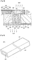
wavelength conversion member 400 includes anincident surface 401, anexit surface 404, a firstinclined surface 402 and a secondinclined surface 403. In detail, thetube 410 includes theincident surface 401, theexit surface 404, the firstinclined surface 402 and the secondinclined surface 403. - The
incident surface 401 of thewavelength conversion member 400 is opposite to thelight emitting diodes 300. That is, the incident,surface 401 of thewavelength conversion member 400 is directed toward thelight emitting diodes 300. Theincident surface 401 of thewavelength conversion member 400 is opposite to theexit surface 404 of thewavelength conversion member 400. Theincident surface 401 of thewavelength conversion member 400 may be substantially perpendicular to the optical axis OA. In addition, theincident surface 401 of thewavelength conversion member 400 is substantially parallel to the exit surface of thelight emitting diode 300. - The
exit surface 404 of thewavelength conversion member 400 is opposite to theincident surface 401 of thewavelength conversion member 400. In addition, theexit surface 404 of thewavelength conversion member 400 is opposite to the incident surface of thelight guide plate 200. Theexit surface 404 of thewavelength conversion member 400 is substantially parallel to the incident surface of thelight guide plate 200. - An area of the
exit surface 404 of thewavelength conversion member 400 may be larger than that of theincident surface 401 of thewavelength conversion member 400. - The first
inclined surface 402 extends from theincident surface 401 of thewavelength conversion member 400 to theexit surface 404 of thewavelength conversion member 400. The firstinclined surface 402 is inclined with respect to theincident surface 401 of thewavelength conversion member 400. In addition, the firstinclined surface 402 is inclined with respect to a virtual surface, which is perpendicular to the optical axis OA of thelight emitting diode 300. - An obtuse angle is formed between the first
inclined surface 402 and theincident surface 401 of thewavelength conversion member 400. In detail, the angle between the firstinclined surface 402 and theincident surface 401 of thewavelength conversion member 400 may be in the range of about 100° to about 130°. - The second
inclined surface 403 extends from theincident surface 401 of thewavelength conversion member 400 to theexit surface 404 of thewavelength conversion member 400. The secondinclined surface 403 is inclined with respect to theincident surface 401 of thewavelength conversion member 400. In addition, the secondinclined surface 403 is inclined with respect to a virtual surface, which is perpendicular to the optical axis OA of thelight emitting diode 300. - An obtuse angle is formed between the second
inclined surface 403 and theincident surface 401 of thewavelength conversion member 400. In detail, the angle between the secondinclined surface 403 and theincident surface 401 of thewavelength conversion member 400 may be in the range of about 100° to about 130°. - The distance between the first and second
inclined surfaces inclined surfaces light emitting diodes 300. That is, thewavelength conversion member 400 has the radial structure. Thus, thewavelength conversion member 400 can effectively dissipate the heat. - The
heat transfer part 700 is interposed between thelight emitting diode 300 and thewavelength conversion member 400. In more detail, theheat transfer part 700 is provided on the exit surface of thelight emitting diode 300. Further, theheat transfer part 700 is provided on theincident surface 401 of thewavelength conversion member 400. In more detail, theheat transfer part 700 may closely adhere to the exit surface 301 of thelight emitting diode 300. Further, theheat transfer part 700 may closely adhere to theincident surface 401, the firstinclined surface 402 and the secondinclined surface 403 of thewavelength conversion member 400. - The
heat transfer part 700 is interposed between thelight guide plate 200 and thewavelength conversion member 400. Theheat transfer part 700 may closely adhere to thelight guide plate 200 and thewavelength conversion member 400. In more detail, theheat transfer part 700 may closely adhere to theexit surface 404 of thewavelength conversion member 400. - Further, the
heat transfer part 700 covers the firstinclined surface 402 and the secondinclined surface 403 of thewavelength conversion member 400. That is, theheat transfer part 700 surrounds thewavelength conversion member 400. Theheat transfer part 700 may closely adhere to the firstinclined surface 402 and the secondinclined surface 403 of thewavelength conversion member 400. - The
heat transfer part 700 is connected to theheat dissipation part 800. Theheat transfer part 700 may be directly or indirectly connected to theheat dissipation part 800. - The
heat transfer part 700 has high thermal conductivity. Theheat transfer part 700 may have a thermal conductivity in the range of about 1.5×10⁻⁴cal/(sec·cm·°C) to about 20×10-4cal/(sec·cm·°C). Theheat transfer part 700 may have thermal conductivity higher than that of thetube 410. - The
heat transfer part 700 is transparent. A refractive index of theheat transfer part 700 may be an intermediate value between refractive indexes of thetube 410 and a filling material of thelight emitting diode 300. In more detail, the refractive index of the heat transfer part may be in the range of about 1.5 to about 1.6. - The
heat transfer part 700 may include a polymer having a high thermal conductivity and transmissivity. In more detail, the material constituting theheat transfer part 700 may include silicon resin, epoxy resin, phenolic resin, urethane resin, or urea resin. - The
heat dissipation part 800 is connected to theheat transfer part 700. Theheat dissipation part 800 may be directly or indirectly connected to theheat transfer part 700. Theheat dissipation part 800 dissipates heat transferred from theheat transfer part 700. - Referring to
FIGS. 1 ,5, and 6 , theheat dissipating part 800 includes a firstheat dissipating part 810 and a secondheat dissipating part 820. - The first
heat dissipating part 810 is provided at theFPCB 600. In more detail, the firstheat dissipating part 810 is provided inside theFPCB 600. The firstheat dissipating part 810 may be included in theFPCB 600. In other words, the firstheat dissipating part 810 may be a part of theFPCB 600. - The first
heat dissipating part 810 may be provided on thewavelength conversion member 400. In addition, the firstheat dissipating part 810 may extend in the extension direction of thewavelength conversion member 400. In addition, the firstheat dissipating part 810 is connected to theheat transfer part 700. In more detail, the firstheat dissipating part 810 may directly make contact with theheat transfer part 700. - The first
heat dissipating part 810 may include a material having high thermal conductivity. For example, the firstheat dissipating part 810 may include metal such as copper (Cu). - As shown in
FIG. 5 , the firstheat dissipating part 810 includes acontact part 811, a connection via 812, and aheat radiation pad 813. - The
contact part 811 directly or indirectly makes contact with theheat transfer part 700. The connection via 812 is connected to thecontact part 811 and theheat radiation pad 813. In other words, the connection via 812 connects thecontact part 811 with theheat radiation pad 813. - The
heat radiation pad 813 is connected to the connection via 812. Theheat radiation pad 813 may be exposed to the outside. Theheat radiation pad 813 dissipates heat transferred from theheat transfer part 700 to the outside, especially, into the atmosphere. - The second
heat dissipating part 820 is provided under thewavelength conversion member 400. In more detail, the secondheat dissipating part 820 may be provided under thelight emitting diodes 300. The secondheat dissipating part 820 is connected to theheat transfer part 700. In more detail, the secondheat dissipating part 820 may directly make contact with theheat transfer part 700. - The second
heat dissipating part 820 may have a shape extending in an extension direction of thewavelength conversion member 400. For example, the secondheat dissipating part 820 may have a bar shape or a strip shape extending in the extension direction of thewavelength conversion member 400. - The second
heat dissipating part 820 may include a material having high thermal conductivity. For example, the secondheat dissipating part 820 may include metal such as aluminum (Al) or copper (Cu). - The second
heat dissipating part 820 dissipates heat transferred from theheat transfer part 700 to the outside, especially, into the atmosphere. - The
optical sheets 500 are disposed on thelight guide plate 200 to improve the characteristic of the light passing through theoptical sheets 500. - The
FPCB 600 is electrically connected to thelight emitting diodes 300. TheFPCB 600 may mount thelight emitting diodes 300 thereon. TheFPCB 600 is installed in themold frame 10 and arranged on thelight guide plate 200. - Referring to
FIG. 5 , theFPCB 600 may include the firstheat dissipating part 810. TheFPCB 600 may include asupport layer 610, afirst interconnection layer 620, asecond interconnection layer 630, a firstprotective layer 640, and a secondprotective layer 650. - The
support layer 610 supports thefirst interconnection layer 620, thesecond interconnection layer 630, the firstprotective layer 640, and the secondprotective layer 650. Thesupport layer 610 includes an insulating layer. Thesupport layer 610 may be flexible. The material constituting thesupport layer 610 may include polymer such as polyimide-based resin. - The
first interconnection layer 620 is provided on thesupport layer 610. Thefirst interconnection layer 620 may directly make contact with the top surface of thesupport layer 610. Thefirst interconnection layer 620 may include Cu. - The
second interconnection layer 630 is provided under thesupport layer 610. Thesecond interconnection layer 630 may directly make contact with the bottom surface of thesupport layer 610. Thesecond interconnection layer 630 may include Cu. The first and second interconnection layers 620 and 630 may be connected to each other through a via formed through thesupport layer 610. - The
second interconnection layer 630 is connected to thelight emitting diodes 300. In more detail, thelight emitting diodes 300 may be electrically connected to thesecond interconnection layer 630 through a solder or a bump. - The first
protective layer 640 is provided on thefirst interconnection layer 620. The firstprotective layer 640 covers thefirst interconnection layer 620. The firstprotective layer 640 protects thefirst interconnection layer 620. The firstprotective layer 640 may include an insulator such as polymer. - The second
protective layer 650 is provided under thesecond interconnection layer 630. The secondprotective layer 650 covers thesecond interconnection layer 630. The secondprotective layer 650 protects thesecond interconnection layer 630. The secondprotective layer 650 may include an insulator such as polymer. - The first
heat dissipating part 810 may be included in theFPCB 600. In other words, theheat radiation pad 813 may be formed in the same layer with thefirst interconnection layer 620. In addition, the connection via 812 may be formed through thesupport layer 610. The connection via 812 may be formed in the same layer with thesecond interconnection layer 630. In addition, the firstprotective layer 640 may be formed therein with a first open region OR1 to expose the top surface of theheat radiation pad 813 to the outside. In addition, the secondprotective layer 650 may be formed therein with a second open region OR2 to expose thecontact part 811 to thewavelength conversion member 400. - The backlight unit is constructed by the
mold frame 10 and the backlight assembly 20. In other words, the backlight unit includes themold frame 10 and the backlight assembly 20. - The
liquid crystal panel 30 is provided inside themold frame 10, and arranged on theoptical sheets 500. - The
liquid crystal panel 30 displays images by adjusting intensity of the light passing through theliquid crystal panel 30. That is, theliquid crystal panel 30 is a display panel to display the images. Theliquid crystal panel 30 includes a TFT substrate, a color filter substrate, a liquid crystal layer interposed between the above two substrates and polarizing filters. - As described above, the liquid crystal display according to the embodiment may efficiently dissipate heat generated from the
light emitting diode 300 using theheat transfer part 700 and theheat dissipation part 800. Particularly, theheat transfer part 700 is interposed between thelight emitting diode 300 and thewavelength conversion member 400 and absorbs the heat dissipated from thelight emitting diode 300 toward thewavelength conversion member 400. - That is, the
heat transfer part 700 transfers the heat, which is dissipated from thelight emitting diode 300 to thewavelength conversion member 400, to theheat dissipation part 800. Further, the display device according to the embodiment dissipates heat generated from thewavelength conversion member 400 by light output from the light source using theheat transfer part 700 and theheat dissipation part 800. - In particular, since the
wavelength conversion member 400 includes the first and secondinclined surfaces wavelength conversion member 400 can be increased. Thus, the contact area between thewavelength conversion member 400 and theheat transfer part 700 can be enlarged. In addition, due to the inclination structure of the first and secondinclined surfaces heat transfer part 700 filled around the first and secondinclined surfaces 402 may be increased. - Thus, heat of the
wavelength conversion member 400 can be effectively transferred to theheat dissipation part 800 through theheat transfer part 700. - Accordingly, the display device according to the embodiment can prevent the
wavelength conversion member 400 from being degraded or denatured due to the heat. Particularly, the display device according to the embodiment may prevent ahost 440 and/or awavelength conversion particles 430 from being denatured caused by heat. Therefore, the liquid crystal display according to the embodiment can represent improved reliability and durability. - In addition, the display device according to the embodiment can efficiently reduce the temperature of the
wavelength conversion member 400. Therefore, the display device according to the embodiment can reduce the performance degradation of thewavelength conversion particles 430 caused by the temperature increase and can represent an improved color reproduction. -
FIG. 7 is a perspective view showing a wavelength conversion member according to an example not falling under the scope of the claims andFIG. 8 is a sectional view showing a light emitting diode, a flexible printed circuit board, a wavelength conversion member, and a light guide plate according to the example. Hereinafter, the wavelength conversion member according to this example will be described by making reference to the above description of the liquid crystal display. - Referring to
FIGS. 7 and8 , theincident surface 401 of thewavelength conversion member 400 is inclined with respect to a virtual surface, which is perpendicular to the optical axis OA of thelight emitting diode 300. In the same way, theexit surface 404 of thewavelength conversion member 400 is inclined with respect to the virtual surface, which is perpendicular to the optical axis OA of thelight emitting diode 300. - At this time, the
incident surface 401 and theexit surface 404 of thewavelength conversion member 400 may be substantially parallel to each other. - In addition, the
wavelength conversion member 400 may include atop surface 405 and abottom surface 406. Thetop surface 405 and thebottom surface 406 of thewavelength conversion member 400 may extend from theincident surface 401 to theexit surface 404 of thewavelength conversion member 400. In addition, thetop surface 405 and thebottom surface 406 of thewavelength conversion member 400 may face each other. Further, thetop surface 405 and thebottom surface 406 of thewavelength conversion member 400 are substantially parallel to the optical axis OA of thelight emitting diode 300. - That is, the
wavelength conversion member 400 may have the trapezoidal sectional shape. Thus, an acute angle is formed between thetop surface 405 and theincident surface 401 of thewavelength conversion member 400, and an obtuse angle is formed between thebottom surface 406 and theincident surface 401 of thewavelength conversion member 400. In addition, the distance D between theincident surface 401 of thewavelength conversion member 400 and the exit surface of thelight emitting diode 300 is gradually increased in the downward direction. That is, the upper portion of thewavelength conversion member 400 is closer to thelight emitting diode 300 in comparison with the lower portion of thewavelength conversion member 400. - Therefore, the thickness of the
heat transfer part 700 may be gradually increased as theheat transfer part 700 is located closely to the secondheat dissipation part 820. Thus, the liquid crystal display according to this example can effectively dissipate the heat of thewavelength conversion member 400 through the secondheat dissipation part 820. - In addition, since the outer surface area of the
wavelength conversion member 400 can be increased, the liquid crystal display according to this example can effectively dissipate the heat of thewavelength conversion member 400. -
FIG. 9 is a perspective view showing a wavelength conversion member according to a further example not falling under the scope of the claims andFIG. 10 is a sectional view showing a light emitting diode, a flexible printed circuit board, a wavelength conversion member, and a light guide plate according to this further example. Hereinafter, the wavelength conversion member according to this further example will be described by making reference to the above description of the liquid crystal display. - Referring to
FIGS. 9 and10 , theincident surface 401 of thewavelength conversion member 400 is inclined with respect to a virtual surface, which is perpendicular to the optical axis OA of thelight emitting diode 300. In the same way, theexit surface 404 of thewavelength conversion member 400 is inclined with respect to the virtual surface, which is perpendicular to the optical axis OA of thelight emitting diode 300. That is, theincident surface 401 and theexit surface 404 of thewavelength conversion member 400 are inclined surfaces inclined with respect to the virtual surface, which is perpendicular to the optical axis OA of thelight emitting diode 300. - At this time, the
incident surface 401 and theexit surface 404 of thewavelength conversion member 400 may be substantially parallel to each other. - In addition, the
wavelength conversion member 400 may include atop surface 405 and abottom surface 406. Thetop surface 405 and thebottom surface 406 of thewavelength conversion member 400 may extend from theincident surface 401 to theexit surface 404 of thewavelength conversion member 400. In addition, thetop surface 405 and thebottom surface 406 of thewavelength conversion member 400 may face each other. Further, thetop surface 405 and thebottom surface 406 of thewavelength conversion member 400 may be substantially parallel to the optical axis OA of thelight emitting diode 300. - That is, the
wavelength conversion member 400 may have the trapezoidal sectional shape. Thus, an obtuse angle is formed between thetop surface 405 and theincident surface 401 of thewavelength conversion member 400, and an acute angle is formed between thebottom surface 406 and theincident surface 401 of thewavelength conversion member 400. In addition, the distance D between theincident surface 401 of thewavelength conversion member 400 and the exit surface of thelight emitting diode 300 is gradually increased in the upward direction. That is, the lower portion of thewavelength conversion member 400 is closer to thelight emitting diode 300 in comparison with the upper portion of thewavelength conversion member 400. - Therefore, the thickness of the
heat transfer part 700 may be gradually increased as theheat transfer part 700 is located closely to the firstheat dissipation part 810. Thus, the liquid crystal display according to this example can effectively dissipate the heat of thewavelength conversion member 400 through the firstheat dissipation part 810. - In addition, since the outer surface area of the
wavelength conversion member 400 can be increased, the liquid crystal display according to this example can effectively dissipate the heat of thewavelength conversion member 400. - Although embodiments have been described with reference to a number of illustrative embodiments thereof, it should be understood that numerous other modifications and embodiments can be devised by those skilled in the art that will fall within the scope of the invention as defined by the appended claims.
Claims (10)
- A display device comprising:a plurality of LEDs (300) configured to emit light in the direction of an optical axis (OA);a wavelength conversion member (400) adjacent to the plurality of LEDs (300) for converting the wavelength of light emitted from the LEDS;a heat transfer part (700) between the plurality of LEDs (300) and the wavelength conversion member (400);a heat dissipation part (800) connected to the heat transfer part (700); anda display panel (30) to which light output from the wavelength conversion member (400) is incident,wherein the wavelength conversion member (400) comprises:an incident surface (401) opposite to the plurality of LEDs;an exit surface (404) opposite to the incident surface(401); anda first inclined surface (402) extending from the incident surface (401) to the exit surface (404), wherein the first inclined surface (402) is inclined with respect to the incident surface (401) of the wavelength conversion member and with respect to a surface which is perpendicular to the optical axis (OA),wherein the heat transfer part (700) is transparent andwherein the heat transfer part (700) is disposed on the incident surface (401) andon the exit surface (404) of the wavelength conversion member (400) covers the first inclined surface (402) of the wavelength conversion member (400),whereby the heat transfer part (700) is in contact with the wavelength conversion member (400), and further characterised in that the display device comprisesa reflective sheet (100);a light guide plate (200) on the reflective sheet (100), comprising an incident surface facing the plurality of LEDs;a plurality of optical sheets (500) on the light guide plate (200);and the wavelerth conversion member (400) is interposed between the LEDS (300) and the light guide plate (200), and in that the wavelength conversion member (400) comprises a second inclined surface (403),
wherein the second inclined surface (403) is inclined with respect to the incident surface (401) of the wavelength conversion member (400) and with respect to a surface which is perpendicular to the optical axis (OA), wherein the heat transfer part (700) also covers the second inclined surface (403). - The display device of claim 1, wherein the heat transfer part (700) includes a transparent resin.
- The display device of claim 1, wherein the heat transfer part (700) closely adheres to the inclined surface (402, 403).
- The display device of claim 1, wherein an obtuse angle is formed between the incident surface (401) and each of the first and second inclined surfaces (402, 403).
- The display device of claim 4, wherein an angle between the incident surface (401) and each of the first and second inclined surfaces (402, 403) is in the range between 100° and 130°.
- The display device of claim 1, wherein the incident surface (401) has an area smaller than an area of the exit surface(404).
- The display device of claim 1, wherein the heat transfer part (700) has a refractive index in the range between 1.5 and 1.6.
- The display device of claim 1, wherein the wavelength conversion member (400) includes a tube (410) sealing a plurality quantum dots dispersed within a matrix (440).
- The display device of claim 1, wherein the heat transfer part (700) surrounds the wavelength conversion member (400).
- The display device of claim 1, wherein the distance between the first and second inclined surfaces (402, 403) is increased as the first and second inclined surfaces (402, 403) extend away from the LEDs (300).
Priority Applications (1)
| Application Number | Priority Date | Filing Date | Title |
|---|---|---|---|
| EP17166911.2A EP3217216B1 (en) | 2011-07-18 | 2012-06-26 | Display device |
Applications Claiming Priority (2)
| Application Number | Priority Date | Filing Date | Title |
|---|---|---|---|
| KR1020110071140A KR101823684B1 (en) | 2011-07-18 | 2011-07-18 | Display device |
| PCT/KR2012/005052 WO2013012181A1 (en) | 2011-07-18 | 2012-06-26 | Display device |
Related Child Applications (2)
| Application Number | Title | Priority Date | Filing Date |
|---|---|---|---|
| EP17166911.2A Division EP3217216B1 (en) | 2011-07-18 | 2012-06-26 | Display device |
| EP17166911.2A Division-Into EP3217216B1 (en) | 2011-07-18 | 2012-06-26 | Display device |
Publications (3)
| Publication Number | Publication Date |
|---|---|
| EP2734893A1 EP2734893A1 (en) | 2014-05-28 |
| EP2734893A4 EP2734893A4 (en) | 2015-03-25 |
| EP2734893B1 true EP2734893B1 (en) | 2017-11-08 |
Family
ID=47558313
Family Applications (2)
| Application Number | Title | Priority Date | Filing Date |
|---|---|---|---|
| EP17166911.2A Active EP3217216B1 (en) | 2011-07-18 | 2012-06-26 | Display device |
| EP12815312.9A Active EP2734893B1 (en) | 2011-07-18 | 2012-06-26 | Display device |
Family Applications Before (1)
| Application Number | Title | Priority Date | Filing Date |
|---|---|---|---|
| EP17166911.2A Active EP3217216B1 (en) | 2011-07-18 | 2012-06-26 | Display device |
Country Status (5)
| Country | Link |
|---|---|
| US (1) | US9244308B2 (en) |
| EP (2) | EP3217216B1 (en) |
| KR (1) | KR101823684B1 (en) |
| TW (1) | TWI463200B (en) |
| WO (1) | WO2013012181A1 (en) |
Families Citing this family (17)
| Publication number | Priority date | Publication date | Assignee | Title |
|---|---|---|---|---|
| KR101210066B1 (en) | 2011-01-31 | 2012-12-07 | 엘지이노텍 주식회사 | Light conversion member and display device having the same |
| KR101305696B1 (en) * | 2011-07-14 | 2013-09-09 | 엘지이노텍 주식회사 | Display device and optical member |
| KR20130009020A (en) | 2011-07-14 | 2013-01-23 | 엘지이노텍 주식회사 | Optical member, display device having the same and method of fabricating the same |
| KR101241549B1 (en) | 2011-07-18 | 2013-03-11 | 엘지이노텍 주식회사 | Optical member, display device having the same and method of fabricating the same |
| KR101893494B1 (en) | 2011-07-18 | 2018-08-30 | 엘지이노텍 주식회사 | Optical member and display device having the same |
| KR101262520B1 (en) | 2011-07-18 | 2013-05-08 | 엘지이노텍 주식회사 | Display device and mrthod of fabricating the same |
| KR101251815B1 (en) | 2011-11-07 | 2013-04-09 | 엘지이노텍 주식회사 | Optical sheet and display device having the same |
| US9864121B2 (en) | 2011-11-22 | 2018-01-09 | Samsung Electronics Co., Ltd. | Stress-resistant component for use with quantum dots |
| JPWO2015156226A1 (en) | 2014-04-08 | 2017-04-13 | Nsマテリアルズ株式会社 | Quantum dot and manufacturing method thereof, and molded body, sheet member, wavelength conversion member, and light emitting device using the quantum dot |
| CN105987325B (en) * | 2015-03-02 | 2019-02-15 | 南京瀚宇彩欣科技有限责任公司 | Quantum pipe, backlight module and liquid crystal display device |
| CN105158970B (en) * | 2015-08-21 | 2019-01-04 | 深圳市华星光电技术有限公司 | A kind of backlight module and display panel |
| KR20170026936A (en) * | 2015-08-31 | 2017-03-09 | 삼성디스플레이 주식회사 | Light guide plate and display device having the same |
| CN107302672A (en) * | 2016-04-15 | 2017-10-27 | 深圳市华想世纪科技有限公司 | A kind of quantum dot and the LCD TV of YAG fluorescent powder blending |
| KR102622721B1 (en) * | 2016-12-05 | 2024-01-09 | 삼성전자주식회사 | Display apparatus |
| DE102017101729A1 (en) * | 2017-01-30 | 2018-08-02 | Osram Opto Semiconductors Gmbh | Radiation-emitting device |
| KR102433161B1 (en) * | 2017-08-18 | 2022-08-17 | 삼성디스플레이 주식회사 | Optical member and display including the same |
| CN107807473B (en) * | 2017-10-25 | 2020-12-25 | Tcl华星光电技术有限公司 | Light conversion material packaging structure, backlight module and display device |
Family Cites Families (18)
| Publication number | Priority date | Publication date | Assignee | Title |
|---|---|---|---|---|
| WO2005106978A1 (en) | 2004-04-28 | 2005-11-10 | Matsushita Electric Industrial Co., Ltd. | Light-emitting device and method for manufacturing same |
| JP2005353650A (en) * | 2004-06-08 | 2005-12-22 | Matsushita Electric Ind Co Ltd | Led optical source and liquid crystal display device |
| JP4401348B2 (en) * | 2004-12-28 | 2010-01-20 | シャープ株式会社 | LIGHT EMITTING DEVICE AND LIGHTING DEVICE AND DISPLAY DEVICE USING THE SAME |
| JP4469307B2 (en) | 2005-05-31 | 2010-05-26 | セイコーインスツル株式会社 | Display device |
| JP2007265716A (en) | 2006-03-28 | 2007-10-11 | Matsushita Electric Ind Co Ltd | Planar light source and liquid crystal display device |
| US7663152B2 (en) | 2006-08-09 | 2010-02-16 | Philips Lumileds Lighting Company, Llc | Illumination device including wavelength converting element side holding heat sink |
| JP2008251685A (en) * | 2007-03-29 | 2008-10-16 | Toshiba Corp | Light-emitting device and light generating module |
| JP2009038006A (en) | 2007-07-06 | 2009-02-19 | Citizen Electronics Co Ltd | Planar light-emitting device and display device |
| WO2009019836A2 (en) | 2007-08-03 | 2009-02-12 | Panasonic Corporation | Light-emitting device |
| DE102008012316B4 (en) * | 2007-09-28 | 2023-02-02 | OSRAM Opto Semiconductors Gesellschaft mit beschränkter Haftung | Semiconductor light source with a primary radiation source and a luminescence conversion element |
| JP5193586B2 (en) * | 2007-12-25 | 2013-05-08 | 株式会社東芝 | Semiconductor light emitting device |
| US8299701B2 (en) | 2007-12-27 | 2012-10-30 | Ge Lighting Solutions Llc | Lighting device having illumination, backlighting and display applications |
| KR101442146B1 (en) * | 2008-02-25 | 2014-09-23 | 삼성디스플레이 주식회사 | Light unit, liquid crystal display having the same and method of manufacturing the same |
| US20090237958A1 (en) * | 2008-03-21 | 2009-09-24 | Led Folio Corporation | Low-clearance light-emitting diode lighting |
| US7855394B2 (en) * | 2009-06-18 | 2010-12-21 | Bridgelux, Inc. | LED array package covered with a highly thermal conductive plate |
| KR20110012246A (en) | 2009-07-30 | 2011-02-09 | 엘지이노텍 주식회사 | Backlight unit |
| KR101508284B1 (en) * | 2009-12-15 | 2015-04-06 | 엘지이노텍 주식회사 | Back Light Unit Using Quantum Dots and Liquid Display Device Comprising of the Same |
| KR101241511B1 (en) * | 2011-03-22 | 2013-03-11 | 엘지이노텍 주식회사 | Light conversion member and display device having the same |
-
2011
- 2011-07-18 KR KR1020110071140A patent/KR101823684B1/en active IP Right Grant
-
2012
- 2012-06-26 EP EP17166911.2A patent/EP3217216B1/en active Active
- 2012-06-26 US US14/233,857 patent/US9244308B2/en active Active
- 2012-06-26 EP EP12815312.9A patent/EP2734893B1/en active Active
- 2012-06-26 WO PCT/KR2012/005052 patent/WO2013012181A1/en active Application Filing
- 2012-07-06 TW TW101124378A patent/TWI463200B/en active
Non-Patent Citations (1)
| Title |
|---|
| None * |
Also Published As
| Publication number | Publication date |
|---|---|
| KR20130010378A (en) | 2013-01-28 |
| KR101823684B1 (en) | 2018-01-30 |
| US20140168571A1 (en) | 2014-06-19 |
| EP2734893A4 (en) | 2015-03-25 |
| EP3217216A1 (en) | 2017-09-13 |
| WO2013012181A1 (en) | 2013-01-24 |
| TWI463200B (en) | 2014-12-01 |
| EP3217216B1 (en) | 2018-11-28 |
| TW201305631A (en) | 2013-02-01 |
| US9244308B2 (en) | 2016-01-26 |
| EP2734893A1 (en) | 2014-05-28 |
Similar Documents
| Publication | Publication Date | Title |
|---|---|---|
| EP2734893B1 (en) | Display device | |
| US9664843B2 (en) | Display device | |
| US9720160B2 (en) | Display device and optical member | |
| USRE47584E1 (en) | Display device | |
| US9110203B2 (en) | Display device with light guide plate and optical path conversion unit | |
| US9244209B2 (en) | Display device | |
| KR101210163B1 (en) | Optical sheet and method of fabricating the same | |
| US8562198B2 (en) | Optical member and display device | |
| EP2734875B1 (en) | Optical member and display device having the same | |
| KR101251807B1 (en) | Display device | |
| KR101792882B1 (en) | Optical member and method of fabricating the same | |
| KR101210084B1 (en) | Optical member and method of fabricating the same | |
| KR101854773B1 (en) | Optical member and display device having the same | |
| KR101251775B1 (en) | Optical member, display device having the same and method of fabricating the same | |
| KR101189326B1 (en) | Display and method of fabricating wavelength conversion member | |
| KR101846208B1 (en) | Display device | |
| KR101862864B1 (en) | Display device | |
| KR101294427B1 (en) | Display device and mrthod of fabricating the same | |
| KR101349426B1 (en) | Optical member and display device |
Legal Events
| Date | Code | Title | Description |
|---|---|---|---|
| PUAI | Public reference made under article 153(3) epc to a published international application that has entered the european phase |
Free format text: ORIGINAL CODE: 0009012 |
|
| 17P | Request for examination filed |
Effective date: 20140122 |
|
| AK | Designated contracting states |
Kind code of ref document: A1 Designated state(s): AL AT BE BG CH CY CZ DE DK EE ES FI FR GB GR HR HU IE IS IT LI LT LU LV MC MK MT NL NO PL PT RO RS SE SI SK SM TR |
|
| DAX | Request for extension of the european patent (deleted) | ||
| A4 | Supplementary search report drawn up and despatched |
Effective date: 20150225 |
|
| RIC1 | Information provided on ipc code assigned before grant |
Ipc: G02F 1/13357 20060101AFI20150219BHEP |
|
| 17Q | First examination report despatched |
Effective date: 20160808 |
|
| GRAP | Despatch of communication of intention to grant a patent |
Free format text: ORIGINAL CODE: EPIDOSNIGR1 |
|
| INTG | Intention to grant announced |
Effective date: 20170123 |
|
| GRAJ | Information related to disapproval of communication of intention to grant by the applicant or resumption of examination proceedings by the epo deleted |
Free format text: ORIGINAL CODE: EPIDOSDIGR1 |
|
| INTC | Intention to grant announced (deleted) | ||
| RAP1 | Party data changed (applicant data changed or rights of an application transferred) |
Owner name: LG INNOTEK CO., LTD. |
|
| GRAP | Despatch of communication of intention to grant a patent |
Free format text: ORIGINAL CODE: EPIDOSNIGR1 |
|
| INTG | Intention to grant announced |
Effective date: 20170529 |
|
| GRAS | Grant fee paid |
Free format text: ORIGINAL CODE: EPIDOSNIGR3 |
|
| GRAA | (expected) grant |
Free format text: ORIGINAL CODE: 0009210 |
|
| AK | Designated contracting states |
Kind code of ref document: B1 Designated state(s): AL AT BE BG CH CY CZ DE DK EE ES FI FR GB GR HR HU IE IS IT LI LT LU LV MC MK MT NL NO PL PT RO RS SE SI SK SM TR |
|
| REG | Reference to a national code |
Ref country code: GB Ref legal event code: FG4D |
|
| REG | Reference to a national code |
Ref country code: CH Ref legal event code: EP Ref country code: AT Ref legal event code: REF Ref document number: 944699 Country of ref document: AT Kind code of ref document: T Effective date: 20171115 |
|
| REG | Reference to a national code |
Ref country code: IE Ref legal event code: FG4D |
|
| REG | Reference to a national code |
Ref country code: DE Ref legal event code: R096 Ref document number: 602012039586 Country of ref document: DE |
|
| REG | Reference to a national code |
Ref country code: NL Ref legal event code: MP Effective date: 20171108 |
|
| REG | Reference to a national code |
Ref country code: LT Ref legal event code: MG4D |
|
| REG | Reference to a national code |
Ref country code: AT Ref legal event code: MK05 Ref document number: 944699 Country of ref document: AT Kind code of ref document: T Effective date: 20171108 |
|
| PG25 | Lapsed in a contracting state [announced via postgrant information from national office to epo] |
Ref country code: LT Free format text: LAPSE BECAUSE OF FAILURE TO SUBMIT A TRANSLATION OF THE DESCRIPTION OR TO PAY THE FEE WITHIN THE PRESCRIBED TIME-LIMIT Effective date: 20171108 Ref country code: FI Free format text: LAPSE BECAUSE OF FAILURE TO SUBMIT A TRANSLATION OF THE DESCRIPTION OR TO PAY THE FEE WITHIN THE PRESCRIBED TIME-LIMIT Effective date: 20171108 Ref country code: NL Free format text: LAPSE BECAUSE OF FAILURE TO SUBMIT A TRANSLATION OF THE DESCRIPTION OR TO PAY THE FEE WITHIN THE PRESCRIBED TIME-LIMIT Effective date: 20171108 Ref country code: NO Free format text: LAPSE BECAUSE OF FAILURE TO SUBMIT A TRANSLATION OF THE DESCRIPTION OR TO PAY THE FEE WITHIN THE PRESCRIBED TIME-LIMIT Effective date: 20180208 Ref country code: SE Free format text: LAPSE BECAUSE OF FAILURE TO SUBMIT A TRANSLATION OF THE DESCRIPTION OR TO PAY THE FEE WITHIN THE PRESCRIBED TIME-LIMIT Effective date: 20171108 Ref country code: ES Free format text: LAPSE BECAUSE OF FAILURE TO SUBMIT A TRANSLATION OF THE DESCRIPTION OR TO PAY THE FEE WITHIN THE PRESCRIBED TIME-LIMIT Effective date: 20171108 |
|
| REG | Reference to a national code |
Ref country code: FR Ref legal event code: PLFP Year of fee payment: 7 |
|
| PG25 | Lapsed in a contracting state [announced via postgrant information from national office to epo] |
Ref country code: HR Free format text: LAPSE BECAUSE OF FAILURE TO SUBMIT A TRANSLATION OF THE DESCRIPTION OR TO PAY THE FEE WITHIN THE PRESCRIBED TIME-LIMIT Effective date: 20171108 Ref country code: GR Free format text: LAPSE BECAUSE OF FAILURE TO SUBMIT A TRANSLATION OF THE DESCRIPTION OR TO PAY THE FEE WITHIN THE PRESCRIBED TIME-LIMIT Effective date: 20180209 Ref country code: AT Free format text: LAPSE BECAUSE OF FAILURE TO SUBMIT A TRANSLATION OF THE DESCRIPTION OR TO PAY THE FEE WITHIN THE PRESCRIBED TIME-LIMIT Effective date: 20171108 Ref country code: BG Free format text: LAPSE BECAUSE OF FAILURE TO SUBMIT A TRANSLATION OF THE DESCRIPTION OR TO PAY THE FEE WITHIN THE PRESCRIBED TIME-LIMIT Effective date: 20180208 Ref country code: IS Free format text: LAPSE BECAUSE OF FAILURE TO SUBMIT A TRANSLATION OF THE DESCRIPTION OR TO PAY THE FEE WITHIN THE PRESCRIBED TIME-LIMIT Effective date: 20180308 Ref country code: LV Free format text: LAPSE BECAUSE OF FAILURE TO SUBMIT A TRANSLATION OF THE DESCRIPTION OR TO PAY THE FEE WITHIN THE PRESCRIBED TIME-LIMIT Effective date: 20171108 Ref country code: RS Free format text: LAPSE BECAUSE OF FAILURE TO SUBMIT A TRANSLATION OF THE DESCRIPTION OR TO PAY THE FEE WITHIN THE PRESCRIBED TIME-LIMIT Effective date: 20171108 |
|
| PG25 | Lapsed in a contracting state [announced via postgrant information from national office to epo] |
Ref country code: SK Free format text: LAPSE BECAUSE OF FAILURE TO SUBMIT A TRANSLATION OF THE DESCRIPTION OR TO PAY THE FEE WITHIN THE PRESCRIBED TIME-LIMIT Effective date: 20171108 Ref country code: DK Free format text: LAPSE BECAUSE OF FAILURE TO SUBMIT A TRANSLATION OF THE DESCRIPTION OR TO PAY THE FEE WITHIN THE PRESCRIBED TIME-LIMIT Effective date: 20171108 Ref country code: EE Free format text: LAPSE BECAUSE OF FAILURE TO SUBMIT A TRANSLATION OF THE DESCRIPTION OR TO PAY THE FEE WITHIN THE PRESCRIBED TIME-LIMIT Effective date: 20171108 Ref country code: CY Free format text: LAPSE BECAUSE OF FAILURE TO SUBMIT A TRANSLATION OF THE DESCRIPTION OR TO PAY THE FEE WITHIN THE PRESCRIBED TIME-LIMIT Effective date: 20171108 Ref country code: CZ Free format text: LAPSE BECAUSE OF FAILURE TO SUBMIT A TRANSLATION OF THE DESCRIPTION OR TO PAY THE FEE WITHIN THE PRESCRIBED TIME-LIMIT Effective date: 20171108 |
|
| REG | Reference to a national code |
Ref country code: DE Ref legal event code: R097 Ref document number: 602012039586 Country of ref document: DE |
|
| PG25 | Lapsed in a contracting state [announced via postgrant information from national office to epo] |
Ref country code: IT Free format text: LAPSE BECAUSE OF FAILURE TO SUBMIT A TRANSLATION OF THE DESCRIPTION OR TO PAY THE FEE WITHIN THE PRESCRIBED TIME-LIMIT Effective date: 20171108 Ref country code: PL Free format text: LAPSE BECAUSE OF FAILURE TO SUBMIT A TRANSLATION OF THE DESCRIPTION OR TO PAY THE FEE WITHIN THE PRESCRIBED TIME-LIMIT Effective date: 20171108 Ref country code: SM Free format text: LAPSE BECAUSE OF FAILURE TO SUBMIT A TRANSLATION OF THE DESCRIPTION OR TO PAY THE FEE WITHIN THE PRESCRIBED TIME-LIMIT Effective date: 20171108 Ref country code: RO Free format text: LAPSE BECAUSE OF FAILURE TO SUBMIT A TRANSLATION OF THE DESCRIPTION OR TO PAY THE FEE WITHIN THE PRESCRIBED TIME-LIMIT Effective date: 20171108 |
|
| PLBE | No opposition filed within time limit |
Free format text: ORIGINAL CODE: 0009261 |
|
| STAA | Information on the status of an ep patent application or granted ep patent |
Free format text: STATUS: NO OPPOSITION FILED WITHIN TIME LIMIT |
|
| 26N | No opposition filed |
Effective date: 20180809 |
|
| PG25 | Lapsed in a contracting state [announced via postgrant information from national office to epo] |
Ref country code: SI Free format text: LAPSE BECAUSE OF FAILURE TO SUBMIT A TRANSLATION OF THE DESCRIPTION OR TO PAY THE FEE WITHIN THE PRESCRIBED TIME-LIMIT Effective date: 20171108 |
|
| REG | Reference to a national code |
Ref country code: CH Ref legal event code: PL |
|
| GBPC | Gb: european patent ceased through non-payment of renewal fee |
Effective date: 20180626 |
|
| REG | Reference to a national code |
Ref country code: BE Ref legal event code: MM Effective date: 20180630 |
|
| REG | Reference to a national code |
Ref country code: IE Ref legal event code: MM4A |
|
| PG25 | Lapsed in a contracting state [announced via postgrant information from national office to epo] |
Ref country code: LU Free format text: LAPSE BECAUSE OF NON-PAYMENT OF DUE FEES Effective date: 20180626 Ref country code: MC Free format text: LAPSE BECAUSE OF FAILURE TO SUBMIT A TRANSLATION OF THE DESCRIPTION OR TO PAY THE FEE WITHIN THE PRESCRIBED TIME-LIMIT Effective date: 20171108 |
|
| PG25 | Lapsed in a contracting state [announced via postgrant information from national office to epo] |
Ref country code: IE Free format text: LAPSE BECAUSE OF NON-PAYMENT OF DUE FEES Effective date: 20180626 Ref country code: CH Free format text: LAPSE BECAUSE OF NON-PAYMENT OF DUE FEES Effective date: 20180630 Ref country code: LI Free format text: LAPSE BECAUSE OF NON-PAYMENT OF DUE FEES Effective date: 20180630 Ref country code: GB Free format text: LAPSE BECAUSE OF NON-PAYMENT OF DUE FEES Effective date: 20180626 |
|
| PG25 | Lapsed in a contracting state [announced via postgrant information from national office to epo] |
Ref country code: BE Free format text: LAPSE BECAUSE OF NON-PAYMENT OF DUE FEES Effective date: 20180630 |
|
| PG25 | Lapsed in a contracting state [announced via postgrant information from national office to epo] |
Ref country code: MT Free format text: LAPSE BECAUSE OF NON-PAYMENT OF DUE FEES Effective date: 20180626 |
|
| PG25 | Lapsed in a contracting state [announced via postgrant information from national office to epo] |
Ref country code: TR Free format text: LAPSE BECAUSE OF FAILURE TO SUBMIT A TRANSLATION OF THE DESCRIPTION OR TO PAY THE FEE WITHIN THE PRESCRIBED TIME-LIMIT Effective date: 20171108 |
|
| PG25 | Lapsed in a contracting state [announced via postgrant information from national office to epo] |
Ref country code: HU Free format text: LAPSE BECAUSE OF FAILURE TO SUBMIT A TRANSLATION OF THE DESCRIPTION OR TO PAY THE FEE WITHIN THE PRESCRIBED TIME-LIMIT; INVALID AB INITIO Effective date: 20120626 Ref country code: PT Free format text: LAPSE BECAUSE OF FAILURE TO SUBMIT A TRANSLATION OF THE DESCRIPTION OR TO PAY THE FEE WITHIN THE PRESCRIBED TIME-LIMIT Effective date: 20171108 |
|
| PG25 | Lapsed in a contracting state [announced via postgrant information from national office to epo] |
Ref country code: MK Free format text: LAPSE BECAUSE OF NON-PAYMENT OF DUE FEES Effective date: 20171108 |
|
| PG25 | Lapsed in a contracting state [announced via postgrant information from national office to epo] |
Ref country code: AL Free format text: LAPSE BECAUSE OF FAILURE TO SUBMIT A TRANSLATION OF THE DESCRIPTION OR TO PAY THE FEE WITHIN THE PRESCRIBED TIME-LIMIT Effective date: 20171108 |
|
| PGFP | Annual fee paid to national office [announced via postgrant information from national office to epo] |
Ref country code: FR Payment date: 20230522 Year of fee payment: 12 Ref country code: DE Payment date: 20230522 Year of fee payment: 12 |