EP2733749A1 - A solar cell - Google Patents
A solar cell Download PDFInfo
- Publication number
- EP2733749A1 EP2733749A1 EP12193086.1A EP12193086A EP2733749A1 EP 2733749 A1 EP2733749 A1 EP 2733749A1 EP 12193086 A EP12193086 A EP 12193086A EP 2733749 A1 EP2733749 A1 EP 2733749A1
- Authority
- EP
- European Patent Office
- Prior art keywords
- solar cell
- layer
- cell according
- metal nanoparticles
- back contact
- Prior art date
- Legal status (The legal status is an assumption and is not a legal conclusion. Google has not performed a legal analysis and makes no representation as to the accuracy of the status listed.)
- Withdrawn
Links
- 239000004065 semiconductor Substances 0.000 claims abstract description 22
- 239000002082 metal nanoparticle Substances 0.000 claims abstract description 16
- 239000007769 metal material Substances 0.000 claims abstract description 13
- 239000002086 nanomaterial Substances 0.000 claims abstract description 11
- 239000011162 core material Substances 0.000 claims description 14
- 239000011257 shell material Substances 0.000 claims description 13
- 239000000463 material Substances 0.000 claims description 12
- BQCADISMDOOEFD-UHFFFAOYSA-N Silver Chemical compound [Ag] BQCADISMDOOEFD-UHFFFAOYSA-N 0.000 claims description 6
- 229910052709 silver Inorganic materials 0.000 claims description 6
- 239000004332 silver Substances 0.000 claims description 6
- PCHJSUWPFVWCPO-UHFFFAOYSA-N gold Chemical compound [Au] PCHJSUWPFVWCPO-UHFFFAOYSA-N 0.000 claims description 5
- 229910052737 gold Inorganic materials 0.000 claims description 5
- 239000010931 gold Substances 0.000 claims description 5
- RYGMFSIKBFXOCR-UHFFFAOYSA-N Copper Chemical compound [Cu] RYGMFSIKBFXOCR-UHFFFAOYSA-N 0.000 claims description 3
- 229910052802 copper Inorganic materials 0.000 claims description 3
- 239000010949 copper Substances 0.000 claims description 3
- 239000003989 dielectric material Substances 0.000 claims description 3
- 239000004411 aluminium Substances 0.000 claims description 2
- 229910052782 aluminium Inorganic materials 0.000 claims description 2
- XAGFODPZIPBFFR-UHFFFAOYSA-N aluminium Chemical compound [Al] XAGFODPZIPBFFR-UHFFFAOYSA-N 0.000 claims description 2
- 239000002105 nanoparticle Substances 0.000 description 17
- 239000006096 absorbing agent Substances 0.000 description 3
- 238000010521 absorption reaction Methods 0.000 description 3
- 230000000694 effects Effects 0.000 description 3
- 229910052751 metal Inorganic materials 0.000 description 3
- 239000002184 metal Substances 0.000 description 3
- 239000002245 particle Substances 0.000 description 3
- 239000010409 thin film Substances 0.000 description 3
- VYPSYNLAJGMNEJ-UHFFFAOYSA-N Silicium dioxide Chemical compound O=[Si]=O VYPSYNLAJGMNEJ-UHFFFAOYSA-N 0.000 description 2
- XUIMIQQOPSSXEZ-UHFFFAOYSA-N Silicon Chemical compound [Si] XUIMIQQOPSSXEZ-UHFFFAOYSA-N 0.000 description 2
- 230000003287 optical effect Effects 0.000 description 2
- 229910052710 silicon Inorganic materials 0.000 description 2
- 239000010703 silicon Substances 0.000 description 2
- GYHNNYVSQQEPJS-UHFFFAOYSA-N Gallium Chemical compound [Ga] GYHNNYVSQQEPJS-UHFFFAOYSA-N 0.000 description 1
- 239000004793 Polystyrene Substances 0.000 description 1
- 238000006243 chemical reaction Methods 0.000 description 1
- 239000011248 coating agent Substances 0.000 description 1
- 238000000576 coating method Methods 0.000 description 1
- 229910052733 gallium Inorganic materials 0.000 description 1
- 229910052738 indium Inorganic materials 0.000 description 1
- APFVFJFRJDLVQX-UHFFFAOYSA-N indium atom Chemical compound [In] APFVFJFRJDLVQX-UHFFFAOYSA-N 0.000 description 1
- 238000004519 manufacturing process Methods 0.000 description 1
- 229910000510 noble metal Inorganic materials 0.000 description 1
- 229920000642 polymer Polymers 0.000 description 1
- 229920002223 polystyrene Polymers 0.000 description 1
- 230000001902 propagating effect Effects 0.000 description 1
- 150000003346 selenoethers Chemical class 0.000 description 1
- 239000000377 silicon dioxide Substances 0.000 description 1
- 238000001228 spectrum Methods 0.000 description 1
- 239000000126 substance Substances 0.000 description 1
Images

Classifications
-
- H—ELECTRICITY
- H10—SEMICONDUCTOR DEVICES; ELECTRIC SOLID-STATE DEVICES NOT OTHERWISE PROVIDED FOR
- H10F—INORGANIC SEMICONDUCTOR DEVICES SENSITIVE TO INFRARED RADIATION, LIGHT, ELECTROMAGNETIC RADIATION OF SHORTER WAVELENGTH OR CORPUSCULAR RADIATION
- H10F77/00—Constructional details of devices covered by this subclass
- H10F77/20—Electrodes
- H10F77/244—Electrodes made of transparent conductive layers, e.g. transparent conductive oxide [TCO] layers
-
- H—ELECTRICITY
- H10—SEMICONDUCTOR DEVICES; ELECTRIC SOLID-STATE DEVICES NOT OTHERWISE PROVIDED FOR
- H10F—INORGANIC SEMICONDUCTOR DEVICES SENSITIVE TO INFRARED RADIATION, LIGHT, ELECTROMAGNETIC RADIATION OF SHORTER WAVELENGTH OR CORPUSCULAR RADIATION
- H10F10/00—Individual photovoltaic cells, e.g. solar cells
- H10F10/10—Individual photovoltaic cells, e.g. solar cells having potential barriers
- H10F10/16—Photovoltaic cells having only PN heterojunction potential barriers
- H10F10/167—Photovoltaic cells having only PN heterojunction potential barriers comprising Group I-III-VI materials, e.g. CdS/CuInSe2 [CIS] heterojunction photovoltaic cells
-
- H—ELECTRICITY
- H10—SEMICONDUCTOR DEVICES; ELECTRIC SOLID-STATE DEVICES NOT OTHERWISE PROVIDED FOR
- H10F—INORGANIC SEMICONDUCTOR DEVICES SENSITIVE TO INFRARED RADIATION, LIGHT, ELECTROMAGNETIC RADIATION OF SHORTER WAVELENGTH OR CORPUSCULAR RADIATION
- H10F77/00—Constructional details of devices covered by this subclass
- H10F77/10—Semiconductor bodies
- H10F77/12—Active materials
- H10F77/126—Active materials comprising only Group I-III-VI chalcopyrite materials, e.g. CuInSe2, CuGaSe2 or CuInGaSe2 [CIGS]
-
- Y—GENERAL TAGGING OF NEW TECHNOLOGICAL DEVELOPMENTS; GENERAL TAGGING OF CROSS-SECTIONAL TECHNOLOGIES SPANNING OVER SEVERAL SECTIONS OF THE IPC; TECHNICAL SUBJECTS COVERED BY FORMER USPC CROSS-REFERENCE ART COLLECTIONS [XRACs] AND DIGESTS
- Y02—TECHNOLOGIES OR APPLICATIONS FOR MITIGATION OR ADAPTATION AGAINST CLIMATE CHANGE
- Y02E—REDUCTION OF GREENHOUSE GAS [GHG] EMISSIONS, RELATED TO ENERGY GENERATION, TRANSMISSION OR DISTRIBUTION
- Y02E10/00—Energy generation through renewable energy sources
- Y02E10/50—Photovoltaic [PV] energy
- Y02E10/541—CuInSe2 material PV cells
Definitions
- the present invention relates to a solar cell, comprising a structure of sandwiched layers for converting incident light into electrical energy, the structure including an electrically conducting back contact layer, a light absorbing semiconductor layer located on the back contact layer, and a transparent conductive layer on top of the semiconductor layer, wherein the solar cell further comprises a group of metal nanoparticles forming a plasmonic nanostructure at a particular level in the sandwiched layers.
- Such solar cells are known, e.g. as thin-film silicon solar cells.
- the conventional solar cell layer structure containing a transparent conductive oxide (TCO) layer, a semiconductor layer and a back contact layer has been provided with a plasmonic nanostructure to increase the efficiency of the conversion from light to electric energy by scattering incident lightbeams.
- TCO transparent conductive oxide
- a semiconductor layer For thin-film silicon cells, efficiency enhancements of up to 44% have been demonstrated.
- these metal nanostructures can enable the use of thinner absorber layers without loss of efficiency. This is for example of interest for CIGS cells: these cells currently have a relatively thick, approx. 2.5 ⁇ m, and therefore expensive absorber layer. A significant reduction of absorber layer thickness without loss in efficiency would dramatically decrease the costs of a CIGS module.
- the metal nanomaterial are typically made from gold and silver.
- gold and silver material is costly.
- the metal nanoparticles have a core containing non-metallic material and a shell covering the core and containing metallic material.
- the invention is at least partly based on the surprising insight that the scattering effects of the nanoparticles depend on the metal material type, the particle size, the particle shape, the metal on the outer surface of the particle, the material type inside the nanoparticles, and the use of the nanoparticles in the layer structure of the solar cell, such as the distribution density, the material adjacent to the nanoparticles, the dimensions and other materials of the stack of layers etc. Also the ratio between scattering and absorption of the nanoparticles is determined by the above-mentioned parameters.
- metal nanoparticles having a core containing non-metallic material and a shell covering the core and containing metallic material generate comparable results in terms of scattering / absorption performance when comparing with massive nanoparticles, especially when using core material having a refractive index higher than 1, more preferably higher than circa 1.5. Then, costs can considerably be saved, since non-metallic core material is generally much cheaper than metallic material, at least when using noble metal material.
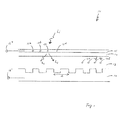
- FIG. 1 shows a schematic cross-sectional view of a solar cell 10 according to the invention.
- the solar cell 10 is of a so-called CIGS type, containing copper, indium, gallium and selenide in the light absorbing semiconductor material.
- the solar cell 10 includes a number of subsequent layers built upon each other forming a sandwich structure for converting incident light L i into electrical energy.
- the sandwich structure includes an electrically conducting back contact layer 12, a light absorbing semiconductor layer 13 located on the back contact layer 12, and a transparent conductive oxide (TCO) layer 15 on top of the semiconductor layer 13. Further, the sandwich structure includes a buffer layer 14 sandwiched between the TCO layer 15 and the semiconductor layer 13.
- the solar cell 10 also includes a pair of electrodes 16', 16" connected to the TOC layer 15 and to the back contact layer 12.
- the incident light L i is trapped in the semiconductor layer 13 accumulating an electric voltage on the electrodes 16', 16".
- the solar cell 10 further comprises a group of metal nanoparticles 17 forming a plasmonic nanostructure at a particular level in the sandwich structure.
- the plasmonic nanostructure 17 strongly interacts with the incident light L i generating scattered light beams L s for concentrating and folding light in the semiconductor layer 13.
- the plasmonic nanostructure 17 strongly interacts with the incident light L i generating scattered light beams L s for concentrating and folding light in the semiconductor layer 13.
- reflection to the TCO layer 15 is counteracted.
- the angular redistribution of the scattered light L s also contributes to light being trapped since the optical path length inside the semiconductor layer 134 is enlarged.
- the individual nanoparticles have a core 18 containing non-metallic material and a shell 19 covering the core and containing metallic material.
- FIG. 2 shows a schematic cross-sectional view of a metallic nanoparticle 17.
- the non-metallic core 18 material may e.g. include dielectric material and/or semiconductor material.
- the core 18 is made from a polymer dielectric such as polystyrene dielectric, or silica.
- the metallic shell material includes silver, gold, copper and/or aluminium.
- the shell 19 is made from silver since silver material is relatively stable, from a chemical point of view, and cheaper than gold.
- the shell 19 covers the core 18 as a coating or envelope.
- the nanoparticles 17 have a mainly spherical shape.
- the nanoparticles 17 can be made in other shapes as well, e.g. an ellipsoidal shape.
- the size of the metal nanoparticles 17 in at least one dimension ranges from circa 0.05 micrometer to circa 0.25 micrometer.
- the diameter d running through a center point 20 is preferably within a range from circa 0.05 micrometer to circa 0.25 micrometer.
- the nanoparticles 17 are monodisperse having the same size.
- the sizes of the nanoparticles 17 have a certain size distribution.
- the scattering effects of the nanoparticles 17 decrease while the absorption of the incident light by the nanoparticles 17 increases, thereby reducing the efficiency of the solar cell 10.
- the dimensions of the nanoparticles 17 are too large, the increase in scattering effect diminishes, also in view of the sizes of other structures in the solar cell 10. Then, the increase in metallic shell material that is required for forming the shell 19 has no additional contribution to the efficiency in trapping light.
- the thickness th of the shell 19 is at most circa 0.05 micrometer. Typically, the shell thickness th ranges between circa 0.01 micrometer and circa 0.02 micrometer.
- the metal nanoparticles 17 are located on top of the TCO layer 15 or on top of the back contact layer 12. However, the metal nanoparticles 17 can also be embedded in the semiconductor layer 13, 14, as shown in Fig. 1 , or can be located on top of the TCO layer 16.
- the back contact layer 12 is provided with a grating profile having a spatial periodicity d to guide light having a matching wavelength range, thereby increasing the optical path length and the corresponding trapping occurrence.
- the back contact layer 12 has another profile, e.g. a flat interface with the semiconductor layer 13, 14.
- the plasmonic nanostructure in the structure of sandwiched layers can not only be applied to CIGS solar cells, but also in other solar cells such as thin-film Si solar cells.
- top layer can be applied, the top layer being transparent and electrically conductive.
Landscapes
- Photovoltaic Devices (AREA)
Abstract
The invention relates to a solar cell. The solar cell comprises a structure of sandwiched layers for converting incident light into electrical energy. The structure includes an electrically conducting back contact layer, a light absorbing semiconductor layer located on the back contact layer, and a transparent conductive layer on top of the semiconductor layer. Further, the structure includes a group of metal nanoparticles forming a plasmonic nanostructure at a particular level in the sandwiched layers. The metal nanoparticles have a core containing non-metallic material and a shell containing metallic material covering the core.
Description
- The present invention relates to a solar cell, comprising a structure of sandwiched layers for converting incident light into electrical energy, the structure including an electrically conducting back contact layer, a light absorbing semiconductor layer located on the back contact layer, and a transparent conductive layer on top of the semiconductor layer, wherein the solar cell further comprises a group of metal nanoparticles forming a plasmonic nanostructure at a particular level in the sandwiched layers.
- Such solar cells are known, e.g. as thin-film silicon solar cells. Here, the conventional solar cell layer structure containing a transparent conductive oxide (TCO) layer, a semiconductor layer and a back contact layer has been provided with a plasmonic nanostructure to increase the efficiency of the conversion from light to electric energy by scattering incident lightbeams. For thin-film silicon cells, efficiency enhancements of up to 44% have been demonstrated. Alternatively, these metal nanostructures can enable the use of thinner absorber layers without loss of efficiency. This is for example of interest for CIGS cells: these cells currently have a relatively thick, approx. 2.5 µm, and therefore expensive absorber layer. A significant reduction of absorber layer thickness without loss in efficiency would dramatically decrease the costs of a CIGS module.
- To obtain the above-mentioned enhancement in cell efficiency, the metal nanomaterial are typically made from gold and silver. However, gold and silver material is costly.
- It is an object of the invention to reduce the above-mentioned drawbacks while maintaining or further exploiting the above-mentioned advantages. More particular, it is an object of the invention to provide a solar cell having improved efficiency or similar efficiency with reduced thickness of semiconductor layer, while manufacturing costs are relatively moderate. Thereto, according to an aspect of the invention, the metal nanoparticles have a core containing non-metallic material and a shell covering the core and containing metallic material.
- It is noted that the invention is at least partly based on the surprising insight that the scattering effects of the nanoparticles depend on the metal material type, the particle size, the particle shape, the metal on the outer surface of the particle, the material type inside the nanoparticles, and the use of the nanoparticles in the layer structure of the solar cell, such as the distribution density, the material adjacent to the nanoparticles, the dimensions and other materials of the stack of layers etc. Also the ratio between scattering and absorption of the nanoparticles is determined by the above-mentioned parameters.
- Surprisingly, it has been found that metal nanoparticles having a core containing non-metallic material and a shell covering the core and containing metallic material generate comparable results in terms of scattering / absorption performance when comparing with massive nanoparticles, especially when using core material having a refractive index higher than 1, more preferably higher than circa 1.5. Then, costs can considerably be saved, since non-metallic core material is generally much cheaper than metallic material, at least when using noble metal material.
- It also appears that when applying the metal nanoparticles according to the invention, not only the efficiency of incident light in the blue part of the spectrum increases, but also the efficiency of incident light having higher wavelengths, e.g. up to circa 600 nm, 800 nm, or even higher.
- Other advantageous embodiments according to the invention are described in the following claims.
- By way of example only, embodiments of the present invention will now be described with reference to the accompanying figures in which
-
Fig. 1 shows a schematic cross-sectional view of a solar cell according to the invention; and -
Fig. 2 shows a schematic cross-sectional view of a metallic nanoparticle included in the solar cell ofFig. 1 . - The figures are merely schematic views of preferred embodiments according to the invention. In the figures, the same reference numbers refer to equal or corresponding parts.
-
Figure 1 shows a schematic cross-sectional view of a solar cell 10 according to the invention. The solar cell 10 is of a so-called CIGS type, containing copper, indium, gallium and selenide in the light absorbing semiconductor material. - The solar cell 10 includes a number of subsequent layers built upon each other forming a sandwich structure for converting incident light Li into electrical energy. The sandwich structure includes an electrically conducting
back contact layer 12, a light absorbingsemiconductor layer 13 located on theback contact layer 12, and a transparent conductive oxide (TCO)layer 15 on top of thesemiconductor layer 13. Further, the sandwich structure includes abuffer layer 14 sandwiched between theTCO layer 15 and thesemiconductor layer 13. The solar cell 10 also includes a pair of electrodes 16', 16" connected to theTOC layer 15 and to theback contact layer 12. - During operation of the
solar cell 12 the incident light Li is trapped in thesemiconductor layer 13 accumulating an electric voltage on the electrodes 16', 16". - The solar cell 10 further comprises a group of
metal nanoparticles 17 forming a plasmonic nanostructure at a particular level in the sandwich structure. In the embodiment shown inFig. 1 , the plasmonic nanostructure 17a-d on the left-hand side in theTCO layer 15, while the plasmonic nanostructure 17e-h on the right-hand side is embedded in thesemiconductor layer 13. - The
plasmonic nanostructure 17 strongly interacts with the incident light Li generating scattered light beams Ls for concentrating and folding light in thesemiconductor layer 13. By propagating the scattered light beams Ls into high-index material, reflection to theTCO layer 15 is counteracted. Further, the angular redistribution of the scattered light Ls also contributes to light being trapped since the optical path length inside the semiconductor layer 134 is enlarged. - The individual nanoparticles have a core 18 containing non-metallic material and a
shell 19 covering the core and containing metallic material. -
Figure 2 shows a schematic cross-sectional view of ametallic nanoparticle 17. The non-metallic core 18 material may e.g. include dielectric material and/or semiconductor material. As an example of dielectric material, the core 18 is made from a polymer dielectric such as polystyrene dielectric, or silica. Preferably, the metallic shell material includes silver, gold, copper and/or aluminium. Highly preferable, theshell 19 is made from silver since silver material is relatively stable, from a chemical point of view, and cheaper than gold. Theshell 19 covers the core 18 as a coating or envelope. - The
nanoparticles 17 have a mainly spherical shape. However, thenanoparticles 17 can be made in other shapes as well, e.g. an ellipsoidal shape. Generally, the size of themetal nanoparticles 17 in at least one dimension ranges from circa 0.05 micrometer to circa 0.25 micrometer. In case of a mainly spherical shape, as shown inFig. 2 , the diameter d running through acenter point 20 is preferably within a range from circa 0.05 micrometer to circa 0.25 micrometer. In an advantageous manner, thenanoparticles 17 are monodisperse having the same size. Alternatively, the sizes of thenanoparticles 17 have a certain size distribution. If the dimensions of thenanoparticles 17 are too small, the scattering effects of thenanoparticles 17 decrease while the absorption of the incident light by thenanoparticles 17 increases, thereby reducing the efficiency of the solar cell 10. On the other hand, if the dimensions of thenanoparticles 17 are too large, the increase in scattering effect diminishes, also in view of the sizes of other structures in the solar cell 10. Then, the increase in metallic shell material that is required for forming theshell 19 has no additional contribution to the efficiency in trapping light. - The thickness th of the
shell 19 is at most circa 0.05 micrometer. Typically, the shell thickness th ranges between circa 0.01 micrometer and circa 0.02 micrometer. - In preferred embodiments, the
metal nanoparticles 17 are located on top of theTCO layer 15 or on top of theback contact layer 12. However, themetal nanoparticles 17 can also be embedded in thesemiconductor layer Fig. 1 , or can be located on top of the TCO layer 16. - The
back contact layer 12 is provided with a grating profile having a spatial periodicity d to guide light having a matching wavelength range, thereby increasing the optical path length and the corresponding trapping occurrence. Alternatively, theback contact layer 12 has another profile, e.g. a flat interface with thesemiconductor layer - The invention is not restricted to the embodiments described herein. It will be understood that many variants are possible.
- As an example, the plasmonic nanostructure in the structure of sandwiched layers can not only be applied to CIGS solar cells, but also in other solar cells such as thin-film Si solar cells.
- Further, it is noted that as an alternative to the TCO layer, another top layer can be applied, the top layer being transparent and electrically conductive.
- Other such variants will be apparent for the person skilled in the art and are considered to fall within the scope of the invention as defined in the following claims.
Claims (11)
- A solar cell, comprising a structure of sandwiched layers for converting incident light into electrical energy, the structure including an electrically conducting back contact layer, a light absorbing semiconductor layer located on the back contact layer, and a transparent conductive layer on top of the semiconductor layer, wherein the solar cell further comprises a group of metal nanoparticles forming a plasmonic nanostructure at a particular level in the sandwiched layers, and wherein the metal nanoparticles have a core containing non-metallic material and a shell covering the core and containing metallic material.
- A solar cell according to claim 1, wherein the non-metallic core material includes dielectric material and/or semiconductor material.
- A solar cell according to claim 1 or 2, wherein the metallic shell material includes silver, gold, copper and/or aluminium.
- A solar cell according to any of the preceding claims, wherein the size of the metal nanoparticles in at least one dimension ranges from circa 0.05 micrometer to circa 0.25 micrometer.
- A solar cell according to any of the preceding claims, wherein the thickness of the shell is at most circa 0.05 micrometer.
- A solar cell according to any of the preceding claims, wherein the metal nanoparticles are mainly spherical.
- A solar cell according to any of the preceding claims, wherein the metal nanoparticles are embedded in the transparent conductive layer or in the semiconductor layer.
- A solar cell according to any of the preceding claims, wherein the metal nanoparticles are located on top of the transparent conductive layer or on top of the back contact layer.
- A solar cell according to any of the preceding claims, further comprising a pair of electrodes connected to the transparent conducting layer and to the back contact layer, respectively.
- A solar cell according to any of the preceding claims, wherein the semiconductor material contains CIGS material.
- A solar cell according to any of the preceding claims, wherein the transparent conductive layer is a transparent conductive oxide layer.
Priority Applications (1)
| Application Number | Priority Date | Filing Date | Title |
|---|---|---|---|
| EP12193086.1A EP2733749A1 (en) | 2012-11-16 | 2012-11-16 | A solar cell |
Applications Claiming Priority (1)
| Application Number | Priority Date | Filing Date | Title |
|---|---|---|---|
| EP12193086.1A EP2733749A1 (en) | 2012-11-16 | 2012-11-16 | A solar cell |
Publications (1)
| Publication Number | Publication Date |
|---|---|
| EP2733749A1 true EP2733749A1 (en) | 2014-05-21 |
Family
ID=47257504
Family Applications (1)
| Application Number | Title | Priority Date | Filing Date |
|---|---|---|---|
| EP12193086.1A Withdrawn EP2733749A1 (en) | 2012-11-16 | 2012-11-16 | A solar cell |
Country Status (1)
| Country | Link |
|---|---|
| EP (1) | EP2733749A1 (en) |
Citations (3)
| Publication number | Priority date | Publication date | Assignee | Title |
|---|---|---|---|---|
| WO1999046351A1 (en) * | 1998-03-11 | 1999-09-16 | Wm. Marsh Rice University | Metal nanoshells |
| JP2010021189A (en) * | 2008-07-08 | 2010-01-28 | Omron Corp | Photoelectric device |
| US8216872B1 (en) * | 2011-02-21 | 2012-07-10 | National Applied Research Laboratories | Method of integrating light-trapping layer to thin-film solar cell |
-
2012
- 2012-11-16 EP EP12193086.1A patent/EP2733749A1/en not_active Withdrawn
Patent Citations (3)
| Publication number | Priority date | Publication date | Assignee | Title |
|---|---|---|---|---|
| WO1999046351A1 (en) * | 1998-03-11 | 1999-09-16 | Wm. Marsh Rice University | Metal nanoshells |
| JP2010021189A (en) * | 2008-07-08 | 2010-01-28 | Omron Corp | Photoelectric device |
| US8216872B1 (en) * | 2011-02-21 | 2012-07-10 | National Applied Research Laboratories | Method of integrating light-trapping layer to thin-film solar cell |
Non-Patent Citations (3)
| Title |
|---|
| GUILATT O ET AL: "Light absorption enhancement in thin silicon film by embedded metallic nanoshells", OPTICS LETTERS, OSA, OPTICAL SOCIETY OF AMERICA, WASHINGTON, DC, US, vol. 35, no. 8, 15 April 2010 (2010-04-15), pages 1139 - 1141, XP001553204, ISSN: 0146-9592, DOI: 10.1364/OL.35.001139 * |
| NARGES F. FAHIM ET AL: "Simultaneous broadband light trapping and fill factor enhancement in crystalline silicon solar cells induced by Ag nanoparticles and nanoshells", OPTICS EXPRESS, vol. 20, no. S5, 10 September 2012 (2012-09-10), pages A694, XP055062884, ISSN: 1094-4087, DOI: 10.1364/OE.20.00A694 * |
| YI-MING BAI ET AL: "Dipolar and Quadrupolar Modes of SiO 2 /Au Nanoshell Enhanced Light Trapping in Thin Film Solar Cells", CHINESE PHYSICS LETTERS, vol. 28, no. 8, 1 August 2011 (2011-08-01), pages 087306, XP055063251, ISSN: 0256-307X, DOI: 10.1088/0256-307X/28/8/087306 * |
Similar Documents
| Publication | Publication Date | Title |
|---|---|---|
| Akimov et al. | Resonant and nonresonant plasmonic nanoparticle enhancement for thin-film silicon solar cells | |
| Deceglie et al. | Design of nanostructured solar cells using coupled optical and electrical modeling | |
| Pillai et al. | Plasmonics for photovoltaic applications | |
| Goffard et al. | Light trapping in ultrathin CIGS solar cells with nanostructured back mirrors | |
| Atwater et al. | Plasmonics for improved photovoltaic devices | |
| EP1650814B1 (en) | Tandem thin film solar cell | |
| Ghobadi et al. | Semiconductor thin film based metasurfaces and metamaterials for photovoltaic and photoelectrochemical water splitting applications | |
| Villesen et al. | Aluminum nanoparticles for plasmon-improved coupling of light into silicon | |
| US20130081693A1 (en) | Surface plasmon energy conversion device | |
| US20110186119A1 (en) | Light-trapping plasmonic back reflector design for solar cells | |
| JP7498368B2 (en) | Tandem photovoltaic device | |
| US20200028005A1 (en) | Bifacial Solar Modules Incorporating Effectively Transparent Contacts | |
| Yang et al. | Optimal design of ultra‐broadband, omnidirectional, and polarization‐insensitive amorphous silicon solar cells with a core‐shell nanograting structure | |
| Schmid et al. | Nanoparticles for light management in ultrathin chalcopyrite solar cells | |
| Yang et al. | Can plasmonic Al nanoparticles improve absorption in triple junction solar cells? | |
| Zand et al. | Design of GaAs-thin film solar cell using TiO2 hemispherical nanoparticles array | |
| Theuring et al. | Comparison of Ag and SiO2 nanoparticles for light trapping applications in silicon thin film solar cells | |
| US20140109965A1 (en) | Photoelectric conversion element | |
| Nguyen et al. | Plasmonic enhancement of light trapping into organic solar cells | |
| Poursafar et al. | Ultrathin tandem-plasmonic photovoltaic structures for synergistically enhanced light absorption | |
| CN110875399B (en) | Wide-spectrum absorption thin-film solar cell and photovoltaic power generation device | |
| TWI594450B (en) | Thin film solar cell light integration method and its structure | |
| Huang et al. | Plasmonic thin film solar cells | |
| Ye et al. | Embedded metal nanopatterns for near‐field scattering‐enhanced optical absorption | |
| Sun et al. | Surface plasmon enhanced light trapping in metal/silicon nanobowl arrays for thin film photovoltaics |
Legal Events
| Date | Code | Title | Description |
|---|---|---|---|
| PUAI | Public reference made under article 153(3) epc to a published international application that has entered the european phase |
Free format text: ORIGINAL CODE: 0009012 |
|
| 17P | Request for examination filed |
Effective date: 20121116 |
|
| AK | Designated contracting states |
Kind code of ref document: A1 Designated state(s): AL AT BE BG CH CY CZ DE DK EE ES FI FR GB GR HR HU IE IS IT LI LT LU LV MC MK MT NL NO PL PT RO RS SE SI SK SM TR |
|
| AX | Request for extension of the european patent |
Extension state: BA ME |
|
| STAA | Information on the status of an ep patent application or granted ep patent |
Free format text: STATUS: THE APPLICATION IS DEEMED TO BE WITHDRAWN |
|
| 18D | Application deemed to be withdrawn |
Effective date: 20141122 |