EP2733742A1 - Amplifier circuit - Google Patents
Amplifier circuit Download PDFInfo
- Publication number
- EP2733742A1 EP2733742A1 EP20120192808 EP12192808A EP2733742A1 EP 2733742 A1 EP2733742 A1 EP 2733742A1 EP 20120192808 EP20120192808 EP 20120192808 EP 12192808 A EP12192808 A EP 12192808A EP 2733742 A1 EP2733742 A1 EP 2733742A1
- Authority
- EP
- European Patent Office
- Prior art keywords
- support structure
- circuit
- connection elements
- void
- power amplifier
- Prior art date
- Legal status (The legal status is an assumption and is not a legal conclusion. Google has not performed a legal analysis and makes no representation as to the accuracy of the status listed.)
- Granted
Links
Images



Classifications
-
- H—ELECTRICITY
- H03—ELECTRONIC CIRCUITRY
- H03F—AMPLIFIERS
- H03F3/00—Amplifiers with only discharge tubes or only semiconductor devices as amplifying elements
- H03F3/68—Combinations of amplifiers, e.g. multi-channel amplifiers for stereophonics
-
- H—ELECTRICITY
- H03—ELECTRONIC CIRCUITRY
- H03F—AMPLIFIERS
- H03F1/00—Details of amplifiers with only discharge tubes, only semiconductor devices or only unspecified devices as amplifying elements
- H03F1/02—Modifications of amplifiers to raise the efficiency, e.g. gliding Class A stages, use of an auxiliary oscillation
- H03F1/0205—Modifications of amplifiers to raise the efficiency, e.g. gliding Class A stages, use of an auxiliary oscillation in transistor amplifiers
- H03F1/0288—Modifications of amplifiers to raise the efficiency, e.g. gliding Class A stages, use of an auxiliary oscillation in transistor amplifiers using a main and one or several auxiliary peaking amplifiers whereby the load is connected to the main amplifier using an impedance inverter, e.g. Doherty amplifiers
-
- H—ELECTRICITY
- H10—SEMICONDUCTOR DEVICES; ELECTRIC SOLID-STATE DEVICES NOT OTHERWISE PROVIDED FOR
- H10W—GENERIC PACKAGES, INTERCONNECTIONS, CONNECTORS OR OTHER CONSTRUCTIONAL DETAILS OF DEVICES COVERED BY CLASS H10
- H10W44/00—Electrical arrangements for controlling or matching impedance
- H10W44/20—Electrical arrangements for controlling or matching impedance at high-frequency [HF] or radio frequency [RF]
-
- H—ELECTRICITY
- H10—SEMICONDUCTOR DEVICES; ELECTRIC SOLID-STATE DEVICES NOT OTHERWISE PROVIDED FOR
- H10W—GENERIC PACKAGES, INTERCONNECTIONS, CONNECTORS OR OTHER CONSTRUCTIONAL DETAILS OF DEVICES COVERED BY CLASS H10
- H10W95/00—Packaging processes not covered by the other groups of this subclass
-
- H—ELECTRICITY
- H10—SEMICONDUCTOR DEVICES; ELECTRIC SOLID-STATE DEVICES NOT OTHERWISE PROVIDED FOR
- H10W—GENERIC PACKAGES, INTERCONNECTIONS, CONNECTORS OR OTHER CONSTRUCTIONAL DETAILS OF DEVICES COVERED BY CLASS H10
- H10W44/00—Electrical arrangements for controlling or matching impedance
- H10W44/20—Electrical arrangements for controlling or matching impedance at high-frequency [HF] or radio frequency [RF]
- H10W44/241—Electrical arrangements for controlling or matching impedance at high-frequency [HF] or radio frequency [RF] for passive devices or passive elements
- H10W44/243—Electrical arrangements for controlling or matching impedance at high-frequency [HF] or radio frequency [RF] for passive devices or passive elements for decoupling, e.g. bypass capacitors
-
- H—ELECTRICITY
- H10—SEMICONDUCTOR DEVICES; ELECTRIC SOLID-STATE DEVICES NOT OTHERWISE PROVIDED FOR
- H10W—GENERIC PACKAGES, INTERCONNECTIONS, CONNECTORS OR OTHER CONSTRUCTIONAL DETAILS OF DEVICES COVERED BY CLASS H10
- H10W72/00—Interconnections or connectors in packages
- H10W72/50—Bond wires
- H10W72/541—Dispositions of bond wires
- H10W72/5445—Dispositions of bond wires being orthogonal to a side surface of the chip, e.g. parallel arrangements
-
- H—ELECTRICITY
- H10—SEMICONDUCTOR DEVICES; ELECTRIC SOLID-STATE DEVICES NOT OTHERWISE PROVIDED FOR
- H10W—GENERIC PACKAGES, INTERCONNECTIONS, CONNECTORS OR OTHER CONSTRUCTIONAL DETAILS OF DEVICES COVERED BY CLASS H10
- H10W72/00—Interconnections or connectors in packages
- H10W72/50—Bond wires
- H10W72/541—Dispositions of bond wires
- H10W72/547—Dispositions of multiple bond wires
- H10W72/5473—Dispositions of multiple bond wires multiple bond wires connected to a common bond pad
-
- H—ELECTRICITY
- H10—SEMICONDUCTOR DEVICES; ELECTRIC SOLID-STATE DEVICES NOT OTHERWISE PROVIDED FOR
- H10W—GENERIC PACKAGES, INTERCONNECTIONS, CONNECTORS OR OTHER CONSTRUCTIONAL DETAILS OF DEVICES COVERED BY CLASS H10
- H10W72/00—Interconnections or connectors in packages
- H10W72/50—Bond wires
- H10W72/541—Dispositions of bond wires
- H10W72/547—Dispositions of multiple bond wires
- H10W72/5475—Dispositions of multiple bond wires multiple bond wires connected to common bond pads at both ends of the wires
-
- H—ELECTRICITY
- H10—SEMICONDUCTOR DEVICES; ELECTRIC SOLID-STATE DEVICES NOT OTHERWISE PROVIDED FOR
- H10W—GENERIC PACKAGES, INTERCONNECTIONS, CONNECTORS OR OTHER CONSTRUCTIONAL DETAILS OF DEVICES COVERED BY CLASS H10
- H10W90/00—Package configurations
- H10W90/701—Package configurations characterised by the relative positions of pads or connectors relative to package parts
- H10W90/751—Package configurations characterised by the relative positions of pads or connectors relative to package parts of bond wires
- H10W90/756—Package configurations characterised by the relative positions of pads or connectors relative to package parts of bond wires between a chip and a stacked lead frame, conducting package substrate or heat sink
Definitions
- This invention relates to an amplifier circuit, and more particularly to a packaged power amplifier circuit.
- Doherty Power Amplifier DPA
- RF Radio Frequency
- Doherty amplification is a well-known technique for improving the power efficiency of RF transmitters when dealing with modulated signals that have high peak-to-average ratios e.g. MC-GSM, WCDMA and OFDM (where power efficiency is defined as the ratio of average output power of the PA to the DC input power).
- Doherty amplification typically improves the average efficiency of a transmitter it is employed with and can provide average efficiencies of more than 50% for modern WCDMA and MC-GSM signals. It is therefore widely used in cellular and broadcast base-station transmitters.
- OMP MMIC dual-in-package
- Embodiments may reduce the electromagnetic coupling between two adjacent or neighbouring amplifiers fabricated on a die by having one or more voids formed in the supporting structure of the die. These voids may provide a "shortcut" for RF current returning to the die, and may be formed in both new and existing support structures.
- Embodiments employ the principle that at a RF frequency, currents follow a path of reduced inductance and so take a shorter path that may be defined by a void or hole in the support structure. Reduced inductance of a shorter return path may thus reduce cross-talk. Also, a shorter return path may reduce the amount of electromagnetic coupling between returning paths.
- an integrated power amplifier circuit according to independent claim 1.
- the at least one void may comprise: a first aperture formed in the support structure underneath a first set of one or more connection elements; and a second aperture formed in the support structure underneath a second set of one or more connection elements. In this way, a shorter return path may be provided for each set of one or more connection elements.
- connection elements may be wire bonds or bond re-bond connections.
- the at least one void may comprise a segment of the support structure that has been removed, the segment extending from an edge of the support structure towards the die.
- a void may be formed by removing a portion of an edge of the support structure. This enables simple formation of the void.
- a void may be formed by etching or drilling the supporting structure.
- the horizontal extent of the at least one aperture in a first direction may greater than that of the set of one or more bond wires which the at least one aperture is positioned underneath. This may help to ensure that all return current from the set of one or more bond wires is presented with a shorter return path.
- the integrated power amplifier circuit may be a Doherty power amplifier circuit, wherein the first amplifier is the main amplifier of the Doherty power amplifier circuit and the second amplifier is the peak amplifier of the Doherty power amplifier circuit.
- embodiments may provide a Doherty power amplifier circuit having reduced cross-talk between the main and peak amplifiers.
- Existing amplifier circuits may be modified according to an embodiment of the invention so as to reduce electromagnetic coupling between two adjacent or neighbouring amplifiers fabricated on a die.
- Embodiments may be employed in a radio frequency transmitter/receiver or a mobile communication base station.
- Embodiments may be packaged to provide a discrete integrated power amplifier circuit.
- Embodiments may be used in combination with other measures to further reduce cross-talk and achieve required specifications.
- FIG. 2 and3 there is shown a top and cross-sectional view, respectively, of an amplifier part of an integrated circuit according to an embodiment of the invention.
- the embodiment is a single-die, single-package dual amplifier product in over-mould-plastic (OMP).
- OMP over-mould-plastic
- the power amplifier circuit comprises first A1 and second A2 amplifiers fabricated on a single die 12 substantially adjacent to each other.
- the die 12 is mounted on a support structure14 having a flange 14F.
- the first A1 amplifier is former from first T1 and second T2 transistors
- the second amplifier A2 is formed from third T3 and fourth T4 transistors.
- First 16 to fourth 22 sets of bond wires are connected to the first to fourth transistors, respectively, at one end.
- the other ends of the sets of bond wires are connected to leads 24 which make an electrical connection with a printed circuit board (PCB) 26.
- PCB printed circuit board
- the sets of bond wires 16,18,20,22 are adapted to electrically connect the first A1 and second A2 amplifiers to appropriate parts of the PCB 26, such that the amplifiers A1 and A2 have their own input and output leads.
- the die 12 the first A1 and second A2 amplifiers, and the set of bond wires 16,18,20,22, and part of the leads 24 are all encased/covered in OMP 28.
- Matching Li wires and matching capacitors Ci are provided for each of the first T1 to fourth T4 transistors.
- the flange 14F of the support structure 14 comprises first 30 1 to fourth 30 4 apertures situated (at least in part) directly underneath the first 16 to fourth 22 sets of bond wires, respectively.
- each set of bond wires there is provided a portion of a hole/aperture 30 in the flange 14F of the support structure.
- the horizontal extent of each aperture a lateral direction i.e. the direction from top to bottom of the page of Figure 2 ), as indicated by the arrow labelled "W"
- W the horizontal extent of each aperture a lateral direction
- W is greater than the lateral extent of the set bond wires which the aperture is positioned below, as indicated by the arrow labelled "B".
- FIG 3 there is shown a cross-sectional view of the embodiment of Figure 2 taken along the line X-X (and in the direction indicated by the accompanying arrows).
- FIG 3 it is shown how, at a RF frequency, the return current takes the path of minimal inductance, and therefore of minimum distance.
- the aperture 30 3 provides a 'short-cut' for current return path as indicated by the solid black arrows labelled "P".
- the current return path would extend around the outside surface of the flange 14F as indicted by the dotted arrows labelled "Q".
- the aperture 30 3 provides a current return path of reduced length when compared to a conventional arrangement. This shorter return path provides a reduced inductance and thus helps to reduce cross-talk (e.g. by reducing parasitic coupling between the first A1 and second A2 amplifiers).
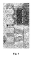
- Figure 4 shows the results of a 3D electromagnetic simulation for the embodiment of Figures 2 and 3 .
- the darker areas identify electromagnetic fields of greater magnitude than the lightly coloured areas.
- the electromagnetic field is concentrated within the vicinity of the first 16 and second 18 set of bond wires and does not spread to the third set of bond wires 20. This indicates that, with holes the apertures formed in the flange, the returning current of the first amplifier A1 is confined to its section and the electromagnetic coupling to the second amplifier A2 is significantly reduced.
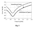
- FIG. 5 A benefit provided by the embodiment of Figures 2 and 3 is illustrated by the graph of Figure 5 , which plots the amount of cross-talk against frequency for a conventional integrated dual amplifier circuit and for the dual amplifier circuit of Figures 2 and 3 .
- the embodiment of the invention provide a reduction in cross-talk of approximately 5dB across a wide range of frequencies.
- the conventional circuit exhibits cross-talk of approximately -15dB at 2.14GHz (which is a commonly employed radio frequency)
- the embodiment of the invention exhibits cross-talk of approximately -21dB at 2.14GHz. This represents a significant decrease in cross-talk.
- FIG. 6 there is shown a modification to the embodiment of Figure 2 . Except for the apertures formed in the flange 14F of the support structure 14, the embodiment of Figure 6 does not differ from the embodiment of Figure 2 . A detailed description of all of the features shown in Figure 6 will therefore be omitted. However, where the embodiment of Figure 6 does differ is that first 30' 1 to fourth 30' 4 voids are formed in the flange 14F (instead of apertures like that in the embodiment of Figure 2 ). Here, the voids are oblong-shaped areas or segments that have been removed from the flange 14F.
- voids extend from the edge of the flange inwardly towards to the die to an extent that a portion of each void 30' 1 , 30' 2 , 30' 3 , 30' 4 is situated underneath a respective set of wire bonds 16,18,22,24.
- a void may comprise a segment of the support structure that has been removed.
- a void may be formed by removing a portion the support structure. This enables simple formation of the void (by chemical etching or mechanical drilling, for example).
- the above described embodiments comprise an amplifier formed from two transistors, other embodiments may employ amplifiers formed from one or more transistors, and the different amplifiers may be formed from different numbers of transistors.
- the above described embodiments comprise amplifier formed on a single die, other embodiment may comprise more than one die.
- the above described embodiment comprise a single aperture or void under each set of connection elements, alternative embodiments may employ other arrangements of apertures or void in the flange under the sets of connection elements.
- Figures 2 and 3 may be modified so as to comprise first and second voids in the flange, wherein the first void is situated underneath both the first and second sets of connection elements, and wherein the second void is situated underneath both the third and fourth sets of connection elements.
Landscapes
- Engineering & Computer Science (AREA)
- Power Engineering (AREA)
- Amplifiers (AREA)
Abstract
Description
- This invention relates to an amplifier circuit, and more particularly to a packaged power amplifier circuit.
- Power amplifier circuits, such as Doherty Power Amplifier (DPA) circuits are widely used in Radio Frequency (RF) power transmitters. Doherty amplification is a well-known technique for improving the power efficiency of RF transmitters when dealing with modulated signals that have high peak-to-average ratios e.g. MC-GSM, WCDMA and OFDM (where power efficiency is defined as the ratio of average output power of the PA to the DC input power).
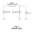
- A schematic of a DPA in its most elementary form is shown in
Figure 1 and details of its operation are well known in the field of amplifier circuits. Consequently, detailed explanation of the DPA ofFigure 1 will be omitted. - The concept of Doherty amplification typically improves the average efficiency of a transmitter it is employed with and can provide average efficiencies of more than 50% for modern WCDMA and MC-GSM signals. It is therefore widely used in cellular and broadcast base-station transmitters.
- It is widely known to combine the Main and Peak amplifier of a Doherty amplifier within a single package. In such packaged arrangements, crosstalk between the Main and Peak amplifier should be minimized in order to achieve optimal operation. It is known that to minimize crosstalk between the Main and Peak amplifiers, parasitic coupling should be avoided. This directly contradicts having two amplifiers placed next to each other in a single package because the close proximity of the amplifiers results into electromagnetic coupling at the input and output of the amplifying transistors.
- Measurements have shown that a typical isolation between two amplifiers in a dual-in-package (OMP MMIC) configuration is in the order of 15dB. This value is not considered acceptable for many applications.
- Proposed is a concept for reducing the amount of electromagnetic coupling between two adjacent amplifiers on a die of an integrated circuit. Embodiments may reduce the electromagnetic coupling between two adjacent or neighbouring amplifiers fabricated on a die by having one or more voids formed in the supporting structure of the die. These voids may provide a "shortcut" for RF current returning to the die, and may be formed in both new and existing support structures.
- Embodiments employ the principle that at a RF frequency, currents follow a path of reduced inductance and so take a shorter path that may be defined by a void or hole in the support structure. Reduced inductance of a shorter return path may thus reduce cross-talk. Also, a shorter return path may reduce the amount of electromagnetic coupling between returning paths.
- According to an aspect of the invention, there is provided an integrated power amplifier circuit according to independent claim 1.
- The at least one void may comprise: a first aperture formed in the support structure underneath a first set of one or more connection elements; and a second aperture formed in the support structure underneath a second set of one or more connection elements. In this way, a shorter return path may be provided for each set of one or more connection elements.
- The connection elements may be wire bonds or bond re-bond connections.
- The at least one void may comprise a segment of the support structure that has been removed, the segment extending from an edge of the support structure towards the die. In other words, a void may be formed by removing a portion of an edge of the support structure. This enables simple formation of the void. By way of example, a void may be formed by etching or drilling the supporting structure.
- The horizontal extent of the at least one aperture in a first direction may greater than that of the set of one or more bond wires which the at least one aperture is positioned underneath. This may help to ensure that all return current from the set of one or more bond wires is presented with a shorter return path.
- The integrated power amplifier circuit may be a Doherty power amplifier circuit, wherein the first amplifier is the main amplifier of the Doherty power amplifier circuit and the second amplifier is the peak amplifier of the Doherty power amplifier circuit. Thus, embodiments may provide a Doherty power amplifier circuit having reduced cross-talk between the main and peak amplifiers.
- Existing amplifier circuits may be modified according to an embodiment of the invention so as to reduce electromagnetic coupling between two adjacent or neighbouring amplifiers fabricated on a die.
- According to another aspect of the invention, there is provided a method of manufacturing an integrated power amplifier circuit according to
independent claim 12. - Embodiments may be employed in a radio frequency transmitter/receiver or a mobile communication base station.
- Embodiments may be packaged to provide a discrete integrated power amplifier circuit.
- Embodiments may be used in combination with other measures to further reduce cross-talk and achieve required specifications.
- Examples of the invention will now be described in detail with reference to the accompanying drawings, in which:
-
Figure 1 is a diagram of a conventional DPA circuit; -
Figure 2 is a top view of an amplifier part of an integrated circuit according to an embodiment of the invention; -
Figure 3 is a cross-sectional view of the embodiment ofFigure 2 taken along the line X-X; -
Figure 4 is a visual representation of the results of a 3D electromagnetic simulation for the embodiment ofFigures 2 and3 ; -
Figure 5 is a is a graph illustrating the variation of cross-talk with frequency for a conventional integrated dual amplifier circuit and for the dual embodiment ofFigures 2 and3 ; -
Figure 6 illustrates a modification to the embodiment ofFigure 2 . - Referring to
Figures 2 and3, there is shown a top and cross-sectional view, respectively, of an amplifier part of an integrated circuit according to an embodiment of the invention. Here, the embodiment is a single-die, single-package dual amplifier product in over-mould-plastic (OMP). - The power amplifier circuit comprises first A1 and second A2 amplifiers fabricated on a
single die 12 substantially adjacent to each other. The die 12 is mounted on a support structure14 having aflange 14F. Here, the first A1 amplifier is former from first T1 and second T2 transistors, and the second amplifier A2 is formed from third T3 and fourth T4 transistors. - First 16 to fourth 22 sets of bond wires are connected to the first to fourth transistors, respectively, at one end. The other ends of the sets of bond wires are connected to
leads 24 which make an electrical connection with a printed circuit board (PCB) 26. Thus, the sets ofbond wires PCB 26, such that the amplifiers A1 and A2 have their own input and output leads. - From
Figures 2 and3 , it is seen that the sets ofbond wires support structure 14 and itsflange 14F. - The die 12, the first A1 and second A2 amplifiers, and the set of
bond wires leads 24 are all encased/covered inOMP 28. - Matching Li wires and matching capacitors Ci are provided for each of the first T1 to fourth T4 transistors.
- The
flange 14F of thesupport structure 14 comprises first 301 to fourth 304 apertures situated (at least in part) directly underneath the first 16 to fourth 22 sets of bond wires, respectively. In other words, vertically below (when viewed from above as inFigure 1 ) each set of bond wires, there is provided a portion of a hole/aperture 30 in theflange 14F of the support structure. Here, the horizontal extent of each aperture a lateral direction (i.e. the direction from top to bottom of the page ofFigure 2 ), as indicated by the arrow labelled "W", is greater than the lateral extent of the set bond wires which the aperture is positioned below, as indicated by the arrow labelled "B". Thus, when expressed as an equation, W>B. - Turning now specifically to
Figure 3 , there is shown a cross-sectional view of the embodiment ofFigure 2 taken along the line X-X (and in the direction indicated by the accompanying arrows). - In
Figure 3 , it is shown how, at a RF frequency, the return current takes the path of minimal inductance, and therefore of minimum distance. Theaperture 303 provides a 'short-cut' for current return path as indicated by the solid black arrows labelled "P". By way of comparison, if theaperture 303 was not provided in theflange 14F of the support structure 14 (as in a conventional arrangement), the current return path would extend around the outside surface of theflange 14F as indicted by the dotted arrows labelled "Q". It will therefore be appreciated that theaperture 303 provides a current return path of reduced length when compared to a conventional arrangement. This shorter return path provides a reduced inductance and thus helps to reduce cross-talk (e.g. by reducing parasitic coupling between the first A1 and second A2 amplifiers). - Such reduction in cross-talk is illustrated by
Figure 4 which shows the results of a 3D electromagnetic simulation for the embodiment ofFigures 2 and3 . InFigure 4 , the darker areas identify electromagnetic fields of greater magnitude than the lightly coloured areas. Hence, fromFigure 4 , it can be seen that the electromagnetic field is concentrated within the vicinity of the first 16 and second 18 set of bond wires and does not spread to the third set ofbond wires 20. This indicates that, with holes the apertures formed in the flange, the returning current of the first amplifier A1 is confined to its section and the electromagnetic coupling to the second amplifier A2 is significantly reduced. - Experiments may be undertaken using such simulations to optimize the position(s) of aperture(s) formed in the
flange 14F to minimize electromagnetic coupling between the adjacent amplifiers. - A benefit provided by the embodiment of
Figures 2 and3 is illustrated by the graph ofFigure 5 , which plots the amount of cross-talk against frequency for a conventional integrated dual amplifier circuit and for the dual amplifier circuit ofFigures 2 and3 . FromFigure 5 it can be seen that the embodiment of the invention provide a reduction in cross-talk of approximately 5dB across a wide range of frequencies. In particular it is noted that the conventional circuit exhibits cross-talk of approximately -15dB at 2.14GHz (which is a commonly employed radio frequency), whereas the embodiment of the invention exhibits cross-talk of approximately -21dB at 2.14GHz. This represents a significant decrease in cross-talk. - Referring now to
Figure 6 , there is shown a modification to the embodiment ofFigure 2 . Except for the apertures formed in theflange 14F of thesupport structure 14, the embodiment ofFigure 6 does not differ from the embodiment ofFigure 2 . A detailed description of all of the features shown inFigure 6 will therefore be omitted. However, where the embodiment ofFigure 6 does differ is that first 30'1 to fourth 30'4 voids are formed in theflange 14F (instead of apertures like that in the embodiment ofFigure 2 ). Here, the voids are oblong-shaped areas or segments that have been removed from theflange 14F. These voids extend from the edge of the flange inwardly towards to the die to an extent that a portion of each void 30'1, 30'2, 30'3, 30'4 is situated underneath a respective set ofwire bonds - Accordingly, it will be understood that a void may comprise a segment of the support structure that has been removed. In other words, a void may be formed by removing a portion the support structure. This enables simple formation of the void (by chemical etching or mechanical drilling, for example).
- Various modifications will be apparent to those skilled in the art. For example, although the above described embodiments comprise an amplifier formed from two transistors, other embodiments may employ amplifiers formed from one or more transistors, and the different amplifiers may be formed from different numbers of transistors. Also, although the above described embodiments comprise amplifier formed on a single die, other embodiment may comprise more than one die. Furthermore, although the above described embodiment comprise a single aperture or void under each set of connection elements, alternative embodiments may employ other arrangements of apertures or void in the flange under the sets of connection elements. By way of example, the embodiment of
Figures 2 and3 may be modified so as to comprise first and second voids in the flange, wherein the first void is situated underneath both the first and second sets of connection elements, and wherein the second void is situated underneath both the third and fourth sets of connection elements.
Claims (12)
- An integrated power amplifier circuit comprising:first (A1) and second (A2) amplifiers fabricated on one or more dies (12), the one or more dies being mounted on a support structure (14);a first set of one or more connection elements (16) connected to the first amplifier and passing above a portion of the support structure; anda second set of one or more connection elements (20) connected to the second amplifier and passing above a portion of the support structure,wherein the support structure comprises at least one void (30), at least a portion of the at least one void being positioned directly underneath at least one of the first and second sets of one or more connection elements.
- The circuit of claim 1, wherein the at least one void comprises:a first aperture (301) formed in the support structure (14) underneath the first set of one or more connection elements (16); anda second aperture (303) formed in the support structure underneath the second set of one or more connection elements (20).
- The circuit of claim 1 or 2, wherein the at least one void (30) comprises a segment of the support structure that has been removed, the segment extending from an edge of the support structure towards the die.
- The circuit of any preceding claim, wherein the first (A1) and second (A2) amplifiers are substantially adjacent to each other.
- The circuit of any preceding claim, wherein the horizontal extent (W) of the at least one aperture in a first direction is greater than that (B) of the set of one or more connection elements which the at least one aperture is positioned underneath.
- The circuit of any preceding claim, wherein the integrated power amplifier circuit is a Doherty power amplifier circuit, and wherein the first amplifier (A1) is the main amplifier of the Doherty power amplifier circuit and the second amplifier (A2) is the peak amplifier of the Doherty power amplifier circuit.
- The circuit of any preceding claim, wherein at least one of the first and second amplifiers comprises a plurality of amplifying transistors.
- The circuit of any preceding claim, wherein the support structure (14) comprises a flange (14F), and wherein the at least on void (30) is formed in the flange.
- A radio frequency transmitter comprising an integrated power amplifier circuit according to any preceding claim.
- A mobile communication base station comprising an integrated power amplifier circuit according to any of claims 1 to 8.
- A packaged integrated circuit comprising an integrated power amplifier circuit according to any of claims 1 to 8.
- A method of manufacturing an integrated power amplifier circuit comprising:providing first (A1) and second (A2) amplifiers on one or more dies (12), the one or more dies being mounted on a support structure (14);providing a first set of one or more connection elements (16) connected to the first amplifier and passing above a portion of the support structure;providing a second set of one or more connection elements (20) connected to the second amplifier and passing above a portion of the support structure; andforming at least one void (30) in the support structure, at least a portion of the at least one void being positioned directly underneath at least one of the first and second sets of one or more connection elements.
Priority Applications (2)
| Application Number | Priority Date | Filing Date | Title |
|---|---|---|---|
| EP12192808.9A EP2733742B1 (en) | 2012-11-15 | 2012-11-15 | Amplifier circuit |
| US14/080,711 US9190970B2 (en) | 2012-11-15 | 2013-11-14 | Amplifier circuit |
Applications Claiming Priority (1)
| Application Number | Priority Date | Filing Date | Title |
|---|---|---|---|
| EP12192808.9A EP2733742B1 (en) | 2012-11-15 | 2012-11-15 | Amplifier circuit |
Publications (2)
| Publication Number | Publication Date |
|---|---|
| EP2733742A1 true EP2733742A1 (en) | 2014-05-21 |
| EP2733742B1 EP2733742B1 (en) | 2015-08-19 |
Family
ID=47172544
Family Applications (1)
| Application Number | Title | Priority Date | Filing Date |
|---|---|---|---|
| EP12192808.9A Not-in-force EP2733742B1 (en) | 2012-11-15 | 2012-11-15 | Amplifier circuit |
Country Status (2)
| Country | Link |
|---|---|
| US (1) | US9190970B2 (en) |
| EP (1) | EP2733742B1 (en) |
Families Citing this family (3)
| Publication number | Priority date | Publication date | Assignee | Title |
|---|---|---|---|---|
| US10115697B2 (en) | 2015-12-22 | 2018-10-30 | Nxp Usa, Inc. | Coupling element, integrated circuit device and method of fabrication therefor |
| US11990384B2 (en) * | 2020-04-17 | 2024-05-21 | Nxp Usa, Inc. | Amplifier modules with power transistor die and peripheral ground connections |
| US11990872B2 (en) | 2020-04-17 | 2024-05-21 | Nxp Usa, Inc. | Power amplifier modules including topside cooling interfaces and methods for the fabrication thereof |
Citations (5)
| Publication number | Priority date | Publication date | Assignee | Title |
|---|---|---|---|---|
| US4172261A (en) * | 1977-01-10 | 1979-10-23 | Nippon Electric Co., Ltd. | Semiconductor device having a highly air-tight package |
| US4649416A (en) * | 1984-01-03 | 1987-03-10 | Raytheon Company | Microwave transistor package |
| WO1994005038A1 (en) * | 1992-08-21 | 1994-03-03 | Olin Corporation | Metal electronic package incorporating a multi-chip module |
| US6734728B1 (en) * | 2002-12-19 | 2004-05-11 | Infineon Technologies North America Corp. | RF power transistor with internal bias feed |
| US20040145034A1 (en) * | 2003-01-23 | 2004-07-29 | Toru Fujioka | Semiconductor device |
Family Cites Families (3)
| Publication number | Priority date | Publication date | Assignee | Title |
|---|---|---|---|---|
| JP2010011186A (en) | 2008-06-27 | 2010-01-14 | Mitsubishi Electric Corp | Doherty amplifier |
| US8749032B2 (en) | 2008-12-05 | 2014-06-10 | Sige Semiconductor, Inc. | Integrated circuit with improved transmission line structure and electromagnetic shielding between radio frequency circuit paths |
| US7939864B1 (en) | 2010-06-01 | 2011-05-10 | Nxp B.V. | Inductive bond-wire circuit |
-
2012
- 2012-11-15 EP EP12192808.9A patent/EP2733742B1/en not_active Not-in-force
-
2013
- 2013-11-14 US US14/080,711 patent/US9190970B2/en active Active
Patent Citations (5)
| Publication number | Priority date | Publication date | Assignee | Title |
|---|---|---|---|---|
| US4172261A (en) * | 1977-01-10 | 1979-10-23 | Nippon Electric Co., Ltd. | Semiconductor device having a highly air-tight package |
| US4649416A (en) * | 1984-01-03 | 1987-03-10 | Raytheon Company | Microwave transistor package |
| WO1994005038A1 (en) * | 1992-08-21 | 1994-03-03 | Olin Corporation | Metal electronic package incorporating a multi-chip module |
| US6734728B1 (en) * | 2002-12-19 | 2004-05-11 | Infineon Technologies North America Corp. | RF power transistor with internal bias feed |
| US20040145034A1 (en) * | 2003-01-23 | 2004-07-29 | Toru Fujioka | Semiconductor device |
Also Published As
| Publication number | Publication date |
|---|---|
| EP2733742B1 (en) | 2015-08-19 |
| US20140132353A1 (en) | 2014-05-15 |
| US9190970B2 (en) | 2015-11-17 |
Similar Documents
| Publication | Publication Date | Title |
|---|---|---|
| US10269729B2 (en) | Semiconductor packages having wire bond wall to reduce coupling | |
| CN112217484B (en) | Power amplifier with shielded transmission line | |
| US9401342B2 (en) | Semiconductor package having wire bond wall to reduce coupling | |
| EP3121960B1 (en) | Amplifier assembly | |
| EP3849078B1 (en) | Multiple-stage power amplifiers and devices with low-voltage driver stages | |
| CN114374363A (en) | Doherty Power Amplifiers and Devices | |
| US10109594B2 (en) | Semiconductor device with an isolation structure coupled to a cover of the semiconductor device | |
| CN109643976B (en) | Packaged RF Power Amplifier with High Power Density | |
| EP2879174A1 (en) | Packaged RF power transistor device having next to each other a ground and a video lead for connecting a decoupling capacitor, RF power amplifier | |
| EP3499717B1 (en) | Packaged rf power amplifier | |
| JP2021505038A (en) | RF power amplifier combining baseband, basic and harmonic tuning networks | |
| US9503030B2 (en) | Radio frequency power amplifier | |
| CN102148605A (en) | Radio frequency amplifier with effective decoupling | |
| CN106664062B (en) | Integrated 3-way Doherty amplifier | |
| US10784209B2 (en) | Electrical component, device and package | |
| US20150294930A1 (en) | RF Power Transistor | |
| US9190970B2 (en) | Amplifier circuit | |
| EP2509105A1 (en) | Semiconductor device having improved performance for high RF output powers | |
| CN112585749A (en) | Power amplifier with reduced RF return current loss | |
| CN114978065A (en) | Hybrid doherty power amplifier module and base station including the same | |
| JP6164722B2 (en) | Semiconductor device | |
| CN117595810A (en) | doherty amplifier | |
| EP2958232A1 (en) | Doherty amplifier | |
| KR102667344B1 (en) | Hybrid Integrated Circuit |
Legal Events
| Date | Code | Title | Description |
|---|---|---|---|
| PUAI | Public reference made under article 153(3) epc to a published international application that has entered the european phase |
Free format text: ORIGINAL CODE: 0009012 |
|
| 17P | Request for examination filed |
Effective date: 20131031 |
|
| AK | Designated contracting states |
Kind code of ref document: A1 Designated state(s): AL AT BE BG CH CY CZ DE DK EE ES FI FR GB GR HR HU IE IS IT LI LT LU LV MC MK MT NL NO PL PT RO RS SE SI SK SM TR |
|
| AX | Request for extension of the european patent |
Extension state: BA ME |
|
| RBV | Designated contracting states (corrected) |
Designated state(s): AL AT BE BG CH CY CZ DE DK EE ES FI FR GB GR HR HU IE IS IT LI LT LU LV MC MK MT NL NO PL PT RO RS SE SI SK SM TR |
|
| REG | Reference to a national code |
Ref country code: DE Ref legal event code: R079 Ref document number: 602012009720 Country of ref document: DE Free format text: PREVIOUS MAIN CLASS: H01L0023660000 Ipc: H01L0021500000 |
|
| GRAP | Despatch of communication of intention to grant a patent |
Free format text: ORIGINAL CODE: EPIDOSNIGR1 |
|
| RIC1 | Information provided on ipc code assigned before grant |
Ipc: H03F 1/02 20060101ALI20150303BHEP Ipc: H01L 23/00 20060101ALI20150303BHEP Ipc: H03F 3/68 20060101ALI20150303BHEP Ipc: H01L 23/66 20060101ALI20150303BHEP Ipc: H01L 21/50 20060101AFI20150303BHEP |
|
| INTG | Intention to grant announced |
Effective date: 20150318 |
|
| RIN1 | Information on inventor provided before grant (corrected) |
Inventor name: VAN ZUIJLEN, ALBERT Inventor name: CUOCO, VITTORIO Inventor name: VAN DER ZANDEN, JOS |
|
| GRAS | Grant fee paid |
Free format text: ORIGINAL CODE: EPIDOSNIGR3 |
|
| GRAA | (expected) grant |
Free format text: ORIGINAL CODE: 0009210 |
|
| AK | Designated contracting states |
Kind code of ref document: B1 Designated state(s): AL AT BE BG CH CY CZ DE DK EE ES FI FR GB GR HR HU IE IS IT LI LT LU LV MC MK MT NL NO PL PT RO RS SE SI SK SM TR |
|
| REG | Reference to a national code |
Ref country code: GB Ref legal event code: FG4D |
|
| REG | Reference to a national code |
Ref country code: CH Ref legal event code: EP |
|
| REG | Reference to a national code |
Ref country code: IE Ref legal event code: FG4D |
|
| REG | Reference to a national code |
Ref country code: AT Ref legal event code: REF Ref document number: 744332 Country of ref document: AT Kind code of ref document: T Effective date: 20150915 |
|
| REG | Reference to a national code |
Ref country code: DE Ref legal event code: R096 Ref document number: 602012009720 Country of ref document: DE |
|
| REG | Reference to a national code |
Ref country code: FR Ref legal event code: PLFP Year of fee payment: 4 |
|
| REG | Reference to a national code |
Ref country code: FR Ref legal event code: TP Owner name: SAMBA HOLDCO NETHERLANDS BV, NL Effective date: 20150930 |
|
| REG | Reference to a national code |
Ref country code: GB Ref legal event code: 732E Free format text: REGISTERED BETWEEN 20151029 AND 20151104 |
|
| REG | Reference to a national code |
Ref country code: DE Ref legal event code: R081 Ref document number: 602012009720 Country of ref document: DE Owner name: SAMBA HOLDCO NETHERLANDS B.V., NL Free format text: FORMER OWNER: NXP B.V., EINDHOVEN, NL Ref country code: DE Ref legal event code: R081 Ref document number: 602012009720 Country of ref document: DE Owner name: AMPLEON NETHERLANDS B.V., NL Free format text: FORMER OWNER: NXP B.V., EINDHOVEN, NL |
|
| REG | Reference to a national code |
Ref country code: AT Ref legal event code: MK05 Ref document number: 744332 Country of ref document: AT Kind code of ref document: T Effective date: 20150819 |
|
| REG | Reference to a national code |
Ref country code: LT Ref legal event code: MG4D |
|
| REG | Reference to a national code |
Ref country code: NL Ref legal event code: MP Effective date: 20150819 |
|
| PG25 | Lapsed in a contracting state [announced via postgrant information from national office to epo] |
Ref country code: GR Free format text: LAPSE BECAUSE OF FAILURE TO SUBMIT A TRANSLATION OF THE DESCRIPTION OR TO PAY THE FEE WITHIN THE PRESCRIBED TIME-LIMIT Effective date: 20151120 Ref country code: LT Free format text: LAPSE BECAUSE OF FAILURE TO SUBMIT A TRANSLATION OF THE DESCRIPTION OR TO PAY THE FEE WITHIN THE PRESCRIBED TIME-LIMIT Effective date: 20150819 Ref country code: FI Free format text: LAPSE BECAUSE OF FAILURE TO SUBMIT A TRANSLATION OF THE DESCRIPTION OR TO PAY THE FEE WITHIN THE PRESCRIBED TIME-LIMIT Effective date: 20150819 Ref country code: LV Free format text: LAPSE BECAUSE OF FAILURE TO SUBMIT A TRANSLATION OF THE DESCRIPTION OR TO PAY THE FEE WITHIN THE PRESCRIBED TIME-LIMIT Effective date: 20150819 Ref country code: NO Free format text: LAPSE BECAUSE OF FAILURE TO SUBMIT A TRANSLATION OF THE DESCRIPTION OR TO PAY THE FEE WITHIN THE PRESCRIBED TIME-LIMIT Effective date: 20151119 |
|
| PG25 | Lapsed in a contracting state [announced via postgrant information from national office to epo] |
Ref country code: RS Free format text: LAPSE BECAUSE OF FAILURE TO SUBMIT A TRANSLATION OF THE DESCRIPTION OR TO PAY THE FEE WITHIN THE PRESCRIBED TIME-LIMIT Effective date: 20150819 Ref country code: AT Free format text: LAPSE BECAUSE OF FAILURE TO SUBMIT A TRANSLATION OF THE DESCRIPTION OR TO PAY THE FEE WITHIN THE PRESCRIBED TIME-LIMIT Effective date: 20150819 Ref country code: SE Free format text: LAPSE BECAUSE OF FAILURE TO SUBMIT A TRANSLATION OF THE DESCRIPTION OR TO PAY THE FEE WITHIN THE PRESCRIBED TIME-LIMIT Effective date: 20150819 Ref country code: PT Free format text: LAPSE BECAUSE OF FAILURE TO SUBMIT A TRANSLATION OF THE DESCRIPTION OR TO PAY THE FEE WITHIN THE PRESCRIBED TIME-LIMIT Effective date: 20151221 Ref country code: IS Free format text: LAPSE BECAUSE OF FAILURE TO SUBMIT A TRANSLATION OF THE DESCRIPTION OR TO PAY THE FEE WITHIN THE PRESCRIBED TIME-LIMIT Effective date: 20151219 Ref country code: PL Free format text: LAPSE BECAUSE OF FAILURE TO SUBMIT A TRANSLATION OF THE DESCRIPTION OR TO PAY THE FEE WITHIN THE PRESCRIBED TIME-LIMIT Effective date: 20150819 Ref country code: ES Free format text: LAPSE BECAUSE OF FAILURE TO SUBMIT A TRANSLATION OF THE DESCRIPTION OR TO PAY THE FEE WITHIN THE PRESCRIBED TIME-LIMIT Effective date: 20150819 |
|
| REG | Reference to a national code |
Ref country code: DE Ref legal event code: R081 Ref document number: 602012009720 Country of ref document: DE Owner name: AMPLEON NETHERLANDS B.V., NL Free format text: FORMER OWNER: SAMBA HOLDCO NETHERLANDS B.V., EINDHOVEN, NL |
|
| PG25 | Lapsed in a contracting state [announced via postgrant information from national office to epo] |
Ref country code: NL Free format text: LAPSE BECAUSE OF FAILURE TO SUBMIT A TRANSLATION OF THE DESCRIPTION OR TO PAY THE FEE WITHIN THE PRESCRIBED TIME-LIMIT Effective date: 20150819 |
|
| PG25 | Lapsed in a contracting state [announced via postgrant information from national office to epo] |
Ref country code: CZ Free format text: LAPSE BECAUSE OF FAILURE TO SUBMIT A TRANSLATION OF THE DESCRIPTION OR TO PAY THE FEE WITHIN THE PRESCRIBED TIME-LIMIT Effective date: 20150819 Ref country code: SK Free format text: LAPSE BECAUSE OF FAILURE TO SUBMIT A TRANSLATION OF THE DESCRIPTION OR TO PAY THE FEE WITHIN THE PRESCRIBED TIME-LIMIT Effective date: 20150819 Ref country code: EE Free format text: LAPSE BECAUSE OF FAILURE TO SUBMIT A TRANSLATION OF THE DESCRIPTION OR TO PAY THE FEE WITHIN THE PRESCRIBED TIME-LIMIT Effective date: 20150819 Ref country code: DK Free format text: LAPSE BECAUSE OF FAILURE TO SUBMIT A TRANSLATION OF THE DESCRIPTION OR TO PAY THE FEE WITHIN THE PRESCRIBED TIME-LIMIT Effective date: 20150819 Ref country code: IT Free format text: LAPSE BECAUSE OF FAILURE TO SUBMIT A TRANSLATION OF THE DESCRIPTION OR TO PAY THE FEE WITHIN THE PRESCRIBED TIME-LIMIT Effective date: 20150819 |
|
| REG | Reference to a national code |
Ref country code: DE Ref legal event code: R097 Ref document number: 602012009720 Country of ref document: DE |
|
| PG25 | Lapsed in a contracting state [announced via postgrant information from national office to epo] |
Ref country code: RO Free format text: LAPSE BECAUSE OF FAILURE TO SUBMIT A TRANSLATION OF THE DESCRIPTION OR TO PAY THE FEE WITHIN THE PRESCRIBED TIME-LIMIT Effective date: 20150819 |
|
| PLBE | No opposition filed within time limit |
Free format text: ORIGINAL CODE: 0009261 |
|
| STAA | Information on the status of an ep patent application or granted ep patent |
Free format text: STATUS: NO OPPOSITION FILED WITHIN TIME LIMIT |
|
| PG25 | Lapsed in a contracting state [announced via postgrant information from national office to epo] |
Ref country code: LU Free format text: LAPSE BECAUSE OF FAILURE TO SUBMIT A TRANSLATION OF THE DESCRIPTION OR TO PAY THE FEE WITHIN THE PRESCRIBED TIME-LIMIT Effective date: 20151115 Ref country code: MC Free format text: LAPSE BECAUSE OF FAILURE TO SUBMIT A TRANSLATION OF THE DESCRIPTION OR TO PAY THE FEE WITHIN THE PRESCRIBED TIME-LIMIT Effective date: 20150819 |
|
| REG | Reference to a national code |
Ref country code: CH Ref legal event code: PL |
|
| 26N | No opposition filed |
Effective date: 20160520 |
|
| PG25 | Lapsed in a contracting state [announced via postgrant information from national office to epo] |
Ref country code: LI Free format text: LAPSE BECAUSE OF NON-PAYMENT OF DUE FEES Effective date: 20151130 Ref country code: CH Free format text: LAPSE BECAUSE OF NON-PAYMENT OF DUE FEES Effective date: 20151130 |
|
| REG | Reference to a national code |
Ref country code: IE Ref legal event code: MM4A |
|
| REG | Reference to a national code |
Ref country code: FR Ref legal event code: CA Effective date: 20160721 Ref country code: FR Ref legal event code: CD Owner name: AMPLEON NETHERLANDS B.V., NL Effective date: 20160721 |
|
| PG25 | Lapsed in a contracting state [announced via postgrant information from national office to epo] |
Ref country code: SI Free format text: LAPSE BECAUSE OF FAILURE TO SUBMIT A TRANSLATION OF THE DESCRIPTION OR TO PAY THE FEE WITHIN THE PRESCRIBED TIME-LIMIT Effective date: 20150819 |
|
| PG25 | Lapsed in a contracting state [announced via postgrant information from national office to epo] |
Ref country code: IE Free format text: LAPSE BECAUSE OF NON-PAYMENT OF DUE FEES Effective date: 20151115 |
|
| REG | Reference to a national code |
Ref country code: FR Ref legal event code: PLFP Year of fee payment: 5 |
|
| PG25 | Lapsed in a contracting state [announced via postgrant information from national office to epo] |
Ref country code: BE Free format text: LAPSE BECAUSE OF FAILURE TO SUBMIT A TRANSLATION OF THE DESCRIPTION OR TO PAY THE FEE WITHIN THE PRESCRIBED TIME-LIMIT Effective date: 20150819 |
|
| PG25 | Lapsed in a contracting state [announced via postgrant information from national office to epo] |
Ref country code: SM Free format text: LAPSE BECAUSE OF FAILURE TO SUBMIT A TRANSLATION OF THE DESCRIPTION OR TO PAY THE FEE WITHIN THE PRESCRIBED TIME-LIMIT Effective date: 20150819 Ref country code: BG Free format text: LAPSE BECAUSE OF FAILURE TO SUBMIT A TRANSLATION OF THE DESCRIPTION OR TO PAY THE FEE WITHIN THE PRESCRIBED TIME-LIMIT Effective date: 20150819 Ref country code: HU Free format text: LAPSE BECAUSE OF FAILURE TO SUBMIT A TRANSLATION OF THE DESCRIPTION OR TO PAY THE FEE WITHIN THE PRESCRIBED TIME-LIMIT; INVALID AB INITIO Effective date: 20121115 |
|
| PG25 | Lapsed in a contracting state [announced via postgrant information from national office to epo] |
Ref country code: CY Free format text: LAPSE BECAUSE OF FAILURE TO SUBMIT A TRANSLATION OF THE DESCRIPTION OR TO PAY THE FEE WITHIN THE PRESCRIBED TIME-LIMIT Effective date: 20150819 |
|
| PG25 | Lapsed in a contracting state [announced via postgrant information from national office to epo] |
Ref country code: HR Free format text: LAPSE BECAUSE OF FAILURE TO SUBMIT A TRANSLATION OF THE DESCRIPTION OR TO PAY THE FEE WITHIN THE PRESCRIBED TIME-LIMIT Effective date: 20150819 |
|
| PG25 | Lapsed in a contracting state [announced via postgrant information from national office to epo] |
Ref country code: MT Free format text: LAPSE BECAUSE OF FAILURE TO SUBMIT A TRANSLATION OF THE DESCRIPTION OR TO PAY THE FEE WITHIN THE PRESCRIBED TIME-LIMIT Effective date: 20150819 |
|
| REG | Reference to a national code |
Ref country code: FR Ref legal event code: PLFP Year of fee payment: 6 |
|
| PG25 | Lapsed in a contracting state [announced via postgrant information from national office to epo] |
Ref country code: MK Free format text: LAPSE BECAUSE OF FAILURE TO SUBMIT A TRANSLATION OF THE DESCRIPTION OR TO PAY THE FEE WITHIN THE PRESCRIBED TIME-LIMIT Effective date: 20150819 |
|
| PG25 | Lapsed in a contracting state [announced via postgrant information from national office to epo] |
Ref country code: AL Free format text: LAPSE BECAUSE OF FAILURE TO SUBMIT A TRANSLATION OF THE DESCRIPTION OR TO PAY THE FEE WITHIN THE PRESCRIBED TIME-LIMIT Effective date: 20150819 Ref country code: TR Free format text: LAPSE BECAUSE OF FAILURE TO SUBMIT A TRANSLATION OF THE DESCRIPTION OR TO PAY THE FEE WITHIN THE PRESCRIBED TIME-LIMIT Effective date: 20150819 |
|
| PGFP | Annual fee paid to national office [announced via postgrant information from national office to epo] |
Ref country code: GB Payment date: 20221128 Year of fee payment: 11 Ref country code: FR Payment date: 20221123 Year of fee payment: 11 |
|
| P01 | Opt-out of the competence of the unified patent court (upc) registered |
Effective date: 20230526 |
|
| PGFP | Annual fee paid to national office [announced via postgrant information from national office to epo] |
Ref country code: DE Payment date: 20231129 Year of fee payment: 12 |
|
| GBPC | Gb: european patent ceased through non-payment of renewal fee |
Effective date: 20231115 |
|
| PG25 | Lapsed in a contracting state [announced via postgrant information from national office to epo] |
Ref country code: GB Free format text: LAPSE BECAUSE OF NON-PAYMENT OF DUE FEES Effective date: 20231115 |
|
| PG25 | Lapsed in a contracting state [announced via postgrant information from national office to epo] |
Ref country code: FR Free format text: LAPSE BECAUSE OF NON-PAYMENT OF DUE FEES Effective date: 20231130 |
|
| PG25 | Lapsed in a contracting state [announced via postgrant information from national office to epo] |
Ref country code: GB Free format text: LAPSE BECAUSE OF NON-PAYMENT OF DUE FEES Effective date: 20231115 Ref country code: FR Free format text: LAPSE BECAUSE OF NON-PAYMENT OF DUE FEES Effective date: 20231130 |
|
| REG | Reference to a national code |
Ref country code: DE Ref legal event code: R119 Ref document number: 602012009720 Country of ref document: DE |
|
| PG25 | Lapsed in a contracting state [announced via postgrant information from national office to epo] |
Ref country code: DE Free format text: LAPSE BECAUSE OF NON-PAYMENT OF DUE FEES Effective date: 20250603 |