EP2733736A2 - Method for electrically connecting wafers using butting contact struture and semiconductor device fabricated through the same - Google Patents
Method for electrically connecting wafers using butting contact struture and semiconductor device fabricated through the same Download PDFInfo
- Publication number
- EP2733736A2 EP2733736A2 EP20130005391 EP13005391A EP2733736A2 EP 2733736 A2 EP2733736 A2 EP 2733736A2 EP 20130005391 EP20130005391 EP 20130005391 EP 13005391 A EP13005391 A EP 13005391A EP 2733736 A2 EP2733736 A2 EP 2733736A2
- Authority
- EP
- European Patent Office
- Prior art keywords
- wafer
- wafers
- butting contact
- conductive region
- contact hole
- Prior art date
- Legal status (The legal status is an assumption and is not a legal conclusion. Google has not performed a legal analysis and makes no representation as to the accuracy of the status listed.)
- Withdrawn
Links
Images
Classifications
-
- H—ELECTRICITY
- H10—SEMICONDUCTOR DEVICES; ELECTRIC SOLID-STATE DEVICES NOT OTHERWISE PROVIDED FOR
- H10W—GENERIC PACKAGES, INTERCONNECTIONS, CONNECTORS OR OTHER CONSTRUCTIONAL DETAILS OF DEVICES COVERED BY CLASS H10
- H10W20/00—Interconnections in chips, wafers or substrates
- H10W20/01—Manufacture or treatment
-
- H—ELECTRICITY
- H10—SEMICONDUCTOR DEVICES; ELECTRIC SOLID-STATE DEVICES NOT OTHERWISE PROVIDED FOR
- H10W—GENERIC PACKAGES, INTERCONNECTIONS, CONNECTORS OR OTHER CONSTRUCTIONAL DETAILS OF DEVICES COVERED BY CLASS H10
- H10W20/00—Interconnections in chips, wafers or substrates
- H10W20/01—Manufacture or treatment
- H10W20/021—Manufacture or treatment of interconnections within wafers or substrates
- H10W20/023—Manufacture or treatment of interconnections within wafers or substrates the interconnections being through-semiconductor vias
-
- H—ELECTRICITY
- H10—SEMICONDUCTOR DEVICES; ELECTRIC SOLID-STATE DEVICES NOT OTHERWISE PROVIDED FOR
- H10W—GENERIC PACKAGES, INTERCONNECTIONS, CONNECTORS OR OTHER CONSTRUCTIONAL DETAILS OF DEVICES COVERED BY CLASS H10
- H10W90/00—Package configurations
-
- H—ELECTRICITY
- H10—SEMICONDUCTOR DEVICES; ELECTRIC SOLID-STATE DEVICES NOT OTHERWISE PROVIDED FOR
- H10D—INORGANIC ELECTRIC SEMICONDUCTOR DEVICES
- H10D64/00—Electrodes of devices having potential barriers
- H10D64/01—Manufacture or treatment
- H10D64/011—Manufacture or treatment of electrodes ohmically coupled to a semiconductor
-
- H—ELECTRICITY
- H10—SEMICONDUCTOR DEVICES; ELECTRIC SOLID-STATE DEVICES NOT OTHERWISE PROVIDED FOR
- H10F—INORGANIC SEMICONDUCTOR DEVICES SENSITIVE TO INFRARED RADIATION, LIGHT, ELECTROMAGNETIC RADIATION OF SHORTER WAVELENGTH OR CORPUSCULAR RADIATION
- H10F39/00—Integrated devices, or assemblies of multiple devices, comprising at least one element covered by group H10F30/00, e.g. radiation detectors comprising photodiode arrays
- H10F39/011—Manufacture or treatment of image sensors covered by group H10F39/12
- H10F39/018—Manufacture or treatment of image sensors covered by group H10F39/12 of hybrid image sensors
-
- H—ELECTRICITY
- H10—SEMICONDUCTOR DEVICES; ELECTRIC SOLID-STATE DEVICES NOT OTHERWISE PROVIDED FOR
- H10F—INORGANIC SEMICONDUCTOR DEVICES SENSITIVE TO INFRARED RADIATION, LIGHT, ELECTROMAGNETIC RADIATION OF SHORTER WAVELENGTH OR CORPUSCULAR RADIATION
- H10F39/00—Integrated devices, or assemblies of multiple devices, comprising at least one element covered by group H10F30/00, e.g. radiation detectors comprising photodiode arrays
- H10F39/011—Manufacture or treatment of image sensors covered by group H10F39/12
- H10F39/026—Wafer-level processing
-
- H—ELECTRICITY
- H10—SEMICONDUCTOR DEVICES; ELECTRIC SOLID-STATE DEVICES NOT OTHERWISE PROVIDED FOR
- H10F—INORGANIC SEMICONDUCTOR DEVICES SENSITIVE TO INFRARED RADIATION, LIGHT, ELECTROMAGNETIC RADIATION OF SHORTER WAVELENGTH OR CORPUSCULAR RADIATION
- H10F39/00—Integrated devices, or assemblies of multiple devices, comprising at least one element covered by group H10F30/00, e.g. radiation detectors comprising photodiode arrays
- H10F39/80—Constructional details of image sensors
- H10F39/809—Constructional details of image sensors of hybrid image sensors
-
- H—ELECTRICITY
- H10—SEMICONDUCTOR DEVICES; ELECTRIC SOLID-STATE DEVICES NOT OTHERWISE PROVIDED FOR
- H10F—INORGANIC SEMICONDUCTOR DEVICES SENSITIVE TO INFRARED RADIATION, LIGHT, ELECTROMAGNETIC RADIATION OF SHORTER WAVELENGTH OR CORPUSCULAR RADIATION
- H10F39/00—Integrated devices, or assemblies of multiple devices, comprising at least one element covered by group H10F30/00, e.g. radiation detectors comprising photodiode arrays
- H10F39/80—Constructional details of image sensors
- H10F39/811—Interconnections
-
- H—ELECTRICITY
- H10—SEMICONDUCTOR DEVICES; ELECTRIC SOLID-STATE DEVICES NOT OTHERWISE PROVIDED FOR
- H10W—GENERIC PACKAGES, INTERCONNECTIONS, CONNECTORS OR OTHER CONSTRUCTIONAL DETAILS OF DEVICES COVERED BY CLASS H10
- H10W20/00—Interconnections in chips, wafers or substrates
- H10W20/01—Manufacture or treatment
- H10W20/021—Manufacture or treatment of interconnections within wafers or substrates
- H10W20/023—Manufacture or treatment of interconnections within wafers or substrates the interconnections being through-semiconductor vias
- H10W20/0234—Manufacture or treatment of interconnections within wafers or substrates the interconnections being through-semiconductor vias comprising etching via holes that stop on pads or on electrodes
-
- H—ELECTRICITY
- H10—SEMICONDUCTOR DEVICES; ELECTRIC SOLID-STATE DEVICES NOT OTHERWISE PROVIDED FOR
- H10W—GENERIC PACKAGES, INTERCONNECTIONS, CONNECTORS OR OTHER CONSTRUCTIONAL DETAILS OF DEVICES COVERED BY CLASS H10
- H10W20/00—Interconnections in chips, wafers or substrates
- H10W20/01—Manufacture or treatment
- H10W20/021—Manufacture or treatment of interconnections within wafers or substrates
- H10W20/023—Manufacture or treatment of interconnections within wafers or substrates the interconnections being through-semiconductor vias
- H10W20/0238—Manufacture or treatment of interconnections within wafers or substrates the interconnections being through-semiconductor vias comprising etching via holes through pads or through electrodes
-
- H—ELECTRICITY
- H10—SEMICONDUCTOR DEVICES; ELECTRIC SOLID-STATE DEVICES NOT OTHERWISE PROVIDED FOR
- H10W—GENERIC PACKAGES, INTERCONNECTIONS, CONNECTORS OR OTHER CONSTRUCTIONAL DETAILS OF DEVICES COVERED BY CLASS H10
- H10W20/00—Interconnections in chips, wafers or substrates
- H10W20/01—Manufacture or treatment
- H10W20/021—Manufacture or treatment of interconnections within wafers or substrates
- H10W20/023—Manufacture or treatment of interconnections within wafers or substrates the interconnections being through-semiconductor vias
- H10W20/0242—Manufacture or treatment of interconnections within wafers or substrates the interconnections being through-semiconductor vias comprising etching via holes from the back sides of the chips, wafers or substrates
-
- H—ELECTRICITY
- H10—SEMICONDUCTOR DEVICES; ELECTRIC SOLID-STATE DEVICES NOT OTHERWISE PROVIDED FOR
- H10W—GENERIC PACKAGES, INTERCONNECTIONS, CONNECTORS OR OTHER CONSTRUCTIONAL DETAILS OF DEVICES COVERED BY CLASS H10
- H10W20/00—Interconnections in chips, wafers or substrates
- H10W20/01—Manufacture or treatment
- H10W20/071—Manufacture or treatment of dielectric parts thereof
- H10W20/081—Manufacture or treatment of dielectric parts thereof by forming openings in the dielectric parts
-
- H—ELECTRICITY
- H10—SEMICONDUCTOR DEVICES; ELECTRIC SOLID-STATE DEVICES NOT OTHERWISE PROVIDED FOR
- H10W—GENERIC PACKAGES, INTERCONNECTIONS, CONNECTORS OR OTHER CONSTRUCTIONAL DETAILS OF DEVICES COVERED BY CLASS H10
- H10W20/00—Interconnections in chips, wafers or substrates
- H10W20/20—Interconnections within wafers or substrates, e.g. through-silicon vias [TSV]
-
- H—ELECTRICITY
- H10—SEMICONDUCTOR DEVICES; ELECTRIC SOLID-STATE DEVICES NOT OTHERWISE PROVIDED FOR
- H10D—INORGANIC ELECTRIC SEMICONDUCTOR DEVICES
- H10D84/00—Integrated devices formed in or on semiconductor substrates that comprise only semiconducting layers, e.g. on Si wafers or on GaAs-on-Si wafers
- H10D84/01—Manufacture or treatment
- H10D84/02—Manufacture or treatment characterised by using material-based technologies
- H10D84/03—Manufacture or treatment characterised by using material-based technologies using Group IV technology, e.g. silicon technology or silicon-carbide [SiC] technology
- H10D84/038—Manufacture or treatment characterised by using material-based technologies using Group IV technology, e.g. silicon technology or silicon-carbide [SiC] technology using silicon technology, e.g. SiGe
-
- H—ELECTRICITY
- H10—SEMICONDUCTOR DEVICES; ELECTRIC SOLID-STATE DEVICES NOT OTHERWISE PROVIDED FOR
- H10D—INORGANIC ELECTRIC SEMICONDUCTOR DEVICES
- H10D88/00—Three-dimensional [3D] integrated devices
- H10D88/01—Manufacture or treatment
-
- H—ELECTRICITY
- H10—SEMICONDUCTOR DEVICES; ELECTRIC SOLID-STATE DEVICES NOT OTHERWISE PROVIDED FOR
- H10F—INORGANIC SEMICONDUCTOR DEVICES SENSITIVE TO INFRARED RADIATION, LIGHT, ELECTROMAGNETIC RADIATION OF SHORTER WAVELENGTH OR CORPUSCULAR RADIATION
- H10F39/00—Integrated devices, or assemblies of multiple devices, comprising at least one element covered by group H10F30/00, e.g. radiation detectors comprising photodiode arrays
- H10F39/80—Constructional details of image sensors
- H10F39/803—Pixels having integrated switching, control, storage or amplification elements
- H10F39/8037—Pixels having integrated switching, control, storage or amplification elements the integrated elements comprising a transistor
-
- H—ELECTRICITY
- H10—SEMICONDUCTOR DEVICES; ELECTRIC SOLID-STATE DEVICES NOT OTHERWISE PROVIDED FOR
- H10W—GENERIC PACKAGES, INTERCONNECTIONS, CONNECTORS OR OTHER CONSTRUCTIONAL DETAILS OF DEVICES COVERED BY CLASS H10
- H10W70/00—Package substrates; Interposers; Redistribution layers [RDL]
- H10W70/01—Manufacture or treatment
- H10W70/05—Manufacture or treatment of insulating or insulated package substrates, or of interposers, or of redistribution layers
- H10W70/093—Connecting or disconnecting other interconnections thereto or therefrom, e.g. connecting bond wires or bumps
-
- H—ELECTRICITY
- H10—SEMICONDUCTOR DEVICES; ELECTRIC SOLID-STATE DEVICES NOT OTHERWISE PROVIDED FOR
- H10W—GENERIC PACKAGES, INTERCONNECTIONS, CONNECTORS OR OTHER CONSTRUCTIONAL DETAILS OF DEVICES COVERED BY CLASS H10
- H10W72/00—Interconnections or connectors in packages
- H10W72/01—Manufacture or treatment
- H10W72/019—Manufacture or treatment of bond pads
-
- H—ELECTRICITY
- H10—SEMICONDUCTOR DEVICES; ELECTRIC SOLID-STATE DEVICES NOT OTHERWISE PROVIDED FOR
- H10W—GENERIC PACKAGES, INTERCONNECTIONS, CONNECTORS OR OTHER CONSTRUCTIONAL DETAILS OF DEVICES COVERED BY CLASS H10
- H10W72/00—Interconnections or connectors in packages
- H10W72/90—Bond pads, in general
-
- H—ELECTRICITY
- H10—SEMICONDUCTOR DEVICES; ELECTRIC SOLID-STATE DEVICES NOT OTHERWISE PROVIDED FOR
- H10W—GENERIC PACKAGES, INTERCONNECTIONS, CONNECTORS OR OTHER CONSTRUCTIONAL DETAILS OF DEVICES COVERED BY CLASS H10
- H10W72/00—Interconnections or connectors in packages
- H10W72/90—Bond pads, in general
- H10W72/931—Shapes of bond pads
- H10W72/936—Multiple bond pads having different shapes
-
- H—ELECTRICITY
- H10—SEMICONDUCTOR DEVICES; ELECTRIC SOLID-STATE DEVICES NOT OTHERWISE PROVIDED FOR
- H10W—GENERIC PACKAGES, INTERCONNECTIONS, CONNECTORS OR OTHER CONSTRUCTIONAL DETAILS OF DEVICES COVERED BY CLASS H10
- H10W72/00—Interconnections or connectors in packages
- H10W72/90—Bond pads, in general
- H10W72/941—Dispositions of bond pads
-
- H—ELECTRICITY
- H10—SEMICONDUCTOR DEVICES; ELECTRIC SOLID-STATE DEVICES NOT OTHERWISE PROVIDED FOR
- H10W—GENERIC PACKAGES, INTERCONNECTIONS, CONNECTORS OR OTHER CONSTRUCTIONAL DETAILS OF DEVICES COVERED BY CLASS H10
- H10W72/00—Interconnections or connectors in packages
- H10W72/90—Bond pads, in general
- H10W72/941—Dispositions of bond pads
- H10W72/9415—Dispositions of bond pads relative to the surface, e.g. recessed, protruding
-
- H—ELECTRICITY
- H10—SEMICONDUCTOR DEVICES; ELECTRIC SOLID-STATE DEVICES NOT OTHERWISE PROVIDED FOR
- H10W—GENERIC PACKAGES, INTERCONNECTIONS, CONNECTORS OR OTHER CONSTRUCTIONAL DETAILS OF DEVICES COVERED BY CLASS H10
- H10W72/00—Interconnections or connectors in packages
- H10W72/90—Bond pads, in general
- H10W72/951—Materials of bond pads
- H10W72/952—Materials of bond pads comprising metals or metalloids, e.g. PbSn, Ag or Cu
-
- H—ELECTRICITY
- H10—SEMICONDUCTOR DEVICES; ELECTRIC SOLID-STATE DEVICES NOT OTHERWISE PROVIDED FOR
- H10W—GENERIC PACKAGES, INTERCONNECTIONS, CONNECTORS OR OTHER CONSTRUCTIONAL DETAILS OF DEVICES COVERED BY CLASS H10
- H10W72/00—Interconnections or connectors in packages
- H10W72/90—Bond pads, in general
- H10W72/951—Materials of bond pads
- H10W72/953—Materials of bond pads not comprising solid metals or solid metalloids, e.g. polymers, ceramics or liquids
-
- H—ELECTRICITY
- H10—SEMICONDUCTOR DEVICES; ELECTRIC SOLID-STATE DEVICES NOT OTHERWISE PROVIDED FOR
- H10W—GENERIC PACKAGES, INTERCONNECTIONS, CONNECTORS OR OTHER CONSTRUCTIONAL DETAILS OF DEVICES COVERED BY CLASS H10
- H10W72/00—Interconnections or connectors in packages
- H10W72/90—Bond pads, in general
- H10W72/951—Materials of bond pads
- H10W72/957—Multiple bond pads having different materials
-
- H—ELECTRICITY
- H10—SEMICONDUCTOR DEVICES; ELECTRIC SOLID-STATE DEVICES NOT OTHERWISE PROVIDED FOR
- H10W—GENERIC PACKAGES, INTERCONNECTIONS, CONNECTORS OR OTHER CONSTRUCTIONAL DETAILS OF DEVICES COVERED BY CLASS H10
- H10W72/00—Interconnections or connectors in packages
- H10W72/90—Bond pads, in general
- H10W72/961—Functions of bonds pads
- H10W72/963—Providing mechanical bonding or support, e.g. dummy bond pads
-
- H—ELECTRICITY
- H10—SEMICONDUCTOR DEVICES; ELECTRIC SOLID-STATE DEVICES NOT OTHERWISE PROVIDED FOR
- H10W—GENERIC PACKAGES, INTERCONNECTIONS, CONNECTORS OR OTHER CONSTRUCTIONAL DETAILS OF DEVICES COVERED BY CLASS H10
- H10W72/00—Interconnections or connectors in packages
- H10W72/90—Bond pads, in general
- H10W72/961—Functions of bonds pads
- H10W72/967—Multiple bond pads having different functions
-
- H—ELECTRICITY
- H10—SEMICONDUCTOR DEVICES; ELECTRIC SOLID-STATE DEVICES NOT OTHERWISE PROVIDED FOR
- H10W—GENERIC PACKAGES, INTERCONNECTIONS, CONNECTORS OR OTHER CONSTRUCTIONAL DETAILS OF DEVICES COVERED BY CLASS H10
- H10W80/00—Direct bonding of chips, wafers or substrates
- H10W80/301—Bonding techniques, e.g. hybrid bonding
- H10W80/312—Bonding techniques, e.g. hybrid bonding characterised by the direct bonding of electrically conductive pads
-
- H—ELECTRICITY
- H10—SEMICONDUCTOR DEVICES; ELECTRIC SOLID-STATE DEVICES NOT OTHERWISE PROVIDED FOR
- H10W—GENERIC PACKAGES, INTERCONNECTIONS, CONNECTORS OR OTHER CONSTRUCTIONAL DETAILS OF DEVICES COVERED BY CLASS H10
- H10W80/00—Direct bonding of chips, wafers or substrates
- H10W80/301—Bonding techniques, e.g. hybrid bonding
- H10W80/327—Bonding techniques, e.g. hybrid bonding characterised by the direct bonding of insulating parts, e.g. of silicon oxide layers
-
- H—ELECTRICITY
- H10—SEMICONDUCTOR DEVICES; ELECTRIC SOLID-STATE DEVICES NOT OTHERWISE PROVIDED FOR
- H10W—GENERIC PACKAGES, INTERCONNECTIONS, CONNECTORS OR OTHER CONSTRUCTIONAL DETAILS OF DEVICES COVERED BY CLASS H10
- H10W90/00—Package configurations
- H10W90/701—Package configurations characterised by the relative positions of pads or connectors relative to package parts
- H10W90/791—Package configurations characterised by the relative positions of pads or connectors relative to package parts of direct-bonded pads
- H10W90/792—Package configurations characterised by the relative positions of pads or connectors relative to package parts of direct-bonded pads between multiple chips
-
- H—ELECTRICITY
- H10—SEMICONDUCTOR DEVICES; ELECTRIC SOLID-STATE DEVICES NOT OTHERWISE PROVIDED FOR
- H10W—GENERIC PACKAGES, INTERCONNECTIONS, CONNECTORS OR OTHER CONSTRUCTIONAL DETAILS OF DEVICES COVERED BY CLASS H10
- H10W99/00—Subject matter not provided for in other groups of this subclass
Definitions
- the present invention relates to a method for electrically connecting two wafers, and more particularly, to a method for electrically connecting wafers using a butting contact structure, which physically bonds two wafers according to an oxide-to-oxide bonding method and then electrically connects the two wafers using a butting contact structure.
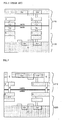
- FIG. 1 is a cross-sectional view of a conventional semiconductor device fabricated through a metal-to-metal bonding method.
- the semiconductor device of FIG. 1 is a part of an image sensor.
- the semiconductor device includes an upper wafer 110 and a lower wafer 120.
- the upper wafer 110 includes a photodiode PD to generate charges corresponding to the amount of light incident from the top and a floating diffusion FD to temporarily store the charges.
- the lower wafer 120 includes elements constituting the image sensor excluding the photodiode PD.
- A, B, D, and D represents regions in which a metal as a conductive material or polycrystalline silicon is formed.
- the regions A and C formed in the upper wafer 110 must be electrically connected to the regions B and D formed in the lower wafer 120, respectively.
- the top surface of a wafer is covered by an insulating material.
- the two wafers are electrically insulated from each other.
- conductive materials must be formed on the bonded portions of the two wafers. The conductive materials must be physically bonded to each other.
- a conductive material such as copper (Cu) may be formed on the surfaces of the regions A and C formed in the upper wafer 110 and the surfaces of the regions B and D formed in the lower wafer 120.
- the two wafers 110 and 120 are electrically connected to each other through the conductive layers formed on the surfaces of the regions A to D of the upper and lower wafers 110 and 120.
- the thickness of the wafers is inevitably increased.
- the lengths of wirings for electrical connection between elements formed in the two wafers 110 and 120 are increased.
- a power loss caused by resistance of the wirings cannot be ignored.
- an object of the present invention is to provide a method for electrically connecting wafers using a butting contact structure, which uses an oxide-to-oxide bonding method as a physical bonding process and uses a TSV or butting contact method as an electrical bonding process when bonding wafers, thereby simplifying additional processes.
- Another object of the present invention is to provide a semiconductor device which is fabricated through a method for electrically connecting wafers using a butting contact structure, which uses an oxide-to-oxide bonding method as a physical bonding process and uses a TSV or butting contact method as an electrical bonding process when bonding wafers, thereby simplifying additional processes
- a method for electrically connecting wafers which electrically connects first and second wafers subjected to a series of processes using a butting contact structure.
- the method includes: physically bonding the first and second wafers through an insulator-to-insulator bonding method; and electrically connecting a first conductive region of the first wafer to a second conductive region of the second wafer corresponding to the first conductive region through a metal-to-metal bonding method using through-silicon vias (TSVs) or butting contact holes.
- TSVs through-silicon vias
- a semiconductor device including first and second wafers which are electrically connected to each other.
- the first wafer includes one or more of a plurality of elements constituting a CMOS image sensor
- the second wafer includes a pixel driving circuit and the other elements of the plurality of elements constituting the CMOS image sensor excluding the elements formed in the first wafer.
- FIG. 2 is a cross-sectional view of a semiconductor device fabricated through a method for electrically connecting wafers according to an embodiment of the present invention.
- a physical bonding process for the semiconductor device according to the embodiment of the present invention is implemented through an oxide-to-oxide bonding method.
- the oxide-to-oxide bonding method upper and lower wafers 210 and 220 covered with oxide are physically bonded to each other.
- the two wafers 210 and 220 are electrically insulated from each other.
- this method is applied, only the alignment between the two wafers 210 and 220 may be considered.
- the bonding process may be relatively easily performed.
- FIG. 2 illustrates that the two wafers 210 and 220 are bonded to each other according to the oxide-to-oxide bonding method.
- the two wafers 210 and 220 may be bonded to each other through another bonding method, instead of the oxide-to-oxide bonding method.
- the bonded portion between the two wafers 110 and 120 is divided into the conductor (Cu) and the oxide.
- the entire bonded portion between the two wafers 210 and 220 is oxide.
- F represents a butting contact hole which is formed after physical bonding. The butting contact hole will be described below.
- First conductive regions A and C formed in the first wafer 210 are electrically connected to second conducive regions B and D formed in the second wafer 220 through first butting contact holes E formed in the first conductive regions A and C through the substrate of the first wafer 210 and second butting contact holes F formed between the first conductive regions A and C and the second conductive regions B and D, respectively.
- the first butting contact hole E is filled with an insulating material, and the second butting contact hole F is filled with a conductive material. Thus, only necessary parts may be electrically connected to each other.
- FIG. 2 illustrates the first butting contact hole E has a larger cross-sectional area than the second butting contact hole F.
- the first and second butting contact holes E and F may have the same cross-sectional area. Whether the first and second butting contact holes E and F are formed to have different cross-sectional areas or the same cross-sectional area is not a special technique for those skilled in the art. Thus, the detailed descriptions thereof are omitted herein.
- the following process may be commonly performed regardless of whether the first and second butting contact holes E and F have different cross-sectional areas or the same cross-sectional area: a photoresist is applied, a predetermined pattern formed in a mask is reflected onto the photoresist, and the photoresist is baked and then etched.
- FIGS. 3A to 3C are cross-sectional views illustrating a process for fabricating the semiconductor device of FIG. 2 .
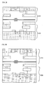
- FIG. 3A illustrates that two wafers are physically bonded to each other.
- FIG. 3B illustrates that the first butting contact hole is formed from the substrate of the first wafer to the first conductive region.
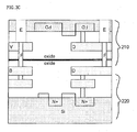
- FIG. 3C illustrates that the second butting contact hole is formed from the first conductive region to the second conductive region.
- oxides formed on the surfaces of the two wafers 210 and 220 are bonded to each other.
- this method is referred to as the oxide-to-oxide bonding method, and elements formed in the two wafers 210 and 220 are electrically insulated from each other.
- the first butting contact hole E is formed from the substrate of the first wafer 210 to the first conductive regions A and C. During this process, a patterned mask is used to form the first butting contact hole E through a photoresist process and an etch process.
- a substrate of a wafer in which semiconductor elements are formed has a considerably large thickness.
- the bottom of the substrate of the first wafer 210 is ground to make the thickness of the substrate smaller than the substrate (Si) of the second wafer 220.
- the substrate of the first wafer 210 at the bottom has a larger thickness than the substrate of the second wafer 220 at the top.
- the first butting contact hole E is formed through an etching process. Thus, as the thickness of the substrate to be etched is small, the etching time decreases.
- the time at which the thickness of the substrate of the first wafer 210 is adjusted may be adjusted.
- the process may be performed before the physical bonding process of FIG. 3A or may be performed before a process of FIG. 3B and after the physical bonding process of FIG. 3A .
- the second butting contact hole F is formed from the first conductive regions A and C to the second conductive regions B and D. During this process, a patterned mask is used to form the second butting hole F through a photoresist process and an etching process.
- the two butting contact holes E and F are formed to have different cross-sectional areas as illustrated in FIG. 3C , the first and second butting contact holes E and F may be easily distinguished from each other.
- the two butting contact holes E and F may be sequentially formed through the two processes.
- one butting contact hole including two butting contact holes E and F may be formed through one etching process.
- the process since the butting contact hole is formed through one process, the process may be simplified, and the process time may be reduced.
- through-silicon vias may be used instead of the butting contact holes.
- TSVs through-silicon vias
- a silicon wafer is divided into a plurality of chips having a thickness of several tens of micrometers, and the same chips are vertically stacked and connected through a through-electrode.
- This method has an advantage in that the thickness of chips and the power consumption may be reduced, compared to a conventional wire bonding method in which stacked chips are connected through a wire.
- the embodiment of the present invention may obtain the same effect even though any method is applied.
- the wafers are physically bonded to each other through the oxide-to-oxide bonding method which is simpler than the metal-to-metal bonding method, and then electrically connected to through TSVs or butting contact holes. Therefore, since the fabrication process may be simplified, a process error may be reduced, and the product yield may be improved.
Landscapes
- Wire Bonding (AREA)
- Internal Circuitry In Semiconductor Integrated Circuit Devices (AREA)
- Engineering & Computer Science (AREA)
- Manufacturing & Machinery (AREA)
- Solid State Image Pick-Up Elements (AREA)
Abstract
Description
- The present invention relates to a method for electrically connecting two wafers, and more particularly, to a method for electrically connecting wafers using a butting contact structure, which physically bonds two wafers according to an oxide-to-oxide bonding method and then electrically connects the two wafers using a butting contact structure.
- Recently, the process for reducing the physical size of an integrated circuit by reducing the sizes of devices on a wafer has reached the limit. In order to overcome such a limit, a method of vertically stacking two or more wafers has been proposed.
-
FIG. 1 is a cross-sectional view of a conventional semiconductor device fabricated through a metal-to-metal bonding method. - For convenience of description, suppose that the semiconductor device of
FIG. 1 is a part of an image sensor. The semiconductor device includes anupper wafer 110 and alower wafer 120. Theupper wafer 110 includes a photodiode PD to generate charges corresponding to the amount of light incident from the top and a floating diffusion FD to temporarily store the charges. Thelower wafer 120 includes elements constituting the image sensor excluding the photodiode PD. - Referring to
FIG. 1 , two wafers each having different elements implemented therein are bonded to each other. InFIG. 1 , A, B, D, and D represents regions in which a metal as a conductive material or polycrystalline silicon is formed. The regions A and C formed in theupper wafer 110 must be electrically connected to the regions B and D formed in thelower wafer 120, respectively. - When a semiconductor fabrication process is completed, the top surface of a wafer is covered by an insulating material. Thus, when the top surfaces of two wafers are physically bonded to each other, the two wafers are electrically insulated from each other. For this reason, in order to electrically connect two wafers, conductive materials must be formed on the bonded portions of the two wafers. The conductive materials must be physically bonded to each other.
- Referring to
FIG. 1 , a conductive material such as copper (Cu) may be formed on the surfaces of the regions A and C formed in theupper wafer 110 and the surfaces of the regions B and D formed in thelower wafer 120. - According to the above-described conventional metal-to-metal bonding method, the two
wafers lower wafers wafers - Furthermore, while each of the wafers is fabricated, the process of forming the conductive layer for electrical conduction must be separately performed during the bonding process. Thus, the time required for performing the process inevitably increases.
- Accordingly, the present invention has been made in an effort to solve the problems occurring in the related art, and an object of the present invention is to provide a method for electrically connecting wafers using a butting contact structure, which uses an oxide-to-oxide bonding method as a physical bonding process and uses a TSV or butting contact method as an electrical bonding process when bonding wafers, thereby simplifying additional processes.
- Another object of the present invention is to provide a semiconductor device which is fabricated through a method for electrically connecting wafers using a butting contact structure, which uses an oxide-to-oxide bonding method as a physical bonding process and uses a TSV or butting contact method as an electrical bonding process when bonding wafers, thereby simplifying additional processes
- In order to achieve the above object, according to one aspect of the present invention, there is provided a method for electrically connecting wafers, which electrically connects first and second wafers subjected to a series of processes using a butting contact structure. The method includes: physically bonding the first and second wafers through an insulator-to-insulator bonding method; and electrically connecting a first conductive region of the first wafer to a second conductive region of the second wafer corresponding to the first conductive region through a metal-to-metal bonding method using through-silicon vias (TSVs) or butting contact holes.
- According to another aspect of the present invention, there is provided a semiconductor device including first and second wafers which are electrically connected to each other. The first wafer includes one or more of a plurality of elements constituting a CMOS image sensor, and the second wafer includes a pixel driving circuit and the other elements of the plurality of elements constituting the CMOS image sensor excluding the elements formed in the first wafer.
- The above objects, and other features and advantages of the present invention will become more apparent after a reading of the following detailed description taken in conjunction with the drawings, in which:
-
FIG. 1 is a cross-sectional view of a conventional semiconductor device fabricated through a metal-to-metal bonding method; -
FIG. 2 is a cross-sectional view of a semiconductor device fabricated through a method for electrically connecting wafers according to an embodiment of the present invention; -
FIG. 3A illustrates that two wafers are physically bonded to each other; -
FIG. 3B illustrates that a first butting contact hole is formed from a substrate of a first wafer to a first conductive region; and -
FIG. 3C illustrates that a second butting contact hole is formed from the first conductive region to a second conductive region. - Reference will now be made in greater detail to a preferred embodiment of the invention, an example of which is illustrated in the accompanying drawings. Wherever possible, the same reference numerals will be used throughout the drawings and the description to refer to the same or like parts.
-
FIG. 2 is a cross-sectional view of a semiconductor device fabricated through a method for electrically connecting wafers according to an embodiment of the present invention. - Referring to
FIG. 2 , a physical bonding process for the semiconductor device according to the embodiment of the present invention is implemented through an oxide-to-oxide bonding method. According to the oxide-to-oxide bonding method, upper andlower wafers wafers wafers -
FIG. 2 illustrates that the twowafers - In the conventional semiconductor device of
FIG. 1 , the bonded portion between the twowafers FIG. 2 , however, the entire bonded portion between the twowafers FIG. 2 , F represents a butting contact hole which is formed after physical bonding. The butting contact hole will be described below. - First conductive regions A and C formed in the
first wafer 210 are electrically connected to second conducive regions B and D formed in thesecond wafer 220 through first butting contact holes E formed in the first conductive regions A and C through the substrate of thefirst wafer 210 and second butting contact holes F formed between the first conductive regions A and C and the second conductive regions B and D, respectively. - The first butting contact hole E is filled with an insulating material, and the second butting contact hole F is filled with a conductive material. Thus, only necessary parts may be electrically connected to each other.
-
FIG. 2 illustrates the first butting contact hole E has a larger cross-sectional area than the second butting contact hole F. However, the first and second butting contact holes E and F may have the same cross-sectional area. Whether the first and second butting contact holes E and F are formed to have different cross-sectional areas or the same cross-sectional area is not a special technique for those skilled in the art. Thus, the detailed descriptions thereof are omitted herein. - When the first and second butting contact holes E and F are formed, the following process may be commonly performed regardless of whether the first and second butting contact holes E and F have different cross-sectional areas or the same cross-sectional area: a photoresist is applied, a predetermined pattern formed in a mask is reflected onto the photoresist, and the photoresist is baked and then etched.
- Hereafter, a process for fabricating the semiconductor device of
FIG. 2 will be described. -
FIGS. 3A to 3C are cross-sectional views illustrating a process for fabricating the semiconductor device ofFIG. 2 . -
FIG. 3A illustrates that two wafers are physically bonded to each other. -
FIG. 3B illustrates that the first butting contact hole is formed from the substrate of the first wafer to the first conductive region. -
FIG. 3C illustrates that the second butting contact hole is formed from the first conductive region to the second conductive region. - Referring to
FIG. 3A , when twowafers wafers wafers - Referring to
FIG. 3B , the first butting contact hole E is formed from the substrate of thefirst wafer 210 to the first conductive regions A and C. During this process, a patterned mask is used to form the first butting contact hole E through a photoresist process and an etch process. - In general, a substrate of a wafer in which semiconductor elements are formed has a considerably large thickness. However, before the first butting contact hole E is formed, the bottom of the substrate of the
first wafer 210 is ground to make the thickness of the substrate smaller than the substrate (Si) of thesecond wafer 220. Referring toFIG. 2 , it can be seen that the substrate of thefirst wafer 210 at the bottom has a larger thickness than the substrate of thesecond wafer 220 at the top. The first butting contact hole E is formed through an etching process. Thus, as the thickness of the substrate to be etched is small, the etching time decreases. - The time at which the thickness of the substrate of the
first wafer 210 is adjusted may be adjusted. The process may be performed before the physical bonding process ofFIG. 3A or may be performed before a process ofFIG. 3B and after the physical bonding process ofFIG. 3A . - Referring to
FIG. 3C , the second butting contact hole F is formed from the first conductive regions A and C to the second conductive regions B and D. During this process, a patterned mask is used to form the second butting hole F through a photoresist process and an etching process. When the two butting contact holes E and F are formed to have different cross-sectional areas as illustrated inFIG. 3C , the first and second butting contact holes E and F may be easily distinguished from each other. - As described above, the two butting contact holes E and F may be sequentially formed through the two processes. However, when the two butting contact holes E and F do not need to have different cross-sectional areas, one butting contact hole including two butting contact holes E and F may be formed through one etching process. In this case, since the butting contact hole is formed through one process, the process may be simplified, and the process time may be reduced.
- In the present embodiment, through-silicon vias (TSVs) may be used instead of the butting contact holes. According to the TSV method, a silicon wafer is divided into a plurality of chips having a thickness of several tens of micrometers, and the same chips are vertically stacked and connected through a through-electrode. This method has an advantage in that the thickness of chips and the power consumption may be reduced, compared to a conventional wire bonding method in which stacked chips are connected through a wire.
- The embodiment of the present invention may obtain the same effect even though any method is applied.
- According to the embodiments of the present invention, the wafers are physically bonded to each other through the oxide-to-oxide bonding method which is simpler than the metal-to-metal bonding method, and then electrically connected to through TSVs or butting contact holes. Therefore, since the fabrication process may be simplified, a process error may be reduced, and the product yield may be improved.
- Although a preferred embodiment of the present invention has been described for illustrative purposes, those skilled in the art will appreciate that various modifications, additions and substitutions are possible, without departing from the scope and the spirit of the invention as disclosed in the accompanying claims.
Claims (10)
- A method for electrically connecting wafers, which electrically connects first and second wafers subjected to a series of processes using a butting contact structure, the method comprising:physically bonding the first and second wafers through an insulator-to-insulator bonding method; andelectrically connecting a first conductive region of the first wafer to a second conductive region of the second wafer corresponding to the first conductive region through a metal-to-metal bonding method using through-silicon vias (TSVs) or butting contact holes.
- The method of claim 1, wherein the electrically-connecting of the first conductive region of the first wafer to the second conductive region of the second wafer comprises:forming a butting contact hole to reach the second conductive region through the substrate bottom of the first wafer and the first conductive region;filling a conductive material into a part of the butting contact hole corresponding to the first conductive region and a region between the first and second conductive regions; andfilling an insulating material into the other part of the butting contact hole in which the conductive material is not filled.
- The method of claim 2, wherein the forming of the butting contact hole comprises:forming a first butting contact hole to reach the first conductive region through the substrate bottom of the first wafer; andforming a second butting contact hole to reach the second conductive region through the first conductive region.
- The method of claim 3, wherein the filling of the insulating material comprises filling an insulating material into the first butting contact hole, and
the filling of the conductive material comprises filling a conductive material into the second butting contact hole. - The method of claim 4, wherein the first butting contact hole has a larger cross-sectional area than the second butting contact hole.
- The method of claim 1, further comprising removing the substrate bottom of the first wafer to a predetermined thickness by grinding the substrate bottom of the first wafer.
- The method of claim 6, wherein the removing of the substrate bottom of the first wafer is performed before the physically-bonding of the first and second wafers or performed before the electrically-bonding of the first conductive region of the first wafer to the second conductive region of the second wafer after the physically-bonding of the first and second wafers.
- The method of claim 1, wherein the physically-bonding of the first and second wafers comprises physically bonding the first and second wafers through an oxide-to-oxide bonding method.
- A semiconductor device comprising first and second wafers which are electrically connected to each other through the method of claim 1,
wherein the first wafer comprises one or more of a plurality of elements constituting a CMOS image sensor, and
the second wafer comprises a pixel driving circuit and the other elements of the plurality of elements constituting the CMOS image sensor excluding the elements formed in the first wafer. - The semiconductor device of claim 9, wherein the first wafer comprises a photodiode to generate charges corresponding to incident light among the plurality of elements constituting the CMOS image sensor.
Applications Claiming Priority (1)
| Application Number | Priority Date | Filing Date | Title |
|---|---|---|---|
| KR1020120129899A KR101334220B1 (en) | 2012-11-16 | 2012-11-16 | Method for electric connecting the wafers using butting contact and semiconductor device manufactured by the method |
Publications (2)
| Publication Number | Publication Date |
|---|---|
| EP2733736A2 true EP2733736A2 (en) | 2014-05-21 |
| EP2733736A3 EP2733736A3 (en) | 2018-01-24 |
Family
ID=49680770
Family Applications (1)
| Application Number | Title | Priority Date | Filing Date |
|---|---|---|---|
| EP13005391.1A Withdrawn EP2733736A3 (en) | 2012-11-16 | 2013-11-15 | Method for electrically connecting wafers using butting contact struture and semiconductor device fabricated through the same |
Country Status (5)
| Country | Link |
|---|---|
| US (1) | US8906781B2 (en) |
| EP (1) | EP2733736A3 (en) |
| JP (1) | JP2014103395A (en) |
| KR (1) | KR101334220B1 (en) |
| CN (1) | CN103824867B (en) |
Families Citing this family (9)
| Publication number | Priority date | Publication date | Assignee | Title |
|---|---|---|---|---|
| CN105038120B (en) * | 2015-07-30 | 2018-03-16 | 浙江联诚氨基材料有限公司 | A kind of melamine resin |
| US20170062399A1 (en) * | 2015-08-24 | 2017-03-02 | Globalfoundries Inc. | Method and structure for low-k face-to-face bonded wafer dicing |
| CN106611756A (en) * | 2015-10-26 | 2017-05-03 | 联华电子股份有限公司 | Wafer-to-wafer butting structure and manufacturing method thereof |
| US9972603B2 (en) | 2015-12-29 | 2018-05-15 | Taiwan Semiconductor Manufacturing Co., Ltd. | Seal-ring structure for stacking integrated circuits |
| CN109285825B (en) * | 2017-07-21 | 2021-02-05 | 联华电子股份有限公司 | Chip stacking structure and manufacturing method of tube core stacking structure |
| CN107546174B (en) * | 2017-07-28 | 2020-07-17 | 中国科学院微电子研究所 | A process method for integrated circuit components |
| TWI905469B (en) * | 2017-10-30 | 2025-11-21 | 日商索尼半導體解決方案公司 | Solid-state imaging devices and electronic equipment |
| US10651153B2 (en) * | 2018-06-18 | 2020-05-12 | Intel Corporation | Three-dimensional (3D) memory with shared control circuitry using wafer-to-wafer bonding |
| US20230268372A1 (en) * | 2022-02-21 | 2023-08-24 | Taiwan Semiconductor Manufacturing Company, Ltd. | Stacked cmos image sensor |
Family Cites Families (10)
| Publication number | Priority date | Publication date | Assignee | Title |
|---|---|---|---|---|
| JP2617798B2 (en) * | 1989-09-22 | 1997-06-04 | 三菱電機株式会社 | Stacked semiconductor device and method of manufacturing the same |
| KR100604871B1 (en) * | 2004-06-17 | 2006-07-31 | 삼성전자주식회사 | Complementary nonvolatile memory device, operation method thereof, fabrication method thereof, logic device and semiconductor device including same |
| US7528494B2 (en) * | 2005-11-03 | 2009-05-05 | International Business Machines Corporation | Accessible chip stack and process of manufacturing thereof |
| US8158515B2 (en) * | 2009-02-03 | 2012-04-17 | International Business Machines Corporation | Method of making 3D integrated circuits |
| JP5985136B2 (en) * | 2009-03-19 | 2016-09-06 | ソニー株式会社 | SEMICONDUCTOR DEVICE, ITS MANUFACTURING METHOD, AND ELECTRONIC DEVICE |
| KR101648200B1 (en) * | 2009-10-22 | 2016-08-12 | 삼성전자주식회사 | Image sensor and method of manufacturing the same |
| US8159060B2 (en) * | 2009-10-29 | 2012-04-17 | International Business Machines Corporation | Hybrid bonding interface for 3-dimensional chip integration |
| US20120248621A1 (en) * | 2011-03-31 | 2012-10-04 | S.O.I.Tec Silicon On Insulator Technologies | Methods of forming bonded semiconductor structures, and semiconductor structures formed by such methods |
| US8957358B2 (en) * | 2012-04-27 | 2015-02-17 | Taiwan Semiconductor Manufacturing Company, Ltd. | CMOS image sensor chips with stacked scheme and methods for forming the same |
| US8563403B1 (en) * | 2012-06-27 | 2013-10-22 | International Business Machines Corporation | Three dimensional integrated circuit integration using alignment via/dielectric bonding first and through via formation last |
-
2012
- 2012-11-16 KR KR1020120129899A patent/KR101334220B1/en active Active
-
2013
- 2013-11-13 US US14/079,075 patent/US8906781B2/en active Active
- 2013-11-14 JP JP2013235660A patent/JP2014103395A/en active Pending
- 2013-11-15 CN CN201310573253.3A patent/CN103824867B/en active Active
- 2013-11-15 EP EP13005391.1A patent/EP2733736A3/en not_active Withdrawn
Non-Patent Citations (1)
| Title |
|---|
| None |
Also Published As
| Publication number | Publication date |
|---|---|
| CN103824867B (en) | 2017-03-01 |
| EP2733736A3 (en) | 2018-01-24 |
| JP2014103395A (en) | 2014-06-05 |
| US8906781B2 (en) | 2014-12-09 |
| US20140138847A1 (en) | 2014-05-22 |
| CN103824867A (en) | 2014-05-28 |
| KR101334220B1 (en) | 2013-11-29 |
Similar Documents
| Publication | Publication Date | Title |
|---|---|---|
| US8906781B2 (en) | Method for electrically connecting wafers using butting contact structure and semiconductor device fabricated through the same | |
| TWI746776B (en) | Semiconductor device and method for manufacturing the same | |
| US9748304B2 (en) | Image sensor devices, methods of manufacture thereof, and semiconductor device manufacturing methods | |
| KR101729378B1 (en) | Semiconductor devices and methods of manufacture thereof | |
| KR101763022B1 (en) | Hybrid bond pad structure | |
| CN103811506B (en) | Integrated circuit (IC) system, imaging sensor system and preparation method thereof | |
| US8836137B2 (en) | Method for creating a 3D stacked multichip module | |
| EP2648215A2 (en) | Method and apparatus providing integrated circuit system with interconnected stacked device wafers | |
| US9559135B2 (en) | Conduction layer for stacked CIS charging prevention | |
| CN110610923B (en) | Semiconductor device, semiconductor package, and method for manufacturing semiconductor device | |
| US9257392B2 (en) | Semiconductor package with through silicon via interconnect | |
| CN111092090B (en) | Integrated chip and forming method thereof | |
| KR102576062B1 (en) | A semiconductor device having a through silicon via and method of manufacturing the same | |
| KR20130053338A (en) | Integrated circuit device having through silicon via structure | |
| KR20150043933A (en) | Integrated circuit device having through-silicon via structure and method of manufacturing the same | |
| CN101312181B (en) | semiconductor chip, integrated circuit structure and semiconductor wafer | |
| EP2672511B1 (en) | 3d stacked multichip module and method of fabrication | |
| CN111244057A (en) | Bonding structure and manufacturing method thereof | |
| CN109103169B (en) | Semiconductor device with a semiconductor layer having a plurality of semiconductor layers | |
| KR101132852B1 (en) | Pixel array and image sensor including the same | |
| JP2010205921A (en) | Semiconductor apparatus, and method of manufacturing semiconductor apparatus | |
| US10734339B2 (en) | Bond pad structure for bonding improvement | |
| US20180108540A1 (en) | Method of forming an interposer and a method of manufacturing a semiconductor package including the same | |
| TWI529872B (en) | Radio frequency device package and manufacturing method thereof | |
| CN106409813B (en) | Multicomponent packaging body and preparation method thereof |
Legal Events
| Date | Code | Title | Description |
|---|---|---|---|
| PUAI | Public reference made under article 153(3) epc to a published international application that has entered the european phase |
Free format text: ORIGINAL CODE: 0009012 |
|
| 17P | Request for examination filed |
Effective date: 20131115 |
|
| AK | Designated contracting states |
Kind code of ref document: A2 Designated state(s): AL AT BE BG CH CY CZ DE DK EE ES FI FR GB GR HR HU IE IS IT LI LT LU LV MC MK MT NL NO PL PT RO RS SE SI SK SM TR |
|
| AX | Request for extension of the european patent |
Extension state: BA ME |
|
| RAP1 | Party data changed (applicant data changed or rights of an application transferred) |
Owner name: SK HYNIX INC. |
|
| PUAL | Search report despatched |
Free format text: ORIGINAL CODE: 0009013 |
|
| AK | Designated contracting states |
Kind code of ref document: A3 Designated state(s): AL AT BE BG CH CY CZ DE DK EE ES FI FR GB GR HR HU IE IS IT LI LT LU LV MC MK MT NL NO PL PT RO RS SE SI SK SM TR |
|
| AX | Request for extension of the european patent |
Extension state: BA ME |
|
| RIC1 | Information provided on ipc code assigned before grant |
Ipc: H01L 23/48 20060101ALI20171219BHEP Ipc: H01L 21/768 20060101ALN20171219BHEP Ipc: H01L 21/60 20060101AFI20171219BHEP Ipc: H01L 27/146 20060101ALI20171219BHEP Ipc: H01L 21/822 20060101ALN20171219BHEP |
|
| STAA | Information on the status of an ep patent application or granted ep patent |
Free format text: STATUS: THE APPLICATION IS DEEMED TO BE WITHDRAWN |
|
| 18D | Application deemed to be withdrawn |
Effective date: 20180725 |