EP2733525A1 - Display module with green colour filter and matched light source - Google Patents
Display module with green colour filter and matched light source Download PDFInfo
- Publication number
- EP2733525A1 EP2733525A1 EP13190977.2A EP13190977A EP2733525A1 EP 2733525 A1 EP2733525 A1 EP 2733525A1 EP 13190977 A EP13190977 A EP 13190977A EP 2733525 A1 EP2733525 A1 EP 2733525A1
- Authority
- EP
- European Patent Office
- Prior art keywords
- light source
- spectrum
- wavelength
- energy
- filter layer
- Prior art date
- Legal status (The legal status is an assumption and is not a legal conclusion. Google has not performed a legal analysis and makes no representation as to the accuracy of the status listed.)
- Withdrawn
Links
Images



Classifications
-
- G—PHYSICS
- G02—OPTICS
- G02F—OPTICAL DEVICES OR ARRANGEMENTS FOR THE CONTROL OF LIGHT BY MODIFICATION OF THE OPTICAL PROPERTIES OF THE MEDIA OF THE ELEMENTS INVOLVED THEREIN; NON-LINEAR OPTICS; FREQUENCY-CHANGING OF LIGHT; OPTICAL LOGIC ELEMENTS; OPTICAL ANALOGUE/DIGITAL CONVERTERS
- G02F1/00—Devices or arrangements for the control of the intensity, colour, phase, polarisation or direction of light arriving from an independent light source, e.g. switching, gating or modulating; Non-linear optics
- G02F1/01—Devices or arrangements for the control of the intensity, colour, phase, polarisation or direction of light arriving from an independent light source, e.g. switching, gating or modulating; Non-linear optics for the control of the intensity, phase, polarisation or colour
- G02F1/13—Devices or arrangements for the control of the intensity, colour, phase, polarisation or direction of light arriving from an independent light source, e.g. switching, gating or modulating; Non-linear optics for the control of the intensity, phase, polarisation or colour based on liquid crystals, e.g. single liquid crystal display cells
- G02F1/133—Constructional arrangements; Operation of liquid crystal cells; Circuit arrangements
- G02F1/1333—Constructional arrangements; Manufacturing methods
- G02F1/1335—Structural association of cells with optical devices, e.g. polarisers or reflectors
- G02F1/133509—Filters, e.g. light shielding masks
- G02F1/133514—Colour filters
-
- H—ELECTRICITY
- H10—SEMICONDUCTOR DEVICES; ELECTRIC SOLID-STATE DEVICES NOT OTHERWISE PROVIDED FOR
- H10K—ORGANIC ELECTRIC SOLID-STATE DEVICES
- H10K59/00—Integrated devices, or assemblies of multiple devices, comprising at least one organic light-emitting element covered by group H10K50/00
- H10K59/30—Devices specially adapted for multicolour light emission
- H10K59/38—Devices specially adapted for multicolour light emission comprising colour filters or colour changing media [CCM]
-
- G—PHYSICS
- G02—OPTICS
- G02F—OPTICAL DEVICES OR ARRANGEMENTS FOR THE CONTROL OF LIGHT BY MODIFICATION OF THE OPTICAL PROPERTIES OF THE MEDIA OF THE ELEMENTS INVOLVED THEREIN; NON-LINEAR OPTICS; FREQUENCY-CHANGING OF LIGHT; OPTICAL LOGIC ELEMENTS; OPTICAL ANALOGUE/DIGITAL CONVERTERS
- G02F1/00—Devices or arrangements for the control of the intensity, colour, phase, polarisation or direction of light arriving from an independent light source, e.g. switching, gating or modulating; Non-linear optics
- G02F1/01—Devices or arrangements for the control of the intensity, colour, phase, polarisation or direction of light arriving from an independent light source, e.g. switching, gating or modulating; Non-linear optics for the control of the intensity, phase, polarisation or colour
- G02F1/13—Devices or arrangements for the control of the intensity, colour, phase, polarisation or direction of light arriving from an independent light source, e.g. switching, gating or modulating; Non-linear optics for the control of the intensity, phase, polarisation or colour based on liquid crystals, e.g. single liquid crystal display cells
- G02F1/133—Constructional arrangements; Operation of liquid crystal cells; Circuit arrangements
- G02F1/1333—Constructional arrangements; Manufacturing methods
- G02F1/1335—Structural association of cells with optical devices, e.g. polarisers or reflectors
- G02F1/1336—Illuminating devices
- G02F1/133624—Illuminating devices characterised by their spectral emissions
Definitions
- the invention relates in general to a display module, and more particularly to a display module capable of resolving the leaking problem of a green filter layer in a red light region.
- CF color filter
- the LCD being a non-active light-emitting element, firstly uses an internal backlight unit or an external ambient light (a reflective or semi- transmitting LCD) as the light source, uses a driving circuit to control liquid crystal molecules to form grey scale display, provides colors through the red(R)/green(G)/blue(B) filter layers of the color filter, and adjusts the RGB ratios, such that a color display frame can be displayed in a full-color mode.
- an internal backlight unit or an external ambient light a reflective or semi- transmitting LCD
- each color filter allows only the light whose wavelength belongs to a specific range to pass through.
- Light leak occurs when the wavelength of the light passing through the color filter is outside the specific range.
- the occurrence of light leak affects the chromaticity coordinates of the white or RGB dots, and accordingly deteriorates the display effect and quality.
- the color filters currently available still cannot achieve the ideal state of having no leaking of the light of other colors, and cannot meet the market demand and future trend.
- the invention is directed to a display module capable of reducing the leaking problem of a green filter layer by controlling a ratio between the spectrums of a light source and the green filter layer within different wavelength intervals.
- a display module having a light source has a normalized emission spectrum.
- the display module comprises a display unit.
- the display unit comprises a first substrate, a second substrate opposite to the first substrate, a display medium and a green filter layer.
- the display medium is disposed between the first substrate and the second substrate.
- the green filter layer is disposed on the first substrate or the second substrate, and has a normalized transmission spectrum.
- a product of an emission value corresponding to a maximum peak wavelength of the normalized emission spectrum between 480nm and 660nm of wavelength of the light source and a transmission value of the normalized transmission spectrum of the green filter layer corresponding to the maximum peak wavelength is a first product value.
- a product of an illumination intensity of the emission spectrum and a transmittance intensity of the transmission spectrum corresponding to a cross-point between the emission spectrum and the transmission spectrum between 660nm and 780nm of wavelength is a second product value.
- a ratio of the second product value to the first product value is less than 2%.
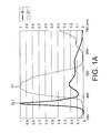
- FIG. 1A shows a schematic diagram of a normalized emission spectrum of a light source and a normalized transmission spectrum of a green filter layer
- FIG. 1B shows a diagram of an multiplication spectrum of a relative transmission energy of the light source of FIG. 1A passing through a green filter layer and a liquid crystal;
- FIG. 2 shows a schematic diagram of a normalized emission spectrum of a light source and a normalized transmission spectrum of a green filter layer
- FIG. 3 shows a schematic diagram of a normalized emission spectrum of a red light of a light source and a normalized transmission spectrum of a green filter layer according to an embodiment of the invention
- FIG. 4 shows a schematic diagram of a normalized emission spectrum of a red light region of a light source and a normalized transmission spectrum of a green filter layer according to an embodiment of the invention
- FIG. 5 shows a schematic diagram of a normalized emission spectrum of a red light of a light source and a normalized transmission spectrum of a green filter layer according to an embodiment of the invention
- FIG. 6 shows a schematic diagram of an organic light emitting diode (OLED) display module according to an embodiment of the invention
- FIG. 7 shows a structural diagram of a liquid crystal display module (LCD) according to an embodiment of the invention.
- FIG. 1A shows a schematic diagram of a normalized emission spectrum of a light source and a normalized transmission spectrum of a green filter layer.
- the emission spectrum of the light source is denoted by a curve BL1.
- a horizontal axis of the diagram corresponds to an emission wavelength of the visible light of the light source as nanometer (nm) which is a unit of wavelength.
- the wavelength of the spectrum of the visible light is between 380nm and 780nm.
- a left-side vertical axis of the diagram corresponds to the illumination intensity of the light source.
- the illumination intensity (in an arbitrary unit) is shown by a relative value based on the maximum value as 1.
- the light source has a blue light region, a green light region, and a red light region (not illustrated) in sequence in a direction from short wavelength to long wavelength.
- a curve G1 denotes a normalized transmission spectrum of the green filter layer.
- a horizontal axis of FIG. 1A corresponds to the wavelength range of the visible light able to pass through the green filter layer. The unit of the wavelength is nm.
- a right-side vertical axis corresponds to the transmission rate of the light able to pass through the green filter layer. The transmission rate (in an arbitrary unit) is shown by a relative value based on the maximum value as 1.
- FIG. 1B shows a diagram of a multiplication spectrum of a relative transmission energy of the light source of FIG. 1A passing through the green filter layer and a liquid crystal.
- An integral area of the multiplication spectrum C of FIG. 1B over the wavelength interval of the visible light is a transmission energy of the light source passing through the green filter layer and the liquid crystal.
- FIG. 1B there is a transmitting light of the red light region between 660nm and 780nm of wavelength. Therefore, it is known that when the green filter layer is used, there is an existence of the transmitting light in the red light region between 660nm and 780nm of wavelength.
- FIG. 1B is exemplified by an LCD display in which a display medium providing grey scales is a liquid crystal material.
- an OLED display in which an OLED emits a white light and is functioned as a display medium providing grey scales and a light source at the same time, is used, there is still a transmitting light in the red light region between 660nm and 780nm of wavelength after the light source passes through the green filter layer.
- no matter what type of display is used there is a transmitting light in the red light region between 660nm and 780nm of wavelength as long as the display is used in incorporated with the green filter layer. If the light source has the transmitting light in the red light region passing through the green filter layer, chromaticity coordinates of white dots will be affected.
- the energy of the light source between 380nm and 780nm of wavelength passing through the green filter layer is defined as a first energy.
- the energy of the light source in the red light region between 660nm and 780nm passing through the green filter layer is defined as a second energy. That is, the first energy is the integral area of the multiplication spectrum C over the wavelength between 380nm and 780nm, and the second energy is the integral area of the multiplication spectrum C over the wavelength between 660nm and 780nm. If the ratio of the second energy to the first energy can be lowered, the displacement in the chromaticity coordinates of white dots will be reduced.
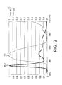
- FIG. 2 shows a schematic diagram of a normalized emission spectrum of the light source and a normalized transmission spectrum of the green filter layer.
- a curve BL2 denotes an emission spectrum of the light source.
- the emission spectrum is measured by using three diffusion sheets disposed in the backlight unit.
- the horizontal axis corresponds to the emission wavelength of the light source (the unit of the wavelength is nm)
- the left-side vertical axis of FIG. 2 corresponds to the illumination intensity of the light source.
- the illumination intensity (in an arbitrary unit) is shown by a relative value based on the maximum value is 1.
- a curve G2 denotes a transmission spectrum of the green filter layer
- the horizontal axis corresponds to the wavelength range of the light (the unit is nm) able to pass through the green filter layer.
- the right-side vertical axis corresponds to the transmission rate of the green filter layer for the light.
- the transmission rate (in an arbitrary unit) is a relative value based on the maximum value is 1.
- the overlapping part between the transmission spectrum G2 of the green filter layer and the emission spectrum BL2 of the light source is the part of the entire emission area of the visible light of the light source that will pass through the green filter layer.
- the transmission spectrum G2 of the green filter layer partly overlaps the emission spectrum BL2 of the light source (as indicated by the slashed area in FIG. 2 ). This area is the part that the light source of the red light region will pass through the green filter layer, and is an area in which red light leaks.
- BLU ( ⁇ ) denotes the emission spectrum of the light source.
- GCF ( ⁇ ) denotes the transmission spectrum of the green filter layer.
- CELL ( ⁇ ) denotes the total transmission spectrum of the remaining part of the display unit exclusive of the photoresist material (such as CF).
- the emission energy G can be obtained by bringing wavelengths of a particular light band to the upper limit and the lower limit of the integral formula.
- the range of the slashed area must be reduced, that is, the overlapping part between the emission spectrum of the light source and the green filter layer in the red light region must be reduced.
- the above formula is exemplified by the use of LCD display. It can be understood that when the OLED, which emits a white light, is used as the light source, the energy integral formula is an multiplication integral of the emission spectrum of the light source and the transmission spectrum of the green filter layer.
- the energy G total denoting the light energy of the light source passing through the green filter layer is the first energy.
- the energy GR leakage denoting the light energy of the light source passing through the green filter layer is the second energy. Therefore, if the overlapping between the emission spectrum BL2 of the light source and the transmission spectrum G2 of the green filter layer in the red light region can be reduced, the ratio of the second energy to the first energy can be reduced accordingly.
- the overlapping part between the emission spectrum of the light source and the transmission spectrum of the green filter layer between 660nm and 780nm can be reduced by adjusting the kinds and composition ratio of materials of the light source in the red light region of the emission spectrum, to reduce the ratio of the second energy to the first energy, to reduce the transmittance intensity of the light source with respect to the green filter layer within the wavelength between 660nm and 780nm.
- the light source of the red light region can be generated by a group consisting of a red fluorescent powder, a red light emitting diode chip, a red quantum dot, an OLED and a combination thereof.
- the red fluorescent powder may comprise sulfide, nitride or silicide. The material type or composition ratio of the fluorescent powder can be adjusted.
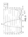
- FIG. 3 shows a schematic diagram of a normalized emission spectrum (corresponding to the left side vertical axis) of the light source of the red light region and a normalized transmission spectrum (corresponding to the right side vertical axis) of the green filter layer according to an embodiment of the invention.
- a curve R1 is the emission spectrum of the ordinary light source of the red light region indicated in FIG. 2 .
- a curve R2 is the emission spectrum of the light source in the red light region using sulfide type fluorescent powder. As indicated in FIG. 3 , the full width at half maximum (FWHM) of the emission spectrum of the curve R2 is less than that of the curve R1.
- the positions of peaks of the curves R2 and R1 can be the same, and the invention is not limited thereto.
- the ratio of the second energy (between 660nm and 780nm of wavelength) to the first energy (between 380nm and 780nm of wavelength) is about 2.87%, obtained according to an overlapping percentage between the the curve R1 and the transmission spectrum G2 of the green filter layer.
- the ratio of the second energy (between 660nm and 780nm of wavelength) to the first energy (between 380nm and 780nm of wavelength) is about 1.2%, obtained according to an overlapping percentage between the the curve R2 and the transmission spectrum G2 of the green filter layer.
- the overlapping percentage between the emission spectrum of the curve R1 and the transmission spectrum G2 of the green filter layer drops by 1.67%. That is, the light leak is reduced by 58%, largely reducing the problem of red light leak occurring to the green filter layer in the red light region. Therefore, by adjusting the material type or ingredient percentages of the light source providing the red light, the ratio of the second energy to the first energy can be reduced to be less than 2%. Preferably, the ratio of the second energy to the first energy is reduced to be less than 1%.
- FIG. 4 shows a schematic diagram of a normalized emission spectrum (corresponding to the left side vertical axis) of the light source of the red light region and a normalized transmission spectrum (corresponding to the right side vertical axis) of the green filter layer according to an embodiment of the invention.
- the curve G2 is a transmission spectrum of the green filter layer shown in FIG. 2 .
- the curve R1 is an emission spectrum of the ordinary light source of the red light region shown in FIG. 2 .
- a curve R3 is an emission spectrum of the light source using nitride fluorescent powder and has a main peak corresponding to a wavelength of 620nm. In comparison to the main peak of the curve R1, the peak of the curve 3 is displaced towards the short wavelength area (leftward displacement).
- the ratio of the second energy (between 660nm and 780nm of wavelength) to the first energy (between 380nm and 780nm of wavelength) is about 1.3%, obtained according to the overlapping percentage between the emission spectrum of the curve R3 and the transmission spectrum G2 of the green filter layer represented by.
- the overlapping percentage between the emission spectrum of the curve R1 and the transmission spectrum G2 of the green filter layer (2.87%) shown in FIG. 4 and the overlapping percentage between the emission spectrum of the curve R3 and the transmission spectrum G2 of the green filter layer (1.3%) drops by 1.57%. That is, the light leak is reduced by 55%, largely reducing the problem of red light leak occurring to the green filter layer in the red light region.
- the ratio of the second energy to the first energy can be reduced to be less than 2%.
- the ratio of the second energy to the first energy is reduced to be less than 1%.
- FIG. 5 shows a schematic diagram of a normalized emission spectrum of the light source and a normalized transmission spectrum of the green filter layer according to an embodiment of the invention.
- a curve G3 denotes the normalized transmission spectrum of the green filter layer according to an embodiment of the invention.
- a curve BL3 denotes a normalized emission spectrum of the light source according to an embodiment of the invention.
- the emission spectrum and the transmission spectrum are illustrated in the same spectrum diagram according to the Cartesian coordinates, such that the emission spectrum and the transmission spectrum can use the same coordinate ranges in the x-axis and the y-axis. As indicated in the spectrum diagram of FIG.
- the horizontal axis corresponds to the wavelength of the light able to pass through the green filter layer and the emission wavelength of the light source (the unit is nm).
- the vertical axis corresponds to the normalized transmission rate of the wavelength of the light able to pass through the green filter layer.
- the value of the vertical axis is an arbitrary unit.
- the emission spectrum (curve BL3) of the light source may comprise a blue light region, a green light region and a red light region for providing a blue light region, a green light region and a red light region, respectively.
- the red light region can be generated by a group consisting of a red fluorescent powder, a red light emitting diode chip, a red quantum dot, an OLED or a combination thereof.
- the red fluorescent powder may comprise nitride, such as a nitride whose light emitting peak corresponds to a wavelength between 600nm and 630nm (such as 620nm), or a material whose emission spectrum of red light region has narrower full width at half maximum, such as sulfide.
- the product of the maximum peak value BL3a of the normalized emission spectrum BL3 of the light source corresponding to a wavelength ⁇ a, and the transmittance intensity value G3a of the normalized transmission spectrum G3 of the green filter layer corresponding to the wavelength ⁇ a is a first product value.
- the product of the illumination intensity value BL3b of the normalized emission spectrum BL3 and the transmittance intensity value G3b of the normalized transmission spectrum G3, corresponding to a cross-point between the normalized emission spectrum BL3 and the normalized transmission spectrum G3, is a second product value.
- the ratio of the second product value to the first product value is less than 2%.
- the ratio of the second product value to the first product value is reduced to be less than 1%.
- the maximum emission peak value of the normalized emission spectrum BL3 is 0.22
- the transmittance intensity value of the normalized transmission spectrum G3 corresponding to the wavelength value corresponding to the maximum emission peak value is 0.97
- the first product value is 0.2134.
- the illumination intensity value of the normalized emission spectrum BL3 corresponding to a cross-point between the normalized emission spectrum and the normalized transmission spectrum is 0.06
- the transmittance intensity value of the normalized transmission spectrum G3 corresponding to the cross-point is 0.06, so that the second product value is 0.0036.
- the ratio of the second product value to the first product value is 1.69% which is less than 2%.
- the ratio of the second product value to the first product value is preferably less than 1%, by adjusting the material types and ingredient percentage of the red fluorescent powder, the red light emitting diode chip, the red quantum dot, or the OLED used in the light source to make the peak of the red light region have narrower full width at half maximum or shift the peak towards short wavelength.
- the ratio of the second product value to the first product value is less than 1%, by adjusting the ingredients of sulfide, nitride or silicide of the red fluorescent powder to shift the peak of the red light region towards short wavelength.
- the OLED display module 1 comprises a display unit 10.
- the display unit 10 comprises a first substrate 100, a color filter layer 102, an organic light emitting unit 104, and a second substrate 120.
- the organic light emitting unit 104 is disposed between the first substrate 100 and the second substrate 120.
- the color filter layer 102 is disposed on the first substrate 100, and may comprise a blue filter layer, a green filter layer and a red filter layer.
- the color filter layer 102 can be disposed on the second substrate 120 according to the viewer's position, and the invention is not limited thereto.
- the organic light emitting unit 104 is the display medium providing grey scales and the light source at the same time.
- the light source generated by the organic light emitting unit 104 may comprise several spectrum regions of different colors, such as a blue light region, a green light region and a red light region, corresponding to the transmission spectrum of the blue light emitting unit, the transmission spectrum of the green light emitting unit and the transmission spectrum of the red light emitting unit, respectively.
- the light of different regions can be provided by different elements or materials.
- the light of the blue light region can be provided by a blue LED
- the light of the red region can be provided by an OLED, and the invention is not limited thereto.
- Suitable design can be used as long as the emission spectrum of the light source and the transmission spectrum of the green filter layer are conformed to the ratio of the second energy to the first energy being less than 2% as indicated in FIG. 3 ⁇ 4 or are conformed to the ratio of the second energy to the first energy being less than 2% as indicated in FIG. 5 .
- FIG. 7 a structural diagram of a liquid crystal display (LCD) module 2 according to an embodiment of the invention is shown.
- the liquid crystal display module 2 comprises a display unit 20 and a backlight unit 25.
- FIG. 7 only illustrates a first substrate 200, a color filter layer 202, a liquid crystal molecule layer 204 and a second substrate 220 of the display unit 20, and other elements (such as electrodes) are omitted, for easy explanation for embodiments.
- the color filter layer 202 is disposed on the first substrate 200.
- the color filter layer 202 may also be disposed on the second substrate 220, such as color filters on a thin film transistor array substrate (COA).
- COA thin film transistor array substrate
- the backlight unit 25 is used for providing the light source comprising several spectrum regions of different colors, such as a blue light region, a green light region and a red light region.
- the backlight unit 25 can be implemented in different ways for providing the light source.
- the backlight unit 25 can be implemented by packaging the red and the green fluorescent powders and the blue light emitting diode (LED) together, or packaging the YAG fluorescent powder and the blue LED together.
- the emission spectrum of the light source may comprise several regions of different colors (such as a blue light region, a green light region and a red light region).
- the red light region can be generated by a group consisting of a red fluorescent powder, a red light emitting diode chip, a red quantum dot, an OLED or a combination thereof.
- the red fluorescent powder comprises sulfide.
- the material of the red light emitting unit can be designed to have a nitride whose light emitting peak is between 600nm and 630nm (such as 620nm) of wavelength.
- the types of the blue light emitting unit and the green light emitting unit can be different from that of the red light emitting unit, and the invention is not limited thereto.
- the red light emitting unit can be realized by an OLED
- the blue light emitting unit and the green light emitting unit can be realized by an LED.
- the red light region and the green filter layer of the backlight unit 25 are conformed to the design of the ratio of the second energy to the first energy being less than 2% as indicated in FIG. 4 ⁇ 5 or are conformed to the design of the ratio of the second energy to the first energy being less than 2% as indicated in FIG. 5 .
- the display module 1 and the display module 2 may further comprise a touch unit (not illustrated).
- the touch design of the touch unit comprises a touch sensing circuit (not illustrated) and may integrated with one of the substrates of the above embodiments.
- the present embodiment uses the in-cell or the on-cell touch technology, such as the in-cell photo technology, the in-cell capacitive technology, the in-cell resistive technology and the on-cell capacitive technology, for touch sensing control.
- the touch sensing circuit can be realized by a multi-touch sensing circuit, and the invention is not limited thereto.
- the display module of the above embodiments of the invention can effectively control the percentage of red light leak and reduce the red light leak which occurs when the light of the light source passes through a green filter layer, such that the display module has better display quality.
Landscapes
- Physics & Mathematics (AREA)
- Nonlinear Science (AREA)
- Mathematical Physics (AREA)
- Chemical & Material Sciences (AREA)
- Crystallography & Structural Chemistry (AREA)
- General Physics & Mathematics (AREA)
- Optics & Photonics (AREA)
- Electroluminescent Light Sources (AREA)
- Devices For Indicating Variable Information By Combining Individual Elements (AREA)
- Liquid Crystal (AREA)
Abstract
Description
- The invention relates in general to a display module, and more particularly to a display module capable of resolving the leaking problem of a green filter layer in a red light region.
- Along with the advance in technology, display products have become popular in people's daily life. Display products generate bright colors through the use of a color filter (CF) which filters off the light of the light source and displays the desired quality of colors.
- Let the liquid crystal display (LCD) be taken for example. The LCD, being a non-active light-emitting element, firstly uses an internal backlight unit or an external ambient light (a reflective or semi- transmitting LCD) as the light source, uses a driving circuit to control liquid crystal molecules to form grey scale display, provides colors through the red(R)/green(G)/blue(B) filter layers of the color filter, and adjusts the RGB ratios, such that a color display frame can be displayed in a full-color mode.
- As the markets have strong demand for high resolution and high contrast display products, the color filter has become a crucial factor to the colorization effect of the LCD. In an ideal color filter, each color filter allows only the light whose wavelength belongs to a specific range to pass through. Light leak occurs when the wavelength of the light passing through the color filter is outside the specific range. The occurrence of light leak affects the chromaticity coordinates of the white or RGB dots, and accordingly deteriorates the display effect and quality. However, due to the material characteristics, the color filters currently available still cannot achieve the ideal state of having no leaking of the light of other colors, and cannot meet the market demand and future trend.
- The invention is directed to a display module capable of reducing the leaking problem of a green filter layer by controlling a ratio between the spectrums of a light source and the green filter layer within different wavelength intervals.
- According to one embodiment of the present invention, a display module having a light source is disclosed. The light source has a normalized emission spectrum. The display module comprises a display unit. The display unit comprises a first substrate, a second substrate opposite to the first substrate, a display medium and a green filter layer. The display medium is disposed between the first substrate and the second substrate. The green filter layer is disposed on the first substrate or the second substrate, and has a normalized transmission spectrum. A product of an emission value corresponding to a maximum peak wavelength of the normalized emission spectrum between 480nm and 660nm of wavelength of the light source and a transmission value of the normalized transmission spectrum of the green filter layer corresponding to the maximum peak wavelength is a first product value. A product of an illumination intensity of the emission spectrum and a transmittance intensity of the transmission spectrum corresponding to a cross-point between the emission spectrum and the transmission spectrum between 660nm and 780nm of wavelength is a second product value. A ratio of the second product value to the first product value is less than 2%.
- The above and other aspects of the invention will become better understood with regard to the following detailed description of the preferred but non-limiting embodiment (s). The following description is made with reference to the accompanying drawings.
-
FIG. 1A shows a schematic diagram of a normalized emission spectrum of a light source and a normalized transmission spectrum of a green filter layer; -
FIG. 1B shows a diagram of an multiplication spectrum of a relative transmission energy of the light source ofFIG. 1A passing through a green filter layer and a liquid crystal; -
FIG. 2 shows a schematic diagram of a normalized emission spectrum of a light source and a normalized transmission spectrum of a green filter layer; -
FIG. 3 shows a schematic diagram of a normalized emission spectrum of a red light of a light source and a normalized transmission spectrum of a green filter layer according to an embodiment of the invention; -
FIG. 4 shows a schematic diagram of a normalized emission spectrum of a red light region of a light source and a normalized transmission spectrum of a green filter layer according to an embodiment of the invention; -
FIG. 5 shows a schematic diagram of a normalized emission spectrum of a red light of a light source and a normalized transmission spectrum of a green filter layer according to an embodiment of the invention; -
FIG. 6 shows a schematic diagram of an organic light emitting diode (OLED) display module according to an embodiment of the invention; -
FIG. 7 shows a structural diagram of a liquid crystal display module (LCD) according to an embodiment of the invention. -
FIG. 1A shows a schematic diagram of a normalized emission spectrum of a light source and a normalized transmission spectrum of a green filter layer. Referring toFIG. 1A , the emission spectrum of the light source is denoted by a curve BL1. A horizontal axis of the diagram corresponds to an emission wavelength of the visible light of the light source as nanometer (nm) which is a unit of wavelength. The wavelength of the spectrum of the visible light is between 380nm and 780nm. A left-side vertical axis of the diagram corresponds to the illumination intensity of the light source. The illumination intensity (in an arbitrary unit) is shown by a relative value based on the maximum value as 1. The light source has a blue light region, a green light region, and a red light region (not illustrated) in sequence in a direction from short wavelength to long wavelength. - In
FIG. 1A , a curve G1 denotes a normalized transmission spectrum of the green filter layer. A horizontal axis ofFIG. 1A corresponds to the wavelength range of the visible light able to pass through the green filter layer. The unit of the wavelength is nm. A right-side vertical axis corresponds to the transmission rate of the light able to pass through the green filter layer. The transmission rate (in an arbitrary unit) is shown by a relative value based on the maximum value as 1. -
FIG. 1B shows a diagram of a multiplication spectrum of a relative transmission energy of the light source ofFIG. 1A passing through the green filter layer and a liquid crystal. An integral area of the multiplication spectrum C ofFIG. 1B over the wavelength interval of the visible light is a transmission energy of the light source passing through the green filter layer and the liquid crystal. As indicated inFIG. 1B , there is a transmitting light of the red light region between 660nm and 780nm of wavelength. Therefore, it is known that when the green filter layer is used, there is an existence of the transmitting light in the red light region between 660nm and 780nm of wavelength.FIG. 1B is exemplified by an LCD display in which a display medium providing grey scales is a liquid crystal material. In other embodiments, if an OLED display, in which an OLED emits a white light and is functioned as a display medium providing grey scales and a light source at the same time, is used, there is still a transmitting light in the red light region between 660nm and 780nm of wavelength after the light source passes through the green filter layer. In other embodiments, no matter what type of display is used, there is a transmitting light in the red light region between 660nm and 780nm of wavelength as long as the display is used in incorporated with the green filter layer. If the light source has the transmitting light in the red light region passing through the green filter layer, chromaticity coordinates of white dots will be affected. - The energy of the light source between 380nm and 780nm of wavelength passing through the green filter layer is defined as a first energy. The energy of the light source in the red light region between 660nm and 780nm passing through the green filter layer is defined as a second energy. That is, the first energy is the integral area of the multiplication spectrum C over the wavelength between 380nm and 780nm, and the second energy is the integral area of the multiplication spectrum C over the wavelength between 660nm and 780nm. If the ratio of the second energy to the first energy can be lowered, the displacement in the chromaticity coordinates of white dots will be reduced.
-
FIG. 2 shows a schematic diagram of a normalized emission spectrum of the light source and a normalized transmission spectrum of the green filter layer. A curve BL2 denotes an emission spectrum of the light source. The emission spectrum is measured by using three diffusion sheets disposed in the backlight unit. InFIG. 2 , the horizontal axis corresponds to the emission wavelength of the light source (the unit of the wavelength is nm), the left-side vertical axis ofFIG. 2 corresponds to the illumination intensity of the light source. The illumination intensity (in an arbitrary unit) is shown by a relative value based on the maximum value is 1. - In
FIG. 2 , a curve G2 denotes a transmission spectrum of the green filter layer, the horizontal axis corresponds to the wavelength range of the light (the unit is nm) able to pass through the green filter layer. The right-side vertical axis corresponds to the transmission rate of the green filter layer for the light. The transmission rate (in an arbitrary unit) is a relative value based on the maximum value is 1. - Referring to
FIG. 2 , within the entire emission area (between 380nm and 780nm of wavelength) of the visible light of the light source, the overlapping part between the transmission spectrum G2 of the green filter layer and the emission spectrum BL2 of the light source is the part of the entire emission area of the visible light of the light source that will pass through the green filter layer. However, within the red light region (between 660nm and 780nm of wavelength), the transmission spectrum G2 of the green filter layer partly overlaps the emission spectrum BL2 of the light source (as indicated by the slashed area inFIG. 2 ). This area is the part that the light source of the red light region will pass through the green filter layer, and is an area in which red light leaks. - A relative light emission energy G of the light source after passing through the green filter layer and the liquid crystal, can be calculated according to the formula: G= ∫ BLU(λ) × GCF(λ) × CELL(λ)dλ. BLU (λ) denotes the emission spectrum of the light source. GCF (λ) denotes the transmission spectrum of the green filter layer. CELL (λ) denotes the total transmission spectrum of the remaining part of the display unit exclusive of the photoresist material (such as CF). Meanwhile, the emission energy G can be obtained by bringing wavelengths of a particular light band to the upper limit and the lower limit of the integral formula.
- Therefore, the relative light emission energy of the light source after passing through the green filter layer and the liquid crystal is Gtotal, and can be calculated according to the formula:


- Within the wavelength between 380nm and 780nm, the energy Gtotal denoting the light energy of the light source passing through the green filter layer is the first energy. Within the wavelength between 660nm and 780nm, the energy GRleakage denoting the light energy of the light source passing through the green filter layer is the second energy. Therefore, if the overlapping between the emission spectrum BL2 of the light source and the transmission spectrum G2 of the green filter layer in the red light region can be reduced, the ratio of the second energy to the first energy can be reduced accordingly.
- The overlapping part between the emission spectrum of the light source and the transmission spectrum of the green filter layer between 660nm and 780nm can be reduced by adjusting the kinds and composition ratio of materials of the light source in the red light region of the emission spectrum, to reduce the ratio of the second energy to the first energy, to reduce the transmittance intensity of the light source with respect to the green filter layer within the wavelength between 660nm and 780nm. The light source of the red light region can be generated by a group consisting of a red fluorescent powder, a red light emitting diode chip, a red quantum dot, an OLED and a combination thereof. The red fluorescent powder may comprise sulfide, nitride or silicide. The material type or composition ratio of the fluorescent powder can be adjusted.
-
FIG. 3 shows a schematic diagram of a normalized emission spectrum (corresponding to the left side vertical axis) of the light source of the red light region and a normalized transmission spectrum (corresponding to the right side vertical axis) of the green filter layer according to an embodiment of the invention. A curve R1 is the emission spectrum of the ordinary light source of the red light region indicated inFIG. 2 . A curve R2 is the emission spectrum of the light source in the red light region using sulfide type fluorescent powder. As indicated inFIG. 3 , the full width at half maximum (FWHM) of the emission spectrum of the curve R2 is less than that of the curve R1. The positions of peaks of the curves R2 and R1 can be the same, and the invention is not limited thereto. - As indicated in
FIG. 3 , the ratio of the second energy (between 660nm and 780nm of wavelength) to the first energy (between 380nm and 780nm of wavelength) is about 2.87%, obtained according to an overlapping percentage between the the curve R1 and the transmission spectrum G2 of the green filter layer. The ratio of the second energy (between 660nm and 780nm of wavelength) to the first energy (between 380nm and 780nm of wavelength) is about 1.2%, obtained according to an overlapping percentage between the the curve R2 and the transmission spectrum G2 of the green filter layer. In comparison to the overlapping percentage between the emission spectrum of the curve R1 and the transmission spectrum G2 of the green filter layer, the overlapping percentage between the emission spectrum of the curve R2 and the transmission spectrum G2 of the green filter layer drops by 1.67%. That is, the light leak is reduced by 58%, largely reducing the problem of red light leak occurring to the green filter layer in the red light region. Therefore, by adjusting the material type or ingredient percentages of the light source providing the red light, the ratio of the second energy to the first energy can be reduced to be less than 2%. Preferably, the ratio of the second energy to the first energy is reduced to be less than 1%. By controlling the percentage of red light leak, red light leak which occurs when the light of the light source passes through the green filter layer is reduced, the problem of the chromaticity coordinates of the white dot can be avoided and display quality is improved. -
FIG. 4 shows a schematic diagram of a normalized emission spectrum (corresponding to the left side vertical axis) of the light source of the red light region and a normalized transmission spectrum (corresponding to the right side vertical axis) of the green filter layer according to an embodiment of the invention. The curve G2 is a transmission spectrum of the green filter layer shown inFIG. 2 . The curve R1 is an emission spectrum of the ordinary light source of the red light region shown inFIG. 2 . A curve R3 is an emission spectrum of the light source using nitride fluorescent powder and has a main peak corresponding to a wavelength of 620nm. In comparison to the main peak of the curve R1, the peak of the curve 3 is displaced towards the short wavelength area (leftward displacement). Therefore, the ratio of the second energy (between 660nm and 780nm of wavelength) to the first energy (between 380nm and 780nm of wavelength) is about 1.3%, obtained according to the overlapping percentage between the emission spectrum of the curve R3 and the transmission spectrum G2 of the green filter layer represented by. In comparison to the overlapping percentage between the emission spectrum of the curve R1 and the transmission spectrum G2 of the green filter layer (2.87%) shown inFIG. 4 , and the overlapping percentage between the emission spectrum of the curve R3 and the transmission spectrum G2 of the green filter layer (1.3%) drops by 1.57%. That is, the light leak is reduced by 55%, largely reducing the problem of red light leak occurring to the green filter layer in the red light region. Therefore, by adjusting the material type or ingredient percentages of the light source providing the red light, the ratio of the second energy to the first energy can be reduced to be less than 2%. Preferably, the ratio of the second energy to the first energy is reduced to be less than 1%. By controlling the percentage of red light leak, less red light leak will occur when the light of the light source passes through the green filter layer. -
FIG. 5 shows a schematic diagram of a normalized emission spectrum of the light source and a normalized transmission spectrum of the green filter layer according to an embodiment of the invention. A curve G3 denotes the normalized transmission spectrum of the green filter layer according to an embodiment of the invention. A curve BL3 denotes a normalized emission spectrum of the light source according to an embodiment of the invention. In the present embodiment, after the emission spectrum and the transmission spectrum are normalized, the emission spectrum and the transmission spectrum are illustrated in the same spectrum diagram according to the Cartesian coordinates, such that the emission spectrum and the transmission spectrum can use the same coordinate ranges in the x-axis and the y-axis. As indicated in the spectrum diagram ofFIG. 5 , the horizontal axis corresponds to the wavelength of the light able to pass through the green filter layer and the emission wavelength of the light source (the unit is nm). The vertical axis corresponds to the normalized transmission rate of the wavelength of the light able to pass through the green filter layer. The value of the vertical axis is an arbitrary unit. - In the present embodiment, the emission spectrum (curve BL3) of the light source may comprise a blue light region, a green light region and a red light region for providing a blue light region, a green light region and a red light region, respectively. The red light region can be generated by a group consisting of a red fluorescent powder, a red light emitting diode chip, a red quantum dot, an OLED or a combination thereof. The red fluorescent powder may comprise nitride, such as a nitride whose light emitting peak corresponds to a wavelength between 600nm and 630nm (such as 620nm), or a material whose emission spectrum of red light region has narrower full width at half maximum, such as sulfide.
- In the present embodiment, in the wavelength range between 480nm and 660nm, the product of the maximum peak value BL3a of the normalized emission spectrum BL3 of the light source corresponding to a wavelength λa, and the transmittance intensity value G3a of the normalized transmission spectrum G3 of the green filter layer corresponding to the wavelength λa is a first product value. In the wavelength range between 660nm and 780nm, the product of the illumination intensity value BL3b of the normalized emission spectrum BL3 and the transmittance intensity value G3b of the normalized transmission spectrum G3, corresponding to a cross-point between the normalized emission spectrum BL3 and the normalized transmission spectrum G3, is a second product value. The ratio of the second product value to the first product value is less than 2%. Preferably the ratio of the second product value to the first product value is reduced to be less than 1%.
- In an exemplary embodiment, as indicated in
FIG. 5 , in the wavelength range between 480nm and 660nm, the maximum emission peak value of the normalized emission spectrum BL3 is 0.22, and the transmittance intensity value of the normalized transmission spectrum G3 corresponding to the wavelength value corresponding to the maximum emission peak value is 0.97, so the first product value is 0.2134. In the wavelength range between 660nm and 780nm, the illumination intensity value of the normalized emission spectrum BL3 corresponding to a cross-point between the normalized emission spectrum and the normalized transmission spectrum is 0.06, and the transmittance intensity value of the normalized transmission spectrum G3 corresponding to the cross-point is 0.06, so that the second product value is 0.0036. Therefore, the ratio of the second product value to the first product value is 1.69% which is less than 2%. The ratio of the second product value to the first product value is preferably less than 1%, by adjusting the material types and ingredient percentage of the red fluorescent powder, the red light emitting diode chip, the red quantum dot, or the OLED used in the light source to make the peak of the red light region have narrower full width at half maximum or shift the peak towards short wavelength. For example, the ratio of the second product value to the first product value is less than 1%, by adjusting the ingredients of sulfide, nitride or silicide of the red fluorescent powder to shift the peak of the red light region towards short wavelength. - A display module applying the above embodiments of the invention is exemplified below. Referring to
FIG. 6 , a schematic diagram of an organic light emitting diode (OLED)display module 1 according to an embodiment of the invention is shown. As indicated inFIG. 6 , theOLED display module 1 comprises adisplay unit 10. Thedisplay unit 10 comprises afirst substrate 100, acolor filter layer 102, an organiclight emitting unit 104, and asecond substrate 120. The organiclight emitting unit 104 is disposed between thefirst substrate 100 and thesecond substrate 120. Thecolor filter layer 102 is disposed on thefirst substrate 100, and may comprise a blue filter layer, a green filter layer and a red filter layer. Thecolor filter layer 102 can be disposed on thesecond substrate 120 according to the viewer's position, and the invention is not limited thereto. The organiclight emitting unit 104 is the display medium providing grey scales and the light source at the same time. - The light source generated by the organic
light emitting unit 104 may comprise several spectrum regions of different colors, such as a blue light region, a green light region and a red light region, corresponding to the transmission spectrum of the blue light emitting unit, the transmission spectrum of the green light emitting unit and the transmission spectrum of the red light emitting unit, respectively. In an embodiment, the light of different regions can be provided by different elements or materials. For example, the light of the blue light region can be provided by a blue LED, and the light of the red region can be provided by an OLED, and the invention is not limited thereto. Suitable design can be used as long as the emission spectrum of the light source and the transmission spectrum of the green filter layer are conformed to the ratio of the second energy to the first energy being less than 2% as indicated inFIG. 3∼4 or are conformed to the ratio of the second energy to the first energy being less than 2% as indicated inFIG. 5 . - Referring to
FIG. 7 , a structural diagram of a liquid crystal display (LCD)module 2 according to an embodiment of the invention is shown. As indicated inFIG. 7 , the liquidcrystal display module 2 comprises adisplay unit 20 and abacklight unit 25.FIG. 7 only illustrates afirst substrate 200, acolor filter layer 202, a liquidcrystal molecule layer 204 and asecond substrate 220 of thedisplay unit 20, and other elements (such as electrodes) are omitted, for easy explanation for embodiments. Thecolor filter layer 202 is disposed on thefirst substrate 200. However, thecolor filter layer 202 may also be disposed on thesecond substrate 220, such as color filters on a thin film transistor array substrate (COA). The position of thecolor filter layer 202 is not subjected to specific restrictions. - The
backlight unit 25 is used for providing the light source comprising several spectrum regions of different colors, such as a blue light region, a green light region and a red light region. Thebacklight unit 25 can be implemented in different ways for providing the light source. For example, thebacklight unit 25 can be implemented by packaging the red and the green fluorescent powders and the blue light emitting diode (LED) together, or packaging the YAG fluorescent powder and the blue LED together. The emission spectrum of the light source may comprise several regions of different colors (such as a blue light region, a green light region and a red light region). The red light region can be generated by a group consisting of a red fluorescent powder, a red light emitting diode chip, a red quantum dot, an OLED or a combination thereof. - In an embodiment, the red fluorescent powder comprises sulfide. In another embodiment, the material of the red light emitting unit can be designed to have a nitride whose light emitting peak is between 600nm and 630nm (such as 620nm) of wavelength. The types of the blue light emitting unit and the green light emitting unit can be different from that of the red light emitting unit, and the invention is not limited thereto. For example, the red light emitting unit can be realized by an OLED, and the blue light emitting unit and the green light emitting unit can be realized by an LED. Moreover, the red light region and the green filter layer of the
backlight unit 25 are conformed to the design of the ratio of the second energy to the first energy being less than 2% as indicated inFIG. 4∼5 or are conformed to the design of the ratio of the second energy to the first energy being less than 2% as indicated inFIG. 5 . - The above embodiments of the invention can also be applied to a touch type display device. In some embodiments, the
display module 1 and thedisplay module 2 may further comprise a touch unit (not illustrated). The touch design of the touch unit comprises a touch sensing circuit (not illustrated) and may integrated with one of the substrates of the above embodiments. The present embodiment uses the in-cell or the on-cell touch technology, such as the in-cell photo technology, the in-cell capacitive technology, the in-cell resistive technology and the on-cell capacitive technology, for touch sensing control. Also, the touch sensing circuit can be realized by a multi-touch sensing circuit, and the invention is not limited thereto. - To summarize, given that the standards of the transmission rate of the light source and the white dot are satisfied, the display module of the above embodiments of the invention can effectively control the percentage of red light leak and reduce the red light leak which occurs when the light of the light source passes through a green filter layer, such that the display module has better display quality.
- While the invention has been described by way of example and in terms of the preferred embodiment (s), it is to be understood that the invention is not limited thereto. On the contrary, it is intended to cover various modifications and similar arrangements and procedures, and the scope of the appended claims therefore should be accorded the broadest interpretation so as to encompass all such modifications and similar arrangements and procedures.
Claims (10)
- A display module having a light source, wherein the light source has a normalized emission spectrum, and the display device comprises:a display unit, comprising:a first substrate;a second substrate disposed opposite to the first substrate;a display medium disposed between the first substrate and the second substrate; anda green filter layer disposed on the first substrate and having a normalized transmission spectrum, whereina product of an emission value corresponding to a maximum peak wavelength of the normalized emission spectrum between 480nm and 660nm of wavelength of the light source and a transmission value of the normalized transmission spectrum of the green filter layer corresponding to the maximum peak wavelength is a first product value,a product of an illumination intensity of the emission spectrum and a transmittance intensity of the transmission spectrum corresponding to a cross-point between the emission spectrum and the transmission spectrum between 660nm and 780nm of wavelength is a second product value, anda ratio of the second product value to the first product value is less than 2%.
- The display module according to claim 1, wherein the ratio of the second product value to the first product value is less than 1%.
- The display module according to claim 1, wherein
a spectrum between 380nm and 780nm of wavelength of the light source passing through the green filter layer corresponds to a first energy,
a spectrum between 660nm and 780nm of wavelength of the light source passing through the green filter layer corresponds to a second energy, and
a ratio of the second energy to the first energy is less than 2%. - The display module according to claim 3, wherein the ratio of the second energy to the first energy is less than 1%.
- The display module according to one of claims 3-4, wherein a product of an emission spectrum and a transmission spectrum is a multiplication spectrum, the first energy is an integral area of the multiplication spectrum between 380nm and 780nm of wavelength, and the second energy is an integral area of the multiplication spectrum between 660nm and 780nm of wavelength.
- The display module according to one of claims 1-5, wherein an emission spectrum or the normalized emission spectrum of the light source comprises a red light region generated by a group consisting of a red light emitting diode chip, a red quantum dot, an OLED or a combination thereof.
- The display module according to one of claims 1-5, wherein an emission spectrum or the normalized emission spectrum of the light source comprises a red light region generated by a red fluorescent powder, and a material of the red fluorescent powder comprises sulfide, nitride or silicide.
- The display module according to claim 7, wherein the material of the red fluorescent powder is nitride, and a peak of the red light region of the emission spectrum is between 600nm and 630nm.
- The display module according to one of claims 1-8, further comprising:a backlight unit for providing the light source, the display medium being a liquid crystal molecule layer.
- The display module according to one of claims 1-9, wherein the display medium is an organic light emitting unit for providing the light source.
Applications Claiming Priority (1)
| Application Number | Priority Date | Filing Date | Title |
|---|---|---|---|
| CN201210455591.2A CN103809325B (en) | 2012-11-14 | 2012-11-14 | Display module |
Publications (1)
| Publication Number | Publication Date |
|---|---|
| EP2733525A1 true EP2733525A1 (en) | 2014-05-21 |
Family
ID=49488501
Family Applications (1)
| Application Number | Title | Priority Date | Filing Date |
|---|---|---|---|
| EP13190977.2A Withdrawn EP2733525A1 (en) | 2012-11-14 | 2013-10-31 | Display module with green colour filter and matched light source |
Country Status (3)
| Country | Link |
|---|---|
| US (1) | US9285627B2 (en) |
| EP (1) | EP2733525A1 (en) |
| CN (1) | CN103809325B (en) |
Families Citing this family (6)
| Publication number | Priority date | Publication date | Assignee | Title |
|---|---|---|---|---|
| CN104914623A (en) | 2015-06-19 | 2015-09-16 | 深圳市华星光电技术有限公司 | Light-emitting unit and backlight source with light-emitting units |
| CN105487271B (en) * | 2016-01-11 | 2021-01-22 | 京东方科技集团股份有限公司 | Display panels and display devices |
| KR102602245B1 (en) * | 2016-02-12 | 2023-11-14 | 삼성디스플레이 주식회사 | Organic light emitting diode display |
| US10572747B2 (en) * | 2017-05-31 | 2020-02-25 | Innolux Corporation | Display apparatus |
| US12237176B2 (en) * | 2021-08-10 | 2025-02-25 | Innolux Corporation | Electronic device and manufacturing method and inspection method thereof using transmittance of dielectric |
| CN115706076A (en) * | 2021-08-10 | 2023-02-17 | 群创光电股份有限公司 | Electronic device and its manufacturing method and detection method |
Citations (2)
| Publication number | Priority date | Publication date | Assignee | Title |
|---|---|---|---|---|
| US20080143932A1 (en) * | 2006-12-15 | 2008-06-19 | Au Optronics Corporation | Liquid crystal display |
| US20120162573A1 (en) * | 2009-08-31 | 2012-06-28 | Kohsei Takahashi | Liquid crystal display |
Family Cites Families (3)
| Publication number | Priority date | Publication date | Assignee | Title |
|---|---|---|---|---|
| TWI273285B (en) * | 2005-12-23 | 2007-02-11 | Wintek Corp | Color filter having capability of changing light-color |
| JP5657243B2 (en) * | 2009-09-14 | 2015-01-21 | ユー・ディー・シー アイルランド リミテッド | Color filter and light emitting display element |
| US8702277B2 (en) * | 2010-07-12 | 2014-04-22 | Samsung Electronics Co., Ltd. | White light emitting diode and liquid crystal display including the same |
-
2012
- 2012-11-14 CN CN201210455591.2A patent/CN103809325B/en active Active
-
2013
- 2013-10-16 US US14/054,919 patent/US9285627B2/en active Active
- 2013-10-31 EP EP13190977.2A patent/EP2733525A1/en not_active Withdrawn
Patent Citations (2)
| Publication number | Priority date | Publication date | Assignee | Title |
|---|---|---|---|---|
| US20080143932A1 (en) * | 2006-12-15 | 2008-06-19 | Au Optronics Corporation | Liquid crystal display |
| US20120162573A1 (en) * | 2009-08-31 | 2012-06-28 | Kohsei Takahashi | Liquid crystal display |
Non-Patent Citations (1)
| Title |
|---|
| DEN BOER, WILLEM: "Active Matrix Liquid Crystal Displays", 2005, ELSEVIER, Oxford, UK, ISBN: 9780750678131, XP002720430 * |
Also Published As
| Publication number | Publication date |
|---|---|
| CN103809325A (en) | 2014-05-21 |
| CN103809325B (en) | 2016-09-07 |
| US20140132886A1 (en) | 2014-05-15 |
| US9285627B2 (en) | 2016-03-15 |
Similar Documents
| Publication | Publication Date | Title |
|---|---|---|
| JP5764434B2 (en) | Illumination device and color display device including the same | |
| CN103487991B (en) | Display device | |
| TWI537645B (en) | Display device | |
| CN114488610B (en) | Display panel and display device | |
| US10261360B2 (en) | Liquid crystal display apparatus | |
| US9285627B2 (en) | Display module having a light source | |
| US20150179140A1 (en) | Display device | |
| CN108695354A (en) | Display device | |
| WO2016011691A1 (en) | High-color-gamut liquid crystal display module structure | |
| CN106707623A (en) | Display substrate and display device | |
| CN112349753B (en) | Wavelength control film and display device | |
| KR20150020504A (en) | Display device and electronic device | |
| CN102597859A (en) | Liquid crystal display device | |
| US8054419B2 (en) | Display device and display panel and color filter thereof | |
| CN102998835B (en) | Liquid crystal display device having a plurality of pixel electrodes | |
| CN101477789B (en) | Display and its display panel and color filter | |
| US9835897B2 (en) | Display module | |
| US20170176814A1 (en) | Liquid crystal display device | |
| CN106483708A (en) | The control method of color membrane substrates, array base palte, display device and display device | |
| CN101178516B (en) | LCD Monitor | |
| US20160266298A1 (en) | Backlight systems containing downconversion film elements | |
| KR20160046604A (en) | Display panel and method for manufacturing the same | |
| CN102798916B (en) | Display panel and its color filter | |
| JP5009087B2 (en) | Liquid crystal display device and electronic device | |
| KR101683874B1 (en) | Display device |
Legal Events
| Date | Code | Title | Description |
|---|---|---|---|
| PUAI | Public reference made under article 153(3) epc to a published international application that has entered the european phase |
Free format text: ORIGINAL CODE: 0009012 |
|
| 17P | Request for examination filed |
Effective date: 20131031 |
|
| AK | Designated contracting states |
Kind code of ref document: A1 Designated state(s): AL AT BE BG CH CY CZ DE DK EE ES FI FR GB GR HR HU IE IS IT LI LT LU LV MC MK MT NL NO PL PT RO RS SE SI SK SM TR |
|
| AX | Request for extension of the european patent |
Extension state: BA ME |
|
| R17P | Request for examination filed (corrected) |
Effective date: 20141118 |
|
| RBV | Designated contracting states (corrected) |
Designated state(s): AL AT BE BG CH CY CZ DE DK EE ES FI FR GB GR HR HU IE IS IT LI LT LU LV MC MK MT NL NO PL PT RO RS SE SI SK SM TR |
|
| 17Q | First examination report despatched |
Effective date: 20160804 |
|
| STAA | Information on the status of an ep patent application or granted ep patent |
Free format text: STATUS: EXAMINATION IS IN PROGRESS |
|
| STAA | Information on the status of an ep patent application or granted ep patent |
Free format text: STATUS: THE APPLICATION IS DEEMED TO BE WITHDRAWN |
|
| 18D | Application deemed to be withdrawn |
Effective date: 20161215 |