EP2731264A1 - Device and method for direct demodulation of signals with carrier frequencies up to the THz range - Google Patents
Device and method for direct demodulation of signals with carrier frequencies up to the THz range Download PDFInfo
- Publication number
- EP2731264A1 EP2731264A1 EP12306382.8A EP12306382A EP2731264A1 EP 2731264 A1 EP2731264 A1 EP 2731264A1 EP 12306382 A EP12306382 A EP 12306382A EP 2731264 A1 EP2731264 A1 EP 2731264A1
- Authority
- EP
- European Patent Office
- Prior art keywords
- demodulation device
- signal
- antenna
- carrier signal
- antennas
- Prior art date
- Legal status (The legal status is an assumption and is not a legal conclusion. Google has not performed a legal analysis and makes no representation as to the accuracy of the status listed.)
- Withdrawn
Links
- 238000000034 method Methods 0.000 title claims abstract description 19
- 230000008878 coupling Effects 0.000 claims abstract description 25
- 238000010168 coupling process Methods 0.000 claims abstract description 25
- 238000005859 coupling reaction Methods 0.000 claims abstract description 25
- 239000000758 substrate Substances 0.000 claims abstract description 10
- 230000001678 irradiating effect Effects 0.000 claims description 8
- 239000002800 charge carrier Substances 0.000 claims description 4
- 230000010287 polarization Effects 0.000 claims description 3
- 230000001419 dependent effect Effects 0.000 claims description 2
- 238000001514 detection method Methods 0.000 description 17
- 238000013403 standard screening design Methods 0.000 description 13
- 239000000463 material Substances 0.000 description 5
- 230000005540 biological transmission Effects 0.000 description 4
- 238000004519 manufacturing process Methods 0.000 description 4
- 239000004065 semiconductor Substances 0.000 description 4
- 230000035945 sensitivity Effects 0.000 description 3
- 238000001228 spectrum Methods 0.000 description 3
- 229910001218 Gallium arsenide Inorganic materials 0.000 description 2
- 230000007423 decrease Effects 0.000 description 2
- 238000001914 filtration Methods 0.000 description 2
- 230000010354 integration Effects 0.000 description 2
- 238000002156 mixing Methods 0.000 description 2
- 238000012986 modification Methods 0.000 description 2
- 230000004048 modification Effects 0.000 description 2
- 229910000673 Indium arsenide Inorganic materials 0.000 description 1
- XUIMIQQOPSSXEZ-UHFFFAOYSA-N Silicon Chemical compound [Si] XUIMIQQOPSSXEZ-UHFFFAOYSA-N 0.000 description 1
- 238000004458 analytical method Methods 0.000 description 1
- 239000003124 biologic agent Substances 0.000 description 1
- 238000006243 chemical reaction Methods 0.000 description 1
- 150000001875 compounds Chemical class 0.000 description 1
- 238000001816 cooling Methods 0.000 description 1
- 230000005684 electric field Effects 0.000 description 1
- 238000005516 engineering process Methods 0.000 description 1
- PCHJSUWPFVWCPO-UHFFFAOYSA-N gold Chemical compound [Au] PCHJSUWPFVWCPO-UHFFFAOYSA-N 0.000 description 1
- 239000010931 gold Substances 0.000 description 1
- 229910052737 gold Inorganic materials 0.000 description 1
- 239000002784 hot electron Substances 0.000 description 1
- 238000005286 illumination Methods 0.000 description 1
- WPYVAWXEWQSOGY-UHFFFAOYSA-N indium antimonide Chemical compound [Sb]#[In] WPYVAWXEWQSOGY-UHFFFAOYSA-N 0.000 description 1
- RPQDHPTXJYYUPQ-UHFFFAOYSA-N indium arsenide Chemical compound [In]#[As] RPQDHPTXJYYUPQ-UHFFFAOYSA-N 0.000 description 1
- 239000012212 insulator Substances 0.000 description 1
- 239000002184 metal Substances 0.000 description 1
- 229910052751 metal Inorganic materials 0.000 description 1
- 230000005855 radiation Effects 0.000 description 1
- 229910052710 silicon Inorganic materials 0.000 description 1
- 239000010703 silicon Substances 0.000 description 1
- 238000012995 silicone-based technology Methods 0.000 description 1
- 238000004088 simulation Methods 0.000 description 1
- 230000003595 spectral effect Effects 0.000 description 1
- 238000004611 spectroscopical analysis Methods 0.000 description 1
- 238000000992 sputter etching Methods 0.000 description 1
- 239000000126 substance Substances 0.000 description 1
- 238000003631 wet chemical etching Methods 0.000 description 1
Images


Classifications
-
- H—ELECTRICITY
- H03—ELECTRONIC CIRCUITRY
- H03D—DEMODULATION OR TRANSFERENCE OF MODULATION FROM ONE CARRIER TO ANOTHER
- H03D1/00—Demodulation of amplitude-modulated oscillations
- H03D1/08—Demodulation of amplitude-modulated oscillations by means of non-linear two-pole elements
- H03D1/10—Demodulation of amplitude-modulated oscillations by means of non-linear two-pole elements of diodes
Definitions
- the invention relates to a device and a method for demodulating electromagnetic waves with carrier frequencies up to the terahertz range.
- the field of the invention is, but not limited to, electronic devices for THz applications and ultra-high bandwidth telecommunications.
- the terahertz (THz) region is a still under-used region of the electromagnetic spectrum. It extends typically from 100 GHz to 10 THz and corresponds to wavelengths between 3 mm and 30 microns.
- THz frequency domain corresponds in particular to characteristic resonances of many chemicals and biological agents.
- THz spectroscopy which is mainly based on the analysis of vibration modes of complex molecules, is a very promising way of detecting and identifying biological and chemical compounds.
- THz illumination sources such as quantum cascade lasers or external mixers, allowing generating THz power of about 10 mW around 1 THz, have open the way to broader THz wave applications.
- Detection of modulated THz waves is usually done using heterodyne-type detections.
- a heterodyne receiver as used in heterodyne-type detection, is a receiver which is designed on the principle of frequency mixing, or heterodyning.
- a received signal (RF) is mixed in a heterodyne mixer with the signal of a local oscillator (LO) to be converted into an intermediate frequency signal (IF), according to a down-conversion process.
- the frequency of the IF signal is lower than the frequency of the RF signal, so the IF signal is easier to process for demodulation.
- heterodyne detections are generally used is because of the difficulty to demodulate a carrier signal at very high frequency. No components have been reported which allow demodulating directly a signal in the THz range. So the modulation is transposed at the IF frequency where demodulation circuits are available.
- mixers such as, for instance:
- heterodyne detection introduce also a fundamental limitation on the bandwidth available for data transmission. Even if the carrier frequency of the detected signal is in the THz range, the bandwidth which is actually available for data transmission (or the maximum modulation bandwidth) is limited by the frequency of the IF signal. So, heterodyne detection is not well-fitted for ultra-high bandwidth detection.
- a demodulation device for demodulating an electromagnetic signal derived from a modulation of a carrier signal, comprising at least one demodulator and coupling means for coupling said modulated carrier signal to said demodulator(s) so as to generate a demodulated signal representative of said carrier modulation, characterized in that said demodulator(s) comprise(s) a self-switching device (SSD) with a conductive substrate and insulating features defining in said conductive substrate an elongated channel, said elongated channel providing a charge carrier flow path in said conductive substrate between first and second areas, and being dimensioned and arranged such that said charge carrier flow path is limited by depletion regions the size of which is dependent on a voltage difference between said first and second areas.
- SSD self-switching device
- the demodulation device of the invention may comprise first coupling means for coupling to the self-switching device a modulated carrier signal in the form of electromagnetic waves, and second coupling means for transmitting a demodulated signal.
- the second coupling means may comprise wired connections with the first and second areas of the self switching device(s).
- the first coupling means may comprise at least one planar antenna with a pair of conductive patches connected respectively to the first and second areas of the self switching device(s).
- the demodulation device of the invention may comprise biconical or bowtie antenna(s), with the self switching device(s) inserted between the patches of said antenna(s).
- the antenna(s) and the self-switching device(s) may be comprised on the same surface. They may be for instance part of a same surface of a component.
- the demodulation device of the invention may comprise:
- the demodulation device of the invention may comprise:
- the demodulation device of the invention may be able to process electromagnetic signals with frequencies higher than 0.2 THz.
- the method of the invention may further comprise steps of:
- a system for demodulating an electromagnetic signal derived from a modulation of a carrier signal comprising:
- a demodulation device of the invention comprises one or several components usually referred to as “Self-Switching Device”, or SSD 1. These SSDs 1 are used as demodulators for demodulating the signals, as explained later.
- SSDs 1 Examples of SSDs 1 and modes of realization of such components applicable in the context of the invention are described in the document WO 02/086973 .
- a SSD 1 comprises a conductive layer 2.
- This conductive layer 2 is made for instance in an INGaAs/InP substrate containing a conductive layer with mobile electrons, located about 50 nm below the surface.
- Insulating trenches 3 are made in that conductive layer 2, using a wet chemical etching technique, or a radiative ion etching (RIE) technique. These insulating trenches 3 are for instance about 100 nm deep, so as to be deeper than the conductive layer 2, and to form insulating lines 3.
- RIE radiative ion etching
- the insulating lines 3 comprise first insulating lines 8 which separate the conductive layer 2 into a first area 10 and a second area 11, except for a channel 6.
- the insulating lines 3 comprise also second insulating lines 9 which extend from the first insulating lines 8 into the second area 11. These second insulating lines 9 define thus an elongated channel 6 in the conductive layer 2, which provides an electron flow path for mobile electrons to travel between the first area 10 and the second areas 11.
- This elongated channel 6 has a typically a length in the order of 1 to 2 micrometers and a width in the order of 50 nm to 100 nm.
- the first area 10 and the second area 11 of the conductive layer 2 are connected to electrical terminals 4, 5, respectively.
- depletion regions 7 appear in the elongated channel 6 along the insulating line 9, so that only a narrow area of the flow path is available for electron conduction. These depletion regions 7 are due to surface states and Fermi levels at the etched surface.
- a positive voltage when a positive voltage is applied to terminal 5 and a negative voltage is applied to terminal 4 (or at least when a higher voltage is applied to terminal 5 than to terminal 4), a positive voltage exists on the outer side of insulating lines 9, which contributes to decrease the size of the depletion regions 7 by electrostatically lowering the potential in the channel 6. So the electron conduction and therefore the current flowing in the channel 6 are larger.
- Fig. 2 shows a typical current-voltage characteristic 15 of SSD 1. Current I is plotted in function of voltage V.
- the current-voltage characteristics 15 may further be modified by modifying structural parameters of the component such as dimensions and shape of the channel 6, but also by applying a DC bias voltage on the terminals 4, 5.
- a SSD 1 behaves, at least in some extends, like a semiconductor diode even if it works on a completely different principle.
- a high-frequency voltage is applied on terminals 4, 5 of a SSD and the average current flowing through the component is measured at low frequencies. As the current is blocked on one direction, its average has a non-zero value which is representative of the average voltage of the high-frequency signal.
- diodes for demodulating amplitude-modulated signals.
- a high-frequency carrier signal with a carrier at frequency f c modulated in amplitude with a modulation signal at frequency f m for instance is applied on a diode 1
- the modulation signal at frequency f m may be obtained from the current flowing through the diode.
- the modulation signal lays actually in the variations, in amplitude, of the positive parts of the carrier signal which are not rejected by the diode.
- the modulated carrier signal is transposed in a first step at a lower intermediate frequency by heterodyne mixing with an oscillator. And then the demodulation is done at that lower frequency.
- SSDs 1 may have a current-voltage characteristic 15 usable for demodulation applications within a bandwidth extending up to the THz range.
- the voltage-current characteristic 15 of the SSD 1 as shown in Fig. 2 may be preserved at all useful frequencies within the range.
- a stable current-voltage characteristic 15 may be obtained in a frequency range extending from DC to 450 GHz, or even to 2 THz with some configurations of SSDs 1, using for instance high mobility materials and channels 6 with reduced length as previously explained.
- the current bandwidth may be extended up to 2 THz at least.
- SSD can be used for direct demodulation of signals with carrier frequency f c up to 2 THz and modulation frequencies f m of several hundred of GHz. So, huge bandwidth can be achieved for data transmission.
- the demodulation device 20 of the invention comprises several SSD demodulators 1. These demodulators 1 are connected through their terminals 4, 5 to pairs of patches 30 with a conical shape forming bow-ties antennas 21 (or other types of antennas). Several SSDs 1 are connected in parallel to a pair of patches 30 of an antenna 21. These SSDs 1 may be done as distinct components, or they may share the same conductive surface 2 just comprising several channels 6 in parallel.
- the antennas 21 are connected in parallel by conductive links 22, so as to form columns of antennas 21. Several columns of antennas 21 are in turn connected in series so as to form an array of antennas 21 and demodulators 1.
- All the antennas 21 are oriented along the same direction.
- the antennas 21 and the SSD demodulators 1 are all done on a same surface of a component 20 using classical techniques from the semiconductor industry.
- Antenna patches 30 may for instance be made of pieces or metal vacuum-deposited on the surface holding the already-done SSD.
- Components bounding may be done by using gold micro-wires.
- Components bounding may also be done by direct integration of components and/or connection tracks during the fabrication.
- the demodulation device 20 of the invention is particularly easy to realize.
- the planar structure allows also an easy and efficient coupling of high-frequency signals.
- the carrier signal is brought in the form of a beam 40 or electromagnetic wave which is focused onto the surface of the demodulation device 20.
- the beam 40 is focused on the surface holding the antennas 21 (or possibly on the surface opposite), and is coupled with the antennas 21.
- the beam 40 is linearly polarized, with its axis of polarization aligned with the axis of the antennas 21.
- each of the antennas 21 induces a voltage difference on the terminals 4, 5 of the SSD demodulators 1 which are connected to the patches 30.
- a resulting current with frequency content at modulation frequencies f m appears on the SSD terminals 4, 5.
- the resulting currents combine and may be collected at the terminals 23 of the demodulation device, and eventually converted in voltage.
- a large part of the surface of the demodulation device is occupied by the antennas 21, so the structure allows very efficient coupling of the power of the high-frequency carrier signal 40.
- the modulation signals generated at modulation frequencies by all SSDs 1 are also combined in power to be efficiently collected at the component's terminals 23.
- SSDs 1 have a planar structure requiring only one conductive layer, and that they allow power coupling by the face. This is an important advantage of the device of the invention compared for instance to demodulators based on schottky diodes whose manufacturing requires several layers and in which the coupling of high-frequency power must be done by the side of these layers.
- Fig. 6 illustrates the direct demodulation of a modulated signal 50 by a SSD demodulator 1.
- a modulated signal 50 with a carrier frequency f c in the THz range modulated in amplitude by a harmonic signal at modulation frequency f m is coupled to the SSD demodulator 1.
- This signal 50 may be for instance such as described by Eq. 1.
- its amplitude spectrum 52 comprises a component at carrier frequency f c surrounded by components at frequencies f c + f m et f c - f m , respectively.
- a modulation current 51 appears on the terminals of the SSD demodulator 1, which contains the modulation information.
- this modulation current may be such as described by Eq. 2.
- Its amplitude spectrum 53 comprises components at modulation frequency ⁇ f m which correspond directly to the modulation signal to be extracted, in baseband. So the detection of the modulation current 51, possibly followed by a proper filtering, allows detecting directly the modulation signal carried by the modulated signal 50, in baseband.
- the same detection scheme may be applied to any kind of modulation which may be processed in baseband.
- the modulated signal 50 may be of course a modulated wave 40 incident on a demodulation device 20 of the invention, comprising several SSDs demodulator 1. In that case the SSD demodulators 1 cooperate to generate a modulation current 51, or more generally speaking a modulation signal 51 with the modulation information. And this modulation signal 51 may be collected at the terminals 23 of the demodulation device 20.
Landscapes
- Physics & Mathematics (AREA)
- Nonlinear Science (AREA)
- Engineering & Computer Science (AREA)
- Power Engineering (AREA)
- Digital Transmission Methods That Use Modulated Carrier Waves (AREA)
- Variable-Direction Aerials And Aerial Arrays (AREA)
Abstract
The present invention concerns a demodulation device for demodulating an electromagnetic signal derived from a modulation of a carrier signal, comprising at least one demodulator and coupling means (21) for coupling said modulated carrier signal to said demodulator(s) so as to generate a demodulated signal representative of the carrier modulation.
The demodulator(s) comprise a self-switching device (SSD) (1) with a conductive substrate and insulating features defining in said conductive substrate an elongated channel.
The present invention concerns also a method for demodulating an electromagnetic signal.
Description
- The invention relates to a device and a method for demodulating electromagnetic waves with carrier frequencies up to the terahertz range.
- The field of the invention is, but not limited to, electronic devices for THz applications and ultra-high bandwidth telecommunications.
- Historically known as the "far-infrared" domain, the terahertz (THz) region is a still under-used region of the electromagnetic spectrum. It extends typically from 100 GHz to 10 THz and corresponds to wavelengths between 3 mm and 30 microns.
- The THz frequency domain corresponds in particular to characteristic resonances of many chemicals and biological agents. Thus, THz spectroscopy, which is mainly based on the analysis of vibration modes of complex molecules, is a very promising way of detecting and identifying biological and chemical compounds.
- In the telecommunication domain also, the possibility to use signals with carrier frequencies in the THz range opens way to the development of ultra-high bandwidth data transmission systems: the higher is the carrier frequency, the broader is the available bandwidth for transmitting information.
- So far, the lack of good quality sources able to deliver enough spectral power is an important limitation to the use of THz waves. However, recent advances in the field of THz illumination sources such as quantum cascade lasers or external mixers, allowing generating THz power of about 10 mW around 1 THz, have open the way to broader THz wave applications.
- Detection of modulated THz waves is usually done using heterodyne-type detections.
- A heterodyne receiver, as used in heterodyne-type detection, is a receiver which is designed on the principle of frequency mixing, or heterodyning. A received signal (RF) is mixed in a heterodyne mixer with the signal of a local oscillator (LO) to be converted into an intermediate frequency signal (IF), according to a down-conversion process. The frequency of the IF signal is lower than the frequency of the RF signal, so the IF signal is easier to process for demodulation.
- One reason why heterodyne detections are generally used is because of the difficulty to demodulate a carrier signal at very high frequency. No components have been reported which allow demodulating directly a signal in the THz range. So the modulation is transposed at the IF frequency where demodulation circuits are available.
- For achieving heterodyne detection in the THz frequency range, it is known to use local oscillators such as, for instance:
- Quantum cascade lasers (QCL), but with the double limitation of a relatively limited tunability and of limited operation possibilities at cryogenic temperatures;
- THz waves obtained by the photomixing of the frequencies of two infrared or near-infrared lasers beams in a semiconductor material such as LT-GaAs. This approach has the advantage of allowing high intrinsic tunability and operation at room temperature, but with the disadvantage of a particularly low terahertz power available, of typically less than a microwatt;
- millimeter-wave subharmonically-pumped mixers based on planar GaAs Schottky-diode technology.
- For achieving heterodyne detection in the THz frequency range, it is also known to use mixers such as, for instance:
- Schottky diode based mixers. With this kind of mixers, a terahertz local oscillator delivering a few milliwatts of power is required. So Schottky diode based mixers are usually combined with low frequency QCLs. This approach can be extended between 2 and 3 THz, but as the performances of the mixers tend to deteriorate at higher frequencies, the local oscillator power must be increased accordingly and finally the overall sensitivity of the detection system decreases;
- Hot electron bolometers (HEB) mixers. Due to the low level of power usually supplied by THz sources used as local oscillators, high-performance mixers such as the HEBs, which are derived from the space industry, are often required. Tunable terahertz sources such as photomixers may be used. But again, the required local oscillator power tends to increase as the frequency increases. In the frequency range of 2 to 3 THz, the required power becomes difficult to obtain by photomixing and it is better to use QCLs.
- All these detection schemes currently require the implementation of cryogenic systems, as they use components which must be operated at very low temperatures.
- So, the known heterodyne detection schemes in the THz frequency range still have important limitations:
- available THz mixers such as bolometers or Schottky diodes have a low sensitivity and require the use of local oscillators with a high power to achieve heterodyne detection schemes with high sensitivity. So quantum cascade lasers are usually needed;
- the tunability of these heterodyne detection schemes is in general limited, and so is the possibility of achieving broadband detection;
- as most of these systems operate at low temperatures, they turn out to be quite bulky and very expensive.
- In addition, coupling THz radiations waves in components such as Schottky diodes is not easy. Schottky diodes are made of successions of layers, and the THz waves must be coupled on the side of the component. So the practical implementation may be complex, as it requires a tight focusing of the THz waves, with the risk of a poor coupling efficiency.
- Beside of being complex and expensive, heterodyne detection introduce also a fundamental limitation on the bandwidth available for data transmission. Even if the carrier frequency of the detected signal is in the THz range, the bandwidth which is actually available for data transmission (or the maximum modulation bandwidth) is limited by the frequency of the IF signal. So, heterodyne detection is not well-fitted for ultra-high bandwidth detection.
- It is an object of the invention to provide a demodulation device for demodulating signals with carrier frequency up to the THz frequency range, which overcomes the limitations of the prior art.
- It is a further object of the invention to provide a demodulation device which allows ultra-high bandwidth operation.
- It is still a further object of the invention to provide a demodulation device, which allows an easy implementation and operation at room temperature.
- Such objects are accomplished with a demodulation device for demodulating an electromagnetic signal derived from a modulation of a carrier signal, comprising at least one demodulator and coupling means for coupling said modulated carrier signal to said demodulator(s) so as to generate a demodulated signal representative of said carrier modulation,
characterized in that said demodulator(s) comprise(s) a self-switching device (SSD) with a conductive substrate and insulating features defining in said conductive substrate an elongated channel, said elongated channel providing a charge carrier flow path in said conductive substrate between first and second areas, and being dimensioned and arranged such that said charge carrier flow path is limited by depletion regions the size of which is dependent on a voltage difference between said first and second areas. - The demodulation device of the invention may comprise first coupling means for coupling to the self-switching device a modulated carrier signal in the form of electromagnetic waves, and second coupling means for transmitting a demodulated signal.
- The second coupling means may comprise wired connections with the first and second areas of the self switching device(s).
- The first coupling means may comprise at least one planar antenna with a pair of conductive patches connected respectively to the first and second areas of the self switching device(s).
- The demodulation device of the invention may comprise biconical or bowtie antenna(s), with the self switching device(s) inserted between the patches of said antenna(s).
- The antenna(s) and the self-switching device(s) may be comprised on the same surface. They may be for instance part of a same surface of a component.
- According to some modes of realization, the demodulation device of the invention may comprise:
- any kind of antenna, adapted to the signals to be coupled;
- antennas located on the side of the component opposing the surface with the self-switching device(s);
- According to some modes of realization, the demodulation device of the invention may comprise:
- several self-switching devices connected in parallel to the patches of the antenna(s);
- a plurality of antennas oriented according to a similar direction;
- a plurality of antennas connected in series and/or in parallel by conductive links between their patches, so as to form an array of antennas and demodulators.
- According to some modes of realization, the demodulation device of the invention may be able to process electromagnetic signals with frequencies higher than 0.2 THz.
- According to another aspect of the invention, it is proposed a method for demodulating an electromagnetic signal derived from a modulation of a carrier signal, comprising steps of:
- coupling a modulated carrier signal to a demodulation device of the invention,
- collecting a demodulated signal representative of the carrier modulation.
- According to some modes of realization, the method of the invention may further comprise steps of:
- irradiating the demodulation device, implementing at least one antenna, with a carrier signal in the form of an electromagnetic wave.
- It may further comprise steps of:
- irradiating the demodulation device with a modulated carrier signal incident on the surface of the device holding the antenna(s), or opposite to said surface;
- irradiating the demodulation device with a linearly polarized carrier signal having an axis of polarization substantially parallel to the orientation of at least some of the antenna(s).
- irradiating several antennas of an array of antenna and demodulators with a modulated carrier signal, and collecting a demodulated signal on said array of antennas and demodulators using wired connections.
- According to still another aspect of the invention, it is proposed a system for demodulating an electromagnetic signal derived from a modulation of a carrier signal, comprising:
- a demodulator device of the invention with an array of antennas and demodulators,
- means for directing a carrier signal in the form of an electromagnetic wave on one side of the antenna(s),
- wired connection means for collecting a demodulated signal on said array of antennas and demodulators.
- The methods according to embodiments of the present invention may be better understood with reference to the drawings, which are given for illustrative purposes only and are not meant to be limiting. Other aspects, goals and advantages of the invention shall be apparent from the descriptions given hereunder.
- -
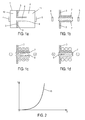
Fig. 1a illustrates a front-view of a self-switching device (SSD), whileFig. 1b, Fig. 1c and Fig. 1d illustrates the modes of operation of the device, - -
Fig. 2 illustrates a current-voltage characteristic of a SSD, - -
Fig. 3 illustrates a front-view of a demodulation device of the invention, - -
Fig. 4 illustrates a detailed view of an antenna of the demodulation device of the invention, - -
Fig. 5 illustrates a side view of a demodulation device of the invention showing the coupling of electromagnetic wave signal, - -
Fig. 6 illustrates the direct demodulation process of a signal by a device of the invention. - With reference to
Fig. 1a , a demodulation device of the invention comprises one or several components usually referred to as "Self-Switching Device", orSSD 1. TheseSSDs 1 are used as demodulators for demodulating the signals, as explained later. - Examples of
SSDs 1 and modes of realization of such components applicable in the context of the invention are described in the documentWO 02/086973 - A
SSD 1 comprises aconductive layer 2. Thisconductive layer 2 is made for instance in an INGaAs/InP substrate containing a conductive layer with mobile electrons, located about 50 nm below the surface. - Other material arrangements may be used for the manufacturing of the SSDs 1:
- high mobility materials such as InAs or InSb may be used in order to reach much higher frequencies;
- even if heterojunctions provide the best performances, a material structure comprising a doped layer on top of an isolating substrate, such as SOI (Silicon On Insulator), may be used for manufacturing the
SSDs 1. In that case, the results in terms of cutoff frequencies may be not the best, but the use of a silicon-based technology may be advantageous for the integration. - Insulating
trenches 3 are made in thatconductive layer 2, using a wet chemical etching technique, or a radiative ion etching (RIE) technique. These insulatingtrenches 3 are for instance about 100 nm deep, so as to be deeper than theconductive layer 2, and to form insulatinglines 3. - The insulating
lines 3 comprise first insulatinglines 8 which separate theconductive layer 2 into afirst area 10 and asecond area 11, except for achannel 6. - The insulating
lines 3 comprise also second insulatinglines 9 which extend from the first insulatinglines 8 into thesecond area 11. These second insulatinglines 9 define thus anelongated channel 6 in theconductive layer 2, which provides an electron flow path for mobile electrons to travel between thefirst area 10 and thesecond areas 11. Thiselongated channel 6 has a typically a length in the order of 1 to 2 micrometers and a width in the order of 50 nm to 100 nm. - The
first area 10 and thesecond area 11 of theconductive layer 2 are connected toelectrical terminals - With reference to
Fig. 1b , when no voltage is applied betweenterminals depletion regions 7 appear in theelongated channel 6 along the insulatingline 9, so that only a narrow area of the flow path is available for electron conduction. Thesedepletion regions 7 are due to surface states and Fermi levels at the etched surface. - With reference to
Fig. 1c , when a positive voltage is applied toterminal 5 and a negative voltage is applied to terminal 4 (or at least when a higher voltage is applied toterminal 5 than to terminal 4), a positive voltage exists on the outer side of insulatinglines 9, which contributes to decrease the size of thedepletion regions 7 by electrostatically lowering the potential in thechannel 6. So the electron conduction and therefore the current flowing in thechannel 6 are larger. - With reference to
Fig. 1d , when now a negative voltage is applied toterminal 5 and a positive voltage is applied to terminal 4 (or at least when a lower voltage is applied toterminal 5 than to terminal 4), a negative voltage exists on the outer side of insulatinglines 9, which contributes to increase the size of thedepletion regions 7 by electrostatically increasing the potential in thechannel 6. This creates a narrower channel or even a pitched-off channel. Thus only little or even no current may flow in thechannel 6. -
Fig. 2 shows a typical current-voltage characteristic 15 ofSSD 1. Current I is plotted in function of voltage V. - It can be seen that the behavior of such component is quite similar to that of a semiconductor diode:
- when a negative voltage is applied on the
terminals SSD 1; - when a positive voltage, higher that a threshold, is applied on these terminals, a current flows through the
SSD 1; - the current varies in a non-linear way for some ranges of positive voltages.
- The current-
voltage characteristics 15 may further be modified by modifying structural parameters of the component such as dimensions and shape of thechannel 6, but also by applying a DC bias voltage on theterminals - For instance:
- when the width of the
channel 6 is increased, the shape of the current-voltage curve becomes more similar to that of a non symmetric resistor (with a saturation for high bias); - reducing the length of the
channel 6 allows increasing the cutoff frequencies; - a geometrical asymmetry, such as for instance a V-shaped geometry in which the
channel 6 has a width that varies from one extremity to the other like a "V", increases the non-linearity of the current-voltage curve, and in particular of the quadratic terms. - So, a
SSD 1 behaves, at least in some extends, like a semiconductor diode even if it works on a completely different principle. - The document
WO 02/086973 - In this kind of applications, a high-frequency voltage is applied on
terminals - The use of diodes for demodulating amplitude-modulated signals is of course known. When a high-frequency carrier signal with a carrier at frequency fc modulated in amplitude with a modulation signal at frequency fm for instance is applied on a
diode 1, the modulation signal at frequency fm may be obtained from the current flowing through the diode. The modulation signal lays actually in the variations, in amplitude, of the positive parts of the carrier signal which are not rejected by the diode. - More precisely, when applying a modulated, high frequency carrier voltage on the diode such as:

- One gets a current which directly contains the modulation information, which may be accessed after proper filtering:

- Of course, the same applies for all modulation frequencies fm in case of broadband modulation signal.
- In practice, direct demodulation is rarely used for high-frequency carrier signals, because notably of the requirements in terms of bandwidth of the components.
- Usually, the modulated carrier signal is transposed in a first step at a lower intermediate frequency by heterodyne mixing with an oscillator. And then the demodulation is done at that lower frequency.
- It is an advantage of the invention to have recognized that
SSDs 1 may have a current-voltage characteristic 15 usable for demodulation applications within a bandwidth extending up to the THz range. In other words, the voltage-current characteristic 15 of theSSD 1 as shown inFig. 2 may be preserved at all useful frequencies within the range. - Simulation results have shown that a stable current-
voltage characteristic 15 may be obtained in a frequency range extending from DC to 450 GHz, or even to 2 THz with some configurations ofSSDs 1, using for instance high mobility materials andchannels 6 with reduced length as previously explained. In other words the current bandwidth may be extended up to 2 THz at least. - This means that SSD can be used for direct demodulation of signals with carrier frequency fc up to 2 THz and modulation frequencies fm of several hundred of GHz. So, huge bandwidth can be achieved for data transmission.
- In addition, these performances may be obtained at room temperature, without cooling.
- With reference to
Fig. 3, Fig. 4 and Fig. 5 , we will now describe ademodulation device 20 usingSSD demodulators 1 for demodulating carrier signals 40 in the THz range and obtaining modulation signals. - The
demodulation device 20 of the invention comprisesseveral SSD demodulators 1. Thesedemodulators 1 are connected through theirterminals patches 30 with a conical shape forming bow-ties antennas 21 (or other types of antennas).Several SSDs 1 are connected in parallel to a pair ofpatches 30 of anantenna 21. TheseSSDs 1 may be done as distinct components, or they may share the sameconductive surface 2 just comprisingseveral channels 6 in parallel. - The
antennas 21 are connected in parallel byconductive links 22, so as to form columns ofantennas 21. Several columns ofantennas 21 are in turn connected in series so as to form an array ofantennas 21 anddemodulators 1. - All the
antennas 21 are oriented along the same direction. - The
antennas 21 and theSSD demodulators 1 are all done on a same surface of acomponent 20 using classical techniques from the semiconductor industry.Antenna patches 30 may for instance be made of pieces or metal vacuum-deposited on the surface holding the already-done SSD. Components bounding may be done by using gold micro-wires. Components bounding may also be done by direct integration of components and/or connection tracks during the fabrication. - So the
demodulation device 20 of the invention is particularly easy to realize. - The planar structure allows also an easy and efficient coupling of high-frequency signals. The carrier signal is brought in the form of a
beam 40 or electromagnetic wave which is focused onto the surface of thedemodulation device 20. Thebeam 40 is focused on the surface holding the antennas 21 (or possibly on the surface opposite), and is coupled with theantennas 21. - The
beam 40 is linearly polarized, with its axis of polarization aligned with the axis of theantennas 21. - The electric field intercepted by each of the
antennas 21 induces a voltage difference on theterminals SSD demodulators 1 which are connected to thepatches 30. As explained before, a resulting current with frequency content at modulation frequencies fm appears on theSSD terminals - As the
SSDs 1 of thedevice 20 are connected in series and in parallel, the resulting currents combine and may be collected at theterminals 23 of the demodulation device, and eventually converted in voltage. - A large part of the surface of the demodulation device is occupied by the
antennas 21, so the structure allows very efficient coupling of the power of the high-frequency carrier signal 40. The modulation signals generated at modulation frequencies by allSSDs 1 are also combined in power to be efficiently collected at the component'sterminals 23. - It is important to notice that this simple and efficient architecture is made possible by the fact that
SSDs 1 have a planar structure requiring only one conductive layer, and that they allow power coupling by the face. This is an important advantage of the device of the invention compared for instance to demodulators based on schottky diodes whose manufacturing requires several layers and in which the coupling of high-frequency power must be done by the side of these layers. -
Fig. 6 illustrates the direct demodulation of a modulatedsignal 50 by aSSD demodulator 1. - As a matter of example, a modulated
signal 50 with a carrier frequency fc in the THz range modulated in amplitude by a harmonic signal at modulation frequency fm is coupled to theSSD demodulator 1. Thissignal 50 may be for instance such as described by Eq. 1. In that case, itsamplitude spectrum 52 comprises a component at carrier frequency fc surrounded by components at frequencies fc + fm et fc - fm, respectively. - As previously explained, a modulation current 51 appears on the terminals of the
SSD demodulator 1, which contains the modulation information. In the example ofFig. 6 , this modulation current may be such as described by Eq. 2. Itsamplitude spectrum 53 comprises components at modulation frequency ±fm which correspond directly to the modulation signal to be extracted, in baseband. So the detection of the modulation current 51, possibly followed by a proper filtering, allows detecting directly the modulation signal carried by the modulatedsignal 50, in baseband. - Of course, the same detection scheme may be applied to any kind of modulation which may be processed in baseband.
- The modulated
signal 50 may be of course a modulatedwave 40 incident on ademodulation device 20 of the invention, comprisingseveral SSDs demodulator 1. In that case theSSD demodulators 1 cooperate to generate a modulation current 51, or more generally speaking amodulation signal 51 with the modulation information. And thismodulation signal 51 may be collected at theterminals 23 of thedemodulation device 20. - While this invention has been described in conjunction with a number of embodiments, it is evident that many alternatives, modifications and variations would be or are apparent to those of ordinary skill in the applicable arts. Accordingly, it is intended to embrace all such alternatives, modifications, equivalents and variations that are within the spirit and scope of this invention.
Claims (16)
- A demodulation device (20) for demodulating an electromagnetic signal derived from a modulation of a carrier signal, comprising at least one demodulator and coupling means (21) for coupling said modulated carrier signal to said demodulator(s) so as to generate a demodulated signal representative of the carrier modulation,
characterized in that said demodulator(s) comprise(s) a self-switching device (SSD) (1) with a conductive substrate (2) and insulating features (3, 8, 9) defining in said conductive substrate an elongated channel (6), said elongated channel (6) providing a charge carrier flow path in said conductive substrate (2) between first and second areas (10, 11), and being dimensioned and arranged such that said charge carrier flow path is limited by depletion regions the size of which is dependent on a voltage difference between said first and second areas (10, 11). - The demodulation device of claim 1, which comprises first coupling means (21) for coupling to the self-switching device (1) a modulated carrier signal in the form of electromagnetic waves, and second coupling means (4, 5, 23) for transmitting a demodulated signal.
- The demodulation device of claim 2, wherein the second coupling means comprise wired connections (4, 5) with the first and second areas (10, 11) of the self switching device(s) (1).
- The demodulation device of claim 2 or 3, wherein the first coupling means comprise at least one planar antenna (21) with a pair of conductive patches (30) connected respectively to the first and second areas (10, 11) of the self switching device(s) (1).
- The demodulation device of claim 4, which comprises biconical or bowtie antenna(s) (21), with the self switching device(s) (1) inserted between the patches (30) of said antenna(s) (21).
- The demodulation device of any of claims 3 to 5, wherein the antenna(s) (21) and the self-switching device(s) (1) are comprised on the same surface.
- The demodulation device of any of claims 3 to 6, which comprises several self-switching devices (1) connected in parallel to the patches (30) of the antenna(s) (21).
- The demodulation device of any of claims 3 to 7, which comprises a plurality of antennas (21) oriented according to a similar direction.
- The demodulation device of any of claims 3 to 8, which comprises a plurality of antennas (21) connected in series and/or in parallel by conductive links (22) between their patches (30), so as to form an array of antennas and demodulators.
- The demodulation device of any of the preceding claims, which is able to process electromagnetic signals (40) with frequencies higher than 0.2 THz.
- A method for demodulating an electromagnetic signal derived from a modulation of a carrier signal, characterized in that it comprises steps of:- coupling a modulated carrier signal to a demodulation device (20) according to any of claims 1 to 10,- collecting a demodulated signal representative of the carrier modulation.
- The method of claim 11, which further comprises a step of irradiating the demodulation device, implementing at least one antenna (21), with a carrier signal in the form of an electromagnetic wave (40).
- The method of claim 12, which comprises a step of irradiating the demodulation device (20) with a modulated carrier signal incident on the surface of the device holding the antenna(s) (21), or opposite to said surface.
- The method of claim 12 or 13, which further comprises steps of irradiating the demodulation device (20) with a linearly polarized carrier signal 40) having an axis of polarization substantially parallel to the orientation of at least some of the antenna(s) (21).
- The method of any of claims 12 to 14, which further comprises steps of irradiating several antennas (21) of an array of antenna and demodulators with a modulated carrier signal (40), and collecting a demodulated signal on said array of antennas and demodulators using wired connections (23).
- A system for demodulating an electromagnetic signal derived from a modulation of a carrier signal, comprising:- a demodulator device (20) according to claim 9 or 10 with an array of antennas and demodulators,- means for directing a carrier signal in the form of an electromagnetic wave (40) on one side of the antenna(s) (21),- wired connection means (23) for collecting a demodulated signal on said array of antennas and demodulators.
Priority Applications (3)
| Application Number | Priority Date | Filing Date | Title |
|---|---|---|---|
| EP12306382.8A EP2731264A1 (en) | 2012-11-08 | 2012-11-08 | Device and method for direct demodulation of signals with carrier frequencies up to the THz range |
| PCT/EP2013/073191 WO2014072356A1 (en) | 2012-11-08 | 2013-11-06 | Device and method for direct demodulation of signals with carrier frequencies up to the thz range |
| EP13798268.2A EP2918011A1 (en) | 2012-11-08 | 2013-11-06 | Device and method for direct demodulation of signals with carrier frequencies up to the thz range |
Applications Claiming Priority (1)
| Application Number | Priority Date | Filing Date | Title |
|---|---|---|---|
| EP12306382.8A EP2731264A1 (en) | 2012-11-08 | 2012-11-08 | Device and method for direct demodulation of signals with carrier frequencies up to the THz range |
Publications (1)
| Publication Number | Publication Date |
|---|---|
| EP2731264A1 true EP2731264A1 (en) | 2014-05-14 |
Family
ID=47189858
Family Applications (2)
| Application Number | Title | Priority Date | Filing Date |
|---|---|---|---|
| EP12306382.8A Withdrawn EP2731264A1 (en) | 2012-11-08 | 2012-11-08 | Device and method for direct demodulation of signals with carrier frequencies up to the THz range |
| EP13798268.2A Withdrawn EP2918011A1 (en) | 2012-11-08 | 2013-11-06 | Device and method for direct demodulation of signals with carrier frequencies up to the thz range |
Family Applications After (1)
| Application Number | Title | Priority Date | Filing Date |
|---|---|---|---|
| EP13798268.2A Withdrawn EP2918011A1 (en) | 2012-11-08 | 2013-11-06 | Device and method for direct demodulation of signals with carrier frequencies up to the thz range |
Country Status (2)
| Country | Link |
|---|---|
| EP (2) | EP2731264A1 (en) |
| WO (1) | WO2014072356A1 (en) |
Citations (5)
| Publication number | Priority date | Publication date | Assignee | Title |
|---|---|---|---|---|
| US2894132A (en) * | 1956-04-23 | 1959-07-07 | Gen Electric | Second detector circuit |
| US4461039A (en) * | 1982-09-20 | 1984-07-17 | Hughes Aircraft Company | Quasi-optical balanced biconical mixer |
| EP0193849A2 (en) * | 1985-03-04 | 1986-09-10 | General Electric Company | Single balanced planar mixer |
| US6265940B1 (en) * | 2000-01-18 | 2001-07-24 | Mitsubishi Denki Kabushiki Kaisha | Detector and transmitter incorporating the detector |
| WO2002086973A2 (en) | 2001-04-20 | 2002-10-31 | Btg International Limited | Nanoelectronic devices and circuits |
Family Cites Families (1)
| Publication number | Priority date | Publication date | Assignee | Title |
|---|---|---|---|---|
| GB9624478D0 (en) * | 1996-11-23 | 1997-01-15 | Matra Bae Dynamics Uk Ltd | Transceivers |
-
2012
- 2012-11-08 EP EP12306382.8A patent/EP2731264A1/en not_active Withdrawn
-
2013
- 2013-11-06 WO PCT/EP2013/073191 patent/WO2014072356A1/en not_active Ceased
- 2013-11-06 EP EP13798268.2A patent/EP2918011A1/en not_active Withdrawn
Patent Citations (6)
| Publication number | Priority date | Publication date | Assignee | Title |
|---|---|---|---|---|
| US2894132A (en) * | 1956-04-23 | 1959-07-07 | Gen Electric | Second detector circuit |
| US4461039A (en) * | 1982-09-20 | 1984-07-17 | Hughes Aircraft Company | Quasi-optical balanced biconical mixer |
| EP0193849A2 (en) * | 1985-03-04 | 1986-09-10 | General Electric Company | Single balanced planar mixer |
| US6265940B1 (en) * | 2000-01-18 | 2001-07-24 | Mitsubishi Denki Kabushiki Kaisha | Detector and transmitter incorporating the detector |
| WO2002086973A2 (en) | 2001-04-20 | 2002-10-31 | Btg International Limited | Nanoelectronic devices and circuits |
| US7224026B2 (en) * | 2001-04-20 | 2007-05-29 | The University Of Manchester | Nanoelectronic devices and circuits |
Non-Patent Citations (1)
| Title |
|---|
| C. BALOCCO ET AL: "Microwave Detection at 110 GHz by Nanowires with Broken Symmetry", NANO LETTERS, vol. 5, no. 7, 1 July 2005 (2005-07-01), pages 1423 - 1427, XP055056485, ISSN: 1530-6984, DOI: 10.1021/nl050779g * |
Also Published As
| Publication number | Publication date |
|---|---|
| EP2918011A1 (en) | 2015-09-16 |
| WO2014072356A1 (en) | 2014-05-15 |
Similar Documents
| Publication | Publication Date | Title |
|---|---|---|
| US7924107B2 (en) | Resonant tunneling structure | |
| Makhlouf et al. | Terahertz sources and receivers: From the past to the future | |
| Arams et al. | Millimeter mixing and detection in bulk InSb | |
| Khalid et al. | $\hbox {In} _ {0.53}\hbox {Ga} _ {0.47}\hbox {As} $ Planar Gunn Diodes Operating at a Fundamental Frequency of 164 GHz | |
| Daher et al. | Room temperature direct and heterodyne detection of 0.28–0.69-THz waves based on GaN 2-DEG unipolar nanochannels | |
| Ito et al. | InP-based planar-antenna-integrated Schottky-barrier diode for millimeter-and sub-millimeter-wave detection | |
| Wang et al. | 15-Gb/s 50-cm wireless link using a high-power compact III–V 84-GHz transmitter | |
| Mélique et al. | Fabrication and performance of InP-based heterostructure barrier varactors in a 250-GHz waveguide tripler | |
| Shiode et al. | Giga-bit wireless communication at 300 GHz using resonant tunneling diode detector | |
| Cornescu et al. | High-efficiency bias stabilization for resonant tunneling diode oscillators | |
| Ito et al. | Broadband heterodyne detection of terahertz‐waves using rectangular‐waveguide‐input Fermi‐level managed barrier diode module | |
| Di Gaspare et al. | Terahertz current oscillations in a gated two-dimensional electron gas with antenna integrated at the channel ends | |
| Schwagmann et al. | Terahertz emission characteristics of ErAs: InGaAs-based photoconductive antennas excited at 1.55 μm | |
| Jayasankar et al. | Development of Supra-THz Schottky diode harmonic mixers | |
| Arzi et al. | Millimeter-wave Signal Generation and Detection via the same Triple Barrier RTD and on-chip Antenna | |
| EP2731263A1 (en) | Device and method for mixing electromagnetic waves with frequencies up to the THz range | |
| EP2731264A1 (en) | Device and method for direct demodulation of signals with carrier frequencies up to the THz range | |
| Suzuki et al. | Terahertz communications using resonant-tunneling-diode oscillators | |
| Maricar et al. | Extraction of second harmonic from an InP based planar Gunn diode using diamond resonator for milli-metric wave frequencies | |
| Novoa-López et al. | Temperature behavior of Gunn oscillations in planar InGaAs diodes | |
| Asada et al. | THz resonant tunneling devices | |
| Hashisaka et al. | Frequency conversion of radio-frequency edge magnetoplasmons using a quantum point contact | |
| Zhong et al. | Numerical and Experimental Investigations of Self-mixing Effect of a Planar Gunn Diode Oscillator | |
| Yang | High mobility hot electron mixers for millimeter waves and submillimeter waves | |
| Maezawa et al. | High-power oscillations in resonant tunneling diode pair oscillator ICs fabricated with metamorphic devices |
Legal Events
| Date | Code | Title | Description |
|---|---|---|---|
| PUAI | Public reference made under article 153(3) epc to a published international application that has entered the european phase |
Free format text: ORIGINAL CODE: 0009012 |
|
| 17P | Request for examination filed |
Effective date: 20121108 |
|
| AK | Designated contracting states |
Kind code of ref document: A1 Designated state(s): AL AT BE BG CH CY CZ DE DK EE ES FI FR GB GR HR HU IE IS IT LI LT LU LV MC MK MT NL NO PL PT RO RS SE SI SK SM TR |
|
| AX | Request for extension of the european patent |
Extension state: BA ME |
|
| STAA | Information on the status of an ep patent application or granted ep patent |
Free format text: STATUS: THE APPLICATION IS DEEMED TO BE WITHDRAWN |
|
| 18D | Application deemed to be withdrawn |
Effective date: 20141115 |