EP2731132A2 - Package structure and method of forming the same - Google Patents
Package structure and method of forming the same Download PDFInfo
- Publication number
- EP2731132A2 EP2731132A2 EP13191021.8A EP13191021A EP2731132A2 EP 2731132 A2 EP2731132 A2 EP 2731132A2 EP 13191021 A EP13191021 A EP 13191021A EP 2731132 A2 EP2731132 A2 EP 2731132A2
- Authority
- EP
- European Patent Office
- Prior art keywords
- semiconductor device
- semiconductor
- electronic device
- package structure
- forming
- Prior art date
- Legal status (The legal status is an assumption and is not a legal conclusion. Google has not performed a legal analysis and makes no representation as to the accuracy of the status listed.)
- Ceased
Links
Images









Classifications
-
- H—ELECTRICITY
- H10—SEMICONDUCTOR DEVICES; ELECTRIC SOLID-STATE DEVICES NOT OTHERWISE PROVIDED FOR
- H10W—GENERIC PACKAGES, INTERCONNECTIONS, CONNECTORS OR OTHER CONSTRUCTIONAL DETAILS OF DEVICES COVERED BY CLASS H10
- H10W20/00—Interconnections in chips, wafers or substrates
- H10W20/01—Manufacture or treatment
- H10W20/021—Manufacture or treatment of interconnections within wafers or substrates
- H10W20/023—Manufacture or treatment of interconnections within wafers or substrates the interconnections being through-semiconductor vias
-
- H—ELECTRICITY
- H10—SEMICONDUCTOR DEVICES; ELECTRIC SOLID-STATE DEVICES NOT OTHERWISE PROVIDED FOR
- H10D—INORGANIC ELECTRIC SEMICONDUCTOR DEVICES
- H10D64/00—Electrodes of devices having potential barriers
- H10D64/20—Electrodes characterised by their shapes, relative sizes or dispositions
- H10D64/23—Electrodes carrying the current to be rectified, amplified, oscillated or switched, e.g. sources, drains, anodes or cathodes
- H10D64/251—Source or drain electrodes for field-effect devices
- H10D64/254—Source or drain electrodes for field-effect devices for lateral devices wherein the source or drain electrodes extend entirely through the semiconductor bodies, e.g. via-holes for back side contacts
-
- H—ELECTRICITY
- H10—SEMICONDUCTOR DEVICES; ELECTRIC SOLID-STATE DEVICES NOT OTHERWISE PROVIDED FOR
- H10P—GENERIC PROCESSES OR APPARATUS FOR THE MANUFACTURE OR TREATMENT OF DEVICES COVERED BY CLASS H10
- H10P14/00—Formation of materials, e.g. in the shape of layers or pillars
- H10P14/40—Formation of materials, e.g. in the shape of layers or pillars of conductive or resistive materials
- H10P14/46—Formation of materials, e.g. in the shape of layers or pillars of conductive or resistive materials using a liquid
- H10P14/47—Electrolytic deposition, i.e. electroplating; Electroless plating
-
- H—ELECTRICITY
- H10—SEMICONDUCTOR DEVICES; ELECTRIC SOLID-STATE DEVICES NOT OTHERWISE PROVIDED FOR
- H10P—GENERIC PROCESSES OR APPARATUS FOR THE MANUFACTURE OR TREATMENT OF DEVICES COVERED BY CLASS H10
- H10P34/00—Irradiation with electromagnetic or particle radiation of wafers, substrates or parts of devices
- H10P34/40—Irradiation with electromagnetic or particle radiation of wafers, substrates or parts of devices with high-energy radiation
- H10P34/42—Irradiation with electromagnetic or particle radiation of wafers, substrates or parts of devices with high-energy radiation with electromagnetic radiation, e.g. laser annealing
-
- H—ELECTRICITY
- H10—SEMICONDUCTOR DEVICES; ELECTRIC SOLID-STATE DEVICES NOT OTHERWISE PROVIDED FOR
- H10W—GENERIC PACKAGES, INTERCONNECTIONS, CONNECTORS OR OTHER CONSTRUCTIONAL DETAILS OF DEVICES COVERED BY CLASS H10
- H10W20/00—Interconnections in chips, wafers or substrates
- H10W20/01—Manufacture or treatment
- H10W20/021—Manufacture or treatment of interconnections within wafers or substrates
- H10W20/023—Manufacture or treatment of interconnections within wafers or substrates the interconnections being through-semiconductor vias
- H10W20/0249—Manufacture or treatment of interconnections within wafers or substrates the interconnections being through-semiconductor vias wherein the through-semiconductor via protrudes from backsides of the chips, wafers or substrates during the manufacture
-
- H—ELECTRICITY
- H10—SEMICONDUCTOR DEVICES; ELECTRIC SOLID-STATE DEVICES NOT OTHERWISE PROVIDED FOR
- H10W—GENERIC PACKAGES, INTERCONNECTIONS, CONNECTORS OR OTHER CONSTRUCTIONAL DETAILS OF DEVICES COVERED BY CLASS H10
- H10W20/00—Interconnections in chips, wafers or substrates
- H10W20/01—Manufacture or treatment
- H10W20/021—Manufacture or treatment of interconnections within wafers or substrates
- H10W20/023—Manufacture or treatment of interconnections within wafers or substrates the interconnections being through-semiconductor vias
- H10W20/0261—Manufacture or treatment of interconnections within wafers or substrates the interconnections being through-semiconductor vias characterised by the filling method or the material of the conductive fill
-
- H—ELECTRICITY
- H10—SEMICONDUCTOR DEVICES; ELECTRIC SOLID-STATE DEVICES NOT OTHERWISE PROVIDED FOR
- H10W—GENERIC PACKAGES, INTERCONNECTIONS, CONNECTORS OR OTHER CONSTRUCTIONAL DETAILS OF DEVICES COVERED BY CLASS H10
- H10W20/00—Interconnections in chips, wafers or substrates
- H10W20/01—Manufacture or treatment
- H10W20/031—Manufacture or treatment of conductive parts of the interconnections
- H10W20/056—Manufacture or treatment of conductive parts of the interconnections by filling conductive material into holes, grooves or trenches
- H10W20/057—Manufacture or treatment of conductive parts of the interconnections by filling conductive material into holes, grooves or trenches by selectively depositing, e.g. by using selective CVD or plating
-
- H—ELECTRICITY
- H10—SEMICONDUCTOR DEVICES; ELECTRIC SOLID-STATE DEVICES NOT OTHERWISE PROVIDED FOR
- H10W—GENERIC PACKAGES, INTERCONNECTIONS, CONNECTORS OR OTHER CONSTRUCTIONAL DETAILS OF DEVICES COVERED BY CLASS H10
- H10W20/00—Interconnections in chips, wafers or substrates
- H10W20/01—Manufacture or treatment
- H10W20/031—Manufacture or treatment of conductive parts of the interconnections
- H10W20/0698—Local interconnections
-
- H—ELECTRICITY
- H10—SEMICONDUCTOR DEVICES; ELECTRIC SOLID-STATE DEVICES NOT OTHERWISE PROVIDED FOR
- H10W—GENERIC PACKAGES, INTERCONNECTIONS, CONNECTORS OR OTHER CONSTRUCTIONAL DETAILS OF DEVICES COVERED BY CLASS H10
- H10W20/00—Interconnections in chips, wafers or substrates
- H10W20/01—Manufacture or treatment
- H10W20/071—Manufacture or treatment of dielectric parts thereof
- H10W20/074—Manufacture or treatment of dielectric parts thereof of dielectric parts comprising thin functional dielectric layers, e.g. dielectric etch-stop, barrier, capping or liner layers
- H10W20/077—Manufacture or treatment of dielectric parts thereof of dielectric parts comprising thin functional dielectric layers, e.g. dielectric etch-stop, barrier, capping or liner layers on sidewalls or on top surfaces of conductors
-
- H—ELECTRICITY
- H10—SEMICONDUCTOR DEVICES; ELECTRIC SOLID-STATE DEVICES NOT OTHERWISE PROVIDED FOR
- H10W—GENERIC PACKAGES, INTERCONNECTIONS, CONNECTORS OR OTHER CONSTRUCTIONAL DETAILS OF DEVICES COVERED BY CLASS H10
- H10W20/00—Interconnections in chips, wafers or substrates
- H10W20/20—Interconnections within wafers or substrates, e.g. through-silicon vias [TSV]
-
- H—ELECTRICITY
- H10—SEMICONDUCTOR DEVICES; ELECTRIC SOLID-STATE DEVICES NOT OTHERWISE PROVIDED FOR
- H10W—GENERIC PACKAGES, INTERCONNECTIONS, CONNECTORS OR OTHER CONSTRUCTIONAL DETAILS OF DEVICES COVERED BY CLASS H10
- H10W70/00—Package substrates; Interposers; Redistribution layers [RDL]
- H10W70/40—Leadframes
- H10W70/481—Leadframes for devices being provided for in groups H10D8/00 - H10D48/00
-
- H—ELECTRICITY
- H10—SEMICONDUCTOR DEVICES; ELECTRIC SOLID-STATE DEVICES NOT OTHERWISE PROVIDED FOR
- H10W—GENERIC PACKAGES, INTERCONNECTIONS, CONNECTORS OR OTHER CONSTRUCTIONAL DETAILS OF DEVICES COVERED BY CLASS H10
- H10W90/00—Package configurations
-
- H—ELECTRICITY
- H10—SEMICONDUCTOR DEVICES; ELECTRIC SOLID-STATE DEVICES NOT OTHERWISE PROVIDED FOR
- H10W—GENERIC PACKAGES, INTERCONNECTIONS, CONNECTORS OR OTHER CONSTRUCTIONAL DETAILS OF DEVICES COVERED BY CLASS H10
- H10W90/00—Package configurations
- H10W90/811—Multiple chips on leadframes
-
- H—ELECTRICITY
- H10—SEMICONDUCTOR DEVICES; ELECTRIC SOLID-STATE DEVICES NOT OTHERWISE PROVIDED FOR
- H10W—GENERIC PACKAGES, INTERCONNECTIONS, CONNECTORS OR OTHER CONSTRUCTIONAL DETAILS OF DEVICES COVERED BY CLASS H10
- H10W99/00—Subject matter not provided for in other groups of this subclass
-
- H—ELECTRICITY
- H10—SEMICONDUCTOR DEVICES; ELECTRIC SOLID-STATE DEVICES NOT OTHERWISE PROVIDED FOR
- H10D—INORGANIC ELECTRIC SEMICONDUCTOR DEVICES
- H10D30/00—Field-effect transistors [FET]
- H10D30/40—FETs having zero-dimensional [0D], one-dimensional [1D] or two-dimensional [2D] charge carrier gas channels
- H10D30/47—FETs having zero-dimensional [0D], one-dimensional [1D] or two-dimensional [2D] charge carrier gas channels having two-dimensional [2D] charge carrier gas channels, e.g. nanoribbon FETs or high electron mobility transistors [HEMT]
- H10D30/471—High electron mobility transistors [HEMT] or high hole mobility transistors [HHMT]
- H10D30/475—High electron mobility transistors [HEMT] or high hole mobility transistors [HHMT] having wider bandgap layer formed on top of lower bandgap active layer, e.g. undoped barrier HEMTs such as i-AlGaN/GaN HEMTs
-
- H—ELECTRICITY
- H10—SEMICONDUCTOR DEVICES; ELECTRIC SOLID-STATE DEVICES NOT OTHERWISE PROVIDED FOR
- H10D—INORGANIC ELECTRIC SEMICONDUCTOR DEVICES
- H10D62/00—Semiconductor bodies, or regions thereof, of devices having potential barriers
- H10D62/80—Semiconductor bodies, or regions thereof, of devices having potential barriers characterised by the materials
- H10D62/85—Semiconductor bodies, or regions thereof, of devices having potential barriers characterised by the materials being Group III-V materials, e.g. GaAs
- H10D62/8503—Nitride Group III-V materials, e.g. AlN or GaN
-
- H—ELECTRICITY
- H10—SEMICONDUCTOR DEVICES; ELECTRIC SOLID-STATE DEVICES NOT OTHERWISE PROVIDED FOR
- H10W—GENERIC PACKAGES, INTERCONNECTIONS, CONNECTORS OR OTHER CONSTRUCTIONAL DETAILS OF DEVICES COVERED BY CLASS H10
- H10W70/00—Package substrates; Interposers; Redistribution layers [RDL]
- H10W70/60—Insulating or insulated package substrates; Interposers; Redistribution layers
- H10W70/62—Insulating or insulated package substrates; Interposers; Redistribution layers characterised by their interconnections
- H10W70/65—Shapes or dispositions of interconnections
-
- H—ELECTRICITY
- H10—SEMICONDUCTOR DEVICES; ELECTRIC SOLID-STATE DEVICES NOT OTHERWISE PROVIDED FOR
- H10W—GENERIC PACKAGES, INTERCONNECTIONS, CONNECTORS OR OTHER CONSTRUCTIONAL DETAILS OF DEVICES COVERED BY CLASS H10
- H10W72/00—Interconnections or connectors in packages
- H10W72/01—Manufacture or treatment
- H10W72/019—Manufacture or treatment of bond pads
- H10W72/01921—Manufacture or treatment of bond pads using local deposition
- H10W72/01923—Manufacture or treatment of bond pads using local deposition in liquid form, e.g. by dispensing droplets or by screen printing
-
- H—ELECTRICITY
- H10—SEMICONDUCTOR DEVICES; ELECTRIC SOLID-STATE DEVICES NOT OTHERWISE PROVIDED FOR
- H10W—GENERIC PACKAGES, INTERCONNECTIONS, CONNECTORS OR OTHER CONSTRUCTIONAL DETAILS OF DEVICES COVERED BY CLASS H10
- H10W72/00—Interconnections or connectors in packages
- H10W72/071—Connecting or disconnecting
- H10W72/072—Connecting or disconnecting of bump connectors
-
- H—ELECTRICITY
- H10—SEMICONDUCTOR DEVICES; ELECTRIC SOLID-STATE DEVICES NOT OTHERWISE PROVIDED FOR
- H10W—GENERIC PACKAGES, INTERCONNECTIONS, CONNECTORS OR OTHER CONSTRUCTIONAL DETAILS OF DEVICES COVERED BY CLASS H10
- H10W72/00—Interconnections or connectors in packages
- H10W72/071—Connecting or disconnecting
- H10W72/072—Connecting or disconnecting of bump connectors
- H10W72/07231—Techniques
- H10W72/07236—Soldering or alloying
-
- H—ELECTRICITY
- H10—SEMICONDUCTOR DEVICES; ELECTRIC SOLID-STATE DEVICES NOT OTHERWISE PROVIDED FOR
- H10W—GENERIC PACKAGES, INTERCONNECTIONS, CONNECTORS OR OTHER CONSTRUCTIONAL DETAILS OF DEVICES COVERED BY CLASS H10
- H10W72/00—Interconnections or connectors in packages
- H10W72/071—Connecting or disconnecting
- H10W72/072—Connecting or disconnecting of bump connectors
- H10W72/07251—Connecting or disconnecting of bump connectors characterised by changes in properties of the bump connectors during connecting
- H10W72/07254—Connecting or disconnecting of bump connectors characterised by changes in properties of the bump connectors during connecting changes in dispositions
-
- H—ELECTRICITY
- H10—SEMICONDUCTOR DEVICES; ELECTRIC SOLID-STATE DEVICES NOT OTHERWISE PROVIDED FOR
- H10W—GENERIC PACKAGES, INTERCONNECTIONS, CONNECTORS OR OTHER CONSTRUCTIONAL DETAILS OF DEVICES COVERED BY CLASS H10
- H10W72/00—Interconnections or connectors in packages
- H10W72/20—Bump connectors, e.g. solder bumps or copper pillars; Dummy bumps; Thermal bumps
- H10W72/241—Dispositions, e.g. layouts
-
- H—ELECTRICITY
- H10—SEMICONDUCTOR DEVICES; ELECTRIC SOLID-STATE DEVICES NOT OTHERWISE PROVIDED FOR
- H10W—GENERIC PACKAGES, INTERCONNECTIONS, CONNECTORS OR OTHER CONSTRUCTIONAL DETAILS OF DEVICES COVERED BY CLASS H10
- H10W72/00—Interconnections or connectors in packages
- H10W72/20—Bump connectors, e.g. solder bumps or copper pillars; Dummy bumps; Thermal bumps
- H10W72/241—Dispositions, e.g. layouts
- H10W72/244—Dispositions, e.g. layouts relative to underlying supporting features, e.g. bond pads, RDLs or vias
-
- H—ELECTRICITY
- H10—SEMICONDUCTOR DEVICES; ELECTRIC SOLID-STATE DEVICES NOT OTHERWISE PROVIDED FOR
- H10W—GENERIC PACKAGES, INTERCONNECTIONS, CONNECTORS OR OTHER CONSTRUCTIONAL DETAILS OF DEVICES COVERED BY CLASS H10
- H10W72/00—Interconnections or connectors in packages
- H10W72/20—Bump connectors, e.g. solder bumps or copper pillars; Dummy bumps; Thermal bumps
- H10W72/241—Dispositions, e.g. layouts
- H10W72/247—Dispositions of multiple bumps
-
- H—ELECTRICITY
- H10—SEMICONDUCTOR DEVICES; ELECTRIC SOLID-STATE DEVICES NOT OTHERWISE PROVIDED FOR
- H10W—GENERIC PACKAGES, INTERCONNECTIONS, CONNECTORS OR OTHER CONSTRUCTIONAL DETAILS OF DEVICES COVERED BY CLASS H10
- H10W72/00—Interconnections or connectors in packages
- H10W72/20—Bump connectors, e.g. solder bumps or copper pillars; Dummy bumps; Thermal bumps
- H10W72/251—Materials
- H10W72/252—Materials comprising solid metals or solid metalloids, e.g. PbSn, Ag or Cu
-
- H—ELECTRICITY
- H10—SEMICONDUCTOR DEVICES; ELECTRIC SOLID-STATE DEVICES NOT OTHERWISE PROVIDED FOR
- H10W—GENERIC PACKAGES, INTERCONNECTIONS, CONNECTORS OR OTHER CONSTRUCTIONAL DETAILS OF DEVICES COVERED BY CLASS H10
- H10W72/00—Interconnections or connectors in packages
- H10W72/20—Bump connectors, e.g. solder bumps or copper pillars; Dummy bumps; Thermal bumps
- H10W72/29—Bond pads specially adapted therefor
-
- H—ELECTRICITY
- H10—SEMICONDUCTOR DEVICES; ELECTRIC SOLID-STATE DEVICES NOT OTHERWISE PROVIDED FOR
- H10W—GENERIC PACKAGES, INTERCONNECTIONS, CONNECTORS OR OTHER CONSTRUCTIONAL DETAILS OF DEVICES COVERED BY CLASS H10
- H10W72/00—Interconnections or connectors in packages
- H10W72/851—Dispositions of multiple connectors or interconnections
- H10W72/853—On the same surface
- H10W72/871—Bond wires and strap connectors
-
- H—ELECTRICITY
- H10—SEMICONDUCTOR DEVICES; ELECTRIC SOLID-STATE DEVICES NOT OTHERWISE PROVIDED FOR
- H10W—GENERIC PACKAGES, INTERCONNECTIONS, CONNECTORS OR OTHER CONSTRUCTIONAL DETAILS OF DEVICES COVERED BY CLASS H10
- H10W72/00—Interconnections or connectors in packages
- H10W72/851—Dispositions of multiple connectors or interconnections
- H10W72/874—On different surfaces
- H10W72/879—Bump connectors and bond wires
-
- H—ELECTRICITY
- H10—SEMICONDUCTOR DEVICES; ELECTRIC SOLID-STATE DEVICES NOT OTHERWISE PROVIDED FOR
- H10W—GENERIC PACKAGES, INTERCONNECTIONS, CONNECTORS OR OTHER CONSTRUCTIONAL DETAILS OF DEVICES COVERED BY CLASS H10
- H10W72/00—Interconnections or connectors in packages
- H10W72/851—Dispositions of multiple connectors or interconnections
- H10W72/874—On different surfaces
- H10W72/881—Bump connectors and strap connectors
-
- H—ELECTRICITY
- H10—SEMICONDUCTOR DEVICES; ELECTRIC SOLID-STATE DEVICES NOT OTHERWISE PROVIDED FOR
- H10W—GENERIC PACKAGES, INTERCONNECTIONS, CONNECTORS OR OTHER CONSTRUCTIONAL DETAILS OF DEVICES COVERED BY CLASS H10
- H10W72/00—Interconnections or connectors in packages
- H10W72/90—Bond pads, in general
- H10W72/921—Structures or relative sizes of bond pads
- H10W72/922—Bond pads being integral with underlying chip-level interconnections
-
- H—ELECTRICITY
- H10—SEMICONDUCTOR DEVICES; ELECTRIC SOLID-STATE DEVICES NOT OTHERWISE PROVIDED FOR
- H10W—GENERIC PACKAGES, INTERCONNECTIONS, CONNECTORS OR OTHER CONSTRUCTIONAL DETAILS OF DEVICES COVERED BY CLASS H10
- H10W72/00—Interconnections or connectors in packages
- H10W72/90—Bond pads, in general
- H10W72/921—Structures or relative sizes of bond pads
- H10W72/922—Bond pads being integral with underlying chip-level interconnections
- H10W72/9226—Bond pads being integral with underlying chip-level interconnections with via interconnections
-
- H—ELECTRICITY
- H10—SEMICONDUCTOR DEVICES; ELECTRIC SOLID-STATE DEVICES NOT OTHERWISE PROVIDED FOR
- H10W—GENERIC PACKAGES, INTERCONNECTIONS, CONNECTORS OR OTHER CONSTRUCTIONAL DETAILS OF DEVICES COVERED BY CLASS H10
- H10W72/00—Interconnections or connectors in packages
- H10W72/90—Bond pads, in general
- H10W72/921—Structures or relative sizes of bond pads
- H10W72/923—Bond pads having multiple stacked layers
-
- H—ELECTRICITY
- H10—SEMICONDUCTOR DEVICES; ELECTRIC SOLID-STATE DEVICES NOT OTHERWISE PROVIDED FOR
- H10W—GENERIC PACKAGES, INTERCONNECTIONS, CONNECTORS OR OTHER CONSTRUCTIONAL DETAILS OF DEVICES COVERED BY CLASS H10
- H10W72/00—Interconnections or connectors in packages
- H10W72/90—Bond pads, in general
- H10W72/931—Shapes of bond pads
- H10W72/934—Cross-sectional shape, i.e. in side view
-
- H—ELECTRICITY
- H10—SEMICONDUCTOR DEVICES; ELECTRIC SOLID-STATE DEVICES NOT OTHERWISE PROVIDED FOR
- H10W—GENERIC PACKAGES, INTERCONNECTIONS, CONNECTORS OR OTHER CONSTRUCTIONAL DETAILS OF DEVICES COVERED BY CLASS H10
- H10W72/00—Interconnections or connectors in packages
- H10W72/90—Bond pads, in general
- H10W72/941—Dispositions of bond pads
- H10W72/942—Dispositions of bond pads relative to underlying supporting features, e.g. bond pads, RDLs or vias
-
- H—ELECTRICITY
- H10—SEMICONDUCTOR DEVICES; ELECTRIC SOLID-STATE DEVICES NOT OTHERWISE PROVIDED FOR
- H10W—GENERIC PACKAGES, INTERCONNECTIONS, CONNECTORS OR OTHER CONSTRUCTIONAL DETAILS OF DEVICES COVERED BY CLASS H10
- H10W72/00—Interconnections or connectors in packages
- H10W72/90—Bond pads, in general
- H10W72/941—Dispositions of bond pads
- H10W72/944—Dispositions of multiple bond pads
-
- H—ELECTRICITY
- H10—SEMICONDUCTOR DEVICES; ELECTRIC SOLID-STATE DEVICES NOT OTHERWISE PROVIDED FOR
- H10W—GENERIC PACKAGES, INTERCONNECTIONS, CONNECTORS OR OTHER CONSTRUCTIONAL DETAILS OF DEVICES COVERED BY CLASS H10
- H10W72/00—Interconnections or connectors in packages
- H10W72/90—Bond pads, in general
- H10W72/951—Materials of bond pads
- H10W72/952—Materials of bond pads comprising metals or metalloids, e.g. PbSn, Ag or Cu
-
- H—ELECTRICITY
- H10—SEMICONDUCTOR DEVICES; ELECTRIC SOLID-STATE DEVICES NOT OTHERWISE PROVIDED FOR
- H10W—GENERIC PACKAGES, INTERCONNECTIONS, CONNECTORS OR OTHER CONSTRUCTIONAL DETAILS OF DEVICES COVERED BY CLASS H10
- H10W90/00—Package configurations
- H10W90/701—Package configurations characterised by the relative positions of pads or connectors relative to package parts
- H10W90/721—Package configurations characterised by the relative positions of pads or connectors relative to package parts of bump connectors
- H10W90/722—Package configurations characterised by the relative positions of pads or connectors relative to package parts of bump connectors between stacked chips
-
- H—ELECTRICITY
- H10—SEMICONDUCTOR DEVICES; ELECTRIC SOLID-STATE DEVICES NOT OTHERWISE PROVIDED FOR
- H10W—GENERIC PACKAGES, INTERCONNECTIONS, CONNECTORS OR OTHER CONSTRUCTIONAL DETAILS OF DEVICES COVERED BY CLASS H10
- H10W90/00—Package configurations
- H10W90/701—Package configurations characterised by the relative positions of pads or connectors relative to package parts
- H10W90/721—Package configurations characterised by the relative positions of pads or connectors relative to package parts of bump connectors
- H10W90/724—Package configurations characterised by the relative positions of pads or connectors relative to package parts of bump connectors between a chip and a stacked insulating package substrate, interposer or RDL
Definitions
- This invention relates generally to semiconductor devices, and specifically, to package structures and methods for fabricating the same.
- Semiconductor components include external contacts that allow electrical connections to be made from the outside to the integrated circuits contained in the semiconductor components.
- a semiconductor die for example, includes patterns of bond pads formed on the face of the die.
- Semiconductor packages such as chip scale packages, also include external contacts.
- a component typically includes only one set of external contacts on either the face side (circuit side) or the back side of the component. However, it is sometimes necessary for a component to have external contacts on both sides.
- a through-silicon via also known as a through-substrate via
- a through-silicon via is a conductive feature formed in a semiconductor substrate (wafer or die) to electrically connect external contacts from both sides.
- the TSV feature vertically passes through the semiconductor substrate, providing for stacked wafer/die packaging methods and allowing for electrical connection between circuits within separate wafers or chips.
- a hole is etched into the semiconductor substrate, and sometimes through the interconnect structure as well. The hole may then be lined with various isolating layers and/or various metal layers. The hole is then filled with a conductive material, typically copper (Cu), which becomes the major part of a TSV.
- Cu copper
- an electrode electroplating method is used for the conductive filling materials to be disposed in the hole of the through silicon via (TSV), wherein a seeding layer is formed by a vacuum technique, such as plasma vapor deposition, prior to formation of the conductive filling material.
- TSV through silicon via
- the vacuum technique requires high-priced equipment, which increases device costs.
- the invention provides a package structure including: a first semiconductor device including a first semiconductor substrate and a first electronic device, the first semiconductor device having a first side and a second side opposite to the first side, wherein at least part of the first electronic device being adjacent to the first side, and wherein the first semiconductor device has a via-hole formed through the first semiconductor device, wherein the via-hole has a first opening adjacent to the first side; an interconnection structure disposed in the first semiconductor device, wherein the interconnection structure comprises: a via structure disposed in the via-hole without exceeding the first opening; a first pad disposed on the first side of the first semiconductor device and covering the via-hole, wherein the first pad is adjoined to the via structure and is electrically connected to the first electronic device; and a second semiconductor device vertically integrated with the first semiconductor device, wherein the second semiconductor device comprises a second electronic device electrically connected with the first electronic device.
- the invention provides a method of forming a package structure including: providing a first semiconductor device having a first side and a second side opposite to the first side; forming a via-hole through the first semiconductor device, wherein the via-hole has a first opening neighboring the first side and a second opening neighboring the second side; forming a first pad covering the first opening; forming a via structure in the via-hole subsequent to forming the first pad, wherein the via structure comprises a conductive material and is adjoined to the first pad; and substantially vertically integrating the first semiconductor device with a second semiconductor device.
- a method for forming a first semiconductor device 100 with an interconnection structure of an embodiment of the invention is illustrated in accordance with FIG. 1A to FIG. 1F .
- a first semiconductor device 100 is provided.
- the first semiconductor device 100 includes a first side 106 and a second side 108 opposite to the first side 106.
- the first semiconductor device 100 includes a substrate 102.
- the substrate 102 can be any suitable semiconductor material.
- the substrate 102 can be Si, SiC, Ge, SiGe, GaAs, InAs, InP or GaN.
- a buffer layer 104 is formed on the substrate 102.
- the buffer layer 104 can be a nitride based material to provide good adhesion for the layers thereon and also solve issues of lattice mismatch, but the invention is not limited thereto.
- the buffer layer 104 can be formed of any suitable material.
- the buffer layer 104 can be aluminum nitride.
- a channel layer 110 and a barrier layer 112 are formed on the buffer layer 104.
- the channel layer 110 can be GaN and the barrier layer 112 can be AlGaN.
- a first metal layer (not shown) is formed on the channel layer 110 and is then patterned by lithography and etching to form a source electrode 118 and a drain electrode 120.
- the first metal layer is a stack of Ti, Al, Ni and/or Au layers. Furthermore, a rapid thermal annealing (RTA) process can be performed to the first metal layer.
- RTA rapid thermal annealing
- a second metal layer (not shown) is deposited on the channel layer 110 and then patterned by lithography and etching to form a gate electrode 116.
- a passivation layer 122 such as a silicon nitride or silicon oxide layer, is formed to protect the device thereunder.
- the channel layer 110, the barrier layer 112, the gate electrode 116, the source electrode 118, and the drain electrode 120 constitute an electronic device 114 adjacent to the first side 106 of the first semiconductor device 100.
- the electronic device 114 is disposed at the first side 106 of the first semiconductor device 100, but the invention is not limited thereto.
- the electronic device 114 can be disposed at the second side 108 of the first semiconductor device 100.
- the electronic device 114 is a nitride-based semiconductor device.
- the invention is not limited to a nitride-based semiconductor device.
- the invention can be applied to any semiconductor device, such as a silicon based device, III-V group device and/or SOI device.
- a photosensitive layer 124 is formed over the substrate 102 and the electronic device 114. Thereafter, referring to FIG. 1C , the photosensitive layer 124 is patterned by a lithography process and the substrate 102 is further etched using the patterned photosensitive layer 124 as a mask to form a via-hole 126 extending through the substrate 102.
- the via-hole 126 can be formed with drilling using a laser beam.
- the photoresist layer 124 is then removed.
- an insulating layer 128 is optionaly formed on the sidewall of the via-hole 126 for protection.
- the insulating layer 128 is silicon oxide and can be formed by thermal oxidation or liquid phase deposition (LPD).
- the via-hole 126 has a first opening 111 neighboring the first side 106 and a second opening 113 neighboring the second side 108.
- a first pad 130 is formed on the first side 106 of the first semiconductor device 100 and covers the first opening 111 of the via-hole 126.
- the first pad 130 can electrically connect to the electrical device 114 and a second pad 134 formed in subsequent steps, and can comprise a protrusion portion extending into the via-hole 126.
- the first pad 130 can comprise silver paste and can be formed by screen printing.
- an electroplating process is performed using the first pad 130 as a seed layer to deposit a via structure 132 which fills the via-hole 126.
- the via structure 132 and the first pad 130 comprises the same material.
- the via structure 132 and the first pad 130 comprises different materials.
- the via structure 132 can comprise copper.
- the via structure 132 since the via structure 132 is formed sequentially after forming the first pad 130, the via structure 132 does not exceed the first opening 111 of the via-hole 126 neighboring the first side 106 of the first semiconductor device, but can exceed the second opening 113 of the via-hole 126 neighboring the second side 108 of the first semiconductor device.
- a second pad 134 is formed on the second side 108 of the first semiconductor device 100.
- the second pad 134 can comprise silver paste and can be formed by screen printing.
- the first semiconductor device 100 includes the semiconductor substrate 102 and an electronic device 114.
- the first semiconductor device 100 has the first side 106 and the second side 108 opposite to the first side 106. At least part of the electronic device 114 is adjacent to the first side 106.
- the first semiconductor device 100 has the via-hole 126 formed through the first semiconductor device 100, wherein the via-hole 126 has the first opening 111 adjacent to the first side 106.
- An interconnection structure C is disposed in the first semiconductor device 100, wherein the interconnection structure C includes the via structure 132 and the first pad 130.
- the via structure 132 is disposed in the via-hole 126 without exceeding the first opening 111.
- the first pad 130 is disposed on the first side 106 of the first semiconductor device 100 and covers the via-hole 126, wherein the first pad 130 is adjoined to the via structure 132 and is electrically connected to the electronic device 114.
- the electrical device 114 is a high electron mobility transistor (HEMT) and the substrate 102 comprises a semiconductor substrate.
- the source electrode 118 is electrically connected to the semiconductor substrate through the via structure 132.
- a method for forming a first semiconductor device of another embodiment of the invention is illustrated in accordance with FIG. 2 .
- the embodiment of the method for forming the first semiconductor device of FIG. 2 is similar to the method of FIGS. 1E ⁇ 1F and for simplicity its detailed descriptions of similar steps are omitted.
- the method for forming the first semiconductor device of FIG. 2 is different from the method for forming the first semiconductor device of FIGS. 1E ⁇ 1F in that the first pad 202 and the via structure 204 are formed by a single step.
- the screen print for forming the first pad 202 can also fill the through hole 126, so that formation of the first pad 202 and the via structure 204 can be performed by a single screen printing step.
- a method for forming a first semiconductor device of yet another embodiment of the invention is illustrated in accordance with FIG. 3A to FIG. 3F .
- the method of the embodiment illustrated in FIG. 3A to FIG. 3F differs from the embodiment illustrated in FIG. 1A to FIG. 1F by the forming of the pad on the second side of the substrate opposite to the first side with the electronic device prior to forming the via structure.
- a semiconductor device 300 is provided.
- the semiconductor device 300 has a first side 306 and a second side 308.
- the semiconductor device 300 has a substrate 302.
- the substrate 302 can be any suitable semiconductor material.
- the substrate 302 can be Si, SiC, Ge, SiGe, GaAs, InAs, InP or GaN.
- a buffer layer 304 is formed on the substrate 302.
- the buffer layer 304 can be aluminum nitride.
- a channel layer 310 and a barrier layer 312 are formed on the buffer layer 304.
- the channel layer 310 can be GaN and the barrier layer 312 can be AlGaN.
- a first metal layer (not shown) is formed on the channel layer 310 and is then patterned by lithography and etching to form a source electrode 318 and a drain electrode 320.
- the first metal layer is a stack of Ti, Al, Ni or Au layers.
- RTA rapid thermal annealing
- a second metal layer (not shown) is deposited and then patterned by lithography and etching to form a gate electrode 316.
- the channel layer 310, the barrier layer 312, the gate electrode 316, the source electrode 318, and the drain electrode 320 constitute an electronic device 314 which is adjacent to the first side 306 of the substrate 302.
- the electronic device 314 is a nitride-based semiconductor device.
- the invention is not limited to being applied to a nitride-based semiconductor device.
- the invention can be applied to any semiconductor device, such as a silicon based device, III-V group device and/or SOI device.
- a photosensitive layer 324 is formed over the substrate 302 to protect the electronic device 314.
- the photosensitive layer 324 is patterned by a lithography process and the substrate 302 is further etched using the patterned photosensitive layer 324 as a mask to form a via-hole 326 extending through the substrate 302 is formed.
- the via-hole 326 can be formed by a laser beam.
- the photoresist layer 324 is then removed.
- an insulating layer 328 is optionally formed on the sidewall of the via-hole 326 for protection.
- the insulating layer 328 is silicon oxide and can be formed by thermal oxidation or liquid phase deposition (LPD).
- a first pad 330 is formed on the second side 308 of the substrate 302 and covers a second opening 311 of the via-hole 326.
- the first pad 330 can comprise silver paste and can be formed by screen printing.
- an electroplating process is performed using the first pad 330 as a seed layer to form a via structure 332 which fills the via-hole 326.
- the via structure 332 and the first pad 330 comprise the same material.
- the via structure 332 and the first pad 330 comprise different materials.
- the via structure 332 can comprise copper. As shown in FIG.
- a second pad 334 such as silver, is formed on the first side 306 of the substrate 302.
- the semiconductor device 300 includes the semiconductor substrate 302 and the electronic device 314.
- the semiconductor device 300 has the first side 306 and the second side 308 opposite to the first side 306. At least part of the electronic device 314 is adjacent to the first side 306.
- the semiconductor device 300 has the via-hole 326 formed through the semiconductor device 300, wherein the via-hole 326 has the first opening 313 adjacent to the first side 306 and the second opening 311 adjacent to the second side 308.
- An interconnection structure C1 is disposed in the semiconductor device 300, wherein the interconnection structure C1 includes the via structure 332 and the first pad 330.
- the via structure 332 is disposed in the via-hole 326 without exceeding the first opening 311.
- the first pad 330 is disposed on the second side 308 of the semiconductor device 300 and covers the via-hole 326, wherein the first pad 330 is adjoined to the via structure 332 and is electrically connected to the electronic device 314.
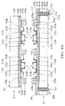
- Figs. 4A-4B show intermediate stages of cross sections of a method for forming a package structure of an embodiment of the invention.
- a first semiconductor device K1 and a second semiconductor device K2 are provided.
- the first semiconductor device K1 has a first side 106 and a second side 108 opposite to the first side 106.
- the first semiconductor device K1 has a first semiconductor substrate 102a and a plurality of first electronic devices 114a.
- the first semiconductor substrate 102a is the same as the substrate 102 shown in Fig. 1A .
- the first semiconductor substrate 102a may be a die or a wafer.
- the first electronic devices 114a are disposed on the first side 106.
- a plurality of via-holes 126a are formed through the first semiconductor substrate 102a, wherein each of the via-holes 126a has a first opening 111 adjacent to the first side 106 and a second opening 113 adjacent to the second side 108.
- the first electronic devices 114a may be a transistor and includes the channel layer 110a, the barrier layer 112a, the gate electrode 116a, the source electrode 118a, and the drain electrode 120a.
- Interconnection structures 410 are disposed in the first semiconductor substrate 102a, wherein each of the interconnection structures 410 includes a via structure 132a and a first pad 130.
- the via structure 132a is disposed in the via-hole 126a without exceeding the first opening 111
- the first pad 130a is disposed on the first side 106 of the first semiconductor substrate 102a and covers the via-hole 126a, wherein the first pad 130a is adjoined to the via structure 132a and is electrically connected to the first electronic device 114a.
- a portion of the first pad 130a extends into the via-hole 126a.
- the interconnection structure 410 may further include a second pad 134a covering the second opening 113 and be adjoined with the via structure 132a.
- a redistribution layer 420a is formed on the first side 106 to electrically connect the first pad 130a and the first electronic device 114a.
- a plurality of bumps 430a may be formed on the first side 106 and may be electrically connected to the first pad 130a and the first electronic device 114a through the redistribution layer 420a.
- the bumps 430a include copper, solder or other suitable materials.
- An under bump metallurgy (UBM) layer 432a may be formed between the bumps 430a and the channel layer 110a.
- a passivation layer 122a such as silicon nitride and silicon oxide, is formed to protect the first electronic device 114a thereunder.
- the second semiconductor device K2 has a third side S3 and a fourth side S4 opposite to the third side S3, and the second semiconductor device K2 includes a second semiconductor substrate 102b (which is the same as the substrate 102 shown in Fig. 1A ) and second electronic devices 114b disposed on the second semiconductor substrate 102b.
- the second electronic devices 114b are adjacent to the third side S3.
- the second semiconductor substrate 102b may be a die.
- the second electronic devices 114b may be a transistor and includes the channel layer 110b, the barrier layer 112b, the gate electrode 116b, the source electrode 118b, and the drain electrode 120b.
- a plurality of bumps 430b may be formed on the third side S3.
- An under bump metallurgy (UBM) layer 432b may be formed between the bumps 430b and the channel layer 110b.
- a redistribution layer 420b is formed on the third side S3 to electrically connect the bumps 430b and the second electronic device 114b.
- a passivation layer 122b such as silicon nitride and silicon oxide, is formed to protect the second electronic device 114b thereunder.
- the bumps 430b include copper, solder or other suitable materials.
- the first semiconductor device K1 (or the first semiconductor substrate 102a) is substantially vertically integrated with the second semiconductor device K2 (or the second semiconductor substrate 102b) by connecting the bumps 430b and the bumps 430a to constitute a package structure 400.
- the connecting of the bumps 430b and the bumps 430a includes performing a reflow process.
- the bumps 430b and the bumps 430a are connected to form bumps 430.
- the first electronic device 114a is electrically connected to the second electronic device 114b through the redistribution layer 420a, the bumps 430, and the redistribution layer 420b.
- the first electronic device 114a and the second electronic device 114b are both electrically connected to the interconnection structure 410.
- the first side 106 of the first semiconductor substrate 102a and the third side S3 of the second semiconductor substrate 102b face each other.
- the first side 106 of the first semiconductor substrate 102a is adjacent to the third side S3 of the second semiconductor substrate 102b.
- the package structure 400 is formed, wherein the package structure 400 includes the first semiconductor device K1, the interconnection structure 410 and the second semiconductor device K2.
- the first semiconductor device K1 includes the first semiconductor substrate 102a and the first electronic devices 114a.
- the first semiconductor device K1 has the first side 106 and the second side 108 opposite to the first side 106.
- the first electronic devices 114a are adjacent to the first side 106.
- the first semiconductor device K1 has the via-holes 126a formed through the first semiconductor device K1, wherein each of the via-holes 126a has the first opening 111 adjacent to the first side 106.
- the interconnection structure 410 is disposed in the first semiconductor device K1, wherein the interconnection structure 410 includes the via structure 132a and the first pad 130a.
- the via structure 132a is disposed in the via-hole 126a without exceeding the first opening 111.
- the first pad 130a is disposed on the first side 106 of the first semiconductor device K1 and covers the via-hole 126a, wherein the first pad 130a is adjoined to the via structure 132a and is electrically connected to the electronic device 114a.
- the second semiconductor device K2 is vertically integrated with the first semiconductor device K1, wherein the second semiconductor device K2 includes the second electronic device 114b electrically connected with the first electronic device 114a.
- the present embodiment adopts the interconnection structure 410 to replace conventional wires (not shown), and the interconnection structure 410 has an electrical performance better than that of conventional wires, which benefits the performance of the package structure 400.
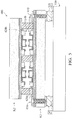
- Fig. 5 shows an intermediate stage of cross section of a method for forming a package structure of an embodiment of the invention.
- a carrier substrate 510 is provided, wherein the carrier substrate 510 may be a printed circuit board, a wafer, or a die.
- the carrier substrate 510 has a plurality of pads 512 thereon.
- the package structure 400 in Fig. 4B may be substantially vertically integrated with the carrier substrate 510 through bumps 520 therebetween.
- the first electronic device 114a and the second electronic device 114b are both electrically connected to the pads 512 of the carrier substrate 510 through the interconnection structures 410.
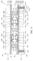
- Fig. 6 is a cross-sectional view of a package structure according to an embodiment of the present invention.
- a package structure 600 of the present embodiment is similar to the package structure 400 shown in Fig. 4B , except that the second semiconductor substrate 102b of the package structure 600 is a wafer. Specifically, the first semiconductor substrate 102a and the second semiconductor substrate 102b are both wafers.
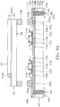
- Figs. 7A-7B show intermediate stages of cross sections of a method for forming a package structure of an embodiment of the invention.
- Figs. 7A-7B is similar to the method shown in Figs. 4A-4B , except that the second semiconductor device K2 (or the second semiconductor substrate 102b) in Figs. 7A-7B is reversed compared to the second semiconductor device K2 (or the second semiconductor substrate 102b) in Figs. 4A-4B .
- the third side S3 of the second semiconductor device K2 disposed with the second electronic devices 114b faces away from the first semiconductor device K1
- the fourth side S4 of the second semiconductor device K2 faces the first semiconductor device K1.
- the first semiconductor device K1 having the first semiconductor substrate 102a and the second semiconductor device K2 having the second semiconductor substrate 102b are provided.
- the first semiconductor substrate 102a may be a die or a wafer.
- Interconnection structures 710 are disposed in the second semiconductor device K2, wherein each of the interconnection structures 710 includes a via structure 132b and a first pad 130b.
- the via structure 132b is disposed in the via-hole 126b without exceeding the first opening 111b
- the first pad 130b is disposed on the third side S3 of the second semiconductor substrate 102b and covers the via-hole 126b, wherein the first pad 130b is adjoined to the via structure 132b and is electrically connected to the second electronic device 114b through the redistribution layer 420b.
- a portion of the first pad 130b extends into the via-hole 126b.
- the interconnection structure 710 may further include a second pad 134b covering the second opening 113b and be adjoined with the via structure 132b.
- the bumps 430b are disposed on and electrically connected to the second pads 134b.
- the first semiconductor device K1 is substantially vertically integrated with the second semiconductor device K2 by connecting the bumps 430b and the bumps 430a to constitute a package structure 700.
- the bumps 430b and the bumps 430a are connected to form bumps 430.
- the first electronic device 114a is electrically connected to the second electronic device 114b through the redistribution layer 420a, the bumps 430, the interconnection structure 710, and the redistribution layer 420b.
- the first electronic device 114a and the second electronic device 114b are both electrically connected to the interconnection structures 410 and 710.
- the first side 106 of the first semiconductor device K1 and the fourth side S4 of the second semiconductor device K2 face each other.
- the first side 106 of the first semiconductor device K1 is adjacent to the fourth side S4 of the second semiconductor device K2.
- Fig. 8 is a cross-sectional view of a package structure according to an embodiment of the present invention.
- a package structure 800 of the present embodiment is similar to the package structure 700 shown in Fig. 7B , except that the second semiconductor substrate 102b of the package structure 800 is a wafer.
- the first semiconductor substrate 102a and the second semiconductor substrate 102b of the package structure 800 are both wafers.
- the interconnection structures 410 and 710 may be aligned with each other, and the bumps 430 may be sandwiched between and connected to the interconnection structures 410 and 710.
- Figs. 9A-9B show intermediate stages of cross sections of a method for forming a package structure of an embodiment of the invention.
- the method shown in Figs. 9A-9B is similar to the method shown in Figs. 7A-7B , except that the second semiconductor device K2 in Figs. 9A-9B includes a source electrode layer S, a drain electrode layer D, and an active layer A sandwiched therebetween. Besides, the second electronic device 114b of the second semiconductor device K2 adjacent to the third side S3 is a gate electrode.
- the second electronic device 114b (i.e. the gate electrode) passes through the source electrode layer S, wherein an insulating layer (not shown) is disposed between the second electronic device 114b and the source electrode layer S and between the second electronic device 114b and the active layer A to electrically insulate the second electronic device 114b from the source electrode layer S and the active layer A.
- an insulating layer (not shown) is disposed between the second electronic device 114b and the source electrode layer S and between the second electronic device 114b and the active layer A to electrically insulate the second electronic device 114b from the source electrode layer S and the active layer A.
- the first semiconductor device K1 having the first semiconductor substrate 102a and the second semiconductor device K2 having the second semiconductor substrate 102b are provided.
- the first semiconductor substrate 102a may be a die or a wafer
- the second semiconductor substrate 102b may be a die.
- the bumps 430b are disposed on the fourth side S4 of the second semiconductor device K2 and are electrically connected to the drain electrode layer D.
- the first semiconductor device K1 is substantially vertically integrated with the second semiconductor device K2 by connecting the bumps 430b and the bumps 430a to constitute a package structure 900.
- the bumps 430b and the bumps 430a are connected to form bumps 430.
- the first electronic device 114a is electrically connected to the second semiconductor device K2 through the redistribution layer 420a and the bumps 430.
- the first electronic device 114a and the second semiconductor device K2 are both electrically connected to the interconnection structure 410.
- the first side 106 of the first semiconductor device K1 and the fourth side S4 of the second semiconductor device K2 face each other.
- the first side 106 of the first semiconductor device K1 is adjacent to the fourth side S4 of the second semiconductor device K2.
- Figs. 10A-10B show intermediate stages of cross sections of a method for forming a package structure of an embodiment of the invention.
- the method shown in Figs. 10A-10B is similar to the method shown in Figs. 9A-9B , except that the first semiconductor device K1 in Figs. 10A-10B is reversed compared to the first semiconductor device K1 in Figs. 9A-9B .
- the first side 106 of the first semiconductor device K1 disposed with the first electronic devices 114a faces away from the second semiconductor device K2
- the second side 108 of the first semiconductor device K1 faces the second semiconductor device K2.
- the first semiconductor device K1 having the first semiconductor substrate 102a and the second semiconductor device K2 having the second semiconductor substrate 102b are provided.
- the first semiconductor substrate 102a may be a die or a wafer
- the second semiconductor substrate 102b may be a die.
- the bumps 430a are disposed on and electrically connected to the second pads 134a.
- the first semiconductor device K1 is substantially vertically integrated with the second semiconductor device K2 by connecting the bumps 430b and the bumps 430a to constitute a package structure 1000.
- the bumps 430b and the bumps 430a are connected to form bumps 430.
- the first electronic device 114a is electrically connected to the second semiconductor device K2 through the redistribution layer 420a, the interconnection structure 410, and the bumps 430.
- the first electronic device 114a and the second semiconductor device K2 are both electrically connected to the interconnection structure 410.
- the second side 108 of the first semiconductor device K1 and the fourth side S4 of the second semiconductor device K2 face each other.
- the second side 108 of the first semiconductor device K1 is adjacent to the fourth side S4 of the second semiconductor device K2.
- the first electronic device 114a and the first pad 130a are both formed on the same side (i.e. the first side) as an exemplary example for illustration, and should not be adopted for limiting the present invention.
- the first electronic device 314 and the first pad 330 may be formed on different sides.
- the first electronic device 314 and the first pad 330 may be formed on the side 306 and the side 308, respectively.
- the passivation layer 322 may be formed on the side 306 to protect the first electronic device 314 thereunder.
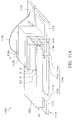
- Fig. 11A is a perspective drawing of a package structure according to an embodiment of the present invention.
- Fig. 11B is an equivalent-circuit diagram of the package structure shown in Fig. 11A .
- the package structure 1100 shown in Fig. 11A is similar to the package structure 1000 shown in Fig. 10B , except that the package structure 1100 shown in Fig. 11A further includes a lead frame 1110.
- the first semiconductor device K1 includes a HEMT device made of nitride-based semiconductor material and the second semiconductor device K2 includes a vertical transistor made of silicon-based material.
- the first and the second semiconductor devices K1 and K2 are stacked on the lead frame 1110.
- the lead frame 1110 has many portions 1112, 1114, 1116, 1118 and 1119 separated from each other.
- the first semiconductor device K1 is disposed on the lead frame 1110 and has a first semiconductor substrate 102a and a first electronic device 114a.
- the first electronic device 114a is a HEMT device disposed on an active region of the first semiconductor device K1.
- the first semiconductor device K1 further includes a passivation layer covering parts of the active region, the gate electrode 116a, the source electrode 118a, and the drain electrode 120a.
- the drain electrode 120a is disposed on and electrically connected to the portion 1112.
- the gate electrode 116a are disposed on and electrically connected to the portion 1114.
- the source electrode 118a is disposed on and electrically connected to the portion 1116.
- the portion 1112 or the portion 1114 can optionally cover parts of the passivation layer to enhance the field plate effect according to a requirement of product design.
- Interconnection structures 410 are disposed in the first semiconductor substrate 102a.
- the second semiconductor device K2 is disposed on the first semiconductor device K1.
- the second semiconductor device K2 comprises a second electronic device 114b.
- the second electronic device 114b is a vertical transistor including a source electrode S, a gate electrode G, and a drain electrode D, wherein the drain electrode D of the second electronice device 114b is electrically connected to the source electrode 118a of the first electronic device 114a through the interconnection structures 410.
- the source electrode S is electrically connected to the portion 1118 through a clip structure (e.g. a metal sheet) 1120 connected therebetween.
- the source electrode S of the second electronic device 114b is electrically connected to the gate electrode 116a of the first electronic devices 114a through the clip structure 1120 and a conductive path (not shown) inside the lead frame 1110.
- the gate electrode 114b is electrically connected to the portion 1119 through a bonding wire 1130 connected therebetween.
- the invention adopts the interconnection structure to replace conventional wires, and the interconnection structure has a better electrical performance than that of conventional wires, which benefits the performance of the package structure.
- the method for forming the interconnection structure of the invention forms the via structure using electroplating with the first pad as a seed layer, and no vacuum environment is required for forming the interconnect structure. Therefore, the method of the invention can produce semiconductor devices at a lower cost.
Landscapes
- Internal Circuitry In Semiconductor Integrated Circuit Devices (AREA)
- Engineering & Computer Science (AREA)
- Manufacturing & Machinery (AREA)
- Physics & Mathematics (AREA)
- Electromagnetism (AREA)
- Optics & Photonics (AREA)
Abstract
Description
- This application is a Continuation-In-Part of pending
U.S. patent application Ser. No. 13/675,297, filed Nov. 13, 2012 - This invention relates generally to semiconductor devices, and specifically, to package structures and methods for fabricating the same.
- Semiconductor components include external contacts that allow electrical connections to be made from the outside to the integrated circuits contained in the semiconductor components. A semiconductor die, for example, includes patterns of bond pads formed on the face of the die. Semiconductor packages, such as chip scale packages, also include external contacts. Typically, a component includes only one set of external contacts on either the face side (circuit side) or the back side of the component. However, it is sometimes necessary for a component to have external contacts on both sides.
- In semiconductor technology, a through-silicon via, also known as a through-substrate via, is a conductive feature formed in a semiconductor substrate (wafer or die) to electrically connect external contacts from both sides. The TSV feature vertically passes through the semiconductor substrate, providing for stacked wafer/die packaging methods and allowing for electrical connection between circuits within separate wafers or chips. There are a number of ways to create a TSV. Typically, a hole is etched into the semiconductor substrate, and sometimes through the interconnect structure as well. The hole may then be lined with various isolating layers and/or various metal layers. The hole is then filled with a conductive material, typically copper (Cu), which becomes the major part of a TSV.
- In traditional technologies, an electrode electroplating method is used for the conductive filling materials to be disposed in the hole of the through silicon via (TSV), wherein a seeding layer is formed by a vacuum technique, such as plasma vapor deposition, prior to formation of the conductive filling material. The vacuum technique requires high-priced equipment, which increases device costs.
- The invention provides a package structure including: a first semiconductor device including a first semiconductor substrate and a first electronic device, the first semiconductor device having a first side and a second side opposite to the first side, wherein at least part of the first electronic device being adjacent to the first side, and wherein the first semiconductor device has a via-hole formed through the first semiconductor device, wherein the via-hole has a first opening adjacent to the first side; an interconnection structure disposed in the first semiconductor device, wherein the interconnection structure comprises: a via structure disposed in the via-hole without exceeding the first opening; a first pad disposed on the first side of the first semiconductor device and covering the via-hole, wherein the first pad is adjoined to the via structure and is electrically connected to the first electronic device; and a second semiconductor device vertically integrated with the first semiconductor device, wherein the second semiconductor device comprises a second electronic device electrically connected with the first electronic device.
The invention provides a method of forming a package structure including: providing a first semiconductor device having a first side and a second side opposite to the first side; forming a via-hole through the first semiconductor device, wherein the via-hole has a first opening neighboring the first side and a second opening neighboring the second side; forming a first pad covering the first opening; forming a via structure in the via-hole subsequent to forming the first pad, wherein the via structure comprises a conductive material and is adjoined to the first pad; and substantially vertically integrating the first semiconductor device with a second semiconductor device. - The invention can be more fully understood by reading the subsequent detailed description and examples with references made to the accompanying drawings, wherein,
-
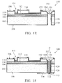
FIG. 1A to FIG. 1F show intermediate stages of cross sections of a method for forming a first semiconductor device with an interconnect structure of an embodiment of the invention. -
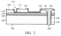
FIG. 2 show an intermediate stage of a cross section of a method for forming a first semiconductor device with an interconnect structure of an embodiment of the invention. -
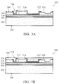
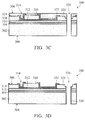
FIG. 3A to FIG. 3F show intermediate stages of cross sections of a method for forming a first semiconductor device with an interconnect structure of an embodiment of the invention. -
Figs. 4A-4B show intermediate stages of cross sections of a method for forming a package structure of an embodiment of the invention. -
Fig. 5 shows an intermediate stage of a cross section of a method for forming a package structure of an embodiment of the invention. -
Fig. 6 is a cross-sectional view of a package structure according to an embodiment of the present invention. -
Figs. 7A-7B show intermediate stages of cross sections of a method for forming a package structure of an embodiment of the invention. -
Fig. 8 is a cross-sectional view of a package structure according to an embodiment of the present invention. -
Figs. 9A-9B show intermediate stages of cross sections of a method for forming a package structure of an embodiment of the invention. -
Figs. 10A-10B show intermediate stages of cross sections of a method for forming a package structure of an embodiment of the invention. -
Fig. 11A is a perspective drawing of a package structure according to an embodiment of the present invention. -
Fig. 11B is an equivalent-circuit diagram of the package structure shown inFig. 11A . - It is understood that specific embodiments are provided as examples to teach the broader inventive concept, and one of ordinary skill in the art can easily apply the teaching of the present disclosure to other methods or apparatuses. The following discussion is only used to illustrate the invention, not limit the invention.
- A method for forming a
first semiconductor device 100 with an interconnection structure of an embodiment of the invention is illustrated in accordance withFIG. 1A to FIG. 1F . First, referring toFIG. 1A , afirst semiconductor device 100 is provided. Thefirst semiconductor device 100 includes afirst side 106 and asecond side 108 opposite to thefirst side 106. Thefirst semiconductor device 100 includes asubstrate 102. Thesubstrate 102 can be any suitable semiconductor material. For example, thesubstrate 102 can be Si, SiC, Ge, SiGe, GaAs, InAs, InP or GaN. Next, abuffer layer 104 is formed on thesubstrate 102. In an embodiment of the invention, thebuffer layer 104 can be a nitride based material to provide good adhesion for the layers thereon and also solve issues of lattice mismatch, but the invention is not limited thereto. Thebuffer layer 104 can be formed of any suitable material. In an embodiment of the invention, thebuffer layer 104 can be aluminum nitride. Achannel layer 110 and abarrier layer 112 are formed on thebuffer layer 104. In an embodiment, thechannel layer 110 can be GaN and thebarrier layer 112 can be AlGaN. Thereafter, a first metal layer (not shown) is formed on thechannel layer 110 and is then patterned by lithography and etching to form asource electrode 118 and adrain electrode 120. In an embodiment of the invention, the first metal layer is a stack of Ti, Al, Ni and/or Au layers. Furthermore, a rapid thermal annealing (RTA) process can be performed to the first metal layer. A second metal layer (not shown) is deposited on thechannel layer 110 and then patterned by lithography and etching to form agate electrode 116. Next, apassivation layer 122, such as a silicon nitride or silicon oxide layer, is formed to protect the device thereunder. Thechannel layer 110, thebarrier layer 112, thegate electrode 116, thesource electrode 118, and thedrain electrode 120 constitute anelectronic device 114 adjacent to thefirst side 106 of thefirst semiconductor device 100. In the embodiment, theelectronic device 114 is disposed at thefirst side 106 of thefirst semiconductor device 100, but the invention is not limited thereto. Theelectronic device 114 can be disposed at thesecond side 108 of thefirst semiconductor device 100. Furthermore, in the embodiment, theelectronic device 114 is a nitride-based semiconductor device. However, the invention is not limited to a nitride-based semiconductor device. The invention can be applied to any semiconductor device, such as a silicon based device, III-V group device and/or SOI device. - Next, referring to
FIG. 1B , aphotosensitive layer 124 is formed over thesubstrate 102 and theelectronic device 114. Thereafter, referring toFIG. 1C , thephotosensitive layer 124 is patterned by a lithography process and thesubstrate 102 is further etched using the patternedphotosensitive layer 124 as a mask to form a via-hole 126 extending through thesubstrate 102. In an embodiment, the via-hole 126 can be formed with drilling using a laser beam. - Referring to
FIG. 1D , thephotoresist layer 124 is then removed. In an embodiment, an insulatinglayer 128 is optionaly formed on the sidewall of the via-hole 126 for protection. In an embodiment, the insulatinglayer 128 is silicon oxide and can be formed by thermal oxidation or liquid phase deposition (LPD). The via-hole 126 has afirst opening 111 neighboring thefirst side 106 and asecond opening 113 neighboring thesecond side 108. - Referring to
FIGS. 1E∼1F , afirst pad 130 is formed on thefirst side 106 of thefirst semiconductor device 100 and covers thefirst opening 111 of the via-hole 126. Thefirst pad 130 can electrically connect to theelectrical device 114 and asecond pad 134 formed in subsequent steps, and can comprise a protrusion portion extending into the via-hole 126. In an embodiment, thefirst pad 130 can comprise silver paste and can be formed by screen printing. Referring toFIG. 1F , an electroplating process is performed using thefirst pad 130 as a seed layer to deposit a viastructure 132 which fills the via-hole 126. In an embodiment, the viastructure 132 and thefirst pad 130 comprises the same material. In another embodiment, the viastructure 132 and thefirst pad 130 comprises different materials. For example, the viastructure 132 can comprise copper. As shown inFIG. 1F , since the viastructure 132 is formed sequentially after forming thefirst pad 130, the viastructure 132 does not exceed thefirst opening 111 of the via-hole 126 neighboring thefirst side 106 of the first semiconductor device, but can exceed thesecond opening 113 of the via-hole 126 neighboring thesecond side 108 of the first semiconductor device. Next, asecond pad 134 is formed on thesecond side 108 of thefirst semiconductor device 100. In an embodiment, thesecond pad 134 can comprise silver paste and can be formed by screen printing. - In
Fig. 1F , thefirst semiconductor device 100 includes thesemiconductor substrate 102 and anelectronic device 114. Thefirst semiconductor device 100 has thefirst side 106 and thesecond side 108 opposite to thefirst side 106. At least part of theelectronic device 114 is adjacent to thefirst side 106. Thefirst semiconductor device 100 has the via-hole 126 formed through thefirst semiconductor device 100, wherein the via-hole 126 has thefirst opening 111 adjacent to thefirst side 106. - An interconnection structure C is disposed in the
first semiconductor device 100, wherein the interconnection structure C includes the viastructure 132 and thefirst pad 130. The viastructure 132 is disposed in the via-hole 126 without exceeding thefirst opening 111. Thefirst pad 130 is disposed on thefirst side 106 of thefirst semiconductor device 100 and covers the via-hole 126, wherein thefirst pad 130 is adjoined to the viastructure 132 and is electrically connected to theelectronic device 114. - In an embodiment of the invention, the
electrical device 114 is a high electron mobility transistor (HEMT) and thesubstrate 102 comprises a semiconductor substrate. Thesource electrode 118 is electrically connected to the semiconductor substrate through the viastructure 132. - A method for forming a first semiconductor device of another embodiment of the invention is illustrated in accordance with
FIG. 2 . The embodiment of the method for forming the first semiconductor device ofFIG. 2 is similar to the method ofFIGS. 1E∼1F and for simplicity its detailed descriptions of similar steps are omitted. The method for forming the first semiconductor device ofFIG. 2 is different from the method for forming the first semiconductor device ofFIGS. 1E∼1F in that thefirst pad 202 and the viastructure 204 are formed by a single step. In the embodiment, when the throughhole 126 depth is not great, for example the depth of the through hole is 10 µm to 200 µm, as shown inFIG. 2 , the screen print for forming thefirst pad 202 can also fill the throughhole 126, so that formation of thefirst pad 202 and the viastructure 204 can be performed by a single screen printing step. - A method for forming a first semiconductor device of yet another embodiment of the invention is illustrated in accordance with
FIG. 3A to FIG. 3F . The method of the embodiment illustrated inFIG. 3A to FIG. 3F differs from the embodiment illustrated inFIG. 1A to FIG. 1F by the forming of the pad on the second side of the substrate opposite to the first side with the electronic device prior to forming the via structure. First, referring toFIG. 3A , asemiconductor device 300 is provided. Thesemiconductor device 300 has afirst side 306 and asecond side 308. Thesemiconductor device 300 has asubstrate 302. Thesubstrate 302 can be any suitable semiconductor material. For example, thesubstrate 302 can be Si, SiC, Ge, SiGe, GaAs, InAs, InP or GaN. Next, abuffer layer 304 is formed on thesubstrate 302. In an embodiment of the invention, thebuffer layer 304 can be aluminum nitride. Achannel layer 310 and abarrier layer 312 are formed on thebuffer layer 304. In an embodiment, thechannel layer 310 can be GaN and thebarrier layer 312 can be AlGaN. Thereafter, a first metal layer (not shown) is formed on thechannel layer 310 and is then patterned by lithography and etching to form asource electrode 318 and adrain electrode 320. In an embodiment of the invention, the first metal layer is a stack of Ti, Al, Ni or Au layers. Furthermore, a rapid thermal annealing (RTA) process can be performed to the first metal layer. A second metal layer (not shown) is deposited and then patterned by lithography and etching to form agate electrode 316. Apassivation layer 322, such as silicon nitride and silicon oxide, is formed to protect the semiconductor device thereunder. Thechannel layer 310, thebarrier layer 312, thegate electrode 316, thesource electrode 318, and thedrain electrode 320 constitute anelectronic device 314 which is adjacent to thefirst side 306 of thesubstrate 302. In the embodiment, theelectronic device 314 is a nitride-based semiconductor device. However, the invention is not limited to being applied to a nitride-based semiconductor device. The invention can be applied to any semiconductor device, such as a silicon based device, III-V group device and/or SOI device. - Next, referring to
FIG. 3B , aphotosensitive layer 324 is formed over thesubstrate 302 to protect theelectronic device 314. Thereafter, referring toFIG. 3C , thephotosensitive layer 324 is patterned by a lithography process and thesubstrate 302 is further etched using the patternedphotosensitive layer 324 as a mask to form a via-hole 326 extending through thesubstrate 302 is formed. In an embodiment, the via-hole 326 can be formed by a laser beam. - Referring to
FIG. 3D , thephotoresist layer 324 is then removed. In an embodiment, an insulatinglayer 328 is optionally formed on the sidewall of the via-hole 326 for protection. In an embodiment, the insulatinglayer 328 is silicon oxide and can be formed by thermal oxidation or liquid phase deposition (LPD). - Referring to
FIG. 3E , afirst pad 330 is formed on thesecond side 308 of thesubstrate 302 and covers asecond opening 311 of the via-hole 326. In an embodiment, thefirst pad 330 can comprise silver paste and can be formed by screen printing. Referring toFIG. 3F , an electroplating process is performed using thefirst pad 330 as a seed layer to form a viastructure 332 which fills the via-hole 326. In an embodiment, the viastructure 332 and thefirst pad 330 comprise the same material. In another embodiment, the viastructure 332 and thefirst pad 330 comprise different materials. For example, the viastructure 332 can comprise copper. As shown inFIG. 3F , since the viastructure 332 is formed sequentially after forming thefirst pad 330, the viastructure 332 does not exceed of thesecond opening 311 neighboring thesecond side 308 of thesubstrate 302, but can exceed afirst opening 313 neighboring thefirst side 306 of thesubstrate 302. Next, asecond pad 334, such as silver, is formed on thefirst side 306 of thesubstrate 302. - In
Fig. 3F , thesemiconductor device 300 includes thesemiconductor substrate 302 and theelectronic device 314. Thesemiconductor device 300 has thefirst side 306 and thesecond side 308 opposite to thefirst side 306. At least part of theelectronic device 314 is adjacent to thefirst side 306. Thesemiconductor device 300 has the via-hole 326 formed through thesemiconductor device 300, wherein the via-hole 326 has thefirst opening 313 adjacent to thefirst side 306 and thesecond opening 311 adjacent to thesecond side 308. - An interconnection structure C1 is disposed in the
semiconductor device 300, wherein the interconnection structure C1 includes the viastructure 332 and thefirst pad 330. The viastructure 332 is disposed in the via-hole 326 without exceeding thefirst opening 311. Thefirst pad 330 is disposed on thesecond side 308 of thesemiconductor device 300 and covers the via-hole 326, wherein thefirst pad 330 is adjoined to the viastructure 332 and is electrically connected to theelectronic device 314. - The following description will illustrate embodiments of package structures adopting the semiconductor devices shown in
Figs. 1F ,2 and3F . -
Figs. 4A-4B show intermediate stages of cross sections of a method for forming a package structure of an embodiment of the invention. - It should be noted that, the elements in
Figs. 4A-4B , which are named and/or labeled identically to or similarly to those inFigs. 1A-3F , have materials, structures and/or manufacturing methods that are similar thereto. Therefore, the detailed descriptions are not repeated herein. - Referring to
Fig. 4A , a first semiconductor device K1 and a second semiconductor device K2 are provided. The first semiconductor device K1 has afirst side 106 and asecond side 108 opposite to thefirst side 106. The first semiconductor device K1 has afirst semiconductor substrate 102a and a plurality of firstelectronic devices 114a. Thefirst semiconductor substrate 102a is the same as thesubstrate 102 shown inFig. 1A . In the present embodiment, thefirst semiconductor substrate 102a may be a die or a wafer. - The first
electronic devices 114a are disposed on thefirst side 106. A plurality of via-holes 126a are formed through thefirst semiconductor substrate 102a, wherein each of the via-holes 126a has afirst opening 111 adjacent to thefirst side 106 and asecond opening 113 adjacent to thesecond side 108. The firstelectronic devices 114a may be a transistor and includes thechannel layer 110a, thebarrier layer 112a, thegate electrode 116a, thesource electrode 118a, and thedrain electrode 120a. -
Interconnection structures 410 are disposed in thefirst semiconductor substrate 102a, wherein each of theinterconnection structures 410 includes a viastructure 132a and afirst pad 130. Specifically, the viastructure 132a is disposed in the via-hole 126a without exceeding thefirst opening 111, and thefirst pad 130a is disposed on thefirst side 106 of thefirst semiconductor substrate 102a and covers the via-hole 126a, wherein thefirst pad 130a is adjoined to the viastructure 132a and is electrically connected to the firstelectronic device 114a. In one embodiment, a portion of thefirst pad 130a extends into the via-hole 126a. Theinterconnection structure 410 may further include asecond pad 134a covering thesecond opening 113 and be adjoined with the viastructure 132a. - Specifically, a
redistribution layer 420a is formed on thefirst side 106 to electrically connect thefirst pad 130a and the firstelectronic device 114a. A plurality ofbumps 430a may be formed on thefirst side 106 and may be electrically connected to thefirst pad 130a and the firstelectronic device 114a through theredistribution layer 420a. Thebumps 430a include copper, solder or other suitable materials. An under bump metallurgy (UBM)layer 432a may be formed between thebumps 430a and thechannel layer 110a. Apassivation layer 122a, such as silicon nitride and silicon oxide, is formed to protect the firstelectronic device 114a thereunder. - The second semiconductor device K2 has a third side S3 and a fourth side S4 opposite to the third side S3, and the second semiconductor device K2 includes a
second semiconductor substrate 102b (which is the same as thesubstrate 102 shown inFig. 1A ) and secondelectronic devices 114b disposed on thesecond semiconductor substrate 102b. The secondelectronic devices 114b are adjacent to the third side S3. - In the present embodiment, the
second semiconductor substrate 102b may be a die. The secondelectronic devices 114b may be a transistor and includes thechannel layer 110b, thebarrier layer 112b, thegate electrode 116b, thesource electrode 118b, and thedrain electrode 120b. - Specifically, a plurality of
bumps 430b may be formed on the third side S3. An under bump metallurgy (UBM)layer 432b may be formed between thebumps 430b and thechannel layer 110b. Aredistribution layer 420b is formed on the third side S3 to electrically connect thebumps 430b and the secondelectronic device 114b. Apassivation layer 122b, such as silicon nitride and silicon oxide, is formed to protect the secondelectronic device 114b thereunder. Thebumps 430b include copper, solder or other suitable materials. - Then, referring to
Fig. 4B , the first semiconductor device K1 (or thefirst semiconductor substrate 102a) is substantially vertically integrated with the second semiconductor device K2 (or thesecond semiconductor substrate 102b) by connecting thebumps 430b and thebumps 430a to constitute apackage structure 400. The connecting of thebumps 430b and thebumps 430a includes performing a reflow process. Thebumps 430b and thebumps 430a are connected to form bumps 430. - The first
electronic device 114a is electrically connected to the secondelectronic device 114b through theredistribution layer 420a, thebumps 430, and theredistribution layer 420b. The firstelectronic device 114a and the secondelectronic device 114b are both electrically connected to theinterconnection structure 410. - In the present embodiment, the
first side 106 of thefirst semiconductor substrate 102a and the third side S3 of thesecond semiconductor substrate 102b face each other. In other words, thefirst side 106 of thefirst semiconductor substrate 102a is adjacent to the third side S3 of thesecond semiconductor substrate 102b. - In
Fig. 4B , thepackage structure 400 is formed, wherein thepackage structure 400 includes the first semiconductor device K1, theinterconnection structure 410 and the second semiconductor device K2. - The first semiconductor device K1 includes the
first semiconductor substrate 102a and the firstelectronic devices 114a. The first semiconductor device K1 has thefirst side 106 and thesecond side 108 opposite to thefirst side 106. The firstelectronic devices 114a are adjacent to thefirst side 106. The first semiconductor device K1 has the via-holes 126a formed through the first semiconductor device K1, wherein each of the via-holes 126a has thefirst opening 111 adjacent to thefirst side 106. - The
interconnection structure 410 is disposed in the first semiconductor device K1, wherein theinterconnection structure 410 includes the viastructure 132a and thefirst pad 130a. The viastructure 132a is disposed in the via-hole 126a without exceeding thefirst opening 111. Thefirst pad 130a is disposed on thefirst side 106 of the first semiconductor device K1 and covers the via-hole 126a, wherein thefirst pad 130a is adjoined to the viastructure 132a and is electrically connected to theelectronic device 114a. - The second semiconductor device K2 is vertically integrated with the first semiconductor device K1, wherein the second semiconductor device K2 includes the second
electronic device 114b electrically connected with the firstelectronic device 114a. - It should be noted that the present embodiment adopts the
interconnection structure 410 to replace conventional wires (not shown), and theinterconnection structure 410 has an electrical performance better than that of conventional wires, which benefits the performance of thepackage structure 400. -
Fig. 5 shows an intermediate stage of cross section of a method for forming a package structure of an embodiment of the invention. Referring toFig. 5 , acarrier substrate 510 is provided, wherein thecarrier substrate 510 may be a printed circuit board, a wafer, or a die. Thecarrier substrate 510 has a plurality ofpads 512 thereon. Then, thepackage structure 400 inFig. 4B may be substantially vertically integrated with thecarrier substrate 510 throughbumps 520 therebetween. The firstelectronic device 114a and the secondelectronic device 114b are both electrically connected to thepads 512 of thecarrier substrate 510 through theinterconnection structures 410. -
Fig. 6 is a cross-sectional view of a package structure according to an embodiment of the present invention. Referring toFig. 6 , apackage structure 600 of the present embodiment is similar to thepackage structure 400 shown inFig. 4B , except that thesecond semiconductor substrate 102b of thepackage structure 600 is a wafer. Specifically, thefirst semiconductor substrate 102a and thesecond semiconductor substrate 102b are both wafers. -
Figs. 7A-7B show intermediate stages of cross sections of a method for forming a package structure of an embodiment of the invention. - It should be noted that the elements in
Figs. 7A-7B , which are named and/or labeled identically to or similarly to those inFigs. 1A-6 , have materials, structures and/or manufacturing methods that are similar thereto. Therefore, the detailed descriptions are not repeated herein. - It should be noted that the method shown in
Figs. 7A-7B is similar to the method shown inFigs. 4A-4B , except that the second semiconductor device K2 (or thesecond semiconductor substrate 102b) inFigs. 7A-7B is reversed compared to the second semiconductor device K2 (or thesecond semiconductor substrate 102b) inFigs. 4A-4B . Specifically, the third side S3 of the second semiconductor device K2 disposed with the secondelectronic devices 114b faces away from the first semiconductor device K1, and the fourth side S4 of the second semiconductor device K2 faces the first semiconductor device K1. - Referring to
Fig. 7A , the first semiconductor device K1 having thefirst semiconductor substrate 102a and the second semiconductor device K2 having thesecond semiconductor substrate 102b are provided. In the present embodiment, thefirst semiconductor substrate 102a may be a die or a wafer.Interconnection structures 710 are disposed in the second semiconductor device K2, wherein each of theinterconnection structures 710 includes a viastructure 132b and afirst pad 130b. - Specifically, the via
structure 132b is disposed in the via-hole 126b without exceeding thefirst opening 111b, and thefirst pad 130b is disposed on the third side S3 of thesecond semiconductor substrate 102b and covers the via-hole 126b, wherein thefirst pad 130b is adjoined to the viastructure 132b and is electrically connected to the secondelectronic device 114b through theredistribution layer 420b. In one embodiment, a portion of thefirst pad 130b extends into the via-hole 126b. Theinterconnection structure 710 may further include asecond pad 134b covering thesecond opening 113b and be adjoined with the viastructure 132b. Thebumps 430b are disposed on and electrically connected to thesecond pads 134b. - Then, referring to
Fig. 7B , the first semiconductor device K1 is substantially vertically integrated with the second semiconductor device K2 by connecting thebumps 430b and thebumps 430a to constitute apackage structure 700. Thebumps 430b and thebumps 430a are connected to form bumps 430. - The first
electronic device 114a is electrically connected to the secondelectronic device 114b through theredistribution layer 420a, thebumps 430, theinterconnection structure 710, and theredistribution layer 420b. The firstelectronic device 114a and the secondelectronic device 114b are both electrically connected to theinterconnection structures - In the present embodiment, the
first side 106 of the first semiconductor device K1 and the fourth side S4 of the second semiconductor device K2 face each other. In other words, thefirst side 106 of the first semiconductor device K1 is adjacent to the fourth side S4 of the second semiconductor device K2. -
Fig. 8 is a cross-sectional view of a package structure according to an embodiment of the present invention. Referring toFig. 8 , apackage structure 800 of the present embodiment is similar to thepackage structure 700 shown inFig. 7B , except that thesecond semiconductor substrate 102b of thepackage structure 800 is a wafer. Specifically, thefirst semiconductor substrate 102a and thesecond semiconductor substrate 102b of thepackage structure 800 are both wafers. Furthermore, theinterconnection structures bumps 430 may be sandwiched between and connected to theinterconnection structures -
Figs. 9A-9B show intermediate stages of cross sections of a method for forming a package structure of an embodiment of the invention. - It should be noted that the elements in
Figs. 9A-9B , which are named and/or labeled identically to or similarly to those inFigs. 1A-8 , have materials, structures and/or manufacturing methods that are similar thereto. Therefore, the detailed descriptions are not repeated herein. - It should be noted that the method shown in
Figs. 9A-9B is similar to the method shown inFigs. 7A-7B , except that the second semiconductor device K2 inFigs. 9A-9B includes a source electrode layer S, a drain electrode layer D, and an active layer A sandwiched therebetween. Besides, the secondelectronic device 114b of the second semiconductor device K2 adjacent to the third side S3 is a gate electrode. - Specifically, the second
electronic device 114b (i.e. the gate electrode) passes through the source electrode layer S, wherein an insulating layer (not shown) is disposed between the secondelectronic device 114b and the source electrode layer S and between the secondelectronic device 114b and the active layer A to electrically insulate the secondelectronic device 114b from the source electrode layer S and the active layer A. - Referring to
Fig. 9A , the first semiconductor device K1 having thefirst semiconductor substrate 102a and the second semiconductor device K2 having thesecond semiconductor substrate 102b are provided. In the present embodiment, thefirst semiconductor substrate 102a may be a die or a wafer, and thesecond semiconductor substrate 102b may be a die. Thebumps 430b are disposed on the fourth side S4 of the second semiconductor device K2 and are electrically connected to the drain electrode layer D. - Then, referring to
Fig. 9B , the first semiconductor device K1 is substantially vertically integrated with the second semiconductor device K2 by connecting thebumps 430b and thebumps 430a to constitute apackage structure 900. Thebumps 430b and thebumps 430a are connected to form bumps 430. - The first
electronic device 114a is electrically connected to the second semiconductor device K2 through theredistribution layer 420a and thebumps 430. The firstelectronic device 114a and the second semiconductor device K2 are both electrically connected to theinterconnection structure 410. - In the present embodiment, the
first side 106 of the first semiconductor device K1 and the fourth side S4 of the second semiconductor device K2 face each other. In other words, thefirst side 106 of the first semiconductor device K1 is adjacent to the fourth side S4 of the second semiconductor device K2. -
Figs. 10A-10B show intermediate stages of cross sections of a method for forming a package structure of an embodiment of the invention. - It should be noted that the elements in
Figs. 10A-10B , which are named and/or labeled identically to or similarly to those inFigs. 1A-9B , have materials, structures and/or manufacturing methods that are similar thereto. Therefore, the detailed descriptions are not repeated herein. - It should be noted that the method shown in
Figs. 10A-10B is similar to the method shown inFigs. 9A-9B , except that the first semiconductor device K1 inFigs. 10A-10B is reversed compared to the first semiconductor device K1 inFigs. 9A-9B . Specifically, thefirst side 106 of the first semiconductor device K1 disposed with the firstelectronic devices 114a faces away from the second semiconductor device K2, and thesecond side 108 of the first semiconductor device K1 faces the second semiconductor device K2. - Referring to
Fig. 10A , the first semiconductor device K1 having thefirst semiconductor substrate 102a and the second semiconductor device K2 having thesecond semiconductor substrate 102b are provided. In the present embodiment, thefirst semiconductor substrate 102a may be a die or a wafer, and thesecond semiconductor substrate 102b may be a die. Thebumps 430a are disposed on and electrically connected to thesecond pads 134a. - Then, referring to
Fig. 10B , the first semiconductor device K1 is substantially vertically integrated with the second semiconductor device K2 by connecting thebumps 430b and thebumps 430a to constitute apackage structure 1000. Thebumps 430b and thebumps 430a are connected to form bumps 430. - The first
electronic device 114a is electrically connected to the second semiconductor device K2 through theredistribution layer 420a, theinterconnection structure 410, and thebumps 430. The firstelectronic device 114a and the second semiconductor device K2 are both electrically connected to theinterconnection structure 410. - In the present embodiment, the
second side 108 of the first semiconductor device K1 and the fourth side S4 of the second semiconductor device K2 face each other. In other words, thesecond side 108 of the first semiconductor device K1 is adjacent to the fourth side S4 of the second semiconductor device K2. - It should be noted that, in the above embodiments, the first
electronic device 114a and thefirst pad 130a are both formed on the same side (i.e. the first side) as an exemplary example for illustration, and should not be adopted for limiting the present invention. In other embodiments (such as the embodiment ofFig. 3F ), the firstelectronic device 314 and thefirst pad 330 may be formed on different sides. For example, the firstelectronic device 314 and thefirst pad 330 may be formed on theside 306 and theside 308, respectively. Besides, thepassivation layer 322 may be formed on theside 306 to protect the firstelectronic device 314 thereunder. -
Fig. 11A is a perspective drawing of a package structure according to an embodiment of the present invention.Fig. 11B is an equivalent-circuit diagram of the package structure shown inFig. 11A . - It should be noted that the
package structure 1100 shown inFig. 11A is similar to thepackage structure 1000 shown inFig. 10B , except that thepackage structure 1100 shown inFig. 11A further includes alead frame 1110. - Specifically, as shown in
Figs. 11A and11B , the first semiconductor device K1 includes a HEMT device made of nitride-based semiconductor material and the second semiconductor device K2 includes a vertical transistor made of silicon-based material. The first and the second semiconductor devices K1 and K2 are stacked on thelead frame 1110. - The
lead frame 1110 hasmany portions lead frame 1110 and has afirst semiconductor substrate 102a and a firstelectronic device 114a. In this embodiment, the firstelectronic device 114a is a HEMT device disposed on an active region of the first semiconductor device K1. The first semiconductor device K1 further includes a passivation layer covering parts of the active region, thegate electrode 116a, thesource electrode 118a, and thedrain electrode 120a. Thedrain electrode 120a is disposed on and electrically connected to theportion 1112. Thegate electrode 116a are disposed on and electrically connected to theportion 1114. Thesource electrode 118a is disposed on and electrically connected to theportion 1116. Theportion 1112 or theportion 1114 can optionally cover parts of the passivation layer to enhance the field plate effect according to a requirement of product design. -
Interconnection structures 410 are disposed in thefirst semiconductor substrate 102a. The second semiconductor device K2 is disposed on the first semiconductor device K1. The second semiconductor device K2 comprises a secondelectronic device 114b. In this embodiment, the secondelectronic device 114b is a vertical transistor including a source electrode S, a gate electrode G, and a drain electrode D, wherein the drain electrode D of thesecond electronice device 114b is electrically connected to thesource electrode 118a of the firstelectronic device 114a through theinterconnection structures 410. The source electrode S is electrically connected to theportion 1118 through a clip structure (e.g. a metal sheet) 1120 connected therebetween. Specifically, the source electrode S of the secondelectronic device 114b is electrically connected to thegate electrode 116a of the firstelectronic devices 114a through theclip structure 1120 and a conductive path (not shown) inside thelead frame 1110. Thegate electrode 114b is electrically connected to theportion 1119 through abonding wire 1130 connected therebetween. - In view of the foregoing, the invention adopts the interconnection structure to replace conventional wires, and the interconnection structure has a better electrical performance than that of conventional wires, which benefits the performance of the package structure. Besides, the method for forming the interconnection structure of the invention forms the via structure using electroplating with the first pad as a seed layer, and no vacuum environment is required for forming the interconnect structure. Therefore, the method of the invention can produce semiconductor devices at a lower cost.
- While the invention has been described by way of example and in terms of the preferred embodiments, it is to be understood that the invention is not limited to the disclosed embodiments. It is intended to cover various modifications and similar arrangements (as would be apparent to those skilled in the art). Therefore, the scope of the appended claims should be accorded the broadest interpretation so as to encompass all such modifications and similar arrangements.
Claims (15)
- A package structure comprising:a first semiconductor device comprising a first semiconductor substrate and a first electronic device, the first semiconductor device having a first side and a second side opposite to the first side, wherein at least part of the first electronic device being adjacent to the first side, and wherein the first semiconductor device has a via-hole formed through the first semiconductor device, wherein the via-hole has a first opening adjacent to the first side;an interconnection structure disposed in the first semiconductor device, wherein the interconnection structure comprises:a via structure disposed in the via-hole without exceeding the first opening;a first pad disposed on the first side of the first semiconductor device and covering the via-hole, wherein the first pad is adjoined to the via structure and is electrically connected to the first electronic device; anda second semiconductor device vertically integrated with the first semiconductor device, wherein the second semiconductor device comprises a second electronic device electrically connected with the first electronic device.
- The package structure as claimed in claim 1, wherein the first semiconductor substrate comprises a die or a wafer, and the second semiconductor device comprises a second semiconductor substrate, wherein the second semiconductor substrate comprises a die or a wafer.
- The package structure as claimed in claim 1, wherein the second semiconductor device has a third side and a fourth side opposite to the third side, and wherein the second semiconductor device comprises a second semiconductor substrate adjacent to the fourth side and at least part of the second electronic device is adjacent to the third side.
- The package structure as claimed in claim 3, wherein the first side of the first semiconductor device or the second side of the first semiconductor device faces the third side of the second semiconductor device.
- The package structure as claimed in claim 3, wherein the first side of the first semiconductor device or the second side of the first semiconductor device faces the fourth side of the second semiconductor device.
- The package structure as claimed in claim 1, wherein at least one of the first electronic device and the second electronic device is a transistor.
- The package structure as claimed in claim 1, further comprising:a carrier substrate, wherein the first semiconductor device and the second semiconductor device are stacked on the carrier substrate, and the first electronic device and the second electronic device are electrically connected to the carrier substrate through the interconnection structure.
- The package structure as claimed in claim 1, wherein a portion of the first pad extends into the via-hole.
- A method of forming a package structure comprising:providing a first semiconductor device having a first side and a second side opposite to the first side;forming a via-hole through the first semiconductor device, wherein the via-hole has a first opening neighboring the first side and a second opening neighboring the second side;forming a first pad covering the first opening;forming a via structure in the via-hole subsequent to forming the first pad, wherein the via structure comprises a conductive material and is adjoined to the first pad; andsubstantially vertically integrating the first semiconductor device with a second semiconductor device.
- The method of forming the package structure as claimed in claim 9, further comprising:forming a second pad covering the second opening and adjoined with the via structure.
- The method of forming the package structure as claimed in claim 9, wherein the first semiconductor device comprising:a first semiconductor substrate;a first electronic device disposed on the first semiconductor substrate, at least part of the first electronic device being adjacent to the first side of the first semiconductor device; anda passivation layer disposed on the first semiconductor substrate and the first electronic device.
- The method of forming the package structure as claimed in claim 11, wherein the second semiconductor device has a third side and a fourth side opposite to the third side, and the second semiconductor device comprises a second semiconductor substrate and a second electronic device disposed on the second semiconductor substrate, at least part of the second electronic device being adjacent to the third side.
- The method of forming the package structure as claimed in claim 12, wherein the first semiconductor device is vertically integrated with the second semiconductor device while the first side of the first semiconductor device and the third side of the second semiconductor device face each other; or
wherein the first semiconductor device is vertically integrated with the second semiconductor device while the second side of the first semiconductor device and the third side of the second semiconductor device face each other. - The method of forming the package structure as claimed in claim 12, wherein the first semiconductor device is vertically integrated with the second semiconductor device while the second side of the first semiconductor device and the fourth side of the second semiconductor device face each other; or
wherein the first semiconductor device is vertically integrated with the second semiconductor device while the first side of the first semiconductor device and the fourth side of the second semiconductor device face each other. - The method of forming the package structure as claimed in claim 9, wherein the forming of the first pad comprises performing a screen printing process to form the first pad covering the first opening.
Applications Claiming Priority (1)
| Application Number | Priority Date | Filing Date | Title |
|---|---|---|---|
| US13/675,297 US9159699B2 (en) | 2012-11-13 | 2012-11-13 | Interconnection structure having a via structure |
Publications (2)
| Publication Number | Publication Date |
|---|---|
| EP2731132A2 true EP2731132A2 (en) | 2014-05-14 |
| EP2731132A3 EP2731132A3 (en) | 2017-05-17 |
Family
ID=49510038
Family Applications (2)
| Application Number | Title | Priority Date | Filing Date |
|---|---|---|---|
| EP13191021.8A Ceased EP2731132A3 (en) | 2012-11-13 | 2013-10-31 | Package structure and method of forming the same |
| EP13191022.6A Withdrawn EP2731133A3 (en) | 2012-11-13 | 2013-10-31 | Interconnection structure and fabrication thereof |
Family Applications After (1)
| Application Number | Title | Priority Date | Filing Date |
|---|---|---|---|
| EP13191022.6A Withdrawn EP2731133A3 (en) | 2012-11-13 | 2013-10-31 | Interconnection structure and fabrication thereof |
Country Status (4)
| Country | Link |
|---|---|
| US (2) | US9159699B2 (en) |
| EP (2) | EP2731132A3 (en) |
| CN (3) | CN103811465B (en) |
| TW (2) | TWI532130B (en) |
Cited By (6)
| Publication number | Priority date | Publication date | Assignee | Title |
|---|---|---|---|---|
| WO2016071366A1 (en) * | 2014-11-04 | 2016-05-12 | Commissariat à l'énergie atomique et aux énergies alternatives | Electronic power device with vertical 3d switching cell |
| EP3783663A1 (en) * | 2019-08-21 | 2021-02-24 | Infineon Technologies AG | Semiconductor device and method |
| CN114975322A (en) * | 2021-01-27 | 2022-08-30 | 英诺赛科(苏州)半导体有限公司 | Semiconductor device structure |
| EP4075515A1 (en) * | 2021-04-14 | 2022-10-19 | Exagan | Bi-directional device provided with a stack of two high electron mobility transistors connected head-to-tail |
| US12363932B2 (en) | 2021-05-05 | 2025-07-15 | Stmicroelectronics France | Electronic device provided with a stack of two high electron mobility transistors arranged in a bridge half-arm |
| US12513932B2 (en) | 2021-03-30 | 2025-12-30 | Stmicroelectronics France | Electronic device comprising two high electron mobility transistors |
Families Citing this family (12)
| Publication number | Priority date | Publication date | Assignee | Title |
|---|---|---|---|---|
| KR20140073163A (en) * | 2012-12-06 | 2014-06-16 | 삼성전자주식회사 | Semiconductor device and method of forming the same |
| US9659851B2 (en) * | 2014-02-07 | 2017-05-23 | Marvell World Trade Ltd. | Method and apparatus for improving the reliability of a connection to a via in a substrate |
| KR20170011366A (en) * | 2015-07-22 | 2017-02-02 | 삼성전자주식회사 | Semiconductor chip and semiconductor package having same |
| CN109671773B (en) * | 2017-10-16 | 2020-05-05 | 苏州能讯高能半导体有限公司 | Semiconductor device and method for manufacturing the same |
| US10366982B2 (en) | 2017-11-30 | 2019-07-30 | Taiwan Semiconductor Manufacturing Co., Ltd. | Structure with embedded memory device and contact isolation scheme |
| WO2019150526A1 (en) * | 2018-02-01 | 2019-08-08 | 三菱電機株式会社 | Semiconductor device and production method therefor |
| US11004794B2 (en) | 2018-06-27 | 2021-05-11 | Taiwan Semiconductor Manufacturing Co., Ltd. | Partial barrier free vias for cobalt-based interconnects and methods of fabrication thereof |
| CN109300947B (en) * | 2018-09-28 | 2021-09-07 | 京东方科技集团股份有限公司 | Flexible display substrate, method for manufacturing the same, and display device |
| CN115207080A (en) * | 2021-04-14 | 2022-10-18 | 埃克斯甘公司 | Bi-directional device provided with two stacks of high electron mobility transistors connected head-to-tail |
| US11967519B2 (en) | 2021-05-11 | 2024-04-23 | Innoscience (suzhou) Semiconductor Co., Ltd. | Integrated semiconductor device and method for manufacturing the same |
| TWI813100B (en) * | 2021-12-17 | 2023-08-21 | 世界先進積體電路股份有限公司 | Semiconductor structure and manufacturing method of the same |
| US20250072024A1 (en) * | 2023-08-23 | 2025-02-27 | Globalfoundries U.S. Inc. | Transistor with thermal plug |
Family Cites Families (55)
| Publication number | Priority date | Publication date | Assignee | Title |
|---|---|---|---|---|
| US5447871A (en) * | 1993-03-05 | 1995-09-05 | Goldstein; Edward F. | Electrically conductive interconnection through a body of semiconductor material |
| US6620731B1 (en) | 1997-12-18 | 2003-09-16 | Micron Technology, Inc. | Method for fabricating semiconductor components and interconnects with contacts on opposing sides |
| TWI244571B (en) * | 2002-01-30 | 2005-12-01 | Sanyo Electric Co | Semiconductor display device |
| TW200306770A (en) * | 2002-02-22 | 2003-11-16 | Fujikura Ltd | Multilayer wiring board, base for multilayer wiring board, printed wiring board, and its manufacturing method |
| US7045861B2 (en) * | 2002-03-26 | 2006-05-16 | Semiconductor Energy Laboratory Co., Ltd. | Light-emitting device, liquid-crystal display device and method for manufacturing same |
| JP2004095849A (en) * | 2002-08-30 | 2004-03-25 | Fujikura Ltd | Method of manufacturing semiconductor substrate with through electrode, method of manufacturing semiconductor device with through electrode |
| JP3937993B2 (en) * | 2002-10-02 | 2007-06-27 | 日立電線株式会社 | Wiring board manufacturing method |
| US6828512B2 (en) * | 2002-10-08 | 2004-12-07 | Intel Corporation | Apparatus and methods for interconnecting components to via-in-pad interconnects |
| JP2004146748A (en) * | 2002-10-28 | 2004-05-20 | Alps Electric Co Ltd | Thin film capacitor element |
| EP1603170B1 (en) * | 2003-03-10 | 2018-08-01 | Toyoda Gosei Co., Ltd. | Method for manufacturing a solid-state optical element device |
| US6897148B2 (en) * | 2003-04-09 | 2005-05-24 | Tru-Si Technologies, Inc. | Electroplating and electroless plating of conductive materials into openings, and structures obtained thereby |
| JP3891299B2 (en) * | 2003-05-06 | 2007-03-14 | セイコーエプソン株式会社 | Semiconductor device manufacturing method, semiconductor device, semiconductor device, electronic device |
| GB0311251D0 (en) * | 2003-05-16 | 2003-06-18 | Koninkl Philips Electronics Nv | Method of manufacture recyclable electronic products and electronic products obtained by the method |
| US7919787B2 (en) * | 2003-06-27 | 2011-04-05 | Avago Technologies Ecbu Ip (Singapore) Pte. Ltd. | Semiconductor device with a light emitting semiconductor die |
| KR100493063B1 (en) * | 2003-07-18 | 2005-06-02 | 삼성전자주식회사 | BGA package with stacked semiconductor chips and manufacturing method thereof |
| US8084866B2 (en) * | 2003-12-10 | 2011-12-27 | Micron Technology, Inc. | Microelectronic devices and methods for filling vias in microelectronic devices |
| JP2005303258A (en) * | 2004-03-16 | 2005-10-27 | Fujikura Ltd | Device and manufacturing method thereof |
| JP4327644B2 (en) * | 2004-03-31 | 2009-09-09 | Necエレクトロニクス株式会社 | Manufacturing method of semiconductor device |
| US7498647B2 (en) * | 2004-06-10 | 2009-03-03 | Micron Technology, Inc. | Packaged microelectronic imagers and methods of packaging microelectronic imagers |
| KR100594716B1 (en) * | 2004-07-27 | 2006-06-30 | 삼성전자주식회사 | Cap wafer having a cavity, a semiconductor chip using the same, and a method of manufacturing the same |
| JP4803993B2 (en) * | 2004-11-09 | 2011-10-26 | ルネサスエレクトロニクス株式会社 | Manufacturing method of semiconductor device |
| US7476918B2 (en) * | 2004-11-22 | 2009-01-13 | Panasonic Corporation | Semiconductor integrated circuit device and vehicle-mounted radar system using the same |
| WO2007020805A1 (en) * | 2005-08-12 | 2007-02-22 | Semiconductor Energy Laboratory Co., Ltd. | Manufacturing method of semiconductor device |
| JP4758712B2 (en) * | 2005-08-29 | 2011-08-31 | 新光電気工業株式会社 | Manufacturing method of semiconductor device |
| US7772116B2 (en) * | 2005-09-01 | 2010-08-10 | Micron Technology, Inc. | Methods of forming blind wafer interconnects |
| KR100704915B1 (en) * | 2005-09-15 | 2007-04-09 | 삼성전기주식회사 | Printed Circuit Board with Fine Pattern and Manufacturing Method Thereof |
| US7633167B2 (en) * | 2005-09-29 | 2009-12-15 | Nec Electronics Corporation | Semiconductor device and method for manufacturing same |
| TW200733336A (en) * | 2006-02-17 | 2007-09-01 | Advanced Semiconductor Eng | Ball grid array package structure with identification marks and substrate thereof |
| US7741218B2 (en) * | 2007-02-27 | 2010-06-22 | Freescale Semiconductor, Inc. | Conductive via formation utilizing electroplating |
| JP2008305938A (en) * | 2007-06-07 | 2008-12-18 | Toshiba Corp | Semiconductor device, and manufacturing method thereof |
| WO2009023462A1 (en) * | 2007-08-10 | 2009-02-19 | Spansion Llc | Semiconductor device and method for manufacturing thereof |
| JP2009070966A (en) * | 2007-09-12 | 2009-04-02 | Toshiba Corp | Semiconductor device and manufacturing method thereof |
| JP5536322B2 (en) * | 2007-10-09 | 2014-07-02 | 新光電気工業株式会社 | Substrate manufacturing method |
| US8779570B2 (en) * | 2008-03-19 | 2014-07-15 | Stats Chippac Ltd. | Stackable integrated circuit package system |
| WO2010011177A1 (en) * | 2008-07-24 | 2010-01-28 | Agency For Science, Technology And Research | A substrate arrangement and a method of manufacturing a substrate arrangement |
| US7843072B1 (en) | 2008-08-12 | 2010-11-30 | Amkor Technology, Inc. | Semiconductor package having through holes |
| KR101002680B1 (en) * | 2008-10-21 | 2010-12-21 | 삼성전기주식회사 | Semiconductor package and manufacturing method thereof |
| JP2010103236A (en) * | 2008-10-22 | 2010-05-06 | Panasonic Corp | Nitride semiconductor device |
| JP5268618B2 (en) * | 2008-12-18 | 2013-08-21 | 株式会社東芝 | Semiconductor device |
| JP5308145B2 (en) * | 2008-12-19 | 2013-10-09 | ルネサスエレクトロニクス株式会社 | Semiconductor device |
| JP5471268B2 (en) * | 2008-12-26 | 2014-04-16 | 大日本印刷株式会社 | Through electrode substrate and manufacturing method thereof |
| US7932608B2 (en) * | 2009-02-24 | 2011-04-26 | Taiwan Semiconductor Manufacturing Company, Ltd. | Through-silicon via formed with a post passivation interconnect structure |
| KR101573934B1 (en) * | 2009-03-02 | 2015-12-11 | 엘지전자 주식회사 | Solar cell and manufacturing mehtod of the same |
| US8329578B2 (en) * | 2009-03-27 | 2012-12-11 | Taiwan Semiconductor Manufacturing Company, Ltd. | Via structure and via etching process of forming the same |
| CN101847597B (en) * | 2009-03-27 | 2013-12-04 | 台湾积体电路制造股份有限公司 | Integrated circuit structure |
| CN102185580A (en) * | 2010-01-18 | 2011-09-14 | 精工爱普生株式会社 | Electronic apparatus, method of manufacturing substrate, and method of manufacturing electronic apparatus |
| US8518746B2 (en) * | 2010-09-02 | 2013-08-27 | Stats Chippac, Ltd. | Semiconductor device and method of forming TSV semiconductor wafer with embedded semiconductor die |
| KR101688006B1 (en) * | 2010-11-26 | 2016-12-20 | 삼성전자주식회사 | Semiconductor devices |
| US20120146111A1 (en) * | 2010-12-14 | 2012-06-14 | Shu-Ming Chang | Chip package and manufacturing method thereof |
| CN102569144B (en) * | 2010-12-22 | 2015-05-13 | 中芯国际集成电路制造(上海)有限公司 | Through hole etching method |
| KR20120071921A (en) * | 2010-12-23 | 2012-07-03 | 한국전자통신연구원 | Composition for filling through silicon vias (tsvs), tsv filling method and substrate including tsv filling formed of the composition |
| JP5595524B2 (en) * | 2010-12-28 | 2014-09-24 | 京セラ株式会社 | Optical module and optical wiring board |
| KR101801137B1 (en) * | 2011-02-21 | 2017-11-24 | 삼성전자주식회사 | Semiconductor Devices and Methods of Fabricating the Same |
| KR101780423B1 (en) * | 2011-03-18 | 2017-09-22 | 삼성전자주식회사 | Semiconductor device and method of forming the same |
| US8546900B2 (en) * | 2011-06-09 | 2013-10-01 | Optiz, Inc. | 3D integration microelectronic assembly for integrated circuit devices |
-
2012
- 2012-11-13 US US13/675,297 patent/US9159699B2/en active Active
-
2013
- 2013-10-21 TW TW102137865A patent/TWI532130B/en not_active IP Right Cessation
- 2013-10-21 TW TW102137864A patent/TWI515859B/en active
- 2013-10-31 EP EP13191021.8A patent/EP2731132A3/en not_active Ceased
- 2013-10-31 EP EP13191022.6A patent/EP2731133A3/en not_active Withdrawn
- 2013-11-08 CN CN201310552017.3A patent/CN103811465B/en not_active Expired - Fee Related
- 2013-11-08 CN CN201910107660.2A patent/CN110085563A/en active Pending
- 2013-11-08 CN CN201310557121.1A patent/CN103811461A/en active Pending
-
2015
- 2015-06-24 US US14/748,811 patent/US10424508B2/en active Active
Non-Patent Citations (1)
| Title |
|---|
| None |
Cited By (12)
| Publication number | Priority date | Publication date | Assignee | Title |
|---|---|---|---|---|
| WO2016071366A1 (en) * | 2014-11-04 | 2016-05-12 | Commissariat à l'énergie atomique et aux énergies alternatives | Electronic power device with vertical 3d switching cell |
| US10083942B2 (en) | 2014-11-04 | 2018-09-25 | Commissariat A L'energie Atomique Et Aux Energies Alternatives | Electronic power device with vertical 3D switching cell |
| EP3783663A1 (en) * | 2019-08-21 | 2021-02-24 | Infineon Technologies AG | Semiconductor device and method |
| KR20210024431A (en) * | 2019-08-21 | 2021-03-05 | 인피니언 테크놀로지스 아게 | Semiconductor device and method |
| US11817482B2 (en) | 2019-08-21 | 2023-11-14 | Infineon Technologies Ag | Semiconductor device and method |
| US12471341B2 (en) | 2019-08-21 | 2025-11-11 | Infineon Technologies Ag | Method of fabricating a semiconductor device |
| CN114975322A (en) * | 2021-01-27 | 2022-08-30 | 英诺赛科(苏州)半导体有限公司 | Semiconductor device structure |
| US12513932B2 (en) | 2021-03-30 | 2025-12-30 | Stmicroelectronics France | Electronic device comprising two high electron mobility transistors |
| EP4075515A1 (en) * | 2021-04-14 | 2022-10-19 | Exagan | Bi-directional device provided with a stack of two high electron mobility transistors connected head-to-tail |
| FR3122036A1 (en) * | 2021-04-14 | 2022-10-21 | Exagan | BIDIRECTIONAL DEVICE PROVIDED WITH A STACK OF TWO TRANSISTORS WITH HIGH ELECTRONIC MOBILITY CONNECTED HEAD-TO-TO-TAIL |
| US12243937B2 (en) | 2021-04-14 | 2025-03-04 | Stmicroelectronics France | Bidirectional device provided with a stack of two high electron mobility transistors connected head-to-tail |
| US12363932B2 (en) | 2021-05-05 | 2025-07-15 | Stmicroelectronics France | Electronic device provided with a stack of two high electron mobility transistors arranged in a bridge half-arm |
Also Published As
| Publication number | Publication date |
|---|---|
| TWI532130B (en) | 2016-05-01 |
| CN103811465A (en) | 2014-05-21 |
| TW201419487A (en) | 2014-05-16 |
| TW201419470A (en) | 2014-05-16 |
| EP2731132A3 (en) | 2017-05-17 |
| CN103811461A (en) | 2014-05-21 |
| US9159699B2 (en) | 2015-10-13 |
| US20150294910A1 (en) | 2015-10-15 |
| EP2731133A2 (en) | 2014-05-14 |
| US20140131871A1 (en) | 2014-05-15 |
| CN110085563A (en) | 2019-08-02 |
| EP2731133A3 (en) | 2017-11-01 |
| US10424508B2 (en) | 2019-09-24 |
| CN103811465B (en) | 2019-07-16 |
| TWI515859B (en) | 2016-01-01 |
Similar Documents
| Publication | Publication Date | Title |
|---|---|---|
| TWI532130B (en) | Package structure and manufacturing method thereof | |
| US9275982B2 (en) | Method of forming interconnection structure of package structure | |
| KR20250039940A (en) | Semiconductor package and manufacturing method thereof | |
| US8120177B2 (en) | Wafer level package having a stress relief spacer and manufacturing method thereof | |
| US9123626B1 (en) | Integrated passive flip chip package | |
| US20220173077A1 (en) | Stacked die structure and method of fabricating the same | |
| US20110266683A1 (en) | Stackable Power MOSFET, Power MOSFET Stack, and Process of Manufacture | |
| JP2008311599A (en) | Mold reconfigurable wafer, stack package using the same, and manufacturing method thereof | |
| KR20090031828A (en) | Semiconductor wafer with through-hole vias on Saw Street with back side redistribution layer | |
| JP2009010312A (en) | Stack package and manufacturing method thereof | |
| CN111863630A (en) | Method of forming chip package structure | |
| CN105655312A (en) | Semiconductor including stress buffer material formed on low-K metalized system | |
| US9768135B2 (en) | Semiconductor device having conductive bump with improved reliability | |
| US11139282B2 (en) | Semiconductor package structure and method for manufacturing the same | |
| CN102037370A (en) | Method for manufacturing and testing an integrated electronic circuit | |
| JP2005251953A (en) | Semiconductor device | |
| CN103681609B (en) | Integrated circuit, chip package and the method being used for manufacturing integrated circuit | |
| US8907459B2 (en) | Three-dimensional semiconductor integrated circuit device and method of fabricating the same | |
| KR102634695B1 (en) | Chip package structure with ring structure and method for forming the same | |
| US7871857B1 (en) | Methods of forming multi-chip semiconductor substrates | |
| CN220341210U (en) | semiconductor structure | |
| CN111696943B (en) | Semiconductor device having a die pad with a bank-like structure | |
| KR20250054573A (en) | Semiconductor device |
Legal Events
| Date | Code | Title | Description |
|---|---|---|---|
| PUAI | Public reference made under article 153(3) epc to a published international application that has entered the european phase |
Free format text: ORIGINAL CODE: 0009012 |
|
| 17P | Request for examination filed |
Effective date: 20131031 |
|
| AK | Designated contracting states |
Kind code of ref document: A2 Designated state(s): AL AT BE BG CH CY CZ DE DK EE ES FI FR GB GR HR HU IE IS IT LI LT LU LV MC MK MT NL NO PL PT RO RS SE SI SK SM TR |
|
| AX | Request for extension of the european patent |
Extension state: BA ME |
|
| PUAL | Search report despatched |
Free format text: ORIGINAL CODE: 0009013 |
|
| AK | Designated contracting states |
Kind code of ref document: A3 Designated state(s): AL AT BE BG CH CY CZ DE DK EE ES FI FR GB GR HR HU IE IS IT LI LT LU LV MC MK MT NL NO PL PT RO RS SE SI SK SM TR |
|
| AX | Request for extension of the european patent |
Extension state: BA ME |
|
| RIC1 | Information provided on ipc code assigned before grant |
Ipc: H01L 23/48 20060101AFI20170412BHEP Ipc: H01L 21/768 20060101ALI20170412BHEP Ipc: H01L 25/065 20060101ALI20170412BHEP Ipc: H01L 23/485 20060101ALN20170412BHEP Ipc: H01L 21/60 20060101ALI20170412BHEP |
|
| STAA | Information on the status of an ep patent application or granted ep patent |
Free format text: STATUS: REQUEST FOR EXAMINATION WAS MADE |
|
| R17P | Request for examination filed (corrected) |
Effective date: 20171114 |
|
| RBV | Designated contracting states (corrected) |
Designated state(s): AL AT BE BG CH CY CZ DE DK EE ES FI FR GB GR HR HU IE IS IT LI LT LU LV MC MK MT NL NO PL PT RO RS SE SI SK SM TR |
|
| STAA | Information on the status of an ep patent application or granted ep patent |
Free format text: STATUS: EXAMINATION IS IN PROGRESS |
|
| 17Q | First examination report despatched |
Effective date: 20191119 |
|
| RAP1 | Party data changed (applicant data changed or rights of an application transferred) |
Owner name: ANCORA SEMICONDUCTORS INC. |
|
| RAP3 | Party data changed (applicant data changed or rights of an application transferred) |
Owner name: ANCORA SEMICONDUCTORS INC. |
|
| RAP3 | Party data changed (applicant data changed or rights of an application transferred) |
Owner name: ANCORA SEMICONDUCTORS INC. |
|
| STAA | Information on the status of an ep patent application or granted ep patent |
Free format text: STATUS: THE APPLICATION HAS BEEN REFUSED |
|
| 18R | Application refused |
Effective date: 20230706 |