EP2731116B1 - Electrical medium or high voltage switching device - Google Patents
Electrical medium or high voltage switching device Download PDFInfo
- Publication number
- EP2731116B1 EP2731116B1 EP12192466.6A EP12192466A EP2731116B1 EP 2731116 B1 EP2731116 B1 EP 2731116B1 EP 12192466 A EP12192466 A EP 12192466A EP 2731116 B1 EP2731116 B1 EP 2731116B1
- Authority
- EP
- European Patent Office
- Prior art keywords
- contact
- switching device
- empty slots
- contact fingers
- electrical switching
- Prior art date
- Legal status (The legal status is an assumption and is not a legal conclusion. Google has not performed a legal analysis and makes no representation as to the accuracy of the status listed.)
- Active
Links
Images
Classifications
-
- H—ELECTRICITY
- H01—ELECTRIC ELEMENTS
- H01H—ELECTRIC SWITCHES; RELAYS; SELECTORS; EMERGENCY PROTECTIVE DEVICES
- H01H1/00—Contacts
-
- H—ELECTRICITY
- H01—ELECTRIC ELEMENTS
- H01H—ELECTRIC SWITCHES; RELAYS; SELECTORS; EMERGENCY PROTECTIVE DEVICES
- H01H1/00—Contacts
- H01H1/12—Contacts characterised by the manner in which co-operating contacts engage
- H01H1/36—Contacts characterised by the manner in which co-operating contacts engage by sliding
- H01H1/38—Plug-and-socket contacts
- H01H1/385—Contact arrangements for high voltage gas blast circuit breakers
Definitions
- the invention relates to the field of medium and high voltage switching technologies and concerns an electrical switching device according to the independent claim, particularly for a use as an earthing device, a fast-acting earthing device, a circuit breaker or a disconnector switch in power distribution systems.
- Electrical switching devices are well known in the field of high voltage switching applications. They are e.g. used for interrupting a current when an electrical fault occurs.
- circuit breakers have the task of opening contacts and keeping them far apart from one another in order to avoid a current flow, even in case of high electrical potential originating from the electrical fault itself.
- high voltage refers to voltages higher than 72.5 kV and the term medium voltage refers to voltages between 1 kV and 72.5 kV.
- the electrical switching devices may have to be able to carry high nominal currents of 5000 A to 6300 A and to switch very high short circuit currents of 63 kA to 80 kA at very high voltages of 550 kV to 1200 kV.
- the electrical switching devices of today require many so-called contact fingers for the nominal current.
- the current When disconnecting a nominal current within the electrical switching devices, the current commutates from the nominal contacts of the electrical switching device to its arcing contacts.
- a prior art switching device is known from EP 0 844 631 A2 .
- an electrical switching device for medium or high voltage circuits having at least a nominal contact arrangement.
- Its nominal contact arrangement comprises at least a first nominal contact comprising a plurality of contact fingers forming a finger cage.
- the finger cage is concentric with respect to a longitudinal axis.
- the contact fingers are separated from one another by empty slots extending up to a free end of the contact fingers.
- the nominal contact arrangement further comprises at least a mating second nominal contact. At least one of the nominal contacts is movable parallel to the longitudinal axis and cooperates with the other nominal contact for closing and opening the electric switching device.
- the empty slots comprise first and second empty slots.
- the second empty slots are shorter than the first empty slots.
- the contact fingers are grouped in groups, with the fingers of each group being separated by second empty slots and the fingers of adjacent groups being separated by first empty slots.
- the contact fingers By grouping the contact fingers, the overall circumferential stiffness is increased, with the result that the bending of the contact fingers is avoided or at least reduced or minimized. It is noted here that the empty slots are necessary in order to decrease the radial stiffness of the first nominal contact and provide a certain elasticity such that the second nominal contact can mechanically contact the first nominal contact by force fit, that is, the second tube-shaped nominal contact is inserted into the finger cage by displacing the contact fingers radially outwards with respect to the longitudinal axis when the electrical switching device is closed. The required elasticity of the contact fingers is also advantageous in order to compensate for manufacturing tolerances of the nominal contacts.
- each group of contact fingers comprises at least two contact fingers. In another embodiment each group of contact fingers comprises at least three contact fingers.
- the electrical switching device can be designed in a flexible way by choosing a number of contact fingers per group such that they can withstand the specific currents flowing through them in that particular electrical switching device.
- the groups each have the same number of contact fingers. This advantageously ensures that the stiffness of the finger cage is evenly distributed for all contact fingers.
- the invention is described for the example of a high voltage circuit breaker, but the principles described in the following also apply for the usage of the invention in other switching devices, e.g. of the type mentioned in the "Background"-section, such as in an earthing switch, fast-acting earthing switch, disconnector, combined disconnector and earthing switch, load break switch, generator circuit breaker, and generally in any switch.
- the most preferred use is in switches for high voltage and medium voltage.
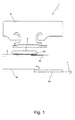
- Fig. 1 shows a partial sectional view of a simplified basic embodiment of a high voltage circuit breaker 1 in a closed configuration.
- "partial sectional view” means that only a part of the upper half of the circuit breaker is shown, for reasons of clarity.
- the device is rotationally symmetric about a longitudinal axis z. Only the elements of the circuit breaker 1 which are related to the present invention are described in the following, other elements present in the figures are not relevant for understanding the invention and are known by the skilled person in high voltage electrical engineering.
- a "closed configuration" as used herein means that nominal contacts of the circuit breaker are closed and are thus conducting a nominal current.
- the circuit breaker 1 comprises a chamber enclosed by a shell or enclosure 5 which normally is cylindrical around the longitudinal axis z. It further comprises a nominal contact arrangement formed by a first nominal contact comprising a plurality of contact fingers 3a, of which only one is shown here for reasons of clarity.
- the nominal contact arrangement is formed as a finger cage around the longitudinal axis z.
- the term "finger cage” as used herein refers to an arrangement, for example a cylindrical or conical or oval arrangement, of the contact fingers around the longitudinal axis z.
- a shielding 9 can be arranged around the finger cage.
- the nominal contact arrangement further comprises a second mating contact 3b which normally is a metal tube.
- the contact fingers 3a and the second contact 3b are movable relatively to one other from the closed configuration shown in Fig. 1 , in which they are in electrical contact to one another, into an opened configuration, in which they are apart from one another, and vice versa. It is also possible that only one of the contacts 3a, 3b moves parallel to the longitudinal axis z and the other contact 3b, 3a is stationary with respect to the longitudinal direction z.
- the contact fingers 3a are attached to or can be a part of a finger support 2, particularly a metal support cylinder 2.
- the circuit breaker 1 furthermore comprises an arcing contact arrangement formed by a first arcing contact 4a and a second arcing contact 4b.
- the first nominal contact and the first arcing contact 4a are typically not movable relatively to one another.
- the second nominal contact 3b and the second arcing contact 4b are not movable with respect to one another.
- the second nominal contact 3b and the second arcing contact 4b are moved parallel to the direction of the z-axis into the direction indicated by the z-arrow, such that the nominal contact arrangement disconnects first. Thereafter, the current commutates to the arcing contact arrangement, which is still closed. With further movement of the second nominal contact 3b and the second arcing contact 4b into the direction of the z-arrow, the arcing contact arrangement also disconnects, thereby creating an electric arc between the arcing contacts 4a, 4b, which is normally blasted out in a very short time.
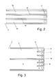
- Fig. 2 shows a detailed view of three contact fingers 3a of a finger cage of the high voltage circuit breaker 1 of Fig. 1 according to the prior art.
- This view shows the contact fingers 3a as they are seen "from within” the finger cage.
- the contact fingers 3a are attached to or can be a part of the finger support 2 of Fig. 1 .
- the contact fingers 3a are separated by empty slots 10, the purpose of which has been mentioned above.
- the contact areas 11 for the second nominal contact 4b (not shown) are denoted by the circles 11.
- the second nominal contact 3b contacts the contact fingers 3a in the area 11 of their free end.
- Fig. 3 shows a detailed view of two groups 5 of contact fingers 6, 7 of the finger cage of the high voltage circuit breaker of Fig. 1 according to the invention.
- the groups can comprise only two contact fingers 6, 7 or more than three contact fingers 6, 7, depending on the configuration of the circuit breaker 1.
- the groups of contact fingers 6, 7 are separated from each other by first empty slots 10, which are basically similar to those of the prior art configuration of Fig. 2 .
- the contact fingers 6, 7 of one group 5 are separated from each other by second empty slots 8 which are shorter than the first empty slots 10.
- each contact finger 6, 7 is adjacent to at least one second empty slot 8. Thus, there are no contact fingers which are adjacent to only first slots 10, which would again decrease their stiffness.
- the total number of the contact fingers 6, 7 is not a prime number. By this, it is ensured that all contact fingers 6, 7 can be grouped in suitable groups which all comprise the same number of fingers without occurrence of ungrouped contact fingers 6, 7. Of course, for this purpose the total number of contact fingers 6, 7 has to be a multiple of the number of contact fingers 6, 7 in one group 5.
- all the second empty slots 8 have the same length, whereas in another embodied of the invention the second empty slots 8 have different lengths.
- a largest length of the second empty slots 8 may advantageously exceed a smallest length of the second empty slots 8 by at least 20%.
- the second empty slots 8 are shorter than the first empty slots 10 by at least 50%. This ensures that both criteria, a good radial flexibility and a good circumferential stiffness, are met.
- the contact fingers 6, 7 are elastically deformed in a radial direction upon closing the electrical switching device, here the circuit breaker 1.
- the contact fingers 6, 7 form the finger cage.
- the contact fingers 6, 7 are formed by a tubular metal section.
- the first and second empty slots 10, 8 extend from a first end into the tubular metal section and the contact fingers 6, 7 are interconnected at a second end of the tubular metal section.
Landscapes
- Arc-Extinguishing Devices That Are Switches (AREA)
- Gas-Insulated Switchgears (AREA)
Description
- The invention relates to the field of medium and high voltage switching technologies and concerns an electrical switching device according to the independent claim, particularly for a use as an earthing device, a fast-acting earthing device, a circuit breaker or a disconnector switch in power distribution systems.
- Electrical switching devices are well known in the field of high voltage switching applications. They are e.g. used for interrupting a current when an electrical fault occurs. As an example for an electrical switching device, circuit breakers have the task of opening contacts and keeping them far apart from one another in order to avoid a current flow, even in case of high electrical potential originating from the electrical fault itself. For the purposes of this document the term high voltage refers to voltages higher than 72.5 kV and the term medium voltage refers to voltages between 1 kV and 72.5 kV. The electrical switching devices, like the circuit breakers, may have to be able to carry high nominal currents of 5000 A to 6300 A and to switch very high short circuit currents of 63 kA to 80 kA at very high voltages of 550 kV to 1200 kV.
- Because of the high nominal current, the electrical switching devices of today require many so-called contact fingers for the nominal current. When disconnecting a nominal current within the electrical switching devices, the current commutates from the nominal contacts of the electrical switching device to its arcing contacts.
- A prior art switching device is known from
EP 0 844 631 A2 . - It is an objective of the present invention to enhance an electrical switching device in terms of robustness by preventing damage to its contact fingers.
- This objective is solved by the features of
claim 1. Accordingly, an electrical switching device for medium or high voltage circuits having at least a nominal contact arrangement is provided. Its nominal contact arrangement comprises at least a first nominal contact comprising a plurality of contact fingers forming a finger cage. The finger cage is concentric with respect to a longitudinal axis. The contact fingers are separated from one another by empty slots extending up to a free end of the contact fingers. The nominal contact arrangement further comprises at least a mating second nominal contact. At least one of the nominal contacts is movable parallel to the longitudinal axis and cooperates with the other nominal contact for closing and opening the electric switching device. - In an ideal case all contact fingers of a known electrical switching device, e.g. a circuit breaker, would be separated from the mating nominal contact simultaneously. In practical embodiments of known circuit breakers or switches some of the contact fingers separate later than the rest of the contact fingers. Thus, before commuting to the arcing contact, the current still flows through the contact fingers that are still in contact with the mating nominal contact, for a period of time. It is only when these contact fingers have also lost contact with the mating nominal contact that the current switches to the arcing contacts. During the period when the entire current flows through the contact fingers which have separated later, significant electromagnetic forces act on these contact fingers and can deform them permanently. The deformation manifests itself in that adjacent fingers are attracted towards one another as a result of the Lorentz-force and may therefore be bent in a non-radial direction with respect to the longitudinal axis.
- Thus, in order to minimize the risk of damage, according to the invention the empty slots comprise first and second empty slots. The second empty slots are shorter than the first empty slots. Furthermore, the contact fingers are grouped in groups, with the fingers of each group being separated by second empty slots and the fingers of adjacent groups being separated by first empty slots.
- By grouping the contact fingers, the overall circumferential stiffness is increased, with the result that the bending of the contact fingers is avoided or at least reduced or minimized. It is noted here that the empty slots are necessary in order to decrease the radial stiffness of the first nominal contact and provide a certain elasticity such that the second nominal contact can mechanically contact the first nominal contact by force fit, that is, the second tube-shaped nominal contact is inserted into the finger cage by displacing the contact fingers radially outwards with respect to the longitudinal axis when the electrical switching device is closed. The required elasticity of the contact fingers is also advantageous in order to compensate for manufacturing tolerances of the nominal contacts.
- In an embodiment each group of contact fingers comprises at least two contact fingers. In another embodiment each group of contact fingers comprises at least three contact fingers.
- The higher the number of contact fingers is, the higher electromagnetic forces the contact fingers can withstand. Thus, the electrical switching device can be designed in a flexible way by choosing a number of contact fingers per group such that they can withstand the specific currents flowing through them in that particular electrical switching device.
- In yet another embodiment the groups each have the same number of contact fingers. This advantageously ensures that the stiffness of the finger cage is evenly distributed for all contact fingers.
- Further embodiments, advantages and applications of the invention result from the dependent claims and from the now following description by means of the figures. It is shown in:
-
Fig. 1 a partial sectional view of a simplified basic embodiment of a high voltage circuit breaker; -
Fig. 2 a detailed view, in radial direction, of three contact fingers of a finger cage of the high voltage circuit breaker ofFig. 1 according to the prior art; and -
Fig. 3 a detailed view, in radial direction, of two groups of contact fingers of the finger cage of the high voltage circuit breaker ofFig. 1 according to the invention. - The invention is described for the example of a high voltage circuit breaker, but the principles described in the following also apply for the usage of the invention in other switching devices, e.g. of the type mentioned in the "Background"-section, such as in an earthing switch, fast-acting earthing switch, disconnector, combined disconnector and earthing switch, load break switch, generator circuit breaker, and generally in any switch. The most preferred use is in switches for high voltage and medium voltage.
-
Fig. 1 shows a partial sectional view of a simplified basic embodiment of a highvoltage circuit breaker 1 in a closed configuration. InFig. 1 "partial sectional view" means that only a part of the upper half of the circuit breaker is shown, for reasons of clarity. The device is rotationally symmetric about a longitudinal axis z. Only the elements of thecircuit breaker 1 which are related to the present invention are described in the following, other elements present in the figures are not relevant for understanding the invention and are known by the skilled person in high voltage electrical engineering. - A "closed configuration" as used herein means that nominal contacts of the circuit breaker are closed and are thus conducting a nominal current.
- The
circuit breaker 1 comprises a chamber enclosed by a shell orenclosure 5 which normally is cylindrical around the longitudinal axis z. It further comprises a nominal contact arrangement formed by a first nominal contact comprising a plurality ofcontact fingers 3a, of which only one is shown here for reasons of clarity. The nominal contact arrangement is formed as a finger cage around the longitudinal axis z. The term "finger cage" as used herein refers to an arrangement, for example a cylindrical or conical or oval arrangement, of the contact fingers around the longitudinal axis z. Ashielding 9 can be arranged around the finger cage. The nominal contact arrangement further comprises asecond mating contact 3b which normally is a metal tube. Thecontact fingers 3a and thesecond contact 3b are movable relatively to one other from the closed configuration shown inFig. 1 , in which they are in electrical contact to one another, into an opened configuration, in which they are apart from one another, and vice versa. It is also possible that only one of thecontacts other contact - The
contact fingers 3a are attached to or can be a part of afinger support 2, particularly ametal support cylinder 2. - The
circuit breaker 1 furthermore comprises an arcing contact arrangement formed by a first arcingcontact 4a and a second arcingcontact 4b. - The first nominal contact and the first arcing
contact 4a are typically not movable relatively to one another. In the same way, the secondnominal contact 3b and the second arcingcontact 4b are not movable with respect to one another. For the explanatory purposes of the present invention it is assumed that only the secondnominal contact 3b and the arcingcontact 4b are movable and the finger cage is stationary along the z-axis. - When the closed circuit of
Fig. 1 shall be disconnected, the secondnominal contact 3b and thesecond arcing contact 4b are moved parallel to the direction of the z-axis into the direction indicated by the z-arrow, such that the nominal contact arrangement disconnects first. Thereafter, the current commutates to the arcing contact arrangement, which is still closed. With further movement of the secondnominal contact 3b and thesecond arcing contact 4b into the direction of the z-arrow, the arcing contact arrangement also disconnects, thereby creating an electric arc between the arcingcontacts -
Fig. 2 shows a detailed view of threecontact fingers 3a of a finger cage of the highvoltage circuit breaker 1 ofFig. 1 according to the prior art. This view shows thecontact fingers 3a as they are seen "from within" the finger cage. This also applies forFig. 3 . Thecontact fingers 3a are attached to or can be a part of thefinger support 2 ofFig. 1 . Thecontact fingers 3a are separated byempty slots 10, the purpose of which has been mentioned above. Furthermore, thecontact areas 11 for the secondnominal contact 4b (not shown) are denoted by thecircles 11. Thus, the secondnominal contact 3b contacts thecontact fingers 3a in thearea 11 of their free end. -
Fig. 3 shows a detailed view of twogroups 5 ofcontact fingers Fig. 1 according to the invention. In this configuration there are threecontact fingers group 5 ofcontact fingers contact fingers contact fingers circuit breaker 1. As can be seen, the groups ofcontact fingers empty slots 10, which are basically similar to those of the prior art configuration ofFig. 2 . Thecontact fingers group 5 are separated from each other by secondempty slots 8 which are shorter than the firstempty slots 10. - In embodiments, each
contact finger empty slot 8. Thus, there are no contact fingers which are adjacent to onlyfirst slots 10, which would again decrease their stiffness. - In embodiments, the total number of the
contact fingers contact fingers ungrouped contact fingers contact fingers contact fingers group 5. - In one embodiment of the invention all the second
empty slots 8 have the same length, whereas in another embodied of the invention the secondempty slots 8 have different lengths. In the latter case, a largest length of the secondempty slots 8 may advantageously exceed a smallest length of the secondempty slots 8 by at least 20%. These options make the finger cage more flexible in terms of construction. - In embodiments, the second
empty slots 8 are shorter than the firstempty slots 10 by at least 50%. This ensures that both criteria, a good radial flexibility and a good circumferential stiffness, are met. - The
contact fingers circuit breaker 1. - As mentioned, the
contact fingers contact fingers empty slots contact fingers - While there are shown and described presently preferred embodiments of the invention, it is to be distinctly understood that the invention is not limited thereto but may otherwise variously be embodied and practised within the scope of the following claims. Therefore, terms like "preferred" or "in particular" or "particularly" or "advantageously" signify optional and exemplary embodiments only.
-
- 1
- = basic circuit breaker
- 2
- = finger support
- 3a
- = contact finger of first nominal contact according to the prior art
- 3b
- = second nominal contact
- 4a
- = first arcing contact
- 4b
- = second arcing contact
- 5
- = group of contact fingers
- 6, 7
- = contact fingers according to the invention
- 8
- = second empty slot
- 9
- = shielding
- 10
- = first empty slot
- 11
- = contact areas
- z
- = longitudinal axis
Claims (12)
- Electrical switching device (1) for medium or high voltage circuits having at least a nominal contact arrangement, wherein the nominal contact arrangement comprisesa) at least a first nominal contact comprising a plurality of contact fingers (6, 7) forming a finger cage concentric with respect to a longitudinal axis (z), wherein the contact fingers (6, 7) are separated from one another by empty slots (10, 8) extending up to a free end of the contact fingers (6, 7), andb) at least a mating second nominal contact (3b),wherein at least one of the nominal contacts (6, 7; 3b) is movable parallel to the longitudinal axis (z) and cooperates with the other nominal contact (3b; 6, 7) for closing and opening the electric switching device (1),
characterized in that the empty slots comprise first and second empty slots (10, 8), wherein the second empty slots (8) are shorter than the first empty slots (10), and wherein the contact fingers (6, 7) are grouped in groups (5), with the contact fingers (6, 7) of each group (5) being separated by the second empty slots (8) and the contact fingers (6, 7) of adjacent groups (5) being separated by the first empty slots (10). - Electrical switching device according to claim 1, wherein each contact finger (6, 7) is adjacent to at least one of the second empty slots (8).
- Electrical switching device according to any one of the preceding claims, wherein each group (5) comprises at least two contact fingers (6, 7), in particular at least three contact fingers (6, 7).
- Electrical switching device according to any one of the preceding claims, wherein the groups (5) each have the same number of contact fingers (6, 7).
- Electrical switching device according to any one of the preceding claims, wherein a total number of the contact fingers (6, 7) is not a prime number.
- Electrical switching device according to any one of the preceding claims, wherein all of the second empty slots (8) have the same length.
- Electrical switching device according to one of the claims 1 to 5, wherein the second empty slots (8) have different lengths.
- Electrical switching device according to claim 7, wherein a largest length of the second empty slots (8) exceeds a smallest length of the second empty slots (8) by at least 20%.
- Electrical switching device according to any one of the preceding claims, wherein the second empty slots (8) are shorter than the first empty slots (10) by at least 50%.
- Electrical switching device according to any one of the preceding claims, wherein the contact fingers (6, 7) are elastically deformed in a radial direction upon closing the electrical switching device (1).
- Electrical switching device according to any one of the preceding claims, wherein the contact fingers (6, 7) are formed by a tubular metal section, wherein the first empty slots (10) and the second empty slots (8) extend from a first end into the tubular metal section, and wherein the contact fingers (6, 7) are interconnected at a second end of the tubular metal section.
- Electrical switching device according to any one of the preceding claims, it being an earthing switch, a fast-acting earthing switch, a disconnector, a combined disconnector and earthing switch, a load break switch, a circuit breaker, or a generator circuit breaker.
Priority Applications (4)
| Application Number | Priority Date | Filing Date | Title |
|---|---|---|---|
| EP12192466.6A EP2731116B1 (en) | 2012-11-13 | 2012-11-13 | Electrical medium or high voltage switching device |
| CA2833486A CA2833486C (en) | 2012-11-13 | 2013-11-12 | Electrical medium or high voltage switching device |
| CN201310726190.0A CN103811208B (en) | 2012-11-13 | 2013-11-13 | Medium-pressure or high pressure electrical switchgear |
| US14/079,068 US9627153B2 (en) | 2012-11-13 | 2013-11-13 | Electrical medium or high voltage switching device |
Applications Claiming Priority (1)
| Application Number | Priority Date | Filing Date | Title |
|---|---|---|---|
| EP12192466.6A EP2731116B1 (en) | 2012-11-13 | 2012-11-13 | Electrical medium or high voltage switching device |
Publications (2)
| Publication Number | Publication Date |
|---|---|
| EP2731116A1 EP2731116A1 (en) | 2014-05-14 |
| EP2731116B1 true EP2731116B1 (en) | 2015-06-17 |
Family
ID=47500884
Family Applications (1)
| Application Number | Title | Priority Date | Filing Date |
|---|---|---|---|
| EP12192466.6A Active EP2731116B1 (en) | 2012-11-13 | 2012-11-13 | Electrical medium or high voltage switching device |
Country Status (4)
| Country | Link |
|---|---|
| US (1) | US9627153B2 (en) |
| EP (1) | EP2731116B1 (en) |
| CN (1) | CN103811208B (en) |
| CA (1) | CA2833486C (en) |
Families Citing this family (2)
| Publication number | Priority date | Publication date | Assignee | Title |
|---|---|---|---|---|
| EP3091547B1 (en) | 2015-05-07 | 2018-07-04 | ABB Schweiz AG | Circuit breaker |
| CN110739163B (en) * | 2019-11-21 | 2025-03-25 | 北京博瑞莱智能科技集团有限公司 | On-load tap changer and transformer |
Family Cites Families (11)
| Publication number | Priority date | Publication date | Assignee | Title |
|---|---|---|---|---|
| US1978246A (en) * | 1933-03-31 | 1934-10-23 | Gen Electric | Electric circuit breaker |
| US3427419A (en) * | 1966-03-31 | 1969-02-11 | Westinghouse Electric Corp | Disconnecting contact assembly for electrical apparatus |
| US4012608A (en) * | 1974-08-20 | 1977-03-15 | Amp Incorporated | Miniature switch with substantial wiping action |
| US4319105A (en) * | 1976-12-27 | 1982-03-09 | Siemens-Allis, Inc. | High voltage air disconnect switch incorporating a puffer type load break switch |
| US4553008A (en) * | 1984-06-14 | 1985-11-12 | Cooper Industries, Inc. | Load interrupter |
| DE4212740C2 (en) * | 1992-04-16 | 1997-02-27 | Asea Brown Boveri | High voltage switch |
| JPH09147734A (en) * | 1995-11-27 | 1997-06-06 | Yazaki Corp | Fuse box |
| DE19648633A1 (en) * | 1996-11-25 | 1998-05-28 | Asea Brown Boveri | Electrical switching device |
| US7190245B2 (en) * | 2003-04-29 | 2007-03-13 | Medtronic, Inc. | Multi-stable micro electromechanical switches and methods of fabricating same |
| DE102004061276A1 (en) * | 2004-12-13 | 2006-06-22 | Siemens Ag | Electrical contact arrangement |
| CN2772008Y (en) * | 2005-01-21 | 2006-04-12 | 张臣义 | High-voltage isolator contact terminal-finger device |
-
2012
- 2012-11-13 EP EP12192466.6A patent/EP2731116B1/en active Active
-
2013
- 2013-11-12 CA CA2833486A patent/CA2833486C/en active Active
- 2013-11-13 US US14/079,068 patent/US9627153B2/en active Active
- 2013-11-13 CN CN201310726190.0A patent/CN103811208B/en active Active
Also Published As
| Publication number | Publication date |
|---|---|
| US9627153B2 (en) | 2017-04-18 |
| CN103811208B (en) | 2018-09-14 |
| US20140131183A1 (en) | 2014-05-15 |
| CA2833486A1 (en) | 2014-05-13 |
| EP2731116A1 (en) | 2014-05-14 |
| CN103811208A (en) | 2014-05-21 |
| CA2833486C (en) | 2020-06-30 |
Similar Documents
| Publication | Publication Date | Title |
|---|---|---|
| EP2110826B1 (en) | Racking of electrical distribution devices | |
| US20070246444A1 (en) | Contact system for an electrical switching device | |
| US10763060B2 (en) | Mechanical cut-off apparatus for a high-voltage or very high-voltage electric circuit with splitting device | |
| US11211209B2 (en) | Methods and systems for DC current interrupter based on thermionic arc extinction via anode ion depletion | |
| US11087940B2 (en) | Electrical interruption device | |
| WO2018167656A1 (en) | Vacuum switch | |
| CA2833486C (en) | Electrical medium or high voltage switching device | |
| EP3008746B1 (en) | Vacuum switching assembly | |
| JP6161621B2 (en) | Vacuum switch and its electrode assembly | |
| EP2920801B1 (en) | Contact system | |
| EP3286777B1 (en) | Bypass switch comprising a plunger, a first contact device and a second contact device | |
| EP2731117A1 (en) | High voltage electrical switching device with supporting tube | |
| EP3776616B1 (en) | Spring loaded auxiliary contact system for bus transfer switching in a center break switch | |
| EP2717283B1 (en) | Electrical switching device with multiple nominal contacts and method for manufacturing the electrical switching device | |
| AU2013347028B2 (en) | Contact system | |
| EP2698803A1 (en) | A circuit breaker | |
| JP2017034921A (en) | Switchgear | |
| US20160247638A1 (en) | Electrical contacts with a reduced aluminum section | |
| KR200475885Y1 (en) | gas insulated switchgear |
Legal Events
| Date | Code | Title | Description |
|---|---|---|---|
| PUAI | Public reference made under article 153(3) epc to a published international application that has entered the european phase |
Free format text: ORIGINAL CODE: 0009012 |
|
| 17P | Request for examination filed |
Effective date: 20121113 |
|
| AK | Designated contracting states |
Kind code of ref document: A1 Designated state(s): AL AT BE BG CH CY CZ DE DK EE ES FI FR GB GR HR HU IE IS IT LI LT LU LV MC MK MT NL NO PL PT RO RS SE SI SK SM TR |
|
| AX | Request for extension of the european patent |
Extension state: BA ME |
|
| R17P | Request for examination filed (corrected) |
Effective date: 20141114 |
|
| RBV | Designated contracting states (corrected) |
Designated state(s): AL AT BE BG CH CY CZ DE DK EE ES FI FR GB GR HR HU IE IS IT LI LT LU LV MC MK MT NL NO PL PT RO RS SE SI SK SM TR |
|
| GRAP | Despatch of communication of intention to grant a patent |
Free format text: ORIGINAL CODE: EPIDOSNIGR1 |
|
| INTG | Intention to grant announced |
Effective date: 20150120 |
|
| GRAS | Grant fee paid |
Free format text: ORIGINAL CODE: EPIDOSNIGR3 |
|
| GRAA | (expected) grant |
Free format text: ORIGINAL CODE: 0009210 |
|
| AK | Designated contracting states |
Kind code of ref document: B1 Designated state(s): AL AT BE BG CH CY CZ DE DK EE ES FI FR GB GR HR HU IE IS IT LI LT LU LV MC MK MT NL NO PL PT RO RS SE SI SK SM TR |
|
| REG | Reference to a national code |
Ref country code: GB Ref legal event code: FG4D |
|
| REG | Reference to a national code |
Ref country code: CH Ref legal event code: EP |
|
| REG | Reference to a national code |
Ref country code: AT Ref legal event code: REF Ref document number: 732330 Country of ref document: AT Kind code of ref document: T Effective date: 20150715 |
|
| REG | Reference to a national code |
Ref country code: IE Ref legal event code: FG4D |
|
| REG | Reference to a national code |
Ref country code: DE Ref legal event code: R096 Ref document number: 602012008010 Country of ref document: DE |
|
| PG25 | Lapsed in a contracting state [announced via postgrant information from national office to epo] |
Ref country code: HR Free format text: LAPSE BECAUSE OF FAILURE TO SUBMIT A TRANSLATION OF THE DESCRIPTION OR TO PAY THE FEE WITHIN THE PRESCRIBED TIME-LIMIT Effective date: 20150617 Ref country code: FI Free format text: LAPSE BECAUSE OF FAILURE TO SUBMIT A TRANSLATION OF THE DESCRIPTION OR TO PAY THE FEE WITHIN THE PRESCRIBED TIME-LIMIT Effective date: 20150617 Ref country code: LT Free format text: LAPSE BECAUSE OF FAILURE TO SUBMIT A TRANSLATION OF THE DESCRIPTION OR TO PAY THE FEE WITHIN THE PRESCRIBED TIME-LIMIT Effective date: 20150617 Ref country code: NO Free format text: LAPSE BECAUSE OF FAILURE TO SUBMIT A TRANSLATION OF THE DESCRIPTION OR TO PAY THE FEE WITHIN THE PRESCRIBED TIME-LIMIT Effective date: 20150917 |
|
| REG | Reference to a national code |
Ref country code: AT Ref legal event code: MK05 Ref document number: 732330 Country of ref document: AT Kind code of ref document: T Effective date: 20150617 |
|
| REG | Reference to a national code |
Ref country code: FR Ref legal event code: PLFP Year of fee payment: 4 |
|
| REG | Reference to a national code |
Ref country code: LT Ref legal event code: MG4D Ref country code: NL Ref legal event code: MP Effective date: 20150617 |
|
| PG25 | Lapsed in a contracting state [announced via postgrant information from national office to epo] |
Ref country code: RS Free format text: LAPSE BECAUSE OF FAILURE TO SUBMIT A TRANSLATION OF THE DESCRIPTION OR TO PAY THE FEE WITHIN THE PRESCRIBED TIME-LIMIT Effective date: 20150617 Ref country code: GR Free format text: LAPSE BECAUSE OF FAILURE TO SUBMIT A TRANSLATION OF THE DESCRIPTION OR TO PAY THE FEE WITHIN THE PRESCRIBED TIME-LIMIT Effective date: 20150918 Ref country code: LV Free format text: LAPSE BECAUSE OF FAILURE TO SUBMIT A TRANSLATION OF THE DESCRIPTION OR TO PAY THE FEE WITHIN THE PRESCRIBED TIME-LIMIT Effective date: 20150617 Ref country code: BG Free format text: LAPSE BECAUSE OF FAILURE TO SUBMIT A TRANSLATION OF THE DESCRIPTION OR TO PAY THE FEE WITHIN THE PRESCRIBED TIME-LIMIT Effective date: 20150917 |
|
| PG25 | Lapsed in a contracting state [announced via postgrant information from national office to epo] |
Ref country code: EE Free format text: LAPSE BECAUSE OF FAILURE TO SUBMIT A TRANSLATION OF THE DESCRIPTION OR TO PAY THE FEE WITHIN THE PRESCRIBED TIME-LIMIT Effective date: 20150617 |
|
| PG25 | Lapsed in a contracting state [announced via postgrant information from national office to epo] |
Ref country code: PT Free format text: LAPSE BECAUSE OF FAILURE TO SUBMIT A TRANSLATION OF THE DESCRIPTION OR TO PAY THE FEE WITHIN THE PRESCRIBED TIME-LIMIT Effective date: 20151019 Ref country code: CZ Free format text: LAPSE BECAUSE OF FAILURE TO SUBMIT A TRANSLATION OF THE DESCRIPTION OR TO PAY THE FEE WITHIN THE PRESCRIBED TIME-LIMIT Effective date: 20150617 Ref country code: PL Free format text: LAPSE BECAUSE OF FAILURE TO SUBMIT A TRANSLATION OF THE DESCRIPTION OR TO PAY THE FEE WITHIN THE PRESCRIBED TIME-LIMIT Effective date: 20150617 Ref country code: RO Free format text: LAPSE BECAUSE OF NON-PAYMENT OF DUE FEES Effective date: 20150617 Ref country code: SK Free format text: LAPSE BECAUSE OF FAILURE TO SUBMIT A TRANSLATION OF THE DESCRIPTION OR TO PAY THE FEE WITHIN THE PRESCRIBED TIME-LIMIT Effective date: 20150617 Ref country code: ES Free format text: LAPSE BECAUSE OF FAILURE TO SUBMIT A TRANSLATION OF THE DESCRIPTION OR TO PAY THE FEE WITHIN THE PRESCRIBED TIME-LIMIT Effective date: 20150617 Ref country code: AT Free format text: LAPSE BECAUSE OF FAILURE TO SUBMIT A TRANSLATION OF THE DESCRIPTION OR TO PAY THE FEE WITHIN THE PRESCRIBED TIME-LIMIT Effective date: 20150617 Ref country code: IS Free format text: LAPSE BECAUSE OF FAILURE TO SUBMIT A TRANSLATION OF THE DESCRIPTION OR TO PAY THE FEE WITHIN THE PRESCRIBED TIME-LIMIT Effective date: 20151017 |
|
| REG | Reference to a national code |
Ref country code: DE Ref legal event code: R097 Ref document number: 602012008010 Country of ref document: DE |
|
| PLBE | No opposition filed within time limit |
Free format text: ORIGINAL CODE: 0009261 |
|
| STAA | Information on the status of an ep patent application or granted ep patent |
Free format text: STATUS: NO OPPOSITION FILED WITHIN TIME LIMIT |
|
| PG25 | Lapsed in a contracting state [announced via postgrant information from national office to epo] |
Ref country code: IT Free format text: LAPSE BECAUSE OF FAILURE TO SUBMIT A TRANSLATION OF THE DESCRIPTION OR TO PAY THE FEE WITHIN THE PRESCRIBED TIME-LIMIT Effective date: 20150617 Ref country code: DK Free format text: LAPSE BECAUSE OF FAILURE TO SUBMIT A TRANSLATION OF THE DESCRIPTION OR TO PAY THE FEE WITHIN THE PRESCRIBED TIME-LIMIT Effective date: 20150617 |
|
| 26N | No opposition filed |
Effective date: 20160318 |
|
| PG25 | Lapsed in a contracting state [announced via postgrant information from national office to epo] |
Ref country code: MC Free format text: LAPSE BECAUSE OF FAILURE TO SUBMIT A TRANSLATION OF THE DESCRIPTION OR TO PAY THE FEE WITHIN THE PRESCRIBED TIME-LIMIT Effective date: 20150617 Ref country code: LU Free format text: LAPSE BECAUSE OF FAILURE TO SUBMIT A TRANSLATION OF THE DESCRIPTION OR TO PAY THE FEE WITHIN THE PRESCRIBED TIME-LIMIT Effective date: 20151113 |
|
| REG | Reference to a national code |
Ref country code: CH Ref legal event code: PL |
|
| PG25 | Lapsed in a contracting state [announced via postgrant information from national office to epo] |
Ref country code: CH Free format text: LAPSE BECAUSE OF NON-PAYMENT OF DUE FEES Effective date: 20151130 Ref country code: LI Free format text: LAPSE BECAUSE OF NON-PAYMENT OF DUE FEES Effective date: 20151130 |
|
| REG | Reference to a national code |
Ref country code: IE Ref legal event code: MM4A |
|
| PG25 | Lapsed in a contracting state [announced via postgrant information from national office to epo] |
Ref country code: SI Free format text: LAPSE BECAUSE OF FAILURE TO SUBMIT A TRANSLATION OF THE DESCRIPTION OR TO PAY THE FEE WITHIN THE PRESCRIBED TIME-LIMIT Effective date: 20150617 |
|
| PG25 | Lapsed in a contracting state [announced via postgrant information from national office to epo] |
Ref country code: IE Free format text: LAPSE BECAUSE OF NON-PAYMENT OF DUE FEES Effective date: 20151113 |
|
| REG | Reference to a national code |
Ref country code: FR Ref legal event code: PLFP Year of fee payment: 5 |
|
| PG25 | Lapsed in a contracting state [announced via postgrant information from national office to epo] |
Ref country code: BE Free format text: LAPSE BECAUSE OF FAILURE TO SUBMIT A TRANSLATION OF THE DESCRIPTION OR TO PAY THE FEE WITHIN THE PRESCRIBED TIME-LIMIT Effective date: 20150617 |
|
| REG | Reference to a national code |
Ref country code: DE Ref legal event code: R081 Ref document number: 602012008010 Country of ref document: DE Owner name: HITACHI ENERGY SWITZERLAND AG, CH Free format text: FORMER OWNER: ABB TECHNOLOGY AG, ZUERICH, CH Ref country code: DE Ref legal event code: R081 Ref document number: 602012008010 Country of ref document: DE Owner name: ABB SCHWEIZ AG, CH Free format text: FORMER OWNER: ABB TECHNOLOGY AG, ZUERICH, CH Ref country code: DE Ref legal event code: R081 Ref document number: 602012008010 Country of ref document: DE Owner name: ABB POWER GRIDS SWITZERLAND AG, CH Free format text: FORMER OWNER: ABB TECHNOLOGY AG, ZUERICH, CH Ref country code: DE Ref legal event code: R082 Ref document number: 602012008010 Country of ref document: DE Representative=s name: DENNEMEYER & ASSOCIATES S.A., DE Ref country code: DE Ref legal event code: R082 Ref document number: 602012008010 Country of ref document: DE Representative=s name: ZIMMERMANN & PARTNER PATENTANWAELTE MBB, DE |
|
| PG25 | Lapsed in a contracting state [announced via postgrant information from national office to epo] |
Ref country code: HU Free format text: LAPSE BECAUSE OF FAILURE TO SUBMIT A TRANSLATION OF THE DESCRIPTION OR TO PAY THE FEE WITHIN THE PRESCRIBED TIME-LIMIT; INVALID AB INITIO Effective date: 20121113 Ref country code: SM Free format text: LAPSE BECAUSE OF FAILURE TO SUBMIT A TRANSLATION OF THE DESCRIPTION OR TO PAY THE FEE WITHIN THE PRESCRIBED TIME-LIMIT Effective date: 20150617 |
|
| PG25 | Lapsed in a contracting state [announced via postgrant information from national office to epo] |
Ref country code: NL Free format text: LAPSE BECAUSE OF FAILURE TO SUBMIT A TRANSLATION OF THE DESCRIPTION OR TO PAY THE FEE WITHIN THE PRESCRIBED TIME-LIMIT Effective date: 20150617 Ref country code: SE Free format text: LAPSE BECAUSE OF FAILURE TO SUBMIT A TRANSLATION OF THE DESCRIPTION OR TO PAY THE FEE WITHIN THE PRESCRIBED TIME-LIMIT Effective date: 20150617 Ref country code: CY Free format text: LAPSE BECAUSE OF FAILURE TO SUBMIT A TRANSLATION OF THE DESCRIPTION OR TO PAY THE FEE WITHIN THE PRESCRIBED TIME-LIMIT Effective date: 20150617 |
|
| GBPC | Gb: european patent ceased through non-payment of renewal fee |
Effective date: 20161113 |
|
| PG25 | Lapsed in a contracting state [announced via postgrant information from national office to epo] |
Ref country code: MT Free format text: LAPSE BECAUSE OF FAILURE TO SUBMIT A TRANSLATION OF THE DESCRIPTION OR TO PAY THE FEE WITHIN THE PRESCRIBED TIME-LIMIT Effective date: 20150617 |
|
| REG | Reference to a national code |
Ref country code: FR Ref legal event code: PLFP Year of fee payment: 6 |
|
| PG25 | Lapsed in a contracting state [announced via postgrant information from national office to epo] |
Ref country code: GB Free format text: LAPSE BECAUSE OF NON-PAYMENT OF DUE FEES Effective date: 20161113 |
|
| PG25 | Lapsed in a contracting state [announced via postgrant information from national office to epo] |
Ref country code: MK Free format text: LAPSE BECAUSE OF FAILURE TO SUBMIT A TRANSLATION OF THE DESCRIPTION OR TO PAY THE FEE WITHIN THE PRESCRIBED TIME-LIMIT Effective date: 20150617 |
|
| REG | Reference to a national code |
Ref country code: FR Ref legal event code: TP Owner name: ABB SCHWEIZ AG, CH Effective date: 20180912 |
|
| PG25 | Lapsed in a contracting state [announced via postgrant information from national office to epo] |
Ref country code: AL Free format text: LAPSE BECAUSE OF FAILURE TO SUBMIT A TRANSLATION OF THE DESCRIPTION OR TO PAY THE FEE WITHIN THE PRESCRIBED TIME-LIMIT Effective date: 20150617 Ref country code: TR Free format text: LAPSE BECAUSE OF FAILURE TO SUBMIT A TRANSLATION OF THE DESCRIPTION OR TO PAY THE FEE WITHIN THE PRESCRIBED TIME-LIMIT Effective date: 20150617 |
|
| REG | Reference to a national code |
Ref country code: DE Ref legal event code: R081 Ref document number: 602012008010 Country of ref document: DE Owner name: HITACHI ENERGY SWITZERLAND AG, CH Free format text: FORMER OWNER: ABB SCHWEIZ AG, BADEN, CH Ref country code: DE Ref legal event code: R082 Ref document number: 602012008010 Country of ref document: DE Representative=s name: DENNEMEYER & ASSOCIATES RECHTSANWALTSGESELLSCH, DE Ref country code: DE Ref legal event code: R081 Ref document number: 602012008010 Country of ref document: DE Owner name: HITACHI ENERGY LTD, CH Free format text: FORMER OWNER: ABB SCHWEIZ AG, BADEN, CH Ref country code: DE Ref legal event code: R082 Ref document number: 602012008010 Country of ref document: DE Representative=s name: DENNEMEYER & ASSOCIATES S.A., DE Ref country code: DE Ref legal event code: R081 Ref document number: 602012008010 Country of ref document: DE Owner name: ABB POWER GRIDS SWITZERLAND AG, CH Free format text: FORMER OWNER: ABB SCHWEIZ AG, BADEN, CH |
|
| REG | Reference to a national code |
Ref country code: DE Ref legal event code: R081 Ref document number: 602012008010 Country of ref document: DE Owner name: HITACHI ENERGY SWITZERLAND AG, CH Free format text: FORMER OWNER: ABB POWER GRIDS SWITZERLAND AG, BADEN, CH Ref country code: DE Ref legal event code: R081 Ref document number: 602012008010 Country of ref document: DE Owner name: HITACHI ENERGY LTD, CH Free format text: FORMER OWNER: ABB POWER GRIDS SWITZERLAND AG, BADEN, CH |
|
| P01 | Opt-out of the competence of the unified patent court (upc) registered |
Effective date: 20230527 |
|
| REG | Reference to a national code |
Ref country code: DE Ref legal event code: R082 Ref document number: 602012008010 Country of ref document: DE Representative=s name: DENNEMEYER & ASSOCIATES RECHTSANWALTSGESELLSCH, DE Ref country code: DE Ref legal event code: R082 Ref document number: 602012008010 Country of ref document: DE Representative=s name: DENNEMEYER & ASSOCIATES S.A., DE Ref country code: DE Ref legal event code: R081 Ref document number: 602012008010 Country of ref document: DE Owner name: HITACHI ENERGY LTD, CH Free format text: FORMER OWNER: HITACHI ENERGY SWITZERLAND AG, BADEN, CH |
|
| REG | Reference to a national code |
Ref country code: DE Ref legal event code: R082 Ref document number: 602012008010 Country of ref document: DE Representative=s name: DENNEMEYER & ASSOCIATES RECHTSANWALTSGESELLSCH, DE |
|
| PGFP | Annual fee paid to national office [announced via postgrant information from national office to epo] |
Ref country code: DE Payment date: 20251119 Year of fee payment: 14 |
|
| PGFP | Annual fee paid to national office [announced via postgrant information from national office to epo] |
Ref country code: FR Payment date: 20251125 Year of fee payment: 14 |