EP2728702A2 - Power adapter for dynamically adjusting output voltage and power supply system with the same - Google Patents
Power adapter for dynamically adjusting output voltage and power supply system with the same Download PDFInfo
- Publication number
- EP2728702A2 EP2728702A2 EP20130163025 EP13163025A EP2728702A2 EP 2728702 A2 EP2728702 A2 EP 2728702A2 EP 20130163025 EP20130163025 EP 20130163025 EP 13163025 A EP13163025 A EP 13163025A EP 2728702 A2 EP2728702 A2 EP 2728702A2
- Authority
- EP
- European Patent Office
- Prior art keywords
- power
- voltage
- converting circuit
- circuit
- hub
- Prior art date
- Legal status (The legal status is an assumption and is not a legal conclusion. Google has not performed a legal analysis and makes no representation as to the accuracy of the status listed.)
- Granted
Links
Images


Classifications
-
- G—PHYSICS
- G06—COMPUTING OR CALCULATING; COUNTING
- G06F—ELECTRIC DIGITAL DATA PROCESSING
- G06F1/00—Details not covered by groups G06F3/00 - G06F13/00 and G06F21/00
- G06F1/26—Power supply means, e.g. regulation thereof
- G06F1/266—Arrangements to supply power to external peripherals either directly from the computer or under computer control, e.g. supply of power through the communication port, computer controlled power-strips
-
- G—PHYSICS
- G05—CONTROLLING; REGULATING
- G05F—SYSTEMS FOR REGULATING ELECTRIC OR MAGNETIC VARIABLES
- G05F1/00—Automatic systems in which deviations of an electric quantity from one or more predetermined values are detected at the output of the system and fed back to a device within the system to restore the detected quantity to its predetermined value or values, i.e. retroactive systems
- G05F1/10—Regulating voltage or current
-
- H—ELECTRICITY
- H02—GENERATION; CONVERSION OR DISTRIBUTION OF ELECTRIC POWER
- H02J—ELECTRIC POWER NETWORKS; CIRCUIT ARRANGEMENTS OR SYSTEMS FOR SUPPLYING OR DISTRIBUTING ELECTRIC POWER; SYSTEMS FOR STORING ELECTRIC ENERGY
- H02J7/00—Circuit arrangements for charging or discharging batteries or for supplying loads from batteries
- H02J7/02—Circuit arrangements for charging or discharging batteries or for supplying loads from batteries for charging batteries from AC mains by converters
- H02J7/04—Regulation of charging current or voltage
-
- H—ELECTRICITY
- H02—GENERATION; CONVERSION OR DISTRIBUTION OF ELECTRIC POWER
- H02M—APPARATUS FOR CONVERSION BETWEEN AC AND AC, BETWEEN AC AND DC, OR BETWEEN DC AND DC, AND FOR USE WITH MAINS OR SIMILAR POWER SUPPLY SYSTEMS; CONVERSION OF DC OR AC INPUT POWER INTO SURGE OUTPUT POWER; CONTROL OR REGULATION THEREOF
- H02M3/00—Conversion of DC power input into DC power output
- H02M3/02—Conversion of DC power input into DC power output without intermediate conversion into AC
- H02M3/04—Conversion of DC power input into DC power output without intermediate conversion into AC by static converters
- H02M3/10—Conversion of DC power input into DC power output without intermediate conversion into AC by static converters using discharge tubes with control electrode or semiconductor devices with control electrode
- H02M3/145—Conversion of DC power input into DC power output without intermediate conversion into AC by static converters using discharge tubes with control electrode or semiconductor devices with control electrode using devices of a triode or transistor type requiring continuous application of a control signal
- H02M3/155—Conversion of DC power input into DC power output without intermediate conversion into AC by static converters using discharge tubes with control electrode or semiconductor devices with control electrode using devices of a triode or transistor type requiring continuous application of a control signal using semiconductor devices only
- H02M3/156—Conversion of DC power input into DC power output without intermediate conversion into AC by static converters using discharge tubes with control electrode or semiconductor devices with control electrode using devices of a triode or transistor type requiring continuous application of a control signal using semiconductor devices only with automatic control of output voltage or current, e.g. switching regulators
-
- H—ELECTRICITY
- H02—GENERATION; CONVERSION OR DISTRIBUTION OF ELECTRIC POWER
- H02J—ELECTRIC POWER NETWORKS; CIRCUIT ARRANGEMENTS OR SYSTEMS FOR SUPPLYING OR DISTRIBUTING ELECTRIC POWER; SYSTEMS FOR STORING ELECTRIC ENERGY
- H02J2207/00—Details of circuit arrangements for charging or discharging batteries or supplying loads from batteries
- H02J2207/30—Charge provided using DC bus or data bus of a computer
-
- H—ELECTRICITY
- H02—GENERATION; CONVERSION OR DISTRIBUTION OF ELECTRIC POWER
- H02J—ELECTRIC POWER NETWORKS; CIRCUIT ARRANGEMENTS OR SYSTEMS FOR SUPPLYING OR DISTRIBUTING ELECTRIC POWER; SYSTEMS FOR STORING ELECTRIC ENERGY
- H02J7/00—Circuit arrangements for charging or discharging batteries or for supplying loads from batteries
- H02J7/90—Regulation of charging or discharging current or voltage
- H02J7/927—Regulation of charging or discharging current or voltage with introduction of pulses during the charging process
-
- H—ELECTRICITY
- H02—GENERATION; CONVERSION OR DISTRIBUTION OF ELECTRIC POWER
- H02M—APPARATUS FOR CONVERSION BETWEEN AC AND AC, BETWEEN AC AND DC, OR BETWEEN DC AND DC, AND FOR USE WITH MAINS OR SIMILAR POWER SUPPLY SYSTEMS; CONVERSION OF DC OR AC INPUT POWER INTO SURGE OUTPUT POWER; CONTROL OR REGULATION THEREOF
- H02M1/00—Details of apparatus for conversion
- H02M1/0003—Details of control, feedback or regulation circuits
- H02M1/0016—Control circuits providing compensation of output voltage deviations using feedforward of disturbance parameters
- H02M1/0019—Control circuits providing compensation of output voltage deviations using feedforward of disturbance parameters the disturbance parameters being load current fluctuations
Definitions
- the present invention relates to a power adapter, and more particularly to a power adapter for dynamically adjusting an output voltage.
- the present invention also relates to a power supply system with the power adapter.
- Each of the portable electronic devices is usually equipped with at least one first connecting port (e.g. USB port). Via the first connecting port, the portable electronic device is connected with a power supply system to receive a charging voltage.
- a first connecting port e.g. USB port
- the power supply system comprises a power adapter, a power cable, and a USB hub.
- the USB hub comprises plural second connecting ports (e.g. USB ports).
- the plural second connecting ports of the USB hub may be connected with the first connecting ports of corresponding portable electronic devices.
- the power adapter is used for receiving an input voltage (e.g. an AC voltage from a utility power source) and converting the input voltage into an output voltage (e.g. 5V) for powering the portable electronic devices.
- the power cable is connected between the power adapter and the USB hub. Through the power cable, the output voltage from the power adapter may be transmitted to the USB hub. After the first connecting ports of the portable electronic devices are connected with the second connecting ports of the USB hub, the electric energy of the output voltage may be transmitted to the portable electronic devices to charge the portable electronic devices.
- the length of the power cable is related to a corresponding impedance value of the power cable.
- the impedance value is increased. Since the level of the output voltage from the power adapter is fixed, the output voltage is subjected to a voltage drop. Due to the voltage drop, the voltage level at the USB hub is smaller than the level of the output voltage from the power adapter. Under this circumstance, the voltage level provided by the USB hub possibly fails to reach the desired voltage level for powering the portable electronic devices.
- the magnitude of a load current outputted from the power adapter is increased, and the voltage drop across the power cable is increased. Under this circumstance, the voltage level at the USB hub is further decreased.
- the voltage level provided by the USB hub possibly fails to reach the desired voltage level for powering the portable electronic devices. If the voltage level provided by the USB hub is insufficient, the chargeable batteries of the portable electronic devices fail to be fully charged and thus the aging conditions of the chargeable batteries are accelerated. Under this circumstance, the endurance of the chargeable batteries will be impaired.
- the present invention provides a power adapter for dynamically adjusting an output voltage and a power supply system with the power adapter.
- the power adapter is connected with a hub through a power cable.
- the power adapter comprises a power converting circuit, a current detecting circuit, and a controlling unit.
- a look-up table is stored in the controlling unit for recording a relationship between a load current and a voltage drop across an impedance of the power cable.
- the controlling unit may realize the magnitude of the load current and realize the voltage drop across the power cable according to the look-up table. Consequently, the power converting circuit is driven to increase the level of the output voltage to a magnitude equal to the sum of a charging voltage and the voltage drop.
- the voltage level provided by the hub possibly can reach the desired voltage level for powering the portable electronic devices.
- the portable electronic device can be normally operated and the use life of the chargeable battery within the portable electronic device can be extended.
- a power adapter connectable with a hub through a power cable.
- the hub has plural connecting ports.
- the power adapter includes a power converting circuit, a current detecting circuit, and a controlling unit.
- the power converting circuit is used for receiving an input voltage and converting the input voltage into an output voltage.
- the output voltage is outputted from an output terminal of the power adapter, and electric energy of the output voltage is transmitted to the hub through the power cable, so that a charging voltage with a constant voltage level is provided by the hub through the connecting ports.
- the current detecting circuit is connected with the power converting circuit for detecting a load current and outputting a corresponding current detecting signal.
- the load current is transmitted from the power converting circuit to the hub through the power cable.
- the controlling unit is connected with the current detecting circuit and the power converting circuit for receiving the current detecting signal.
- a look-up table is stored in the controlling unit for recording a relationship between the load current and a voltage drop across an impedance of the power cable. According to the current detecting signal and the look-up table, the controlling unit issues a feedback signal to the power converting circuit. According to the feedback signal, the power converting circuit is driven to dynamically adjust a level of the output voltage to be equal to the sum of the voltage drop and the charging voltage.
- a power supply system in accordance with another aspect of the present invention, there is provided a power supply system.
- the power supply system includes a power cable, a hub, and a power adapter.
- the hub is connected with the power cable, and includes at least one connecting port.
- the power adapter is connected with the hub through the power cable.
- the power adapter includes a power converting circuit, a current detecting circuit, and a controlling unit.
- the power converting circuit is used for receiving an input voltage and converting the input voltage into an output voltage.
- the output voltage is outputted from an output terminal of the power adapter, and electric energy of the output voltage is transmitted to the hub through the power cable, so that a charging voltage with a constant voltage level is provided by the hub through the connecting ports.
- the current detecting circuit is connected with the power converting circuit for detecting a load current and outputting a corresponding current detecting signal.
- the load current is transmitted from the power converting circuit to the hub through the power cable.
- the controlling unit is connected with the current detecting circuit and the power converting circuit for receiving the current detecting signal.
- a look-up table is stored in the controlling unit for recording a relationship between the load current and a voltage drop across an impedance of the power cable. According to the current detecting signal and the look-up table, the controlling unit issues a feedback signal to the power converting circuit. According to the feedback signal, the power converting circuit is driven to dynamically adjust a level of the output voltage to be equal to the sum of the voltage drop and the charging voltage.
- FIG. 1 is a schematic circuit diagram illustrating a power supply system according to an embodiment of the present invention
- FIG. 2 is a schematic circuit diagram illustrating a power supply system according to another embodiment of the present invention.
- FIG. 3 is a schematic circuit diagram illustrating the relationship between the current detecting circuit, the power converting circuit and the power cable of the power supply system of FIG. 1 ;
- FIG. 4 is a schematic detailed circuit diagram illustrating the hub of the power supply system of FIG. 1 .
- FIG. 1 is a schematic circuit diagram illustrating a power supply system according to an embodiment of the present invention.
- the power supply system 1 is detachably connected with at least one portable electronic device (not shown).
- the power supply system 1 is used for receiving an input voltage V in (e.g. an AC voltage from a utility power source) and converting the input voltage V in into a fixed charging voltage (e.g. 5V) for charging the at least one portable electronic device.
- V in e.g. an AC voltage from a utility power source
- a fixed charging voltage e.g. 5V
- the power supply system 1 comprises a power adapter 10, a power cable 11, and a hub 12.
- the hub 12 comprises plural connecting ports 120.
- the connecting ports 120 are USB ports.
- the charging voltage V c from the power supply system 1 may be transmitted to the corresponding portable electronic devices through the connecting ports 120 of the hub 12.
- a first end of the power cable 11 is connected with the hub 12, and a second end of the power cable 11 is detachably connected with the power adapter 10.
- the power adapter 10 is an AC/DC power adapter for receiving the AC input voltage V in and converting the AC input voltage V in into a DC output voltage V out .
- the power adapter 10 comprises a power converting circuit 100, a current detecting circuit 101, and a controlling unit 102.
- the power converting circuit 100 is an AC/DC power converting circuit.
- the power converting circuit 100 is connected between an input terminal and an output terminal of the power adapter 10.
- the input voltage V in is received by the power converting circuit 100.
- a switching circuit (not shown) within the power converting circuit 100, the AC input voltage V in is converted into the DC output voltage V out .
- the DC output voltage V out is outputted from the output terminal of the power adapter 10.
- the electric energy of the output voltage V out is transmitted to the hub 12 through the power cable 11.
- a load current I load is further outputted from the power converting circuit 100.
- the load current I load is also transmitted to the hub 12 through the power cable 11.
- the current detecting circuit 101 is connected with an output terminal of the power converting circuit 100 for detecting the load current I load and outputting a corresponding current detecting signal V i .
- the controlling unit 102 is connected with the current detecting circuit 101 and the power converting circuit 100.
- the current detecting signal V i is received by the controlling unit 102.
- the controlling unit 102 has a look-up table (not shown).
- the look-up table is previously stored in the controlling unit 102 before the power supply system 1 is produced.
- the look-up table records a relationship between the load current I load of the power converting circuit 100 and a voltage drop across a resistor R r of the power cable 11.
- the resistor R r has a constant impedance value. In a case that the load current I load is within a specified range, the relationships between different magnitudes of the load current I load are correlated with the voltage drops of flowing the load current I load through the resistor R r of the power cable 11.
- the controlling unit 102 issues a feedback signal V f to the power converting circuit 100.
- a level of the output voltage V out is dynamically adjusted by the power converting circuit 100.
- the controlling unit 102 comprises a micro controller 102a and a feedback circuit 102b.
- the micro controller 102a is connected with the feedback circuit 102b.
- the look-up table has been previously stored in the micro controller 102a.
- the micro controller 102a issues a control signal V s .
- the feedback circuit 102b is connected with the micro controller 102a and the power converting circuit 100.
- the feedback circuit 102b issues the feedback signal V f to the switching circuit of the power converting circuit 100.
- the feedback signal V f is a pulse width modulation (PWM) signal.
- PWM pulse width modulation
- the operations of the power supply system 1 will be illustrated with reference to FIG. 1 .
- the length of the power cable 11 is fixed, so that the impedance value of the resistor R r of the power cable 11 is fixed.
- the magnitudes of the load current I load are changed and the corresponding voltage drops across the resistor R r of the power cable 11 are measured.
- the relationships between the magnitudes of the load current I load and the corresponding voltage drops are correlated with each other and recorded as the look-up table. Consequently, the look-up table can be previously stored to the micro controller 102a of the controlling unit 102.
- the micro controller 102a may realize the magnitude of the load current I load according to the current detecting signal V i and realize the voltage drop of flowing the load current I load across the power cable 11 according to the look-up table.
- the power converting circuit 100 is driven to increase the level of the output voltage V out to a magnitude equal to the sum of the charging voltage V c and the voltage drop across the power cable 11.
- the charging voltage V c outputted from the connecting port 120 of the hub 12 can reach the desired voltage level for powering the portable electronic devices.
- the magnitude of the load current I load from the power converting circuit 100 is increased and the voltage drop of flowing the load current I load across the power cable 11 is increased.
- micro controller 102a may realize the magnitude of the load current I load according to the current detecting signal V i and realize the voltage drop of flowing the load current I load across the power cable 11 according to the look-up table.
- the power converting circuit 100 is driven to increase the level of the output voltage V out to a magnitude equal to the sum of the charging voltage V c and the voltage drop across the power cable 11.
- the power cable 11 comprises a positive wire and a negative wire (i.e. a ground wire).
- the power cable 11 comprises a positive wire, a negative wire (i.e. a ground wire), and a communication wire.
- the hub and the power adapter can be in communication with each other for exchanging signals.
- the power cable 11 is integrally formed with the hub 12. Under this circumstance, the power cable 11 fails to be detached from the hub 12.
- the power converting circuit 100 may fail to increase the level of the output voltage V out to a magnitude equal to the sum of the charging voltage V c and the voltage drop according to the feedback signal V f .
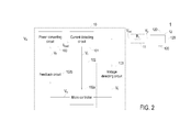
- the power adapter 10 further comprises a voltage detecting circuit 103.
- the voltage detecting circuit 103 is connected with the output terminal of the power converting circuit 100 and the output terminal of the power adapter 10.
- the voltage detecting circuit 103 is also connected with the controlling unit 102.
- the voltage detecting circuit 103 is used for detecting the output voltage V out and outputting a corresponding voltage detecting signal V t .
- the controlling unit 102 may judge whether the output voltage V out from the power converting circuit 100 complies with the contents of the look-up table (i.e. the corresponding load current I load ). That is, by judging whether the output voltage V out is equal to the sum of the charging voltage V c and the voltage drop, the controlling unit 102 may correspondingly adjust the feedback signal V f . If the level of the output voltage V out is lower than the sum of the charging voltage V c and the voltage drop, the adjusted feedback signal V f may further drive the power converting circuit 100 to increase the level of the output voltage V out to the sum of the charging voltage V c and the voltage drop. In other words, the voltage detecting circuit 103 is capable of confirming whether the output voltage V out is equal to the sum of the charging voltage V c and the voltage drop.
- FIG. 3 is a schematic circuit diagram illustrating the relationship between the current detecting circuit, the power converting circuit and the power cable of the power supply system of FIG. 1 .
- the current detecting circuit 101 comprises a detecting resistor R t and an error amplifier OP.
- the detecting resistor R t is connected between the power converting circuit 100 and the output terminal of the power adapter 10.
- An inverting input terminal of the error amplifier OP is connected with a first end of the detecting resistor R t and the power converting circuit 100 through a first resistor R 1 .
- a non-inverting input terminal of the error amplifier OP is connected with a second end of the detecting resistor R t through a second resistor R 2 .
- An output terminal of the error amplifier OP is connected with the controlling unit 102.
- the current detecting signal V i is outputted from the output terminal of the error amplifier OP.
- FIG. 4 is a schematic detailed circuit diagram illustrating the hub of the power supply system of FIG. 1 .
- the hub 12 further comprises plural overcurrent detectors 121, an overvoltage detector 122, a switching circuit 123, a micro controller 124, and a light-emitting unit 125.
- the switching circuit 123 is connected with a positive input terminal of the hub 12. Under control of the micro controller 124, the switching circuit 123 is alternately turned on and turned off. Consequently, during normal operations of the hub 12, the switching circuit 123 is turned on.
- the overvoltage detector 122 is connected with the positive input terminal of the hub 12 and the micro controller 124.
- the overvoltage detector 122 is used for detecting whether the input terminal of the hub 12 is suffered from an overvoltage condition. In a case that the input terminal of the hub 12 is suffered from the overvoltage condition, the overvoltage detector 122 issues an overvoltage notifying signal to the micro controller 124. In response to the overvoltage notifying signal, the switching circuit 123 is turned off under control of the micro controller 124. Under this circumstance, the electric energy from the power cable 11 fails to be received by the hub 12, so that the hub 12 is disabled.
- the plural overcurrent detectors 121 are connected with corresponding connecting ports 120. Each overcurrent detector 121 is used for detecting whether the corresponding connecting port 120 is suffered from an overcurrent condition.
- the corresponding overcurrent detector 121 issues an overcurrent notifying signal to the micro controller 124.
- the switching circuit 123 is turned off under control of the micro controller 124.
- the electric energy from the power cable 11 fails to be received by the hub 12, so that the hub 12 is disabled.
- the light-emitting unit 125 is connected with the micro controller 124.
- the switching circuit 123 is turned off under control of the micro controller 124, the light-emitting unit 125 is controlled by the micro controller 124 to emit a light beam in order to notify the user that the hub 12 is in the overvoltage condition or the overcurrent condition.
- the present invention provides a power adapter for dynamically adjusting an output voltage and a power supply system with the power adapter.
- the power adapter is connected with a hub through a power cable.
- the power adapter comprises a power converting circuit, a current detecting circuit, and a controlling unit.
- a look-up table is stored in the controlling unit for recording a relationship between a load current and a voltage drop across an impedance of the power cable.
- the controlling unit may realize the magnitude of the load current and realize the voltage drop across the power cable according to the look-up table. Consequently, the power converting circuit is driven to increase the level of the output voltage to a magnitude equal to the sum of a charging voltage and the voltage drop.
- the voltage level provided by the hub possibly can reach the desired voltage level for powering the portable electronic devices.
- the portable electronic device can be normally operated and the use life of the chargeable battery within the portable electronic device can be extended.
Landscapes
- Engineering & Computer Science (AREA)
- General Engineering & Computer Science (AREA)
- Theoretical Computer Science (AREA)
- Physics & Mathematics (AREA)
- General Physics & Mathematics (AREA)
- Power Engineering (AREA)
- Computer Hardware Design (AREA)
- Electromagnetism (AREA)
- Radar, Positioning & Navigation (AREA)
- Automation & Control Theory (AREA)
- Dc-Dc Converters (AREA)
- Charge And Discharge Circuits For Batteries Or The Like (AREA)
Abstract
Description
- The present invention relates to a power adapter, and more particularly to a power adapter for dynamically adjusting an output voltage. The present invention also relates to a power supply system with the power adapter.
- With increasing development of science and technology, portable electronic devices such as smart phones, tablet personal computers or MP3 players are now rapidly gaining in popularity. Generally, these portable electronic devices are powered by a fixed voltage (e.g. 5V). Each of the portable electronic devices is usually equipped with at least one first connecting port (e.g. USB port). Via the first connecting port, the portable electronic device is connected with a power supply system to receive a charging voltage.
- Generally, the power supply system comprises a power adapter, a power cable, and a USB hub. The USB hub comprises plural second connecting ports (e.g. USB ports). The plural second connecting ports of the USB hub may be connected with the first connecting ports of corresponding portable electronic devices. The power adapter is used for receiving an input voltage (e.g. an AC voltage from a utility power source) and converting the input voltage into an output voltage (e.g. 5V) for powering the portable electronic devices. The power cable is connected between the power adapter and the USB hub. Through the power cable, the output voltage from the power adapter may be transmitted to the USB hub. After the first connecting ports of the portable electronic devices are connected with the second connecting ports of the USB hub, the electric energy of the output voltage may be transmitted to the portable electronic devices to charge the portable electronic devices.
- As known, the length of the power cable is related to a corresponding impedance value of the power cable. As the length of the power cable is increased, the impedance value is increased. Since the level of the output voltage from the power adapter is fixed, the output voltage is subjected to a voltage drop. Due to the voltage drop, the voltage level at the USB hub is smaller than the level of the output voltage from the power adapter. Under this circumstance, the voltage level provided by the USB hub possibly fails to reach the desired voltage level for powering the portable electronic devices. Moreover, as the number of the portable electronic devices connected with the USB hub is increased, the magnitude of a load current outputted from the power adapter is increased, and the voltage drop across the power cable is increased. Under this circumstance, the voltage level at the USB hub is further decreased. Due to the impedance of the power cable, the voltage level provided by the USB hub possibly fails to reach the desired voltage level for powering the portable electronic devices. If the voltage level provided by the USB hub is insufficient, the chargeable batteries of the portable electronic devices fail to be fully charged and thus the aging conditions of the chargeable batteries are accelerated. Under this circumstance, the endurance of the chargeable batteries will be impaired.
- Therefore, there is a need of providing an improved power adapter for dynamically adjusting an output voltage in order to obviate the above drawbacks. Consequently, the level of the output voltage from the power adapter is correspondingly adjusted according to the voltage drop resulting from the impedance of the power cable.
- The present invention provides a power adapter for dynamically adjusting an output voltage and a power supply system with the power adapter. The power adapter is connected with a hub through a power cable. The power adapter comprises a power converting circuit, a current detecting circuit, and a controlling unit. A look-up table is stored in the controlling unit for recording a relationship between a load current and a voltage drop across an impedance of the power cable. According to a current detecting signal from the current detecting circuit, the controlling unit may realize the magnitude of the load current and realize the voltage drop across the power cable according to the look-up table. Consequently, the power converting circuit is driven to increase the level of the output voltage to a magnitude equal to the sum of a charging voltage and the voltage drop. When the output voltage from the power converting circuit is transmitted to the hub through the power cable, the voltage level provided by the hub possibly can reach the desired voltage level for powering the portable electronic devices. In other words, the portable electronic device can be normally operated and the use life of the chargeable battery within the portable electronic device can be extended.
- In accordance with an aspect of the present invention, there is provided a power adapter connectable with a hub through a power cable. The hub has plural connecting ports. The power adapter includes a power converting circuit, a current detecting circuit, and a controlling unit. The power converting circuit is used for receiving an input voltage and converting the input voltage into an output voltage. The output voltage is outputted from an output terminal of the power adapter, and electric energy of the output voltage is transmitted to the hub through the power cable, so that a charging voltage with a constant voltage level is provided by the hub through the connecting ports. The current detecting circuit is connected with the power converting circuit for detecting a load current and outputting a corresponding current detecting signal. The load current is transmitted from the power converting circuit to the hub through the power cable. The controlling unit is connected with the current detecting circuit and the power converting circuit for receiving the current detecting signal. A look-up table is stored in the controlling unit for recording a relationship between the load current and a voltage drop across an impedance of the power cable. According to the current detecting signal and the look-up table, the controlling unit issues a feedback signal to the power converting circuit. According to the feedback signal, the power converting circuit is driven to dynamically adjust a level of the output voltage to be equal to the sum of the voltage drop and the charging voltage.
- In accordance with another aspect of the present invention, there is provided a power supply system. The power supply system includes a power cable, a hub, and a power adapter. The hub is connected with the power cable, and includes at least one connecting port. The power adapter is connected with the hub through the power cable. The power adapter includes a power converting circuit, a current detecting circuit, and a controlling unit. The power converting circuit is used for receiving an input voltage and converting the input voltage into an output voltage. The output voltage is outputted from an output terminal of the power adapter, and electric energy of the output voltage is transmitted to the hub through the power cable, so that a charging voltage with a constant voltage level is provided by the hub through the connecting ports. The current detecting circuit is connected with the power converting circuit for detecting a load current and outputting a corresponding current detecting signal. The load current is transmitted from the power converting circuit to the hub through the power cable. The controlling unit is connected with the current detecting circuit and the power converting circuit for receiving the current detecting signal. A look-up table is stored in the controlling unit for recording a relationship between the load current and a voltage drop across an impedance of the power cable. According to the current detecting signal and the look-up table, the controlling unit issues a feedback signal to the power converting circuit. According to the feedback signal, the power converting circuit is driven to dynamically adjust a level of the output voltage to be equal to the sum of the voltage drop and the charging voltage.
- The above contents of the present invention will become more readily apparent to those ordinarily skilled in the art after reviewing the following detailed description and accompanying drawings, in which:
-
FIG. 1 is a schematic circuit diagram illustrating a power supply system according to an embodiment of the present invention; -
FIG. 2 is a schematic circuit diagram illustrating a power supply system according to another embodiment of the present invention; -
FIG. 3 is a schematic circuit diagram illustrating the relationship between the current detecting circuit, the power converting circuit and the power cable of the power supply system ofFIG. 1 ; and -
FIG. 4 is a schematic detailed circuit diagram illustrating the hub of the power supply system ofFIG. 1 . - The present invention will now be described more specifically with reference to the following embodiments. It is to be noted that the following descriptions of preferred embodiments of this invention are presented herein for purpose of illustration and description only. It is not intended to be exhaustive or to be limited to the precise form disclosed.
-
FIG. 1 is a schematic circuit diagram illustrating a power supply system according to an embodiment of the present invention. Thepower supply system 1 is detachably connected with at least one portable electronic device (not shown). Thepower supply system 1 is used for receiving an input voltage Vin (e.g. an AC voltage from a utility power source) and converting the input voltage Vin into a fixed charging voltage (e.g. 5V) for charging the at least one portable electronic device. As shown inFIG. 1 , thepower supply system 1 comprises apower adapter 10, apower cable 11, and ahub 12. Thehub 12 comprises plural connectingports 120. For example, the connectingports 120 are USB ports. After the connecting ports of one or more portable electronic devices are connected with corresponding connectingports 120 of thehub 12, the charging voltage Vc from thepower supply system 1 may be transmitted to the corresponding portable electronic devices through the connectingports 120 of thehub 12. Moreover, a first end of thepower cable 11 is connected with thehub 12, and a second end of thepower cable 11 is detachably connected with thepower adapter 10. - In an embodiment, the
power adapter 10 is an AC/DC power adapter for receiving the AC input voltage Vin and converting the AC input voltage Vin into a DC output voltage Vout. Thepower adapter 10 comprises apower converting circuit 100, a current detectingcircuit 101, and a controllingunit 102. - The
power converting circuit 100 is an AC/DC power converting circuit. Thepower converting circuit 100 is connected between an input terminal and an output terminal of thepower adapter 10. The input voltage Vin is received by thepower converting circuit 100. By alternately turning on and turning off a switching circuit (not shown) within thepower converting circuit 100, the AC input voltage Vin is converted into the DC output voltage Vout. The DC output voltage Vout is outputted from the output terminal of thepower adapter 10. The electric energy of the output voltage Vout is transmitted to thehub 12 through thepower cable 11. Moreover, in a case that a portable electronic device (i.e. a load) is connected with thehub 12, a load current Iload is further outputted from thepower converting circuit 100. The load current Iload is also transmitted to thehub 12 through thepower cable 11. The current detectingcircuit 101 is connected with an output terminal of thepower converting circuit 100 for detecting the load current Iload and outputting a corresponding current detecting signal Vi. - The controlling
unit 102 is connected with the current detectingcircuit 101 and thepower converting circuit 100. The current detecting signal Vi is received by the controllingunit 102. Moreover, the controllingunit 102 has a look-up table (not shown). The look-up table is previously stored in the controllingunit 102 before thepower supply system 1 is produced. The look-up table records a relationship between the load current Iload of thepower converting circuit 100 and a voltage drop across a resistor Rr of thepower cable 11. The resistor Rr has a constant impedance value. In a case that the load current Iload is within a specified range, the relationships between different magnitudes of the load current Iload are correlated with the voltage drops of flowing the load current Iload through the resistor Rr of thepower cable 11. According to the current detecting signal Vi and the look-up table, the controllingunit 102 issues a feedback signal Vf to thepower converting circuit 100. According to the feedback signal Vf, a level of the output voltage Vout is dynamically adjusted by thepower converting circuit 100. - In this embodiment, the controlling
unit 102 comprises amicro controller 102a and afeedback circuit 102b. Themicro controller 102a is connected with thefeedback circuit 102b. Moreover, the look-up table has been previously stored in themicro controller 102a. According to the current detecting signal Vi and the look-up table, themicro controller 102a issues a control signal Vs. Thefeedback circuit 102b is connected with themicro controller 102a and thepower converting circuit 100. According to the control signal Vs, thefeedback circuit 102b issues the feedback signal Vf to the switching circuit of thepower converting circuit 100. The feedback signal Vf is a pulse width modulation (PWM) signal. According to feedback signal Vf, the duty cycle of the switching circuit is changed. Consequently, the level of the output voltage Vout is dynamically adjusted by thepower converting circuit 100. - Hereinafter, the operations of the
power supply system 1 will be illustrated with reference toFIG. 1 . Generally, after thepower supply system 1 is produced, the length of thepower cable 11 is fixed, so that the impedance value of the resistor Rr of thepower cable 11 is fixed. Before thepower supply system 1 is produced, the magnitudes of the load current Iload are changed and the corresponding voltage drops across the resistor Rr of thepower cable 11 are measured. The relationships between the magnitudes of the load current Iload and the corresponding voltage drops are correlated with each other and recorded as the look-up table. Consequently, the look-up table can be previously stored to themicro controller 102a of the controllingunit 102. - Consequently, when the
power adapter 10 is connected with thepower cable 11 and the load current Iload from thepower converting circuit 100 is transmitted to thehub 12 through thepower cable 11, themicro controller 102a may realize the magnitude of the load current Iload according to the current detecting signal Vi and realize the voltage drop of flowing the load current Iload across thepower cable 11 according to the look-up table. In other words, according to the feedback signal Vf issued by thefeedback circuit 102b of the controllingunit 102, thepower converting circuit 100 is driven to increase the level of the output voltage Vout to a magnitude equal to the sum of the charging voltage Vc and the voltage drop across thepower cable 11. Consequently, after the voltage drop is subtracted from the output voltage Vout, the charging voltage Vc outputted from the connectingport 120 of thehub 12 can reach the desired voltage level for powering the portable electronic devices. In a case that more portable electronic devices are connected with the connectingports 120 of thehub 12, the magnitude of the load current Iload from thepower converting circuit 100 is increased and the voltage drop of flowing the load current Iload across thepower cable 11 is increased. Under this circumstance,micro controller 102a may realize the magnitude of the load current Iload according to the current detecting signal Vi and realize the voltage drop of flowing the load current Iload across thepower cable 11 according to the look-up table. According to the feedback signal Vf issued by thefeedback circuit 102b of the controllingunit 102, thepower converting circuit 100 is driven to increase the level of the output voltage Vout to a magnitude equal to the sum of the charging voltage Vc and the voltage drop across thepower cable 11. - In an embodiment, the
power cable 11 comprises a positive wire and a negative wire (i.e. a ground wire). Alternatively, in some other embodiments, thepower cable 11 comprises a positive wire, a negative wire (i.e. a ground wire), and a communication wire. Through the communication wire, the hub and the power adapter can be in communication with each other for exchanging signals. Moreover, in some embodiments, thepower cable 11 is integrally formed with thehub 12. Under this circumstance, thepower cable 11 fails to be detached from thehub 12. - In some situations, if there are some errors in circuitry and the electronic components of the
power converting circuit 100, thepower converting circuit 100 may fail to increase the level of the output voltage Vout to a magnitude equal to the sum of the charging voltage Vc and the voltage drop according to the feedback signal Vf. For solving this drawback, as shown inFIG. 2 , thepower adapter 10 further comprises avoltage detecting circuit 103. Thevoltage detecting circuit 103 is connected with the output terminal of thepower converting circuit 100 and the output terminal of thepower adapter 10. Moreover, thevoltage detecting circuit 103 is also connected with the controllingunit 102. Thevoltage detecting circuit 103 is used for detecting the output voltage Vout and outputting a corresponding voltage detecting signal Vt. According to the voltage detecting signal Vt, the controllingunit 102 may judge whether the output voltage Vout from thepower converting circuit 100 complies with the contents of the look-up table (i.e. the corresponding load current Iload). That is, by judging whether the output voltage Vout is equal to the sum of the charging voltage Vc and the voltage drop, the controllingunit 102 may correspondingly adjust the feedback signal Vf. If the level of the output voltage Vout is lower than the sum of the charging voltage Vc and the voltage drop, the adjusted feedback signal Vf may further drive thepower converting circuit 100 to increase the level of the output voltage Vout to the sum of the charging voltage Vc and the voltage drop. In other words, thevoltage detecting circuit 103 is capable of confirming whether the output voltage Vout is equal to the sum of the charging voltage Vc and the voltage drop. -
FIG. 3 is a schematic circuit diagram illustrating the relationship between the current detecting circuit, the power converting circuit and the power cable of the power supply system ofFIG. 1 . The current detectingcircuit 101 comprises a detecting resistor Rt and an error amplifier OP. The detecting resistor Rt is connected between thepower converting circuit 100 and the output terminal of thepower adapter 10. An inverting input terminal of the error amplifier OP is connected with a first end of the detecting resistor Rt and thepower converting circuit 100 through a first resistor R1. A non-inverting input terminal of the error amplifier OP is connected with a second end of the detecting resistor Rt through a second resistor R2. An output terminal of the error amplifier OP is connected with the controllingunit 102. In addition, the current detecting signal Vi is outputted from the output terminal of the error amplifier OP. -
FIG. 4 is a schematic detailed circuit diagram illustrating the hub of the power supply system ofFIG. 1 . In addition to theplural connecting ports 120, thehub 12 further comprises pluralovercurrent detectors 121, anovervoltage detector 122, aswitching circuit 123, amicro controller 124, and a light-emittingunit 125. Theswitching circuit 123 is connected with a positive input terminal of thehub 12. Under control of themicro controller 124, theswitching circuit 123 is alternately turned on and turned off. Consequently, during normal operations of thehub 12, theswitching circuit 123 is turned on. Theovervoltage detector 122 is connected with the positive input terminal of thehub 12 and themicro controller 124. Theovervoltage detector 122 is used for detecting whether the input terminal of thehub 12 is suffered from an overvoltage condition. In a case that the input terminal of thehub 12 is suffered from the overvoltage condition, theovervoltage detector 122 issues an overvoltage notifying signal to themicro controller 124. In response to the overvoltage notifying signal, theswitching circuit 123 is turned off under control of themicro controller 124. Under this circumstance, the electric energy from thepower cable 11 fails to be received by thehub 12, so that thehub 12 is disabled. Theplural overcurrent detectors 121 are connected with corresponding connectingports 120. Eachovercurrent detector 121 is used for detecting whether the corresponding connectingport 120 is suffered from an overcurrent condition. In a case that the connectingport 120 is suffered from the overcurrent condition, thecorresponding overcurrent detector 121 issues an overcurrent notifying signal to themicro controller 124. In response to the overcurrent notifying signal, theswitching circuit 123 is turned off under control of themicro controller 124. Under this circumstance, the electric energy from thepower cable 11 fails to be received by thehub 12, so that thehub 12 is disabled. The light-emittingunit 125 is connected with themicro controller 124. In a case that theswitching circuit 123 is turned off under control of themicro controller 124, the light-emittingunit 125 is controlled by themicro controller 124 to emit a light beam in order to notify the user that thehub 12 is in the overvoltage condition or the overcurrent condition. - From the above descriptions, the present invention provides a power adapter for dynamically adjusting an output voltage and a power supply system with the power adapter. The power adapter is connected with a hub through a power cable. The power adapter comprises a power converting circuit, a current detecting circuit, and a controlling unit. A look-up table is stored in the controlling unit for recording a relationship between a load current and a voltage drop across an impedance of the power cable. According to a current detecting signal from the current detecting circuit, the controlling unit may realize the magnitude of the load current and realize the voltage drop across the power cable according to the look-up table. Consequently, the power converting circuit is driven to increase the level of the output voltage to a magnitude equal to the sum of a charging voltage and the voltage drop. When the output voltage from the power converting circuit is transmitted to the hub through the power cable, the voltage level provided by the hub possibly can reach the desired voltage level for powering the portable electronic devices. In other words, the portable electronic device can be normally operated and the use life of the chargeable battery within the portable electronic device can be extended.
Claims (10)
- A power adapter (10) connectable with a hub (12) through a power cable (11), said hub (12) having plural connecting ports (120), said power adapter (10) comprising:a power converting circuit (100) for receiving an input voltage (Vin) and converting said input voltage (Vin) into an output voltage (Vout), wherein said output voltage (Vout) is outputted from an output terminal of said power adapter (10), and electric energy of said output voltage (Vout) is transmitted to said hub (12) through said power cable (11), so that a charging voltage (Vc) with a constant voltage level is provided by said hub (12) through said connecting ports (120);a current detecting circuit (101) connected with said power converting circuit (100) for detecting a load current (Iload) and outputting a corresponding current detecting signal (Vi), wherein said load current (Iload) is transmitted from said power converting circuit (100) to said hub (12) through said power cable (11); anda controlling unit (102) connected with said current detecting circuit (101) and said power converting circuit (100) for receiving said current detecting signal (Vi), wherein a look-up table is stored in said controlling unit (102) for recording a relationship between said load current (Iload) and a voltage drop across an impedance (Rr) of said power cable (11), wherein according to said current detecting signal (Vi) and said look-up table, said controlling unit (102) issues a feedback signal (Vf) to said power converting circuit (100), wherein according to said feedback signal (Vf), said power converting circuit (100) is driven to dynamically adjust a level of said output voltage (Vout) to be equal to the sum of said voltage drop and said charging voltage (Vc).
- The power adapter according to claim 1, wherein said controlling unit (102) comprises a micro controller (102a), wherein said micro controller (102a) is connected with said current detecting circuit (101), and said look-up table is stored in said micro controller (102a), wherein according to said current detecting signal (Vi) and said look-up table, said micro controller (102a) issues a control signal (Vs).
- The power adapter according to claim 2, wherein said controlling unit (102) further comprises a feedback circuit (102b), wherein said feedback circuit (102b) is connected with said micro controller (102a) and said power converting circuit (100), wherein according to said control signal (Vs), said feedback circuit (102b) issues said feedback signal (Vf), so that said level of said output voltage (Vout) is dynamically adjusted by said power converting circuit (100).
- The power adapter according to any of the claims 1 to 3, wherein said current detecting circuit (101) comprises:a detecting resistor (Rt) connected between said power converting circuit (100) and said output terminal of said power adapter (10);an error amplifier (OP) comprising an inverting input terminal, a non-inverting input terminal and an output terminal, wherein said inverting input terminal of said error amplifier (OP) is connected with a first end of said detecting resistor (Rt) and said power converting circuit (100) through a first resistor (R1), said non-inverting input terminal of said error amplifier (OP) is connected with a second end of said detecting resistor (Rt) through a second resistor (R2), and said output terminal of said error amplifier (OP) is connected with said controlling unit (102) for outputting said current detecting signal (Vi).
- The power adapter according to any of the claims 1 to 4, wherein as said load current (Iload) is increased, said level of said output voltage (Vout) is increased by said power converting circuit (100).
- The power adapter according to any of the claims 1 to 5, wherein said power adapter (10) further comprises a voltage detecting circuit (103), which is connected with said output terminal of said power converting circuit (100) and said controlling unit (102) for detecting said output voltage (Vout) and outputting a corresponding voltage detecting signal (Vt), wherein according to said voltage detecting signal (Vt), said feedback signal (Vf) is correspondingly adjusted by said controlling unit (102), wherein if said output voltage (Vout) is lower than the sum of said voltage drop and said charging voltage (Vc), according to said feedback signal (Vf), said power converting circuit (100) is further driven to dynamically adjust said level of said output voltage (Vout) to be equal to the sum of said voltage drop and said charging voltage (Vc).
- A power supply system (1) comprising:a power cable (11);a hub (12) connected with said power cable (11), and comprising at least one connecting port (120); anda power adapter (10) connected with said hub (12) through said power cable (11), and comprising:a power converting circuit (100) for receiving an input voltage (Vin) and converting said input voltage (Vin) into an output voltage (Vout), wherein said output voltage (Vout) is outputted from an output terminal of said power adapter (10), and electric energy of said output voltage (Vout) is transmitted to said hub (12) through said power cable (11), so that a charging voltage (Vc) with a constant voltage level is provided by said hub (12) through said connecting ports (120);a current detecting circuit (101) connected with said power converting circuit (100) for detecting a load current (Iload) and outputting a corresponding current detecting signal (Vi), wherein said load current (Iload) is transmitted from said power converting circuit (100) to said hub (12) through said power cable (11); anda controlling unit (102) connected with said current detecting circuit (101) and said power converting circuit (100) for receiving said current detecting signal (Vi), wherein a look-up table is stored in said controlling unit (102) for recording a relationship between said load current (Iload) and a voltage drop across an impedance (Rr) of said power cable (11), wherein according to said current detecting signal (Vi) and said look-up table, said controlling unit (102) issues a feedback signal (Vf) to said power converting circuit (100), wherein according to said feedback signal (Vf), said power converting circuit (100) is driven to dynamically adjust a level of said output voltage (Vout) to be equal to the sum of said voltage drop and said charging voltage (Vc).
- The power supply system according to claim 7, wherein said power cable (11) comprises a positive wire and a negative wire.
- The power supply system according to claim 7 or 8, wherein said at least one connecting port (120) comprises plural connecting ports (120).
- The power supply system according to any of the claims 7 to 9, wherein said power cable (11) is integrally formed with said hub (12).
Applications Claiming Priority (1)
| Application Number | Priority Date | Filing Date | Title |
|---|---|---|---|
| TW101141111A TWI498704B (en) | 2012-11-06 | 2012-11-06 | Power converter capable of dynamically adjusting output voltage and its applicable power supply system |
Publications (3)
| Publication Number | Publication Date |
|---|---|
| EP2728702A2 true EP2728702A2 (en) | 2014-05-07 |
| EP2728702A3 EP2728702A3 (en) | 2018-01-17 |
| EP2728702B1 EP2728702B1 (en) | 2020-02-12 |
Family
ID=48095627
Family Applications (1)
| Application Number | Title | Priority Date | Filing Date |
|---|---|---|---|
| EP13163025.3A Active EP2728702B1 (en) | 2012-11-06 | 2013-04-10 | Power adapter for dynamically adjusting output voltage and power supply system with the same |
Country Status (3)
| Country | Link |
|---|---|
| US (1) | US9535435B2 (en) |
| EP (1) | EP2728702B1 (en) |
| TW (1) | TWI498704B (en) |
Cited By (5)
| Publication number | Priority date | Publication date | Assignee | Title |
|---|---|---|---|---|
| CN105098890A (en) * | 2015-07-23 | 2015-11-25 | 深圳市华宝新能源有限公司 | Charging data line and charger |
| CN107735922A (en) * | 2016-02-05 | 2018-02-23 | 广东欧珀移动通信有限公司 | Adapter and charging control method |
| CN108736539A (en) * | 2014-11-11 | 2018-11-02 | 广东欧珀移动通信有限公司 | Charge cable and terminal |
| CN110380461A (en) * | 2018-04-13 | 2019-10-25 | 纬创资通股份有限公司 | Line concentrator and its power supply method |
| CN112713775A (en) * | 2020-12-21 | 2021-04-27 | 京东方科技集团股份有限公司 | Power supply system and power supply method |
Families Citing this family (23)
| Publication number | Priority date | Publication date | Assignee | Title |
|---|---|---|---|---|
| US8086355B1 (en) * | 2007-02-28 | 2011-12-27 | Global Embedded Technologies, Inc. | Method, a system, a computer-readable medium, and a power controlling apparatus for applying and distributing power |
| GB201315680D0 (en) * | 2013-09-03 | 2013-10-16 | Cooper Technologies Co | Network power supply |
| CN104734265B (en) * | 2013-12-24 | 2017-11-03 | 华硕电脑股份有限公司 | Battery charging circuit and battery charging method |
| TWI492234B (en) | 2014-04-21 | 2015-07-11 | Silicon Motion Inc | Method, memory controller and memory system for reading data stored in flash memory |
| US10345880B2 (en) * | 2014-07-22 | 2019-07-09 | Advanced Magnetic Solutions Limited | Controlled power adapter |
| CN104578276B (en) * | 2014-12-24 | 2016-08-31 | 广东欧珀移动通信有限公司 | Charging method, USB transmission line and power supply unit |
| KR20160100428A (en) * | 2015-02-13 | 2016-08-24 | 삼성디스플레이 주식회사 | Voltage drop compensating device and display device having the same |
| CN106471789B (en) | 2015-09-24 | 2021-02-02 | Oppo广东移动通信有限公司 | Adapter upgrade method, apparatus and system |
| US9703341B1 (en) * | 2016-01-13 | 2017-07-11 | Dell Products, L.P. | Synchronous power burst for system turbo |
| EP3270483B1 (en) * | 2016-07-12 | 2022-06-29 | Nxp B.V. | Apparatus and associated method for battery charging |
| WO2018128690A1 (en) * | 2016-11-03 | 2018-07-12 | Semtech Corporation | System and method to manage power for port controller based power supplies using a common power source |
| JP2018206394A (en) * | 2017-06-08 | 2018-12-27 | 宸定科技股▲ふん▼有限公司SIM Power Technology Inc. | Hub |
| US11284528B2 (en) | 2017-09-01 | 2022-03-22 | Lighting Defense Group, Llc | Wireport assembly |
| US10292289B2 (en) | 2017-09-01 | 2019-05-14 | Daniel S. Spiro | Wireport assembly |
| TWI714863B (en) * | 2018-06-22 | 2021-01-01 | 緯穎科技服務股份有限公司 | Voltage adjustment device and method thereof |
| TWI683198B (en) | 2018-09-14 | 2020-01-21 | 威鋒電子股份有限公司 | Multi-port power supply apparatus and power suppling method thereof |
| CN109474046B (en) * | 2018-12-28 | 2024-06-18 | 合肥市芯海电子科技有限公司 | Discharge control circuit, mobile power supply and power adapter |
| US10924014B2 (en) * | 2019-03-04 | 2021-02-16 | Alpha And Omega Semiconductor (Cayman) Ltd. | Switching regulator controller dynamic output voltage adjustment |
| WO2020223903A1 (en) * | 2019-05-07 | 2020-11-12 | Oppo广东移动通信有限公司 | Charging current control method, electronic device, and power supply apparatus |
| CN113765177B (en) * | 2021-07-30 | 2024-06-11 | 华为数字能源技术有限公司 | A battery module and a charging system |
| TWI808584B (en) * | 2021-12-29 | 2023-07-11 | 力林科技股份有限公司 | Power supply device |
| TWI831192B (en) * | 2022-04-27 | 2024-02-01 | 力林科技股份有限公司 | Power supply electronic apparatus and impedance adjustment method thereof |
| US20260037046A1 (en) * | 2024-07-31 | 2026-02-05 | Dell Products L.P. | Universal serial bus type c cable performance |
Family Cites Families (17)
| Publication number | Priority date | Publication date | Assignee | Title |
|---|---|---|---|---|
| SE520359C2 (en) | 1997-03-06 | 2003-07-01 | Ericsson Telefon Ab L M | Electrical circuit to compensate for unwanted voltage drop in a conductor |
| KR100259263B1 (en) * | 1997-05-21 | 2000-06-15 | 윤종용 | Battery charging circuit of portable computer system and its charging method |
| JP2002142447A (en) * | 2000-10-31 | 2002-05-17 | Sony Corp | Power supply and electronic equipment |
| ES2234794T3 (en) * | 2001-07-16 | 2005-07-01 | Axa Power A/S | COMPENSATION OF THE CABLE VOLTAGE FALL IN AN ELECTRICAL POWER SUPPLY SYSTEM. |
| US7064521B2 (en) | 2001-08-17 | 2006-06-20 | O2Micro International Limited | Charging circuit for parallel charging in multiple battery systems |
| US7554828B2 (en) * | 2001-12-03 | 2009-06-30 | Igo, Inc. | Power converter with retractable cable system |
| US7710079B2 (en) * | 2005-07-19 | 2010-05-04 | Linear Technology Corporation | Power manager and power managing method for battery-powered application |
| US8035254B2 (en) * | 2007-04-06 | 2011-10-11 | Power Integrations, Inc. | Method and apparatus for integrated cable drop compensation of a power converter |
| CN101400205A (en) | 2007-09-28 | 2009-04-01 | 台达电子工业股份有限公司 | Light source driving device and control method thereof |
| US8232786B2 (en) * | 2007-09-28 | 2012-07-31 | Astec International Limited | Fast transient step load response in a power converter |
| CN101674008A (en) | 2008-09-11 | 2010-03-17 | 光宝科技股份有限公司 | Discharge control device capable of adjusting output current |
| EP2436564B1 (en) * | 2009-05-26 | 2014-07-16 | Toyota Jidosha Kabushiki Kaisha | Controller, in-vehicle device, system and method |
| US8754622B2 (en) * | 2009-10-30 | 2014-06-17 | Linear Technology Corporation | Voltage regulator compensating for voltage drop along conductors between regulator output and load |
| CN101714817B (en) | 2009-12-09 | 2012-12-12 | 杭州士兰微电子股份有限公司 | Voltage converter with line loss compensation |
| US8350522B2 (en) * | 2010-03-10 | 2013-01-08 | Apple Inc. | External power source voltage drop compensation for portable devices |
| US8441235B2 (en) * | 2011-01-31 | 2013-05-14 | Taiwan Semiconductor Manufacturing Company, Ltd. | Battery charger digital control circuit and method |
| TWI451224B (en) * | 2011-12-21 | 2014-09-01 | Anpec Electronics Corp | Dynamic voltage adjustment device and power transmission system using the same |
-
2012
- 2012-11-06 TW TW101141111A patent/TWI498704B/en active
-
2013
- 2013-03-26 US US13/850,933 patent/US9535435B2/en active Active
- 2013-04-10 EP EP13163025.3A patent/EP2728702B1/en active Active
Non-Patent Citations (1)
| Title |
|---|
| None |
Cited By (7)
| Publication number | Priority date | Publication date | Assignee | Title |
|---|---|---|---|---|
| CN108736539A (en) * | 2014-11-11 | 2018-11-02 | 广东欧珀移动通信有限公司 | Charge cable and terminal |
| CN105098890A (en) * | 2015-07-23 | 2015-11-25 | 深圳市华宝新能源有限公司 | Charging data line and charger |
| CN105098890B (en) * | 2015-07-23 | 2018-08-03 | 深圳市华宝新能源股份有限公司 | Charging data line and charger |
| CN107735922A (en) * | 2016-02-05 | 2018-02-23 | 广东欧珀移动通信有限公司 | Adapter and charging control method |
| CN110380461A (en) * | 2018-04-13 | 2019-10-25 | 纬创资通股份有限公司 | Line concentrator and its power supply method |
| CN112713775A (en) * | 2020-12-21 | 2021-04-27 | 京东方科技集团股份有限公司 | Power supply system and power supply method |
| CN112713775B (en) * | 2020-12-21 | 2022-07-22 | 京东方科技集团股份有限公司 | Power supply system and power supply method |
Also Published As
| Publication number | Publication date |
|---|---|
| EP2728702A3 (en) | 2018-01-17 |
| TW201418924A (en) | 2014-05-16 |
| US9535435B2 (en) | 2017-01-03 |
| TWI498704B (en) | 2015-09-01 |
| EP2728702B1 (en) | 2020-02-12 |
| US20140125131A1 (en) | 2014-05-08 |
Similar Documents
| Publication | Publication Date | Title |
|---|---|---|
| US9535435B2 (en) | Power adapter for dynamically adjusting output voltage and power supply system with the same | |
| US10764982B2 (en) | Emergency lighting system with charging, standby, and emergency modes of operation | |
| US8575917B2 (en) | Multirange load detection circuitry | |
| US9595847B2 (en) | Uninterrupted lithium battery power supply system | |
| US7917781B2 (en) | Universal USB power supply | |
| KR101916970B1 (en) | Battery management system and battery pack having the same | |
| US20130049675A1 (en) | Output connector equipped battery pack, battery-pack-and-battery-driven-device system, and charging method by using battery pack | |
| US20120300516A1 (en) | Power supply module | |
| US9013897B2 (en) | Power supply | |
| US20210013729A1 (en) | Battery Charge/Discharge Management Method And System | |
| KR20120101699A (en) | Power converter with reduced power consumption when toggling between sleep and normal modes during device charging | |
| CN103812330B (en) | It is dynamically adapted the power supply changeover device and its applicable electric power system of output voltage | |
| US7839668B2 (en) | Multiple output AC/DC power adapter | |
| JPWO2015075854A1 (en) | DC power supply | |
| WO2005041382A1 (en) | Battery charge indicator | |
| KR20160007043A (en) | Modular apparatus for charge and dischare of electric energy | |
| WO2012039209A1 (en) | Rechargeable electric apparatus | |
| GB2466679A (en) | Mains adaptor with feedback | |
| CN218569860U (en) | Wireless charging device | |
| JP2009183074A (en) | External battery pack and power supply using the same | |
| KR20150127421A (en) | Power supply apparatus, driving method thereof, and security system incluing the same | |
| KR20070082970A (en) | Portable auxiliary power supply | |
| CN101521396A (en) | Micro-control integrated circuit of charger and power supply circuit using same | |
| CN100517909C (en) | charging circuit | |
| KR20230171531A (en) | Smartphone charge device |
Legal Events
| Date | Code | Title | Description |
|---|---|---|---|
| PUAI | Public reference made under article 153(3) epc to a published international application that has entered the european phase |
Free format text: ORIGINAL CODE: 0009012 |
|
| 17P | Request for examination filed |
Effective date: 20130410 |
|
| AK | Designated contracting states |
Kind code of ref document: A2 Designated state(s): AL AT BE BG CH CY CZ DE DK EE ES FI FR GB GR HR HU IE IS IT LI LT LU LV MC MK MT NL NO PL PT RO RS SE SI SK SM TR |
|
| AX | Request for extension of the european patent |
Extension state: BA ME |
|
| REG | Reference to a national code |
Ref country code: DE Ref legal event code: R079 Ref document number: 602013065613 Country of ref document: DE Free format text: PREVIOUS MAIN CLASS: H02J0007000000 Ipc: H02J0007040000 |
|
| PUAL | Search report despatched |
Free format text: ORIGINAL CODE: 0009013 |
|
| AK | Designated contracting states |
Kind code of ref document: A3 Designated state(s): AL AT BE BG CH CY CZ DE DK EE ES FI FR GB GR HR HU IE IS IT LI LT LU LV MC MK MT NL NO PL PT RO RS SE SI SK SM TR |
|
| AX | Request for extension of the european patent |
Extension state: BA ME |
|
| RIC1 | Information provided on ipc code assigned before grant |
Ipc: G06F 1/26 20060101ALI20171213BHEP Ipc: H02J 7/00 20060101ALI20171213BHEP Ipc: H02J 7/04 20060101AFI20171213BHEP Ipc: H02M 3/156 20060101ALI20171213BHEP Ipc: H02M 1/00 20060101ALI20171213BHEP |
|
| GRAP | Despatch of communication of intention to grant a patent |
Free format text: ORIGINAL CODE: EPIDOSNIGR1 |
|
| STAA | Information on the status of an ep patent application or granted ep patent |
Free format text: STATUS: GRANT OF PATENT IS INTENDED |
|
| INTG | Intention to grant announced |
Effective date: 20190909 |
|
| GRAS | Grant fee paid |
Free format text: ORIGINAL CODE: EPIDOSNIGR3 |
|
| GRAA | (expected) grant |
Free format text: ORIGINAL CODE: 0009210 |
|
| STAA | Information on the status of an ep patent application or granted ep patent |
Free format text: STATUS: THE PATENT HAS BEEN GRANTED |
|
| AK | Designated contracting states |
Kind code of ref document: B1 Designated state(s): AL AT BE BG CH CY CZ DE DK EE ES FI FR GB GR HR HU IE IS IT LI LT LU LV MC MK MT NL NO PL PT RO RS SE SI SK SM TR |
|
| REG | Reference to a national code |
Ref country code: GB Ref legal event code: FG4D |
|
| REG | Reference to a national code |
Ref country code: CH Ref legal event code: EP |
|
| REG | Reference to a national code |
Ref country code: AT Ref legal event code: REF Ref document number: 1233383 Country of ref document: AT Kind code of ref document: T Effective date: 20200215 |
|
| REG | Reference to a national code |
Ref country code: IE Ref legal event code: FG4D |
|
| REG | Reference to a national code |
Ref country code: DE Ref legal event code: R096 Ref document number: 602013065613 Country of ref document: DE |
|
| PG25 | Lapsed in a contracting state [announced via postgrant information from national office to epo] |
Ref country code: RS Free format text: LAPSE BECAUSE OF FAILURE TO SUBMIT A TRANSLATION OF THE DESCRIPTION OR TO PAY THE FEE WITHIN THE PRESCRIBED TIME-LIMIT Effective date: 20200212 Ref country code: FI Free format text: LAPSE BECAUSE OF FAILURE TO SUBMIT A TRANSLATION OF THE DESCRIPTION OR TO PAY THE FEE WITHIN THE PRESCRIBED TIME-LIMIT Effective date: 20200212 Ref country code: NO Free format text: LAPSE BECAUSE OF FAILURE TO SUBMIT A TRANSLATION OF THE DESCRIPTION OR TO PAY THE FEE WITHIN THE PRESCRIBED TIME-LIMIT Effective date: 20200512 |
|
| REG | Reference to a national code |
Ref country code: LT Ref legal event code: MG4D |
|
| REG | Reference to a national code |
Ref country code: NL Ref legal event code: MP Effective date: 20200212 |
|
| PG25 | Lapsed in a contracting state [announced via postgrant information from national office to epo] |
Ref country code: HR Free format text: LAPSE BECAUSE OF FAILURE TO SUBMIT A TRANSLATION OF THE DESCRIPTION OR TO PAY THE FEE WITHIN THE PRESCRIBED TIME-LIMIT Effective date: 20200212 Ref country code: IS Free format text: LAPSE BECAUSE OF FAILURE TO SUBMIT A TRANSLATION OF THE DESCRIPTION OR TO PAY THE FEE WITHIN THE PRESCRIBED TIME-LIMIT Effective date: 20200612 Ref country code: SE Free format text: LAPSE BECAUSE OF FAILURE TO SUBMIT A TRANSLATION OF THE DESCRIPTION OR TO PAY THE FEE WITHIN THE PRESCRIBED TIME-LIMIT Effective date: 20200212 Ref country code: LV Free format text: LAPSE BECAUSE OF FAILURE TO SUBMIT A TRANSLATION OF THE DESCRIPTION OR TO PAY THE FEE WITHIN THE PRESCRIBED TIME-LIMIT Effective date: 20200212 Ref country code: BG Free format text: LAPSE BECAUSE OF FAILURE TO SUBMIT A TRANSLATION OF THE DESCRIPTION OR TO PAY THE FEE WITHIN THE PRESCRIBED TIME-LIMIT Effective date: 20200512 Ref country code: GR Free format text: LAPSE BECAUSE OF FAILURE TO SUBMIT A TRANSLATION OF THE DESCRIPTION OR TO PAY THE FEE WITHIN THE PRESCRIBED TIME-LIMIT Effective date: 20200513 |
|
| PG25 | Lapsed in a contracting state [announced via postgrant information from national office to epo] |
Ref country code: NL Free format text: LAPSE BECAUSE OF FAILURE TO SUBMIT A TRANSLATION OF THE DESCRIPTION OR TO PAY THE FEE WITHIN THE PRESCRIBED TIME-LIMIT Effective date: 20200212 |
|
| PG25 | Lapsed in a contracting state [announced via postgrant information from national office to epo] |
Ref country code: LT Free format text: LAPSE BECAUSE OF FAILURE TO SUBMIT A TRANSLATION OF THE DESCRIPTION OR TO PAY THE FEE WITHIN THE PRESCRIBED TIME-LIMIT Effective date: 20200212 Ref country code: SK Free format text: LAPSE BECAUSE OF FAILURE TO SUBMIT A TRANSLATION OF THE DESCRIPTION OR TO PAY THE FEE WITHIN THE PRESCRIBED TIME-LIMIT Effective date: 20200212 Ref country code: RO Free format text: LAPSE BECAUSE OF FAILURE TO SUBMIT A TRANSLATION OF THE DESCRIPTION OR TO PAY THE FEE WITHIN THE PRESCRIBED TIME-LIMIT Effective date: 20200212 Ref country code: CZ Free format text: LAPSE BECAUSE OF FAILURE TO SUBMIT A TRANSLATION OF THE DESCRIPTION OR TO PAY THE FEE WITHIN THE PRESCRIBED TIME-LIMIT Effective date: 20200212 Ref country code: PT Free format text: LAPSE BECAUSE OF FAILURE TO SUBMIT A TRANSLATION OF THE DESCRIPTION OR TO PAY THE FEE WITHIN THE PRESCRIBED TIME-LIMIT Effective date: 20200705 Ref country code: ES Free format text: LAPSE BECAUSE OF FAILURE TO SUBMIT A TRANSLATION OF THE DESCRIPTION OR TO PAY THE FEE WITHIN THE PRESCRIBED TIME-LIMIT Effective date: 20200212 Ref country code: DK Free format text: LAPSE BECAUSE OF FAILURE TO SUBMIT A TRANSLATION OF THE DESCRIPTION OR TO PAY THE FEE WITHIN THE PRESCRIBED TIME-LIMIT Effective date: 20200212 Ref country code: EE Free format text: LAPSE BECAUSE OF FAILURE TO SUBMIT A TRANSLATION OF THE DESCRIPTION OR TO PAY THE FEE WITHIN THE PRESCRIBED TIME-LIMIT Effective date: 20200212 Ref country code: SM Free format text: LAPSE BECAUSE OF FAILURE TO SUBMIT A TRANSLATION OF THE DESCRIPTION OR TO PAY THE FEE WITHIN THE PRESCRIBED TIME-LIMIT Effective date: 20200212 |
|
| REG | Reference to a national code |
Ref country code: DE Ref legal event code: R097 Ref document number: 602013065613 Country of ref document: DE |
|
| REG | Reference to a national code |
Ref country code: AT Ref legal event code: MK05 Ref document number: 1233383 Country of ref document: AT Kind code of ref document: T Effective date: 20200212 |
|
| PG25 | Lapsed in a contracting state [announced via postgrant information from national office to epo] |
Ref country code: MC Free format text: LAPSE BECAUSE OF FAILURE TO SUBMIT A TRANSLATION OF THE DESCRIPTION OR TO PAY THE FEE WITHIN THE PRESCRIBED TIME-LIMIT Effective date: 20200212 |
|
| REG | Reference to a national code |
Ref country code: CH Ref legal event code: PL |
|
| PLBE | No opposition filed within time limit |
Free format text: ORIGINAL CODE: 0009261 |
|
| STAA | Information on the status of an ep patent application or granted ep patent |
Free format text: STATUS: NO OPPOSITION FILED WITHIN TIME LIMIT |
|
| 26N | No opposition filed |
Effective date: 20201113 |
|
| PG25 | Lapsed in a contracting state [announced via postgrant information from national office to epo] |
Ref country code: FR Free format text: LAPSE BECAUSE OF NON-PAYMENT OF DUE FEES Effective date: 20200412 Ref country code: CH Free format text: LAPSE BECAUSE OF NON-PAYMENT OF DUE FEES Effective date: 20200430 Ref country code: LI Free format text: LAPSE BECAUSE OF NON-PAYMENT OF DUE FEES Effective date: 20200430 Ref country code: IT Free format text: LAPSE BECAUSE OF FAILURE TO SUBMIT A TRANSLATION OF THE DESCRIPTION OR TO PAY THE FEE WITHIN THE PRESCRIBED TIME-LIMIT Effective date: 20200212 Ref country code: LU Free format text: LAPSE BECAUSE OF NON-PAYMENT OF DUE FEES Effective date: 20200410 Ref country code: AT Free format text: LAPSE BECAUSE OF FAILURE TO SUBMIT A TRANSLATION OF THE DESCRIPTION OR TO PAY THE FEE WITHIN THE PRESCRIBED TIME-LIMIT Effective date: 20200212 |
|
| REG | Reference to a national code |
Ref country code: BE Ref legal event code: MM Effective date: 20200430 |
|
| PG25 | Lapsed in a contracting state [announced via postgrant information from national office to epo] |
Ref country code: SI Free format text: LAPSE BECAUSE OF FAILURE TO SUBMIT A TRANSLATION OF THE DESCRIPTION OR TO PAY THE FEE WITHIN THE PRESCRIBED TIME-LIMIT Effective date: 20200212 Ref country code: BE Free format text: LAPSE BECAUSE OF NON-PAYMENT OF DUE FEES Effective date: 20200430 Ref country code: PL Free format text: LAPSE BECAUSE OF FAILURE TO SUBMIT A TRANSLATION OF THE DESCRIPTION OR TO PAY THE FEE WITHIN THE PRESCRIBED TIME-LIMIT Effective date: 20200212 |
|
| GBPC | Gb: european patent ceased through non-payment of renewal fee |
Effective date: 20200512 |
|
| PG25 | Lapsed in a contracting state [announced via postgrant information from national office to epo] |
Ref country code: IE Free format text: LAPSE BECAUSE OF NON-PAYMENT OF DUE FEES Effective date: 20200410 Ref country code: GB Free format text: LAPSE BECAUSE OF NON-PAYMENT OF DUE FEES Effective date: 20200512 |
|
| PG25 | Lapsed in a contracting state [announced via postgrant information from national office to epo] |
Ref country code: TR Free format text: LAPSE BECAUSE OF FAILURE TO SUBMIT A TRANSLATION OF THE DESCRIPTION OR TO PAY THE FEE WITHIN THE PRESCRIBED TIME-LIMIT Effective date: 20200212 Ref country code: MT Free format text: LAPSE BECAUSE OF FAILURE TO SUBMIT A TRANSLATION OF THE DESCRIPTION OR TO PAY THE FEE WITHIN THE PRESCRIBED TIME-LIMIT Effective date: 20200212 Ref country code: CY Free format text: LAPSE BECAUSE OF FAILURE TO SUBMIT A TRANSLATION OF THE DESCRIPTION OR TO PAY THE FEE WITHIN THE PRESCRIBED TIME-LIMIT Effective date: 20200212 |
|
| PG25 | Lapsed in a contracting state [announced via postgrant information from national office to epo] |
Ref country code: MK Free format text: LAPSE BECAUSE OF FAILURE TO SUBMIT A TRANSLATION OF THE DESCRIPTION OR TO PAY THE FEE WITHIN THE PRESCRIBED TIME-LIMIT Effective date: 20200212 Ref country code: AL Free format text: LAPSE BECAUSE OF FAILURE TO SUBMIT A TRANSLATION OF THE DESCRIPTION OR TO PAY THE FEE WITHIN THE PRESCRIBED TIME-LIMIT Effective date: 20200212 |
|
| PGFP | Annual fee paid to national office [announced via postgrant information from national office to epo] |
Ref country code: DE Payment date: 20250430 Year of fee payment: 13 |