EP2728402A1 - Liquid crystal display and manufacturing method thereof - Google Patents
Liquid crystal display and manufacturing method thereof Download PDFInfo
- Publication number
- EP2728402A1 EP2728402A1 EP13160558.6A EP13160558A EP2728402A1 EP 2728402 A1 EP2728402 A1 EP 2728402A1 EP 13160558 A EP13160558 A EP 13160558A EP 2728402 A1 EP2728402 A1 EP 2728402A1
- Authority
- EP
- European Patent Office
- Prior art keywords
- liquid crystal
- layer
- black matrix
- light
- electrode
- Prior art date
- Legal status (The legal status is an assumption and is not a legal conclusion. Google has not performed a legal analysis and makes no representation as to the accuracy of the status listed.)
- Granted
Links
Images







Classifications
-
- G—PHYSICS
- G02—OPTICS
- G02F—OPTICAL DEVICES OR ARRANGEMENTS FOR THE CONTROL OF LIGHT BY MODIFICATION OF THE OPTICAL PROPERTIES OF THE MEDIA OF THE ELEMENTS INVOLVED THEREIN; NON-LINEAR OPTICS; FREQUENCY-CHANGING OF LIGHT; OPTICAL LOGIC ELEMENTS; OPTICAL ANALOGUE/DIGITAL CONVERTERS
- G02F1/00—Devices or arrangements for the control of the intensity, colour, phase, polarisation or direction of light arriving from an independent light source, e.g. switching, gating or modulating; Non-linear optics
- G02F1/01—Devices or arrangements for the control of the intensity, colour, phase, polarisation or direction of light arriving from an independent light source, e.g. switching, gating or modulating; Non-linear optics for the control of the intensity, phase, polarisation or colour
- G02F1/13—Devices or arrangements for the control of the intensity, colour, phase, polarisation or direction of light arriving from an independent light source, e.g. switching, gating or modulating; Non-linear optics for the control of the intensity, phase, polarisation or colour based on liquid crystals, e.g. single liquid crystal display cells
- G02F1/133—Constructional arrangements; Operation of liquid crystal cells; Circuit arrangements
- G02F1/1333—Constructional arrangements; Manufacturing methods
- G02F1/1343—Electrodes
-
- G—PHYSICS
- G02—OPTICS
- G02F—OPTICAL DEVICES OR ARRANGEMENTS FOR THE CONTROL OF LIGHT BY MODIFICATION OF THE OPTICAL PROPERTIES OF THE MEDIA OF THE ELEMENTS INVOLVED THEREIN; NON-LINEAR OPTICS; FREQUENCY-CHANGING OF LIGHT; OPTICAL LOGIC ELEMENTS; OPTICAL ANALOGUE/DIGITAL CONVERTERS
- G02F1/00—Devices or arrangements for the control of the intensity, colour, phase, polarisation or direction of light arriving from an independent light source, e.g. switching, gating or modulating; Non-linear optics
- G02F1/01—Devices or arrangements for the control of the intensity, colour, phase, polarisation or direction of light arriving from an independent light source, e.g. switching, gating or modulating; Non-linear optics for the control of the intensity, phase, polarisation or colour
- G02F1/13—Devices or arrangements for the control of the intensity, colour, phase, polarisation or direction of light arriving from an independent light source, e.g. switching, gating or modulating; Non-linear optics for the control of the intensity, phase, polarisation or colour based on liquid crystals, e.g. single liquid crystal display cells
- G02F1/133—Constructional arrangements; Operation of liquid crystal cells; Circuit arrangements
- G02F1/136—Liquid crystal cells structurally associated with a semi-conducting layer or substrate, e.g. cells forming part of an integrated circuit
- G02F1/1362—Active matrix addressed cells
- G02F1/136209—Light shielding layers, e.g. black matrix, incorporated in the active matrix substrate, e.g. structurally associated with the switching element
-
- G—PHYSICS
- G02—OPTICS
- G02F—OPTICAL DEVICES OR ARRANGEMENTS FOR THE CONTROL OF LIGHT BY MODIFICATION OF THE OPTICAL PROPERTIES OF THE MEDIA OF THE ELEMENTS INVOLVED THEREIN; NON-LINEAR OPTICS; FREQUENCY-CHANGING OF LIGHT; OPTICAL LOGIC ELEMENTS; OPTICAL ANALOGUE/DIGITAL CONVERTERS
- G02F1/00—Devices or arrangements for the control of the intensity, colour, phase, polarisation or direction of light arriving from an independent light source, e.g. switching, gating or modulating; Non-linear optics
- G02F1/01—Devices or arrangements for the control of the intensity, colour, phase, polarisation or direction of light arriving from an independent light source, e.g. switching, gating or modulating; Non-linear optics for the control of the intensity, phase, polarisation or colour
- G02F1/13—Devices or arrangements for the control of the intensity, colour, phase, polarisation or direction of light arriving from an independent light source, e.g. switching, gating or modulating; Non-linear optics for the control of the intensity, phase, polarisation or colour based on liquid crystals, e.g. single liquid crystal display cells
- G02F1/133—Constructional arrangements; Operation of liquid crystal cells; Circuit arrangements
- G02F1/1333—Constructional arrangements; Manufacturing methods
- G02F1/133377—Cells with plural compartments or having plurality of liquid crystal microcells partitioned by walls, e.g. one microcell per pixel
-
- G—PHYSICS
- G02—OPTICS
- G02F—OPTICAL DEVICES OR ARRANGEMENTS FOR THE CONTROL OF LIGHT BY MODIFICATION OF THE OPTICAL PROPERTIES OF THE MEDIA OF THE ELEMENTS INVOLVED THEREIN; NON-LINEAR OPTICS; FREQUENCY-CHANGING OF LIGHT; OPTICAL LOGIC ELEMENTS; OPTICAL ANALOGUE/DIGITAL CONVERTERS
- G02F1/00—Devices or arrangements for the control of the intensity, colour, phase, polarisation or direction of light arriving from an independent light source, e.g. switching, gating or modulating; Non-linear optics
- G02F1/01—Devices or arrangements for the control of the intensity, colour, phase, polarisation or direction of light arriving from an independent light source, e.g. switching, gating or modulating; Non-linear optics for the control of the intensity, phase, polarisation or colour
- G02F1/13—Devices or arrangements for the control of the intensity, colour, phase, polarisation or direction of light arriving from an independent light source, e.g. switching, gating or modulating; Non-linear optics for the control of the intensity, phase, polarisation or colour based on liquid crystals, e.g. single liquid crystal display cells
- G02F1/133—Constructional arrangements; Operation of liquid crystal cells; Circuit arrangements
- G02F1/1333—Constructional arrangements; Manufacturing methods
-
- G—PHYSICS
- G02—OPTICS
- G02F—OPTICAL DEVICES OR ARRANGEMENTS FOR THE CONTROL OF LIGHT BY MODIFICATION OF THE OPTICAL PROPERTIES OF THE MEDIA OF THE ELEMENTS INVOLVED THEREIN; NON-LINEAR OPTICS; FREQUENCY-CHANGING OF LIGHT; OPTICAL LOGIC ELEMENTS; OPTICAL ANALOGUE/DIGITAL CONVERTERS
- G02F1/00—Devices or arrangements for the control of the intensity, colour, phase, polarisation or direction of light arriving from an independent light source, e.g. switching, gating or modulating; Non-linear optics
- G02F1/01—Devices or arrangements for the control of the intensity, colour, phase, polarisation or direction of light arriving from an independent light source, e.g. switching, gating or modulating; Non-linear optics for the control of the intensity, phase, polarisation or colour
- G02F1/13—Devices or arrangements for the control of the intensity, colour, phase, polarisation or direction of light arriving from an independent light source, e.g. switching, gating or modulating; Non-linear optics for the control of the intensity, phase, polarisation or colour based on liquid crystals, e.g. single liquid crystal display cells
- G02F1/133—Constructional arrangements; Operation of liquid crystal cells; Circuit arrangements
- G02F1/1333—Constructional arrangements; Manufacturing methods
- G02F1/1335—Structural association of cells with optical devices, e.g. polarisers or reflectors
- G02F1/133509—Filters, e.g. light shielding masks
- G02F1/133512—Light shielding layers, e.g. black matrix
-
- G—PHYSICS
- G02—OPTICS
- G02F—OPTICAL DEVICES OR ARRANGEMENTS FOR THE CONTROL OF LIGHT BY MODIFICATION OF THE OPTICAL PROPERTIES OF THE MEDIA OF THE ELEMENTS INVOLVED THEREIN; NON-LINEAR OPTICS; FREQUENCY-CHANGING OF LIGHT; OPTICAL LOGIC ELEMENTS; OPTICAL ANALOGUE/DIGITAL CONVERTERS
- G02F1/00—Devices or arrangements for the control of the intensity, colour, phase, polarisation or direction of light arriving from an independent light source, e.g. switching, gating or modulating; Non-linear optics
- G02F1/01—Devices or arrangements for the control of the intensity, colour, phase, polarisation or direction of light arriving from an independent light source, e.g. switching, gating or modulating; Non-linear optics for the control of the intensity, phase, polarisation or colour
- G02F1/13—Devices or arrangements for the control of the intensity, colour, phase, polarisation or direction of light arriving from an independent light source, e.g. switching, gating or modulating; Non-linear optics for the control of the intensity, phase, polarisation or colour based on liquid crystals, e.g. single liquid crystal display cells
- G02F1/133—Constructional arrangements; Operation of liquid crystal cells; Circuit arrangements
- G02F1/1333—Constructional arrangements; Manufacturing methods
- G02F1/1341—Filling or closing of cells
Definitions
- the present invention is related to a liquid crystal display (i.e., liquid crystal display device) and a manufacturing method thereof.
- a liquid crystal display typically includes two panels with field generating electrodes (such as a pixel electrode and a common electrode) and a liquid crystal layer interposed between the panels.
- field generating electrodes such as a pixel electrode and a common electrode
- the liquid crystal display may generate an electric field in the liquid crystal layer by applying voltage to the field generating electrodes.
- the electric field may determine the direction of liquid crystal molecules of the liquid crystal layer, thereby controlling polarization of incident light so as to control displayed images.
- a liquid crystal display manufacturing process may include the following steps: forming a sacrificial layer with a photoresist, removing the sacrificial layer by an etching process after coating a support member thereon, and filling liquid crystal through an injection hole into an empty space that is resulted from removing the sacrificial layer.
- a height of the empty space is not large. If the liquid crystal injection hole is partially blocked by another constituent element formed below the empty space, the liquid crystal injection may be substantially difficult and time-consuming.
- Embodiments of the present invention may enable efficient formation of a liquid crystal layer in manufacturing a liquid crystal display device, thereby minimizing the manufacturing time and/or minimizing the manufacturing cost. Embodiments of the present invention may effectively seal liquid crystal material in liquid crystal display devices to ensure optimal performance of the liquid crystal display devices.
- One or more embodiments of the invention may be related to a liquid crystal display device that may include a substrate.
- the liquid crystal display device may further include a pixel electrode disposed on the substrate.
- the liquid crystal display device may further include a common electrode that overlaps the pixel electrode, wherein a liquid crystal injection hole is formed through at least the common electrode.
- the liquid crystal display device may further include a liquid crystal layer disposed between the pixel electrode and the common electrode.
- the liquid crystal display device may further include a first light-blocking element disposed inside the liquid crystal injection hole.
- the first light-blocking element may be formed after the formation of the liquid crystal layer; therefore, the first light-blocking element may not obstruct the formation of the liquid crystal layer.
- the liquid crystal layer may be efficiently formed, and therefore the manufacturing time and/or the manufacturing cost of the liquid crystal display device may be minimized.
- the first light-blocking element may prevent light leakage and may seal the liquid crystal injection hole to prevent liquid crystal leakage.
- the performance of the liquid crystal display device may be optimized.
- the liquid crystal display device may include a transistor electrically connected to the pixel electrode.
- the liquid crystal display device may further include a gate line electrically connected to the transistor and configured to transmit a gate signal to the transistor.
- the first light-blocking element extends parallel to the gate line and overlaps the transistor.
- the first light-blocking element is disposed between a first portion of the liquid crystal layer and a second portion of the liquid crystal layer.
- a portion of the liquid crystal layer is disposed between the first light-blocking element and the substrate.
- the first light-blocking element directly contacts the liquid crystal layer.
- the liquid crystal display device may include a capping layer that is made of a material (e.g., a transparent material) different from a material of the first light-blocking element.
- a first portion of the capping layer is disposed inside the liquid crystal injection hole and is disposed between the first light-blocking element and the liquid crystal layer.
- the first light-blocking element is disposed between a second portion of the capping layer and a third portion of the capping layer.
- the second portion of the capping layer and the third portion of the capping layer are disposed between a first portion of the common electrode and a second portion of the common electrode.
- the liquid crystal display device may include a second light-blocking element.
- the second light-blocking element is directly connected to the first light-blocking element and extending substantially perpendicular to the first light-blocking element.
- the liquid crystal display device may include a second light-blocking element.
- the first light-blocking element is disposed at a first side with respect to the liquid crystal layer.
- the second light-blocking element is disposed at a second side with respect to the liquid crystal layer and extends substantially perpendicular to the first light-blocking element in a plan view of the liquid crystal display device.
- One or more embodiments of the invention may be related to a method for manufacturing a liquid crystal display device.
- the method may include the following steps: providing a pixel electrode on a substrate; providing a sacrificial layer on the pixel electrode; providing a common electrode on the sacrificial layer; forming a liquid crystal injection hole through at least the common electrode; removing the sacrificial layer through the liquid crystal injection hole for forming a cavity; injecting liquid crystal through the liquid crystal injection hole into the cavity for forming a liquid crystal layer; and after the injecting, providing a first light-blocking element in the liquid crystal injection hole.
- the first light-blocking element Since the first light-blocking element is provided after the liquid crystal has been injected, the first light-blocking element may not obstruct the injection of the liquid crystal.
- the liquid crystal layer may be efficiently formed, and therefore the manufacturing time and/or the manufacturing cost of the liquid crystal display device may be minimized.
- the first light-blocking element may prevent light leakage and may seal the liquid crystal injection hole to prevent liquid crystal leakage.
- the performance of the liquid crystal display device may be optimized.
- the method may include the following steps: providing a photoresist pattern that partially overlaps the common electrode; using the photoresist pattern as a mask in the forming the liquid crystal injection hole; and removing the photoresist pattern when performing the removing the sacrificial layer.
- the method may include the following steps: providing a transistor electrically that is connected to the pixel electrode; and providing a gate line that is electrically connected to the transistor and is configured to transmit a gate signal to the transistor, wherein the first light-blocking element extends parallel to the gate line and overlaps the transistor.
- the method may include the following step: disposing the first light-blocking element between a first portion of the liquid crystal layer and a second portion of the liquid crystal layer.
- the method may include the following step: disposing the first light-blocking element such that a portion of the liquid crystal layer is disposed between the first light-blocking element and the substrate.
- the method may include the following step: disposing the first light-blocking element such that the first light-blocking element directly contacts the liquid crystal layer.
- the method may include the following steps: forming a capping layer using a material that is different from a material of the first light-blocking element; disposing a first portion of the capping layer inside the liquid crystal injection hole; and disposing the first light-blocking element such that the first portion of the capping layer is disposed between the first light-blocking element and the liquid crystal layer.
- the method may include the following step: disposing the first light-blocking element such that the first light-blocking element is disposed between a second portion of the capping layer and a third portion of the capping layer.
- the method may include the following step: forming a second light-blocking element when forming the first light-blocking element, the second light-blocking element being directly connected to the first light-blocking element and extending substantially perpendicular to the first light-blocking element.
- the method may include the following step: forming a second light-blocking element before the forming the liquid crystal layer, wherein the first light-blocking element is disposed at a first side with respect to the liquid crystal layer, and wherein the second light-blocking element is disposed at a second side with respect to the liquid crystal layer and extends substantially perpendicular to the first light-blocking element in a plan view of the liquid crystal display device.
- One or more embodiments of the present invention may be related to a liquid crystal display that may include the following elements: an insulation substrate; a pixel electrode formed on the insulation substrate; a microcavity formed on the pixel electrode; a liquid crystal layer positioned in the microcavity and on the pixel electrode; a common electrode for forming an electric field with the pixel electrode; a roof layer having a liquid crystal injection hole; and a first black matrix positioned in the liquid crystal injection hole.
- the first black matrix may extend in a horizontal direction.
- the liquid crystal display may further include a thin film transistor electrically connected with the pixel electrode on the insulation substrate.
- the first black matrix is positioned in a transistor formation region where the thin film transistor may be formed.
- the liquid crystal display may further include the following elements: a data line electrically connected with the thin film transistor on the insulation substrate and extending in a vertical direction; and a second black matrix, the second black matrix overlapping the data line and extending along the data line.
- the second black matrix which overlaps the data line, may not be formed in the transistor formation region.
- the second black matrix and the first black matrix may form a lattice structure having openings in a plan view of the liquid crystal display.
- the second black matrix may be formed below the pixel electrode or on the roof layer.
- the first black matrix may directly contact the liquid crystal layer.
- the liquid crystal display may further include a capping layer positioned between the liquid crystal layer and the first black matrix.
- the capping layer may be positioned on the roof layer.
- One or more embodiments of the present invention may be related to a manufacturing method of a liquid crystal display.
- the method may include the following steps: forming a pixel electrode on an insulation substrate; forming a sacrificial layer on the pixel electrode; forming a common electrode on the sacrificial layer; forming a roof layer on the common electrode; forming a liquid crystal injection hole through at least one of the roof layer and the common electrode; forming a microcavity by removing the sacrificial layer through the liquid crystal injection hole; injecting liquid crystal in the microcavity through the liquid crystal injection hole; and forming a first black matrix in the liquid crystal injection hole.
- the method may further include forming a thin film transistor electrically connected with the pixel electrode on the insulation substrate.
- the first black matrix may be formed in the transistor formation region where the thin film transistor is formed.
- the method may further include the following steps: forming a data line on the insulation substrate; and forming a second black matrix, the second black matrix overlapping the data line and extending along the data line.
- the second black matrix which overlaps the data line, may not be formed in the transistor formation region.
- the second black matrix may be positioned below the pixel electrode.
- the second black matrix and the first black matrix may form a lattice structure having openings in a plan view of the liquid crystal display.
- the second black matrix may be formed on the roof layer and may be directly connected with the first black matrix to form a lattice structure having openings.
- the first black matrix may directly contact the liquid crystal layer.
- the method may further include forming a capping layer that includes a first portion disposed between the liquid crystal layer and the first black matrix.
- the capping layer may include a second portion, wherein the second portion is positioned on the roof layer.
- the sacrificial layer may be formed of a photoresist material.
- a photoresist pattern may be positioned on the roof layer and may be used as a mask for forming the liquid crystal injection hole.
- the sacrificial layer and the photoresist pattern may be substantially simultaneously removed in a same wet-etching process.
- the liquid crystal molecules may be efficiently injected without obstruction.
- the time required for the liquid crystal injection may be minimized, and the liquid crystal material may sufficiently fill the microcavity.
- the photoresist and the sacrificial layer may be removed in a same process step.
- manufacturing may be simplified, and manufacturing time and/or manufacturing cost may be saved.
- first, second, etc. may be used herein to describe various signals, elements, components, regions, layers, and/or sections, these signals, elements, components, regions, layers, and/or sections should not be limited by these terms. These terms may be used to distinguish one signal, element, component, region, layer, or section from another signal, region, layer or section. Thus, a first signal, element, component, region, layer, or section discussed below may be termed a second signal, element, component, region, layer, or section without departing from the teachings of the present invention.
- the description of an element as a "first” element may not require or imply the presence of a second element or other elements.
- the terms first, second, etc. may also be used herein to differentiate different categories of elements. For conciseness, the terms first, second, etc. may represent first-type (or first-category), second-type (or second-category), etc., respectively.
- liquid crystal display i.e., a liquid crystal display device
- a liquid crystal display device i.e., a liquid crystal display device
- FIG. 1 is a plan view illustrating a liquid crystal display according to one or more embodiments of the present invention
- FIG. 2 is a cross-sectional view taken along line II-II indicated in FIG. 1
- FIG. 3 is a cross-sectional view taken along line III-III indicated in FIG. 1 .
- gate line 121 (for transmitting a gate signal) and a storage voltage line 131 are formed on an insulation substrate 110 made of transparent glass, transparent plastic, or a different transparent substrate material.
- the gate line 121 includes a first gate electrode 124a, a second gate electrode 124b, and a third gate electrode 124c.
- the storage voltage line 131 includes storage electrodes 135a and 135b and a protrusion 134 protruding in the gate line 121 direction (i.e., the horizontal direction).
- the storage electrodes 135a and 135b may form a structure that surrounds a first subpixel electrode 192h and a second subpixel electrode 1921 of a front pixel.
- a horizontal portion of the storage electrode 135b may be one wiring which is not separated from the horizontal portion of the front pixel.
- a gate insulating layer 140 is formed on the gate line 121 and the storage voltage line 131.
- a semiconductor 151 positioned below a data line 171 (for transmitting image signals), portions of a semiconductor 155 positioned below one or more drain electrodes (e.g., a drain electrode 175b), and a semiconductor 154 positioned at a channel part of a thin film transistor are formed on the gate insulating layer 140.
- a plurality of ohmic contacts may be respectively formed on the semiconductors 151, 154, and 155 and between the data line 171 and the one or more source electrodes and/or the one or more drain electrodes, the ohmic contacts being omitted in the drawings.
- a set of data conductors that includes a plurality of data lines 171 including a first source electrode 173a and a second source electrode 173b, a first drain electrode 175a, a second drain electrode 175b, a third source electrode 173c, and a third drain electrode 175c is formed.
- the first gate electrode 124a, the first source electrode 173a, and the first drain electrode 175a form a first thin film transistor together with the semiconductor 154, and a channel of the thin film transistor is formed at the semiconductor portion 154 between the first source electrode 173a and the first drain electrode 175a.
- the second gate electrode 124b, the second source electrode 173b, and the second drain electrode 175b form a second thin film transistor together with the semiconductor 154, and a channel of the thin film transistor is formed at the semiconductor portion 154 between the second source electrode 173b and the second drain electrode 175b.
- the third gate electrode 124c, the third source electrode 173c, and the third drain electrode 175c form a third thin film transistor together with the semiconductor 154, and a channel of the thin film transistor is formed at the semiconductor portion 154 between the third source electrode 173c and the third drain electrode 175c.
- the data line 171 may have a structure with a narrow width in a thin film transistor formation region around (or near) an extension 175c' of the third drain electrode 175c. This structure is for keeping a distance from the adjacent wiring and reducing signal interference. In one or more embodiments, the structure may not be required.
- a first passivation layer 180 is formed on the data conductors 171, 173c, 175a, 175b, and 175c and the exposed semiconductor 154 portion.
- the first passivation layer 180 may include an inorganic insulator, such as at least one of silicon nitride (SiNx) and silicon oxide (SiOx), or an organic insulator.
- a color filter 230 is formed on the first passivation layer 180.
- the color filter 230 having the same color is formed in adjacent pixels in a vertical direction (i.e., the data line direction).
- Adjacent pixels in a horizontal direction i.e., the gate line direction
- Each of the color filters 230 and 230' may display one color of a set of primary colors, such as a set of three primary colors of red, green, and blue.
- each of the color filters 230 and 230' may display one color of cyan, magenta, yellow, and white-based colors.
- a first black matrix 220 i.e., a black matrix portion or light-blocking portion overlapping and/or covering a data line, is formed on the color filters 230 and 230' and overlaps at least a portion of each of the color filters 230 and 230'.
- the first black matrix 220 is made of a non-transmissive material for blocking light.
- the first black matrix 220 is formed based on a region where the data line 171 is formed to extend in a vertical direction and is not formed in a 'transistor formation region', a region where the gate line 121, the storage voltage line 131, and one or more thin film transistors are formed, such that the first black matrix 220 may not overlap the gate line 121, the storage voltage line 131, or the one or more thin film transistors.
- a black matrix 225 may overlap the transistor formation region and may block light in the transistor formation region.
- the second black matrix 225 i.e., a black matrix disposed in a liquid crystal injection hole 335, may be formed after liquid crystal molecules have been injected in a microcavity (e.g., microcavity 305 illustrated in FIG. 5 ). This will be described below.
- a second passivation layer 185 may cover the color filter 230 and the black matrix 220 and may be formed on the color filter 230 and the black matrix 220.
- the second passivation layer 185 may contain an inorganic insulator, such as at least one of silicon nitride (SiNx) and silicon oxide (SiOx), or an organic insulator. As illustrated in cross-sectional views of FIGS.
- the second passivation layer 185 may reduce or compensate the thickness difference and/or the thickness variation; the second passivation layer 185 may server as a planarization layer disposed over the color filter 230 and the black matrix 220.
- the contact holes 186a, 186b, and 186c are formed in (and/ or are formed through) the first black matrix 220 and the color filter 230, even if etching the first black matrix 220 and the color filter 230 may be more difficult than etching the passivation layers 180 and 185 because of material properties.
- the material used for forming the first black matrix 220 or the color filter 230 may not be formed at positions corresponding to the contact holes 186a, 186b, and 186c before etching of the black matrix 220 or the color filter 230.
- the color filter 230 and the passivation layers 180 and 185 may be etched, and a position of the first black matrix 220 may be changed, in order to form the contact holes 186a, 186b, and 186c.
- a pixel electrode 192 including the first subpixel electrode 192h and the second subpixel electrode 1921 is formed on the second passivation layer 185.
- the pixel electrode 192 may be made of a transparent conductive material, such as ITO or IZO.
- the first subpixel electrode 192h and the second subpixel electrode 1921 are adjacent to each other in a column direction.
- Each of the first subpixel electrode 192h and the second subpixel electrode 1921 may have an overall quadrangular shape and may include a cross stem structure having a horizontal stem and a vertical stem crossing the horizontal stem.
- Each of the first subpixel electrode 192h and the second subpixel electrode 1921 may be divided into four subregions by the horizontal stem and the vertical stem, and each subregion may include a plurality of minute branches.
- the minute branches of the first subpixel electrode 192h and the second subpixel electrode 1921 form an angle in a range of approximately 40 to 45 degrees with the gate line 121 or the horizontal stem.
- the minute branches of two adjacent subregions may be perpendicular to each other.
- a width of the minute branch may be gradually increased. Distances between the minute branches may be different from each other.
- the first subpixel electrode 192h and the second subpixel electrode 1921 are physically and electrically connected with the first drain electrode 175a and the second drain electrode 175b through the contact holes 186a and 186b and receive data voltage from the first drain electrode 175a and the second drain electrode 175b.
- a connecting member 194 electrically connects the extension 175c' of the third drain electrode 175c and the protrusion 134 of the storage voltage line 131 through the third contact hole 186c.
- a part of the data voltage applied to the second drain electrode 175b is divided through the third source electrode 173c, and a magnitude of the voltage applied to the second subpixel electrode 1921 may be smaller than a magnitude of the voltage applied to the first subpixel electrode 192h.
- An area of the second subpixel electrode 1921 may be in a range of 1 to 2 times an area of the first subpixel electrode 192h.
- An opening for collecting gas discharged from the color filter 230 and a cover for covering the opening may be formed in the second passivation layer 185.
- the cover may be formed of the same material as the pixel electrode 192.
- the opening and the cover may prevent gas discharged from the color filter 230 from being transferred to other elements. In one or more embodiments, the opening and the cover may not be required.
- a microcavity 305 (see FIG. 5 ) is positioned on the second passivation layer 185 and the pixel electrode 192 (and is positioned between the second passivation layer 185 and a common electrode 270), and the liquid crystal layer 3 is formed in the microcavity.
- An alignment layer (not illustrated) may be formed between the second passivation layer 185 and the liquid crystal layer 3 in order to align the liquid crystal molecules injected in the microcavity 305.
- the alignment layer may contain at least one of polyamic acid, polysiloxane, and polyimide, which are generally used in a liquid crystal alignment layer.
- the liquid crystal layer 3 is formed in the microcavity 305 (and on the alignment layer).
- the liquid crystal molecules 310 are initially aligned by the alignment layer and the alignment direction is changed according to the applied electric field.
- a height of the liquid crystal layer 3 corresponds to a height of the microcavity 305.
- a thickness of the liquid crystal layer 3 may be in a range of 2.0 ⁇ m to 3.6 ⁇ m.
- the liquid crystal material for forming the liquid crystal layer 3 may be injected into the microcavity 305 using capillary force in a liquid crystal injection hole 335.
- the alignment layer may be formed using capillary force.
- the common electrode 270 is positioned above the microcavity 305 and the liquid crystal layer 3 with the microcavity 305 and the liquid crystal layer 3 being disposed between the common electrode 270 and the second passivation layer 185.
- the common electrode 270 may have a curved structure including a protrusion portion (illustrated in FIG. 2 ) that is disposed above a data line 171 and protrudes (and is convex) toward the data line 171. At least a portion of the first black matrix 220 may be disposed between the protrusion portion and the data line 171. The protrusion portion may directly contact the second passivation layer 185.
- a portion of the roof material 312 and a portion of the lower insulating layer 311 may be disposed inside a recess structure of the protrusion portion.
- the common electrode 270 is not formed in the liquid crystal injection hole 335 portion (which corresponds to the transistor formation region); the liquid crystal injection hole 335 may be disposed between two portions of the common electrode 270, as illustrated in FIG. 3 .
- the common electrode 270 may extend in a gate line direction (i.e., the horizontal direction).
- the common electrode 270 is made of a transparent conductive material, such as ITO or IZO, and serves to generate an electric field together with the pixel electrode 192 to control an alignment direction of the liquid crystal molecules.
- a lower insulating layer 311 is positioned on the common electrode 270.
- the lower insulating layer 311 may contain an inorganic insulating material, such as silicon nitride (SiNx).
- a roof layer 312 is formed on the lower insulating layer 311.
- the roof layer 312 may serve to support a space (microcavity 305) to be formed between the pixel electrode 192 and the common electrode 270.
- the roof layer 312 according to one or more embodiments serves to support the microcavity 305 above the common electrode 270 at a predetermined thickness.
- the upper insulating layer 313 is formed on the roof layer 312.
- the upper insulating layer 313 may contain an inorganic insulating material, such as silicon nitride (SiNx).
- the liquid crystal injection hole 335 may be formed through the lower insulating layer 311, the roof layer 312, and the upper insulating layer 313 in the transistor formation region, wherein a liquid crystal may be injected through the liquid crystal injection hole 335 into the microcavity 305.
- the liquid crystal injection hole 335 may be used for removing the sacrificial layer 300 of FIG. 4 in the process of forming the microcavity 305.
- the lower insulating layer 311 and the upper insulating layer 313 may be laminated with portions disposed in the transistor formation region corresponding to a position for forming the liquid crystal injection hole 335.
- the roof layer 312 may not be formed in the transistor formation region; therefore, the liquid crystal injection hole 335 may be formed by removing portions of the lower insulating layer 311 and upper insulating layer 313 in the transistor formation region without removing portions of the roof layer 312.
- the sacrificial layer 300 may be exposed through the liquid crystal injection hole 335 after a portion of the common electrode 270 that is positioned in the transistor formation region has been removed.
- the roof layer 312, the upper insulating layer 313, and the lower insulating layer 311 are etched in a same etching process in the transistor formation region to form the liquid crystal injection hole 335.
- the lower insulating layer 311 and the upper insulating layer 313 may not be required.
- a second black matrix 225 i.e., a black matrix portion or light-blocking portion for covering the transistor formation region, is formed in the transistor formation region and is formed inside the liquid crystal injection hole 335.
- the second black matrix 225 is formed of a non-transmissive material for blocking light.
- the second black matrix 225 is formed by injecting the material using an inkjet method.
- at least a portion of the second black matrix 225 is positioned inside the liquid crystal injection hole 335.
- a part of the second black matrix 225 may be positioned outside the liquid crystal injection hole 335.
- the second black matrix 225 may seal (and/or cap) the liquid crystal injection hole 335 so that the liquid crystal layer 3 may not leak through the liquid crystal injection hole 335 after the liquid crystal layer 3 has been injected through the liquid crystal injection hole 335 into the microcavity 305.
- a portion of the liquid crystal layer 3 may be disposed between the second passivation layer 185 and the second black matrix 225.
- the second black matrix 225 may directly contact the second passivation layer 185 and thus may separate a first portion of the liquid crystal layer 3 from a second portion of the liquid crystal layer 3.
- the second black matrix 225 extends in a horizontal direction along the transistor formation region.
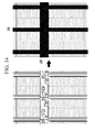
- the first black matrix 220 (which include portions extending in the vertical direction) and the second black matrix 225 (which include portions extending in the horizontal direction) may form a lattice structure having openings.
- a substantial portion of the pixel electrode 192, a substantial portion of the color filter 230, and a substantial portion of the liquid crystal layer 3 may be positioned at one or more corresponding openings.
- a lower polarizer (not illustrated) may be positioned below the insulation substrate 110, and an upper polarizer may be positioned above the upper insulating layer 313.
- Each of the polarizers may include a polarized element for generating polarization and a tri-acetyl-cellulose (TAC) layer for ensuring durability.
- TAC tri-acetyl-cellulose
- directions in transmissive axes of the upper polarizer and the lower polarizer may be vertical or parallel to each other.
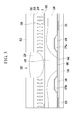
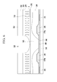
- a process for forming the microcavity 305 and for injecting and capping the liquid crystal layer 3 is described with reference to FIGS. 4 to 6 .
- FIGS. 4 to 6 are diagrams sequentially illustrating a manufacturing method of the liquid crystal display of FIG. 1 according to one or more embodiments of the present invention.
- FIG. 4 illustrates that the liquid crystal injection hole 335 is formed to expose the microcavity 305. Steps preceding the formation of the liquid crystal injection hole 335 are described below with reference to FIGS. 1 to 3 .
- the gate line 121 and the storage voltage line 131 are formed on the insulation substrate 110 made of transparent glass, transparent plastic, or a different transparent substrate material.
- the gate line 121 and the storage voltage line 131 may be substantially simultaneously formed of the same material using the same mask.
- the gate line 121 includes a first gate electrode 124a, a second gate electrode 124b, and a third gate electrode 124c.
- the storage voltage line 131 includes storage electrodes 135a and 135b and a protrusion 134 protruding in the gate line 121 direction.
- the storage electrodes 135a and 135b have a structure surrounding a first subpixel electrode 192h and a second subpixel electrode 1921 of a front pixel.
- the gate line 121 and the storage voltage line 131 are electrically insulated from each other.
- the storage voltage may have a constant voltage level or may have a swing (or variable) voltage level.
- a gate insulating layer 140 covering the gate line 121 and the storage voltage line 131 is formed on the gate line 121 and the storage voltage line 131.
- the semiconductors 151, 154, and 155, the data line 171, the source electrodes 173a, 173b, and 173c, and the drain electrodes 175a, 175b, and 175c are formed on the gate insulating layer 140.
- the semiconductors 151, 154, and 155, the data line 171, and the source electrodes and drain electrodes may be formed by separate processes or substantially simultaneously formed using one mask.
- materials for forming the semiconductors and material for forming the data line, the source electrodes, and the drain electrodes are sequentially laminated. Thereafter, two patterns are substantially simultaneously formed through one process of exposure, developing, and etching using one mask (e.g., a slit mask or a transflective mask).
- one mask e.g., a slit mask or a transflective mask.
- a plurality of ohmic contacts may be formed on the semiconductors 151, 154, and 155 and between the data line 171 and the source electrodes and/or the drain electrodes.
- the first passivation layer 180 is formed all over the data conductors 171, 173a, 173b, 173c, 175a, 175b, and 175c and the exposed semiconductor 154 portion.
- the first passivation layer 180 may contain an inorganic insulator, such as at least one of silicon nitride (SiNx) and silicon oxide (SiOx), or an organic insulator.
- the color filter 230 and the first black matrix 220 are formed on the first passivation layer 180.
- the color filter 230 is formed before the first black matrix 220 is formed.
- the color filter 230 for each color may be formed by a separate process. Portions of the color filter 230 that correspond to the positions of the contact holes 186a, 186b, and 186c may be removed during etching of the color filter 230.
- the first black matrix 220 is formed on the color filter 230 and is formed of a non-transmissive material for blocking light.
- the first black matrix 220 may extend in a vertical direction and may overlap the data line 171 without overlapping the transistor formation region.
- the second passivation layer 185 is formed all over the color filter 230 and the black matrix 220.
- the second passivation layer 185 may contain an inorganic insulator, such as at least one of silicon nitride (SiNx) and silicon oxide (SiOx), or an organic insulator.
- a first contact hole 186a and a second contact hole 186b exposing the first drain electrode 175a and the extension 175b' of the second drain electrode 175b, respectively, are formed in (and/or are formed through) the color filter 230, the black matrix 220, and the passivation layers 180 and 185. Further, in (and/or through) the color filter 230, the black matrix 220, and the passivation layers 180 and 185, the third contact hole 186c exposing the protrusion 134 of the storage voltage line 131 and the extension 175c' of the third drain electrode 175c is formed.
- the pixel electrode 192 including the first subpixel electrode 192h and the second subpixel electrode 1921 is formed on the second passivation layer 185.
- the pixel electrode 192 may be made of a transparent conductive material, such as ITO or IZO.
- the first subpixel electrode 192h and the second subpixel electrode 1921 are physically and electrically connected with the first drain electrode 175a and the second drain electrode 175b through the contact holes 186a and 186b, respectively.
- the connecting member 194 that electrically connects the extension 175c' of the third drain electrode 175c and the protrusion 134 of the storage voltage line 131 through the third contact hole 186c is formed.
- a part of the data voltage applied to the second drain electrode 175b is divided through the third source electrode 173c, and a magnitude of the voltage applied to the second subpixel electrode 1921 may be smaller than a magnitude of the voltage applied to the first subpixel electrode 192h.
- the sacrificial layer 300 (illustrated in FIG. 4 ) is formed.
- the sacrificial layer 300 may be made of an organic material, such as a photoresist material. The organic material is exposed, developed, and etched using a mask after the organic material has been laminated on the second passivation layer 185 and the pixel electrode 192, to form the sacrificial layer 300.
- the sacrificial layer 300 may have an opening above the data line 171 such that the sacrificial layer 300 may not substantially overlap the data line.
- the sacrificial layer 300 may extend in the data line 171 direction. At the opening, the sacrificial layer 300 may have a tapered side wall analogous to the tapered side wall of the liquid crystal layer 3 illustrated in FIG. 2 .
- the common electrode 270 and the lower insulating layer 311 are sequentially formed on the sacrificial layer 300, the sidewalls of the opening of the sacrificial layer 300, and the exposed portion of the second passivation layer 185 that is exposed at the opening.
- a transparent conductive material such as ITO or IZO
- SiNx silicon nitride
- the roof layer 312 is formed on the lower insulating layer 311.
- the roof layer 312 may contain an organic material.
- the roof layer 312 may not be formed in the transistor formation region, which may correspond to the location for the liquid crystal injection hole 335, i.e., the roof layer 312 may have an opening at the transistor formation region.
- the lower insulating layer 311 is exposed by the roof layer 312 opening in the transistor formation region.
- the roof layer 312 is exposed and developed using a mask after a roof layer material (containing an organic material) has been laminated in the entire panel area and after a portion of the roof layer material corresponding to the transistor formation region has been removed.
- the sacrificial layer 300, the common electrode 270, and the lower insulating layer 311, but not the roof layer 312, are formed in the transistor formation region, and the sacrificial layer 300, the common electrode 270, the lower insulating layer 311, and the roof layer 312 are laminated in regions of the panel other than the transistor formation region.
- the upper insulating layer 313 is formed on the roof layer 312 and formed on the exposed lower insulating layer 311 in the transistor formation region.
- a photoresist pattern PR having an opening in the transistor formation region is formed on the upper insulating layer 313.
- the upper insulating layer 313, the lower insulating layer 311, and the common electrode 270 are etched using the photoresist pattern PR as a mask.
- the sacrificial layer 300 is exposed by the liquid crystal injection hole 335, as illustrated in FIG. 4 .
- the etching process for forming the liquid crystal injection hole 335 may be performed through dry etching and/ or wet etching.
- the sacrificial layer 300 exposed through the liquid crystal injection hole 335 is removed to form the microcavity 305.
- the sacrificial layer 300 is made of the photoresist material used for forming the photoresist pattern PR, and the process of removing the photoresist pattern PR formed on the upper insulating layer 313 may be performed when removing the sacrificial layer 300. That is, the photoresist pattern PR formed on the upper insulating layer 313 and the sacrificial layer 300 may be substantially simultaneously wet-etched and removed by immersing the structure illustrated in FIG. 4 in an etchant (for example, a photo resist stripper).
- an etchant for example, a photo resist stripper
- the manufacturing process may be substantially shortened and simplified.
- the sacrificial layer 300 may be formed of a material that is different from the material of the photoresist pattern PR, and two separate process steps may be performed for removing the sacrificial layer 300 and the photo resist pattern PR.
- the sacrificial layer 300 may be removed through dry etching, alternative or in addition to wet etching.
- an alignment layer (not illustrated) and/or the liquid crystal layer 3 (illustrated in FIG. 6 ) are injected in the microcavity 305 using capillary force.
- the microcavity 305 and the liquid crystal injection hole 335 are connected without obstacles.
- the black matrix to be positioned in the transistor formation region is not formed before the injection of the liquid crystal, and thus the liquid crystal injection may be substantially easy and efficient.
- the second black matrix 225 is formed in the liquid crystal injection hole 335 to prevent transmission of light in the transistor formation region and to cap (and/or seal) the liquid crystal layer 3 so as to prevent leakage of liquid crystal of the liquid crystal layer 3.
- the second black matrix 225 is formed of a non-transmissive material in the transistor formation region and in the liquid crystal injection hole 335.
- the second black matrix 225 is formed by injecting the non-transmissive material using an inkjet method. At least a portion of the second black matrix 225 is positioned in the liquid crystal injection hole 335. According to one or more embodiments, a part of the second black matrix 225 may be positioned outside the liquid crystal injection hole 335. Since the second black matrix 225 covers the transistor formation region, light passing through the transistor formation region is blocked, and thus the transistor formation region is not recognized by a viewer of the liquid crystal display.
- the second black matrix 225 may also seal the liquid crystal layer 3 so as to prevent the liquid crystal layer 3 from leaking through the liquid crystal injection hole 335 after the liquid crystal layer 3 has been injected through the liquid crystal injection hole 335 into the microcavity 305.
- the second black matrix 225 extends in a horizontal direction along the transistor formation region.
- the first black matrix 220 (which include portions extending in the vertical direction) and the second black matrix 225 (which include portions extending in the horizontal direction) may form a lattice structure having openings.
- a substantial portion of the pixel electrode 192, a substantial portion of the color filter 230, and a substantial portion of the liquid crystal layer 3 may be positioned at one or more corresponding openings.
- the lower insulating layer 311 and the upper insulating layer 313 may not be required.
- a lower polarizer (not illustrated) may be disposed below the insulation substrate 110, and an upper polarizer may be disposed above the upper insulating layer 313.
- Each of the polarizers may include a polarized element for generating polarization and a tri-acetyl-cellulose (TAC) layer for ensuring durability.
- TAC tri-acetyl-cellulose
- directions in transmissive axes of the upper polarizer and the lower polarizer may be vertical or parallel to each other.
- the second black matrix 225 is formed after the liquid crystal layer 3 has been injected into the microcavity 305. Therefore, the second black matrix 225 may not block the injection of liquid crystal for forming the liquid crystal layer 3.
- the liquid crystal layer 3 may be substantially easily and efficiently formed.
- the second black matrix 225 seals the liquid crystal layer 3 to serve as a capping layer so as to prevent the liquid crystal layer 3 from leaking through the liquid crystal injection hole 335.
- an additional or alternative capping layer may be formed, as illustrated in FIGS. 7 to 11 .
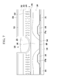
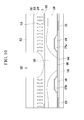
- FIG. 7 is a cross-sectional view illustrating a liquid crystal display, e.g., the liquid crystal display of FIG. 1 , according to one or more embodiments of the present invention.
- FIG. 7 may be a cross-sectional view taken line III-III indicated in FIG. 1 .
- the liquid crystal display may include a capping layer 350.
- a gate line 121 and a storage voltage line 131 are formed on an insulation substrate 110 made of transparent glass, transparent plastic, or a different transparent substrate material.
- the gate line 121 includes a first gate electrode 124a, a second gate electrode 124b, and a third gate electrode 124c.
- the storage voltage line 131 includes storage electrodes 135a and 135b and a protrusion 134 protruding in the gate line 121 direction (i.e., the horizontal direction).
- the storage electrodes 135a and 135b may form a structure that surrounds a first subpixel electrode 192h and a second subpixel electrode 1921 of a front pixel.
- a horizontal portion of the storage electrode 135b may be one wiring which is not separated from the horizontal portion of the front pixel.
- a gate insulating layer 140 is formed on the gate line 121 and the storage voltage line 131.
- a semiconductor 151 positioned below a data line 171, portions of a semiconductor 155 positioned below one or more drain electrodes (e.g., a drain electrode 175b), and a semiconductor 154 positioned at a channel part of a thin film transistor are formed on the gate insulating layer 140.
- a plurality of ohmic contacts may be respectively formed on the semiconductors 151, 154, and 155 and between the data line 171 and the one or more source electrodes and/or the one or more drain electrodes, is the ohmic contacts being omitted in the drawings.
- a set of data conductors that includes a plurality of data lines 171 including a first source electrode 173a and a second source electrode 173b, a first drain electrode 175a, a second drain electrode 175b, a third source electrode 173c, and a third drain electrode 175c is formed.
- the first gate electrode 124a, the first source electrode 173a, and the first drain electrode 175a form a first thin film transistor together with the semiconductor 154, and a channel of the thin film transistor is formed at the semiconductor portion 154 between the first source electrode 173a and the first drain electrode 175a.
- the second gate electrode 124b, the second source electrode 173b, and the second drain electrode 175b form a second thin film transistor together with the semiconductor 154, and a channel of the thin film transistor is formed at the semiconductor portion 154 between the second source electrode 173b and the second drain electrode 175b.
- the third gate electrode 124c, the third source electrode 173c, and the third drain electrode 175c form a third thin film transistor together with the semiconductor 154, and a channel of the thin film transistor is formed at the semiconductor portion 154 between the third source electrode 173c and the third drain electrode 175c.
- the data line 171 of may have a structure with a narrow width in a thin film transistor formation region around (or near) an extension 175c' of the third drain electrode 175c. This structure is for keeping a distance from the adjacent wiring and reducing signal interference. In one or more embodiments, the structure may not be required.
- a first passivation layer 180 is formed on the data conductors 171, 173c, 175a, 175b, and 175c and the exposed semiconductor 154 portion.
- the first passivation layer 180 may include an inorganic insulator, such as at least one of silicon nitride (SiNx) and silicon oxide (SiOx), or an organic insulator.
- a color filter 230 is formed on the first passivation layer 180.
- the color filter 230 having the same color is formed in adjacent pixels in a vertical direction (i.e., the data line direction).
- Adjacent pixels in a horizontal direction i.e., the gate line direction
- Each of the color filters 230 and 230' may display one color of a set of primary colors such as three primary colors of red, green, and blue.
- each of the color filters 230 and 230' may display one color of cyan, magenta, yellow, and white-based colors.
- a first black matrix 220 i.e., a black matrix portion overlapping and/or covering a data line, is formed on the color filters 230 and 230' and overlaps at least a portion of each of the color filters 230 and 230'.
- the first black matrix 220 is made of a non-transmissive material for blocking light.
- the first black matrix 220 is formed based on a region where the data line 171 is formed to extend in a vertical direction and is not formed in a 'transistor formation region', a region where the gate line 121, the storage voltage line 131, and one or more thin film transistors are formed, such that the first black matrix 220 may not overlap the gate line 121, the storage voltage line 131, or the one or more thin film transistors.
- a black matrix 225 may overlap the transistor formation region and may block light in the transistor formation region.
- the second black matrix 225 i.e., a black matrix disposed in a liquid crystal injection hole 335, may be formed after liquid crystal molecules have been injected in a microcavity (e.g., microcavity 305 illustrated in FIG. 5 ). This will be described below.
- a second passivation layer 185 may cover the color filter 230 and the black matrix 220 and may be formed on the color filter 230 and the black matrix 220.
- the second passivation layer 185 may contain an inorganic insulator, such as at least one of silicon nitride (SiNx) and silicon oxide (SiOx), or an organic insulator. As illustrated in cross-sectional views of FIGS.
- the second passivation layer 185 may reduce or compensate the thickness difference and/or the thickness variation; the second passivation layer 185 may server as a planarization layer disposed over the color filter 230 and the black matrix 220.
- a first contact hole 186a and a second contact hole 186b which expose the first drain electrode 175a and an extension 175b' of the second drain electrode 175b, respectively, are formed in (and/ or are formed through) one or more of the color filter 230, the first black matrix 220, and the passivation layers 180 and 185.
- a third contact hole 186c, which exposes a protrusion 134 of the storage voltage line 131 and the extension 175c' of the third drain electrode 175c is formed in (and/or is formed through) on or more of the color filter 230, the first black matrix 220, and the passivation layers 180 and 185.
- the contact holes 186a, 186b, and 186c are formed in (and/ or are formed through) the first black matrix 220 and the color filter 230, even if etching the first black matrix 220 and the color filter 230 may be more difficult than etching the passivation layers 180 and 185 because of material properties.
- the material used for forming the first black matrix 220 or the color filter 230 may not be formed at positions corresponding to the contact holes 186a, 186b, and 186c before etching of the black matrix 220 or the color filter 230.
- the color filter 230 and the passivation layers 180 and 185 may be etched, and a position of the first black matrix 220 may be changed, in order to form the contact holes 186a, 186b, and 186c.
- a pixel electrode 192 including the first subpixel electrode 192h and the second subpixel electrode 1921 is formed on the second passivation layer 185.
- the pixel electrode 192 may be made of a transparent conductive material such as ITO or IZO.
- the first subpixel electrode 192h and the second subpixel electrode 1921 are adjacent to each other in a column direction.
- Each of the first subpixel electrode 192h and the second subpixel electrode 1921 may have an overall quadrangular shape, and include a cross stem configured by a horizontal stem and a vertical stem crossing the horizontal stem.
- Each of the first subpixel electrode 192h and the second subpixel electrode 1921 may be divided into four subregions by the horizontal stem and the vertical stem, and each subregion may include a plurality of minute branches.
- the minute branches of the first subpixel electrode 192h and the second subpixel electrode 1921 form an angle in a range of approximately 40 to 45 degrees with the gate line 121 or the horizontal stem.
- the minute branches of two adjacent subregions may be perpendicular to each other.
- a width of the minute branch may be gradually increased. Distances between the minute branches may be different from each other.
- the first subpixel electrode 192h and the second subpixel electrode 1921 are physically and electrically connected with the first drain electrode 175a and the second drain electrode 175b through the contact holes 186a and 186b and receive data voltage from the first drain electrode 175a and the second drain electrode 175b.
- a connecting member 194 electrically connects the extension 175c' of the third drain electrode 175c and the protrusion 134 of the storage voltage line 131 through the third contact hole 186c.
- a part of the data voltage applied to the second drain electrode 175b is divided through the third source electrode 173c, and a magnitude of the voltage applied to the second subpixel electrode 1921 may be smaller than a magnitude of the voltage applied to the first subpixel electrode 192h.
- An area of the second subpixel electrode 1921 may be in a range of 1 to 2 times an area of the first subpixel electrode 192h.
- An opening for collecting gas discharged from the color filter 230 and a cover for covering the opening may be formed in the second passivation layer 185.
- the cover may be formed of the same material as the pixel electrode 192.
- the opening and the cover may prevent gas discharged from the color filter 230 from being transferred to other elements. In one or more embodiments, the opening and the cover may not be required.
- a microcavity 305 is positioned on the second passivation layer 185 and the pixel electrode 192 (and is positioned between the second passivation layer 185 and a common electrode 270), and the liquid crystal layer 3 is formed in the microcavity.
- An alignment layer (not illustrated) may be formed between the second passivation layer 185 and the liquid crystal layer 3 in order to align the liquid crystal molecules injected in the microcavity 305.
- the alignment layer may contain at least one of polyamic acid, polysiloxane, and polyimide, which are generally used in a liquid crystal alignment layer.
- the liquid crystal layer 3 is formed in the microcavity 305 (and on the alignment layer).
- the liquid crystal molecules 310 are initially aligned by the alignment layer and the alignment direction is changed according to the applied electric field.
- a height of the liquid crystal layer 3 corresponds to a height of the microcavity 305.
- a thickness of the liquid crystal layer 3 may be in a range of 2.0 ⁇ m to 3.6 ⁇ m.
- Liquid crystal material for forming the liquid crystal layer 3 may be injected into the microcavity 305 using capillary force in a liquid crystal injection hole 335.
- the alignment layer may be formed capillary force.
- the common electrode 270 is positioned above the microcavity 305 and the liquid crystal layer 3 with the microcavity 305 and the liquid crystal layer 3 being disposed between the common electrode 270 and the second passivation layer 185.
- the common electrode 270 may have a curved structure including a protrusion portion (illustrated in FIG. 2 ) that is disposed above a data line 171 and protrudes (and is convex) toward the data line 171. At least a portion of the first black matrix 220 may be disposed between the protrusion portion and the data line 171. The protrusion portion may directly contact the second passivation layer 185.
- a portion of the roof material 312 and a portion of the lower insulating layer 311 may be disposed inside a recess structure of the protrusion portion.
- the common electrode 270 is not formed in the liquid crystal injection hole 335 portion (which corresponds to the transistor formation region); the liquid crystal injection hole 335 may be disposed between two portions of the common electrode 270, as illustrated in FIG. 3 .
- the common electrode 270 may extend in a gate line direction (i.e., the horizontal direction).
- the common electrode 270 is made of a transparent conductive material, such as ITO or IZO, and serves to generate an electric field together with the pixel electrode 192 to control an alignment direction of the liquid crystal molecules.
- a lower insulating layer 311 is positioned on the common electrode 270.
- the lower insulating layer 311 may contain an inorganic insulating material such as silicon nitride (SiNx).
- a roof layer 312 is formed on the lower insulating layer 311.
- the roof layer 312 may serve to support a space (microcavity 305) to be formed between the pixel electrode 192 and the common electrode 270.
- the roof layer 312 according to one or more embodiments serves to support the microcavity 305 above the common electrode 270 at a predetermined thickness.
- the upper insulating layer 313 is formed on the roof layer 312.
- the upper insulating layer 313 may contain an inorganic insulating material, such as silicon nitride (SiNx).
- the liquid crystal injection hole 335 may be formed through the lower insulating layer 311, the roof layer 312, and the upper insulating layer 313 in the transistor formation region, wherein a liquid crystal may be injected through the liquid crystal injection hole 335 into the microcavity 305.
- the liquid crystal injection hole 335 may be used for removing the sacrificial layer 300 of FIG. 4 in the process of forming the microcavity 305..
- the lower insulating layer 311 and the upper insulating layer 313 may be laminated with portions disposed in the transistor formation region corresponding to a position for forming the liquid crystal injection hole 335.
- the roof layer 312 may not be formed in the transistor formation region; therefore, the liquid crystal injection hole 335 may be formed by removing portions of the lower insulating layer 311 and upper insulating layer 313 in the transistor formation region without removing portions of the roof layer 312.
- the sacrificial layer 300 may be exposed through the liquid crystal injection hole 335 after a portion of the common electrode 270 that is positioned in the transistor formation region has been removed.
- the roof layer 312, the upper insulating layer 313, and the lower insulating layer 311 are etched in the transistor formation region to form the liquid crystal injection hole 335.
- the lower insulating layer 311 and the upper insulating layer 313 may be omitted.
- a capping layer 350 is formed on the liquid crystal injection hole 335 and the upper insulating layer 313.
- the capping layer 350 is made of a transparent material and may contain an organic insulating material or an inorganic insulating material, such as silicon nitride (SiNx).
- the capping layer 350 as illustrated in FIG. 7 , may be formed throughout the entire display panel. In one or more embodiments, the capping layer 350 may be formed only near the liquid crystal injection hole 335.
- the capping layer 350 serves to seal the liquid crystal injection hole 335 after the liquid crystal material of the liquid crystal layer 3 has been injected into the microcavity 305 so as to prevent the liquid crystal layer 3 from leaking through the liquid crystal injection hole 335.
- a portion of the liquid crystal layer 3 may be disposed between the second passivation layer 185 and the capping layer 350.
- the capping layer 350 may directly contact the second passivation layer 185 and thus may separate a first portion of the liquid crystal layer 3 from a second portion of the liquid crystal layer 3.
- the second black matrix 225 is formed on the capping layer 350, formed in the transistor formation region, formed in the liquid crystal injection hole 335. At least a portion of the capping layer 350 may be disposed between the second black matrix 225 and the second passivation layer 185 and may be disposed between the second black matrix 225 and a portion of the liquid crystal layer 3. At least a portion of the capping layer 350 (e.g., a portion that is substantially perpendicular to the substrate 110) may be disposed between the second black matrix 225 and at least a portion of one or more of the upper insulating layer 313, the roof layer 312, the lower insulating layer 311, the common electrode 270, and the liquid crystal layer 3.
- the second black matrix 225 is formed by injecting the material using an inkjet method. In one or more embodiments, at least a portion of the second black matrix 225 is positioned inside the liquid crystal injection hole 335. According to one or more embodiments, a part of the second black matrix 225 may be positioned outside the liquid crystal injection hole 335.
- the second black matrix 225 is formed of a non-transmissive material. Since the second black matrix 225 covers the transistor formation region, light passing through the transistor formation region is blocked, and thus the transistor formation region is not recognized by a viewer of the liquid crystal display. The second black matrix 225 extends in a horizontal direction along the transistor formation region.
- the first black matrix 220 (which include portions extending in the vertical direction) and the second black matrix 225 (which include portions extending in the horizontal direction) may form a lattice structure having openings.
- a substantial portion of the pixel electrode 192, a substantial portion of the color filter 230, and a substantial portion of the liquid crystal layer 3 may be positioned at one or more corresponding openings.
- a lower polarizer (not illustrated) may be positioned below the insulation substrate 110, and an upper polarizer may be positioned above the upper insulating layer 313.
- Each of the polarizers may include a polarized element for generating polarization and a tri-acetyl-cellulose (TAC) layer for ensuring durability.
- TAC tri-acetyl-cellulose
- directions in transmissive axes of the upper polarizer and the lower polarizer may be vertical or parallel to each other.
- a process for forming the microcavity 305 and for injecting and capping the liquid crystal layer 3 is described with reference to FIGS. 8 to 11 .
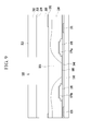
- FIGS. 8 to 11 are diagrams sequentially illustrating a manufacturing method of the liquid crystal display of FIGS. 1 and 7 according to one or more embodiments of the present invention.
- FIG. 8 illustrates that the liquid crystal injection hole 335 is formed to expose the microcavity 305. Steps preceding the formation of the liquid crystal injection hole 335 are described below with reference to at least some of FIGS. 1 to 7 .
- the gate line 121 and the storage voltage line 131 are formed on the insulation substrate 110 made of transparent glass, transparent plastic, or a different transparent substrate material.
- the gate line 121 and the storage voltage line 131 may be substantially simultaneously formed of the same material using the same mask.
- the gate line 121 includes a first gate electrode 124a, a second gate electrode 124b, and a third gate electrode 124c.
- the storage voltage line 131 includes storage electrodes 135a and 135b and a protrusion 134 protruding in the gate line 121 direction.
- the storage electrodes 135a and 135b have a structure surrounding a first subpixel electrode 192h and a second subpixel electrode 1921 of a front pixel.
- the gate line 121 and the storage voltage line 131 are electrically insulated from each other.
- the storage voltage may have a constant voltage level or may have a swing (or variable) voltage level.
- a gate insulating layer 140 covering the gate line 121 and the storage voltage line 131 is formed on the gate line 121 and the storage voltage line 131.
- the semiconductors 151, 154, and 155, the data line 171, the source electrodes 173a, 173b, and 173c, and the drain electrodes 175a, 175b, and 175c are formed on the gate insulating layer 140.
- the semiconductors 151, 154, and 155, the data line 171, and the source electrodes and drain electrodes may be formed by separate processes or substantially simultaneously formed using one mask.
- materials for forming the semiconductors and material for forming the data line, the source electrodes, and the drain electrodes are sequentially laminated. Thereafter, two patterns are substantially simultaneously formed through one process of exposure, developing, and etching using one mask (e.g., a slit mask or a transflective mask).
- one mask e.g., a slit mask or a transflective mask.
- a plurality of ohmic contacts may be formed on the semiconductors 151, 154, and 155 and between the data line 171 and the source electrodes and/or the drain electrodes.
- the first passivation layer 180 is formed all over the data conductors 171, 173a, 173b, 173c, 175a, 175b, and 175c and the exposed semiconductor 154 portion.
- the first passivation layer 180 may contain an inorganic insulator, such as at least one of silicon nitride (SiNx) and silicon oxide (SiOx), or an organic insulator.
- the color filter 230 and the first black matrix 220 are formed on the first passivation layer 180.
- the color filter 230 is formed before the first black matrix 220 is formed.
- the color filter 230 for each color may be formed by a separate process. Portions of the color filter 230 that correspond to the positions of the contact holes 186a, 186b, and 186c may be removed during etching of the color filter 230.
- the first black matrix 220 is formed on the color filter 230 and is formed of a non-transmissive material for blocking light.
- the first black matrix 220 may extend in a vertical direction and may overlap the data line 171 without overlapping the transistor formation region.
- the second passivation layer 185 is formed all over the color filter 230 and the black matrix 220.
- the second passivation layer 185 may contain an inorganic insulator, such as at least one of silicon nitride (SiNx) and silicon oxide (SiOx), or an organic insulator.
- a first contact hole 186a and a second contact hole 186b exposing the first drain electrode 175a and the extension 175b' of the second drain electrode 175b, respectively are formed in (and/ or are formed through) the color filter 230, the black matrix 220, and the passivation layers 180 and 185. Further, in (and/or through) the color filter 230, the black matrix 220, and the passivation layers 180 and 185, the third contact hole 186c exposing the protrusion 134 of the storage voltage line 131 and the extension 175c' of the third drain electrode 175c is formed.
- the pixel electrode 192 including the first subpixel electrode 192h and the second subpixel electrode 1921 is formed on the second passivation layer 185.
- the pixel electrode 192 may be made of a transparent conductive material, such as ITO or IZO.
- the first subpixel electrode 192h and the second subpixel electrode 1921 are physically and electrically connected with the first drain electrode 175a and the second drain electrode 175b through the contact holes 186a and 186b, respectively.
- the connecting member 194 that electrically connects the extension 175c' of the third drain electrode 175c and the protrusion 134 of the storage voltage line 131 through the third contact hole 186c is formed.
- a part of the data voltage applied to the second drain electrode 175b is divided through the third source electrode 173c, and a magnitude of the voltage applied to the second subpixel electrode 1921 may be smaller than a magnitude of the voltage applied to the first subpixel electrode 192h.
- the sacrificial layer 300 (illustrated in FIG. 8 ) is formed.
- the sacrificial layer 300 may be made of an organic material, such as a photoresist material. The organic material is exposed, developed, and etched using a mask after the organic material has been laminated on the second passivation layer 185 and the pixel electrode 192, to form the sacrificial layer 300.
- the sacrificial layer 300 may have an opening above the data line 171 such that the sacrificial layer 300 may not substantially overlap the data line.
- the sacrificial layer 300 may extend in the data line 171 direction. At the opening, the sacrificial layer 300 may have a tapered side wall analogous to the tapered side wall of the liquid crystal layer 3 illustrated in FIG. 2 .
- the common electrode 270 and the lower insulating layer 311 are sequentially formed on the sacrificial layer 300, the sidewalls of the opening of the sacrificial layer 300, and the exposed portion of the second passivation layer 185 that is exposed at the opening.
- a transparent conductive material such as ITO or IZO
- SiNx silicon nitride
- the roof layer 312 is formed on the lower insulating layer 311.
- the roof layer 312 may contain an organic material.
- the roof layer 312 may not be formed in the transistor formation region, which may correspond to the location for the liquid crystal injection hole 335, i.e., the roof layer 312 may have an opening at the transistor formation region.
- the lower insulating layer 311 is exposed by the roof layer 312 opening in the transistor formation region.
- the roof layer 312 is exposed and developed using a mask after a roof layer material (containing an organic material) has been laminated in the entire panel area and after a portion of the roof layer material corresponding to the transistor formation region has been removed.
- the sacrificial layer 300, the common electrode 270, and the lower insulating layer 311, but not the roof layer 312, are formed in the transistor formation region, and the sacrificial layer 300, the common electrode 270, the lower insulating layer 311, and the roof layer 312 are laminated in regions of the panel other than the transistor formation region.
- the upper insulating layer 313 is formed on the roof layer 312 and formed on the exposed lower insulating layer 311 in the transistor formation region.
- a photoresist pattern PR having an opening in the transistor formation region is formed on the upper insulating layer 313.
- the upper insulating layer 313, the lower insulating layer 311, and the common electrode 270 are etched using the photoresist pattern PR as a mask.
- the sacrificial layer 300 is exposed by the liquid crystal injection hole 335, as illustrated in FIG. 8 .
- the etching process for forming the liquid crystal injection hole 335 may be performed through dry etching and/ or wet etching.
- the sacrificial layer 300 exposed through the liquid crystal injection hole 335 is removed to form the microcavity 305.
- the sacrificial layer 300 is made of the photoresist material used for forming the photoresist pattern PR, and the process of removing the photoresist pattern PR formed on the upper insulating layer 313 may be performed when removing the sacrificial layer 300. That is, the photoresist pattern PR formed on the upper insulating layer 313 and the sacrificial layer 300 may be substantially simultaneously wet-etched and removed by immersing the structure illustrated in FIG. 4 in an etchant (for example, a photo resist stripper).
- an etchant for example, a photo resist stripper
- the manufacturing process may be substantially shortened and simplified.
- the sacrificial layer 300 may be formed of a material that is different from the material of the photoresist pattern PR, and two separate process steps may be performed for removing the sacrificial layer 300 and the photo resist pattern PR.
- the sacrificial layer 300 may be removed through dry etching, alternative or in addition to wet etching.
- an alignment layer (not illustrated) and/or the liquid crystal layer 3 (illustrated in FIG. 10 ) are injected in the microcavity 305 using capillary force.
- an alignment layer (not illustrated) and/or the liquid crystal layer 3 (illustrated in FIG. 10 ) are injected in the microcavity 305 using capillary force.
- the microcavity 305 and the liquid crystal injection hole 335 are connected without obstacles.
- the black matrix to be positioned in the transistor formation region is not formed before the injection of the liquid crystal, and thus the liquid crystal injection may be substantially easy and efficient.
- a capping process for preventing the liquid crystal layer 3 from flowing out through the liquid crystal injection hole 335 is performed.
- the capping layer 350 is formed to seal the liquid crystal injection hole 335 such that leakage of the liquid crystal layer 3 may be prevented.
- the capping layer 350 is formed in the liquid crystal injection hole 335 and is formed on the upper insulating layer 313.
- the capping layer 350 is made of a transparent material and may contain an organic insulating material or an inorganic insulating material, such as silicon nitride (SiNx).
- the capping layer 350 is formed throughout the entire display panel. According to one or more embodiments, the capping layer 350 may be formed only near the liquid crystal injection hole 335.
- the capping layer 350 serves to seal the liquid crystal injection hole 335 after the liquid crystal material of the liquid crystal layer 3 has been injected into the microcavity 305 so as to prevent the liquid crystal layer 3 from leaking through the liquid crystal injection hole 335.
- the second black matrix 225 which is formed of a non-transmissive material, may be formed on the capping layer 350, formed in the transistor formation region, and formed in the liquid crystal injection hole 335.
- the second black matrix 225 is formed by injecting the material using an inkjet method.
- at least a portion of the second black matrix 225 is positioned inside the liquid crystal injection hole 335.
- a part of the second black matrix 225 may be positioned outside the liquid crystal injection hole 335. Since the second black matrix 225 covers the transistor formation region, light passing through the transistor formation region is blocked and thus the transistor formation region is not recognized by a viewer of the liquid crystal display.
- the second black matrix 225 extends in a horizontal direction along the transistor formation region.
- the first black matrix 220 (which include portions extending in the vertical direction) and the second black matrix 225 (which include portions extending in the horizontal direction) may form a lattice structure having openings.
- a substantial portion of the pixel electrode 192, a substantial portion of the color filter 230, and a substantial portion of the liquid crystal layer 3 may be positioned at one or more corresponding openings.
- the lower insulating layer 311 and the upper insulating layer 313 may not be required.
- a lower polarizer (not illustrated) may be disposed below the insulation substrate 110, and an upper polarizer may be disposed above the upper insulating layer 313.
- Each of the polarizers may include a polarized element for generating polarization and a tri-acetyl-cellulose (TAC) layer for ensuring durability.
- TAC tri-acetyl-cellulose
- directions in transmissive axes of the upper polarizer and the lower polarizer may be vertical or parallel to each other.
- the capping layer 350 and the second black matrix 225 may be formed after the liquid crystal layer 3 has been injected into the microcavity 305. Therefore, the second black matrix 225 may not block the injection of liquid crystal for forming the liquid crystal layer 3.
- the liquid crystal layer 3 may be substantially easily and efficiently formed.
- the liquid crystal layer 3 may not leak through the liquid crystal injection hole 335, which is sealed by at least the capping layer 350.
- the material of the second black matrix 225 may cause contamination and/or deterioration to the liquid crystal layer 3 during or after a manufacturing process of the second black matrix 225, and the capping layer 350, which is disposed between the liquid crystal layer 3 and the second black matrix 225 may prevent such contamination and/ or deterioration.
- the formation process of liquid crystal layer 3 may be performed between the formation process of the first black matrix 220 and the formation process of the second black matrix 225, such that the formation of the liquid crystal layer 3 may not be obstructed by the second black matrix 225.
- the first black matrix 220 and the second black matrix 225 may be formed in two separate processes and may be located at two different layers in the liquid crystal display.
- a first black matrix 220 and a second black matrix 225 may be substantially simultaneously formed in one process.
- FIGS. 12 and 13 are cross-sectional views illustrating a liquid crystal display, e.g., the liquid crystal display of FIG. 1 , according to one or more embodiments of the present invention
- FIG. 14 is a plan view illustrating positions of a first black matrix and a second black matrix in the liquid crystal display of FIGS. 12 and 13 .
- FIGS. 12 and 13 may be cross-sectional views taken along a cross-sectional line II-II indicated in FIG. 1 and a cross-sectional line III-III indicated in FIG. 1 , respectively.
- both the first black matrix 220 and the second black matrix 225 may be positioned at the upper side (i.e., a same side) with respect to the liquid crystal layer 3.
- the second black matrix 225 may be configured to seal the liquid crystal injection hole 335.
- an additional capping layer may be formed to seal the liquid crystal injection hole 335.
- gate line 121 and a storage voltage line 131 are formed on an insulation substrate 110 made of transparent glass, transparent plastic, or a different transparent substrate material.
- the gate line 121 includes a first gate electrode 124a, a second gate electrode 124b, and a third gate electrode 124c.
- the storage voltage line 131 includes storage electrodes 135a and 135b and a protrusion 134 protruding in the gate line 121 direction (i.e., the horizontal direction).
- the storage electrodes 135a and 135b may form a structure that surrounds a first subpixel electrode 192h and a second subpixel electrode 1921 of a front pixel.
- a horizontal portion of the storage electrode 135b may be one wiring which is not separated from the horizontal portion of the front pixel.
- a gate insulating layer 140 is formed on the gate line 121 and the storage voltage line 131.
- a semiconductor 151 positioned below a data line 171, portions of a semiconductor 155 positioned below one or more drain electrodes (e.g., a drain electrode 175b), and a semiconductor 154 positioned at a channel part of a thin film transistor are formed on the gate insulating layer 140.
- a plurality of ohmic contacts may be respectively formed on the semiconductors 151, 154, and 155 and between the data line 171 and the one or more source electrodes and/or the one or more drain electrodes, the ohmic contacts being omitted in the drawings.
- a set of data conductors that includes a plurality of data lines 171 including a first source electrode 173a and a second source electrode 173b, a first drain electrode 175a, a second drain electrode 175b, a third source electrode 173c, and a third drain electrode 175c is formed.
- the first gate electrode 124a, the first source electrode 173a, and the first drain electrode 175a form a first thin film transistor together with the semiconductor 154, and a channel of the thin film transistor is formed at the semiconductor portion 154 between the first source electrode 173a and the first drain electrode 175a.
- the second gate electrode 124b, the second source electrode 173b, and the second drain electrode 175b form a second thin film transistor together with the semiconductor 154, and a channel of the thin film transistor is formed at the semiconductor portion 154 between the second source electrode 173b and the second drain electrode 175b.
- the third gate electrode 124c, the third source electrode 173c, and the third drain electrode 175c form a third thin film transistor together with the semiconductor 154, and a channel of the thin film transistor is formed at the semiconductor portion 154 between the third source electrode 173c and the third drain electrode 175c.
- the data line 171 of may have a structure with a narrow width in a thin film transistor formation region near an extension 175c' of the third drain electrode 175c. This structure is for keeping a distance from the adjacent wiring and reducing signal interference. In one or more embodiments, the structure may not be required.
- a first passivation layer 180 is formed on the data conductors 171, 173c, 175a, 175b, and 175c and the exposed semiconductor 154 portion.
- the first passivation layer 180 may include an inorganic insulator, such as at least one of silicon nitride (SiNx) and silicon oxide (SiOx), or an organic insulator.
- a color filter 230 is formed on the first passivation layer 180.
- the color filter 230 having the same color is formed in adjacent pixels in a vertical direction (i.e., the data line direction).
- Adjacent pixels in a horizontal direction i.e., the gate line direction
- Each of the color filters 230 and 230' may display one color of a set of primary colors such as three primary colors of red, green, and blue.
- each of the color filters 230 and 230' may display one color of cyan, magenta, yellow, and white-based colors.
- a second passivation layer 185 may cover the color filter 230 and may be formed on the color filter 230.
- the second passivation layer 185 may contain an inorganic insulator, such as at least one of silicon nitride (SiNx) and silicon oxide (SiOx), or an organic insulator.
- SiNx silicon nitride
- SiOx silicon oxide
- the second passivation layer 185 may reduce or compensate the thickness difference and/or the thickness variation; the second passivation layer 185 may server as a planarization layer disposed over the color filter 230.
- a first contact hole 186a and a second contact hole 186b which expose the first drain electrode 175a and an extension 175b' of the second drain electrode 175b, respectively, are formed in (and/ or are formed through) one or more of the color filter 230 and the passivation layers 180 and 185.
- a third contact hole 186c which exposes a protrusion 134 of the storage voltage line 131 and the extension 175c' of the third drain electrode 175c is formed in (and/or is formed through) on or more of the color filter 230 and the passivation layers 180 and 185.
- the contact holes 186a, 186b, and 186c are formed in (and/or are formed through) the color filter 230, even if etching the color filter 230 may be more difficult than etching the passivation layers 180 and 185 because of material properties.
- the material used for forming the color filter 230 may be formed at position corresponding to the contact holes 186a, 186b, and 186c before etching the color filter 230.
- a pixel electrode 192 including the first subpixel electrode 192h and the second subpixel electrode 1921 is formed on the second passivation layer 185.
- the pixel electrode 192 may be made of a transparent conductive material, such as ITO or IZO.
- the first subpixel electrode 192h and the second subpixel electrode 1921 are adjacent to each other in a column direction.
- Each of the first subpixel electrode 192h and the second subpixel electrode 1921 may have an overall quadrangular shape, and may include a cross stem structure having a horizontal stem and a vertical stem crossing the horizontal stem.
- Each of the first subpixel electrode 192h and the second subpixel electrode 1921 may be divided into four subregions by the horizontal stem and the vertical stem, and each subregion may include a plurality of minute branches.
- the minute branches of the first subpixel electrode 192h and the second subpixel electrode 1921 form an angle of approximately in a range of 40 to 45 degrees with the gate line 121 or the horizontal stem.
- the minute branches of two adjacent subregions may be perpendicular to each other.
- a width of the minute branch may be gradually increased. Distances between the minute branches may be different from each other.
- the first subpixel electrode 192h and the second subpixel electrode 1921 are physically and electrically connected with the first drain electrode 175a and the second drain electrode 175b through the contact holes 186a and 186b and receive data voltage from the first drain electrode 175a and the second drain electrode 175b.
- a connecting member 194 electrically connects the extension 175c' of the third drain electrode 175c and the protrusion 134 of the storage voltage line 131 through the third contact hole 186c.
- a part of the data voltage applied to the second drain electrode 175b is divided through the third source electrode 173c, and a magnitude of the voltage applied to the second subpixel electrode 1921 may be smaller than a magnitude of the voltage applied to the first subpixel electrode 192h.
- An area of the second subpixel electrode 1921 may be in a range of 1 to 2 times an area of the first subpixel electrode 192h.
- An opening for collecting gas discharged from the color filter 230 and a cover for covering the opening may be formed in the second passivation layer 185.
- the cover may be formed of the same material as the pixel electrode 192.
- the opening and the cover may prevent gas discharged from the color filter 230 from being transferred to other elements. In one or more embodiments, the opening and the cover may not be required.
- a microcavity 305 is positioned on the second passivation layer 185 and the pixel electrode 192 (and is positioned between the second passivation layer 185 and a common electrode 270), and the liquid crystal layer 3 is formed in the microcavity.
- An alignment layer (not illustrated) may be formed between the second passivation layer 185 and the liquid crystal layer 3 in order to align the liquid crystal molecules injected in the microcavity 305.
- the alignment layer may contain at least one of polyamic acid, polysiloxane, and polyimide, which are generally used in a liquid crystal alignment layer.
- the liquid crystal layer 3 is formed in the microcavity 305 (and on the alignment layer).
- the liquid crystal molecules 310 are initially aligned by the alignment layer and the alignment direction is changed according to the applied electric field.
- a height of the liquid crystal layer 3 corresponds to a height of the microcavity 305.
- a thickness of the liquid crystal layer 3 may be in a range of 2.0 ⁇ m to 3.6 ⁇ m.
- the liquid crystal material for forming the liquid crystal layer 3 may be injected into the microcavity 305 using capillary force in a liquid crystal injection hole 335.
- the alignment layer may be formed using capillary force.
- the common electrode 270 is positioned above the microcavity 305 and the liquid crystal layer 3 with the microcavity 305 and the liquid crystal layer 3 being disposed between the common electrode 270 and the second passivation layer 185.
- the common electrode 270 may have a curved structure including a protrusion portion (illustrated in FIG. 2 ) that is disposed above a data line 171 and protrudes (and is convex) toward the data line 171. At least a portion of the first black matrix 220 may be disposed between the protrusion portion and the data line 171. The protrusion portion may directly contact the second passivation layer 185.
- a portion of the roof material 312 and a portion of the lower insulating layer 311 may be disposed inside a recess structure of the protrusion portion.
- the common electrode 270 is not formed in the liquid crystal injection hole 335 portion (which corresponds to the transistor formation region); the liquid crystal injection hole 335 may be disposed between two portions of the common electrode 270, as illustrated in FIG. 3 .
- the common electrode 270 may extend in a gate line direction (i.e., the horizontal direction).
- the common electrode 270 is made of a transparent conductive material, such as ITO or IZO, and serves to generate an electric field together with the pixel electrode 192 to control an alignment direction of the liquid crystal molecules.
- a lower insulating layer 311 is positioned on the common electrode 270.
- the lower insulating layer 311 may contain an inorganic insulating material such as silicon nitride (SiNx).
- a roof layer 312 is formed on the lower insulating layer 311.
- the roof layer 312 may serve to support a space (microcavity 305) to be formed between the pixel electrode 192 and the common electrode 270.
- the roof layer 312 according to one or more embodiments serves to support the microcavity 305 above the common electrode 270 at a predetermined thickness.
- the upper insulating layer 313 is formed on the roof layer 312.
- the upper insulating layer 313 may contain an inorganic insulating material such as silicon nitride (SiNx).
- the liquid crystal injection hole 335 may be formed through the lower insulating layer 311, the roof layer 312, and the upper insulating layer 313 in the transistor formation region, wherein a liquid crystal may be injected through the liquid crystal injection hole 335 into the microcavity 305.
- the liquid crystal injection hole 335 may be used for removing the sacrificial layer 300 of FIG. 4 in the process of forming the microcavity 305.
- the lower insulating layer 311 and the upper insulating layer 313 may be laminated with portions disposed in the transistor formation region corresponding to a position for forming the liquid crystal injection hole 335.
- the roof layer 312 may not be formed in the transistor formation region; therefore, the liquid crystal injection hole 335 may be formed by removing portions of the lower insulating layer 311 and upper insulating layer 313 in the transistor formation region without removing portions of the roof layer 312.
- the sacrificial layer 300 may be exposed through the liquid crystal injection hole 335 after a portion of the common electrode 270 that is positioned in the transistor formation region has been removed.
- the roof layer 312, the upper insulating layer 313, and the lower insulating layer 311 are etched in a same etching process in the transistor formation region to form the liquid crystal injection hole 335.
- the lower insulating layer 311 and the upper insulating layer 313 may not be required.
- the first black matrix 220 and the second black matrix 225 are formed on the liquid crystal layer 3, wherein the first black matrix 220 may be formed on the upper insulating layer 313, and wherein the second black matrix 225 may be formed in the transistor formation region and formed in the liquid crystal injection hole 335.
- the first black matrix 220 and the second black matrix 225 may be made of one or more same non-transmissive materials and may be substantially simultaneously formed in a same process step using a same mask.
- the first black matrix 220 may overlap the data line 171 and may extend in a vertical direction, wherein at least a portion of one or more of the upper insulating layer 313, the roof layer 312, the lower insulating layer 311, the common electrode 270, the second passivation layer 185, and the first passivation layer 180 may be disposed between the first black matrix 220 and the data line 171.
- the second black matrix 225 may have a portion positioned inside the liquid crystal injection hole and may extend in a horizontal direction in the transistor formation region.
- the first black matrix 220 (which include portions extending in the vertical direction) and the second black matrix 225 (which include portions extending in the horizontal direction) may form a lattice structure having openings.
- a substantial portion of the pixel electrode 192, a substantial portion of the color filter 230, and a substantial portion of the liquid crystal layer 3 may be positioned at one or more corresponding openings.
- the first black matrix 220 and the second black matrix 225 may be formed at different layers in a liquid crystal display. In one or more embodiments, as discussed with reference to FIG. 1 and FIGS. 12 to 14 , the first black matrix 220 and the second black matrix 225 may be connected to each other at a same layer in a liquid crystal display.
- the second black matrix 225 may seal (and/or cap) the liquid crystal injection hole 335 so that the liquid crystal layer 3 may not leak through the liquid crystal injection hole 335 after the liquid crystal layer 3 has been injected through the liquid crystal injection hole 335 into the microcavity 305.
- a portion of the liquid crystal layer 3 may be disposed between the second passivation layer 185 and the second black matrix 225.
- the second black matrix 225 may directly contact the second passivation layer 185 and thus may separate a first portion of the liquid crystal layer 3 from a second portion of the liquid crystal layer 3.
- a lower polarizer (not illustrated) may be positioned below the insulation substrate 110, and an upper polarizer may be positioned above the upper insulating layer 313.
- Each of the polarizers may include a polarized element for generating polarization and a tri-acetyl-cellulose (TAC) layer for ensuring durability.
- TAC tri-acetyl-cellulose
- directions in transmissive axes of the upper polarizer and the lower polarizer may be vertical or parallel to each other.
- the manufacturing method of the liquid crystal display discussed with reference to FIGS. 12 to 14 may include steps that are substantially similar to steps in the manufacturing process discussed with reference to one or more of FIGS. 1 to 7 . Nevertheless, as can be appreciated from the discussion association with FIGS. 12-14 , the first black matrix 220 may not be formed immediately after the formation of the color filter 230; instead, the first black matrix 220 may be formed when the second black matrix 225 is formed. Advantageously, total formation time for the first black matrix 220 and the second black matrix 225 may be minimized.
Landscapes
- Physics & Mathematics (AREA)
- Nonlinear Science (AREA)
- Mathematical Physics (AREA)
- Chemical & Material Sciences (AREA)
- Crystallography & Structural Chemistry (AREA)
- General Physics & Mathematics (AREA)
- Optics & Photonics (AREA)
- Engineering & Computer Science (AREA)
- Microelectronics & Electronic Packaging (AREA)
- Liquid Crystal (AREA)
- Devices For Indicating Variable Information By Combining Individual Elements (AREA)
Abstract
Description
- The present invention is related to a liquid crystal display (i.e., liquid crystal display device) and a manufacturing method thereof.
- A liquid crystal display typically includes two panels with field generating electrodes (such as a pixel electrode and a common electrode) and a liquid crystal layer interposed between the panels.
- The liquid crystal display may generate an electric field in the liquid crystal layer by applying voltage to the field generating electrodes. The electric field may determine the direction of liquid crystal molecules of the liquid crystal layer, thereby controlling polarization of incident light so as to control displayed images.
- A liquid crystal display manufacturing process may include the following steps: forming a sacrificial layer with a photoresist, removing the sacrificial layer by an etching process after coating a support member thereon, and filling liquid crystal through an injection hole into an empty space that is resulted from removing the sacrificial layer. Typically, a height of the empty space is not large. If the liquid crystal injection hole is partially blocked by another constituent element formed below the empty space, the liquid crystal injection may be substantially difficult and time-consuming.
- The above information disclosed in this Background section is for enhancement of understanding of the background of the invention. The Background section may contain information that does not form the prior art that is already known in this country to a person of ordinary skill in the art.
- Embodiments of the present invention may enable efficient formation of a liquid crystal layer in manufacturing a liquid crystal display device, thereby minimizing the manufacturing time and/or minimizing the manufacturing cost. Embodiments of the present invention may effectively seal liquid crystal material in liquid crystal display devices to ensure optimal performance of the liquid crystal display devices.
- One or more embodiments of the invention may be related to a liquid crystal display device that may include a substrate. The liquid crystal display device may further include a pixel electrode disposed on the substrate. The liquid crystal display device may further include a common electrode that overlaps the pixel electrode, wherein a liquid crystal injection hole is formed through at least the common electrode. The liquid crystal display device may further include a liquid crystal layer disposed between the pixel electrode and the common electrode. The liquid crystal display device may further include a first light-blocking element disposed inside the liquid crystal injection hole.
- The first light-blocking element may be formed after the formation of the liquid crystal layer; therefore, the first light-blocking element may not obstruct the formation of the liquid crystal layer. Advantageously, the liquid crystal layer may be efficiently formed, and therefore the manufacturing time and/or the manufacturing cost of the liquid crystal display device may be minimized. The first light-blocking element may prevent light leakage and may seal the liquid crystal injection hole to prevent liquid crystal leakage. Advantageously, the performance of the liquid crystal display device may be optimized.
- In one or more embodiments, the liquid crystal display device may include a transistor electrically connected to the pixel electrode. The liquid crystal display device may further include a gate line electrically connected to the transistor and configured to transmit a gate signal to the transistor. The first light-blocking element extends parallel to the gate line and overlaps the transistor.
- In one or more embodiments, the first light-blocking element is disposed between a first portion of the liquid crystal layer and a second portion of the liquid crystal layer.
- In one or more embodiments, a portion of the liquid crystal layer is disposed between the first light-blocking element and the substrate.
- In one or more embodiments, the first light-blocking element directly contacts the liquid crystal layer.
- In one or more embodiments, the liquid crystal display device may include a capping layer that is made of a material (e.g., a transparent material) different from a material of the first light-blocking element. A first portion of the capping layer is disposed inside the liquid crystal injection hole and is disposed between the first light-blocking element and the liquid crystal layer.
- In one or more embodiments, the first light-blocking element is disposed between a second portion of the capping layer and a third portion of the capping layer.
- In one or more embodiments, the second portion of the capping layer and the third portion of the capping layer are disposed between a first portion of the common electrode and a second portion of the common electrode.
- In one or more embodiments, the liquid crystal display device may include a second light-blocking element. The second light-blocking element is directly connected to the first light-blocking element and extending substantially perpendicular to the first light-blocking element.
- In one or more embodiments, the liquid crystal display device may include a second light-blocking element. The first light-blocking element is disposed at a first side with respect to the liquid crystal layer. The second light-blocking element is disposed at a second side with respect to the liquid crystal layer and extends substantially perpendicular to the first light-blocking element in a plan view of the liquid crystal display device.
- One or more embodiments of the invention may be related to a method for manufacturing a liquid crystal display device. The method may include the following steps: providing a pixel electrode on a substrate; providing a sacrificial layer on the pixel electrode; providing a common electrode on the sacrificial layer; forming a liquid crystal injection hole through at least the common electrode; removing the sacrificial layer through the liquid crystal injection hole for forming a cavity; injecting liquid crystal through the liquid crystal injection hole into the cavity for forming a liquid crystal layer; and after the injecting, providing a first light-blocking element in the liquid crystal injection hole.
- Since the first light-blocking element is provided after the liquid crystal has been injected, the first light-blocking element may not obstruct the injection of the liquid crystal. Advantageously, the liquid crystal layer may be efficiently formed, and therefore the manufacturing time and/or the manufacturing cost of the liquid crystal display device may be minimized. The first light-blocking element may prevent light leakage and may seal the liquid crystal injection hole to prevent liquid crystal leakage. Advantageously, the performance of the liquid crystal display device may be optimized.
- In one or more embodiments the method may include the following steps: providing a photoresist pattern that partially overlaps the common electrode; using the photoresist pattern as a mask in the forming the liquid crystal injection hole; and removing the photoresist pattern when performing the removing the sacrificial layer.
- In one or more embodiments the method may include the following steps: providing a transistor electrically that is connected to the pixel electrode; and providing a gate line that is electrically connected to the transistor and is configured to transmit a gate signal to the transistor, wherein the first light-blocking element extends parallel to the gate line and overlaps the transistor.
- In one or more embodiments the method may include the following step: disposing the first light-blocking element between a first portion of the liquid crystal layer and a second portion of the liquid crystal layer.
- In one or more embodiments the method may include the following step: disposing the first light-blocking element such that a portion of the liquid crystal layer is disposed between the first light-blocking element and the substrate.
- In one or more embodiments the method may include the following step: disposing the first light-blocking element such that the first light-blocking element directly contacts the liquid crystal layer.
- In one or more embodiments the method may include the following steps: forming a capping layer using a material that is different from a material of the first light-blocking element; disposing a first portion of the capping layer inside the liquid crystal injection hole; and disposing the first light-blocking element such that the first portion of the capping layer is disposed between the first light-blocking element and the liquid crystal layer.
- In one or more embodiments the method may include the following step: disposing the first light-blocking element such that the first light-blocking element is disposed between a second portion of the capping layer and a third portion of the capping layer.
- In one or more embodiments the method may include the following step: forming a second light-blocking element when forming the first light-blocking element, the second light-blocking element being directly connected to the first light-blocking element and extending substantially perpendicular to the first light-blocking element.
- In one or more embodiments the method may include the following step: forming a second light-blocking element before the forming the liquid crystal layer, wherein the first light-blocking element is disposed at a first side with respect to the liquid crystal layer, and wherein the second light-blocking element is disposed at a second side with respect to the liquid crystal layer and extends substantially perpendicular to the first light-blocking element in a plan view of the liquid crystal display device.
- One or more embodiments of the present invention may be related to a liquid crystal display that may include the following elements: an insulation substrate; a pixel electrode formed on the insulation substrate; a microcavity formed on the pixel electrode; a liquid crystal layer positioned in the microcavity and on the pixel electrode; a common electrode for forming an electric field with the pixel electrode; a roof layer having a liquid crystal injection hole; and a first black matrix positioned in the liquid crystal injection hole.
- The first black matrix may extend in a horizontal direction.
- The liquid crystal display may further include a thin film transistor electrically connected with the pixel electrode on the insulation substrate. The first black matrix is positioned in a transistor formation region where the thin film transistor may be formed.
- The liquid crystal display may further include the following elements: a data line electrically connected with the thin film transistor on the insulation substrate and extending in a vertical direction; and a second black matrix, the second black matrix overlapping the data line and extending along the data line.
- The second black matrix, which overlaps the data line, may not be formed in the transistor formation region.
- The second black matrix and the first black matrix may form a lattice structure having openings in a plan view of the liquid crystal display.
- The second black matrix may be formed below the pixel electrode or on the roof layer.
- The first black matrix may directly contact the liquid crystal layer.
- The liquid crystal display may further include a capping layer positioned between the liquid crystal layer and the first black matrix.
- The capping layer may be positioned on the roof layer.
- One or more embodiments of the present invention may be related to a manufacturing method of a liquid crystal display. The method may include the following steps: forming a pixel electrode on an insulation substrate; forming a sacrificial layer on the pixel electrode; forming a common electrode on the sacrificial layer; forming a roof layer on the common electrode; forming a liquid crystal injection hole through at least one of the roof layer and the common electrode; forming a microcavity by removing the sacrificial layer through the liquid crystal injection hole; injecting liquid crystal in the microcavity through the liquid crystal injection hole; and forming a first black matrix in the liquid crystal injection hole.
- The method may further include forming a thin film transistor electrically connected with the pixel electrode on the insulation substrate. The first black matrix may be formed in the transistor formation region where the thin film transistor is formed.
- The method may further include the following steps: forming a data line on the insulation substrate; and forming a second black matrix, the second black matrix overlapping the data line and extending along the data line.
- The second black matrix, which overlaps the data line, may not be formed in the transistor formation region.
- The second black matrix may be positioned below the pixel electrode. The second black matrix and the first black matrix may form a lattice structure having openings in a plan view of the liquid crystal display.
- The second black matrix may be formed on the roof layer and may be directly connected with the first black matrix to form a lattice structure having openings.
- The first black matrix may directly contact the liquid crystal layer.
- The method may further include forming a capping layer that includes a first portion disposed between the liquid crystal layer and the first black matrix.
- The capping layer may include a second portion, wherein the second portion is positioned on the roof layer.
- The sacrificial layer may be formed of a photoresist material. A photoresist pattern may be positioned on the roof layer and may be used as a mask for forming the liquid crystal injection hole. The sacrificial layer and the photoresist pattern may be substantially simultaneously removed in a same wet-etching process.
- According to one or more embodiments of the present invention, since the first black matrix is formed after the liquid crystal injection hole has been formed and after the liquid crystal molecules have been injected, the liquid crystal molecules may be efficiently injected without obstruction. Advantageously, the time required for the liquid crystal injection may be minimized, and the liquid crystal material may sufficiently fill the microcavity. In one or more embodiments, the photoresist and the sacrificial layer may be removed in a same process step. Advantageously, manufacturing may be simplified, and manufacturing time and/or manufacturing cost may be saved.
-
-
FIG. 1 is a plan view illustrating a liquid crystal display according to one or more embodiments of the present invention. -
FIG. 2 is a cross-sectional view taken along line II-II indicated inFIG. 1 . -
FIG. 3 is a cross-sectional view taken along line III-III indicated inFIG. 1 . -
FIGS. 4 ,5 , and6 are diagrams sequentially illustrating a manufacturing method of the liquid crystal display ofFIG. 1 according to one or more embodiments of the present invention. -
FIG. 7 is a cross-sectional view illustrating a liquid crystal display according to one or more embodiments of the present invention. -
FIGS. 8 ,9 ,10 , and11 are diagrams sequentially illustrating a manufacturing method of the liquid crystal display ofFIG. 7 according to one or more embodiments of the present invention. -
FIGS. 12 and13 are cross-sectional views illustrating a liquid crystal display according to one or more embodiments of the present invention. -
FIG. 14 is a plan view illustrating positions of a first black matrix and a second black matrix in the liquid crystal display ofFIGS. 12 and13 according to one or more embodiments of the present invention. - Embodiments of the present invention will be described more fully hereinafter with reference to the accompanying drawings. As those skilled in the art would realize, the described embodiments may be modified in various ways, all without departing from the spirit or scope of the present invention.
- In the drawings, the thickness of layers, films, panels, regions, etc., may be exaggerated for clarity. Like reference numerals may designate like elements in the specification. It will be understood that when an element such as a layer, film, region, or substrate is referred to as being "on" another element, it can be directly on the other element, or intervening elements may also be present. In contrast, when an element is referred to as being "directly on" another element, there are no intervening elements present (except environmental elements such as air).
- Although the terms first, second, etc. may be used herein to describe various signals, elements, components, regions, layers, and/or sections, these signals, elements, components, regions, layers, and/or sections should not be limited by these terms. These terms may be used to distinguish one signal, element, component, region, layer, or section from another signal, region, layer or section. Thus, a first signal, element, component, region, layer, or section discussed below may be termed a second signal, element, component, region, layer, or section without departing from the teachings of the present invention. The description of an element as a "first" element may not require or imply the presence of a second element or other elements. The terms first, second, etc. may also be used herein to differentiate different categories of elements. For conciseness, the terms first, second, etc. may represent first-type (or first-category), second-type (or second-category), etc., respectively.
- Hereinafter, a liquid crystal display (i.e., a liquid crystal display device) according to one or more embodiments of the present invention will be described in detail with reference to
FIGS. 1 to 3 . -
FIG. 1 is a plan view illustrating a liquid crystal display according to one or more embodiments of the present invention,FIG. 2 is a cross-sectional view taken along line II-II indicated inFIG. 1 , andFIG. 3 is a cross-sectional view taken along line III-III indicated inFIG. 1 . - In the liquid crystal display, gate line 121 (for transmitting a gate signal) and a
storage voltage line 131 are formed on aninsulation substrate 110 made of transparent glass, transparent plastic, or a different transparent substrate material. Thegate line 121 includes afirst gate electrode 124a, asecond gate electrode 124b, and athird gate electrode 124c. Thestorage voltage line 131 includesstorage electrodes protrusion 134 protruding in thegate line 121 direction (i.e., the horizontal direction). Thestorage electrodes first subpixel electrode 192h and asecond subpixel electrode 1921 of a front pixel. A horizontal portion of thestorage electrode 135b may be one wiring which is not separated from the horizontal portion of the front pixel. - A
gate insulating layer 140 is formed on thegate line 121 and thestorage voltage line 131. Asemiconductor 151 positioned below a data line 171 (for transmitting image signals), portions of asemiconductor 155 positioned below one or more drain electrodes (e.g., adrain electrode 175b), and asemiconductor 154 positioned at a channel part of a thin film transistor are formed on thegate insulating layer 140. - A plurality of ohmic contacts may be respectively formed on the
semiconductors data line 171 and the one or more source electrodes and/or the one or more drain electrodes, the ohmic contacts being omitted in the drawings. - On the
semiconductors gate insulating layer 140, a set of data conductors that includes a plurality ofdata lines 171 including afirst source electrode 173a and a second source electrode 173b, afirst drain electrode 175a, asecond drain electrode 175b, a third source electrode 173c, and a third drain electrode 175c is formed. - The
first gate electrode 124a, thefirst source electrode 173a, and thefirst drain electrode 175a form a first thin film transistor together with thesemiconductor 154, and a channel of the thin film transistor is formed at thesemiconductor portion 154 between thefirst source electrode 173a and thefirst drain electrode 175a. Analogously, thesecond gate electrode 124b, the second source electrode 173b, and thesecond drain electrode 175b form a second thin film transistor together with thesemiconductor 154, and a channel of the thin film transistor is formed at thesemiconductor portion 154 between the second source electrode 173b and thesecond drain electrode 175b. Thethird gate electrode 124c, the third source electrode 173c, and the third drain electrode 175c form a third thin film transistor together with thesemiconductor 154, and a channel of the thin film transistor is formed at thesemiconductor portion 154 between the third source electrode 173c and the third drain electrode 175c. - The
data line 171 may have a structure with a narrow width in a thin film transistor formation region around (or near) an extension 175c' of the third drain electrode 175c. This structure is for keeping a distance from the adjacent wiring and reducing signal interference. In one or more embodiments, the structure may not be required. - A
first passivation layer 180 is formed on thedata conductors semiconductor 154 portion. Thefirst passivation layer 180 may include an inorganic insulator, such as at least one of silicon nitride (SiNx) and silicon oxide (SiOx), or an organic insulator. - A
color filter 230 is formed on thefirst passivation layer 180. Thecolor filter 230 having the same color is formed in adjacent pixels in a vertical direction (i.e., the data line direction). Adjacent pixels in a horizontal direction (i.e., the gate line direction) havecolor filters color filters data line 171. Each of thecolor filters color filters - A first
black matrix 220, i.e., a black matrix portion or light-blocking portion overlapping and/or covering a data line, is formed on thecolor filters color filters black matrix 220 is made of a non-transmissive material for blocking light. The firstblack matrix 220 is formed based on a region where thedata line 171 is formed to extend in a vertical direction and is not formed in a 'transistor formation region', a region where thegate line 121, thestorage voltage line 131, and one or more thin film transistors are formed, such that the firstblack matrix 220 may not overlap thegate line 121, thestorage voltage line 131, or the one or more thin film transistors. Ablack matrix 225 may overlap the transistor formation region and may block light in the transistor formation region. The secondblack matrix 225, i.e., a black matrix disposed in a liquidcrystal injection hole 335, may be formed after liquid crystal molecules have been injected in a microcavity (e.g.,microcavity 305 illustrated inFIG. 5 ). This will be described below. - A
second passivation layer 185 may cover thecolor filter 230 and theblack matrix 220 and may be formed on thecolor filter 230 and theblack matrix 220. Thesecond passivation layer 185 may contain an inorganic insulator, such as at least one of silicon nitride (SiNx) and silicon oxide (SiOx), or an organic insulator. As illustrated in cross-sectional views ofFIGS. 2 and3 , in the case where a step occurs due to a thickness difference and/or thickness variation associated with thecolor filter 230 and/or theblack matrix 220, thesecond passivation layer 185 may reduce or compensate the thickness difference and/or the thickness variation; thesecond passivation layer 185 may server as a planarization layer disposed over thecolor filter 230 and theblack matrix 220. - A
first contact hole 186a and asecond contact hole 186b, which expose thefirst drain electrode 175a and anextension 175b' of thesecond drain electrode 175b, respectively, are formed in (and/ or are formed through) one or more of thecolor filter 230, the firstblack matrix 220, and the passivation layers 180 and 185. Athird contact hole 186c, which exposes aprotrusion 134 of thestorage voltage line 131 and the extension 175c' of the third drain electrode 175c, is formed in (and/or is formed through) on or more of thecolor filter 230, the firstblack matrix 220, and the passivation layers 180 and 185. - In one or more embodiments, the
contact holes black matrix 220 and thecolor filter 230, even if etching the firstblack matrix 220 and thecolor filter 230 may be more difficult than etching the passivation layers 180 and 185 because of material properties. In one or more embodiments, the material used for forming the firstblack matrix 220 or thecolor filter 230 may not be formed at positions corresponding to thecontact holes black matrix 220 or thecolor filter 230. - In one or more embodiments, the
color filter 230 and the passivation layers 180 and 185 may be etched, and a position of the firstblack matrix 220 may be changed, in order to form thecontact holes - On the
second passivation layer 185, apixel electrode 192 including thefirst subpixel electrode 192h and thesecond subpixel electrode 1921 is formed. Thepixel electrode 192 may be made of a transparent conductive material, such as ITO or IZO. - The
first subpixel electrode 192h and thesecond subpixel electrode 1921 are adjacent to each other in a column direction. Each of thefirst subpixel electrode 192h and thesecond subpixel electrode 1921 may have an overall quadrangular shape and may include a cross stem structure having a horizontal stem and a vertical stem crossing the horizontal stem. Each of thefirst subpixel electrode 192h and thesecond subpixel electrode 1921 may be divided into four subregions by the horizontal stem and the vertical stem, and each subregion may include a plurality of minute branches. - The minute branches of the
first subpixel electrode 192h and thesecond subpixel electrode 1921 form an angle in a range of approximately 40 to 45 degrees with thegate line 121 or the horizontal stem. The minute branches of two adjacent subregions may be perpendicular to each other. A width of the minute branch may be gradually increased. Distances between the minute branches may be different from each other. - The
first subpixel electrode 192h and thesecond subpixel electrode 1921 are physically and electrically connected with thefirst drain electrode 175a and thesecond drain electrode 175b through thecontact holes first drain electrode 175a and thesecond drain electrode 175b. - A connecting
member 194 electrically connects the extension 175c' of the third drain electrode 175c and theprotrusion 134 of thestorage voltage line 131 through thethird contact hole 186c. As a result, a part of the data voltage applied to thesecond drain electrode 175b is divided through the third source electrode 173c, and a magnitude of the voltage applied to thesecond subpixel electrode 1921 may be smaller than a magnitude of the voltage applied to thefirst subpixel electrode 192h. - An area of the
second subpixel electrode 1921 may be in a range of 1 to 2 times an area of thefirst subpixel electrode 192h. - An opening for collecting gas discharged from the
color filter 230 and a cover for covering the opening may be formed in thesecond passivation layer 185. The cover may be formed of the same material as thepixel electrode 192. The opening and the cover may prevent gas discharged from thecolor filter 230 from being transferred to other elements. In one or more embodiments, the opening and the cover may not be required. - A microcavity 305 (see
FIG. 5 ) is positioned on thesecond passivation layer 185 and the pixel electrode 192 (and is positioned between thesecond passivation layer 185 and a common electrode 270), and theliquid crystal layer 3 is formed in the microcavity. An alignment layer (not illustrated) may be formed between thesecond passivation layer 185 and theliquid crystal layer 3 in order to align the liquid crystal molecules injected in themicrocavity 305. The alignment layer may contain at least one of polyamic acid, polysiloxane, and polyimide, which are generally used in a liquid crystal alignment layer. - The
liquid crystal layer 3 is formed in the microcavity 305 (and on the alignment layer). Theliquid crystal molecules 310 are initially aligned by the alignment layer and the alignment direction is changed according to the applied electric field. A height of theliquid crystal layer 3 corresponds to a height of themicrocavity 305. A thickness of theliquid crystal layer 3 may be in a range of 2.0 µm to 3.6 µm. - The liquid crystal material for forming the
liquid crystal layer 3 may be injected into themicrocavity 305 using capillary force in a liquidcrystal injection hole 335. The alignment layer may be formed using capillary force. - The
common electrode 270 is positioned above themicrocavity 305 and theliquid crystal layer 3 with themicrocavity 305 and theliquid crystal layer 3 being disposed between thecommon electrode 270 and thesecond passivation layer 185. Thecommon electrode 270 may have a curved structure including a protrusion portion (illustrated inFIG. 2 ) that is disposed above adata line 171 and protrudes (and is convex) toward thedata line 171. At least a portion of the firstblack matrix 220 may be disposed between the protrusion portion and thedata line 171. The protrusion portion may directly contact thesecond passivation layer 185. A portion of theroof material 312 and a portion of the lower insulatinglayer 311 may be disposed inside a recess structure of the protrusion portion. Thecommon electrode 270 is not formed in the liquidcrystal injection hole 335 portion (which corresponds to the transistor formation region); the liquidcrystal injection hole 335 may be disposed between two portions of thecommon electrode 270, as illustrated inFIG. 3 . Thecommon electrode 270 may extend in a gate line direction (i.e., the horizontal direction). - The
common electrode 270 is made of a transparent conductive material, such as ITO or IZO, and serves to generate an electric field together with thepixel electrode 192 to control an alignment direction of the liquid crystal molecules. - A lower insulating
layer 311 is positioned on thecommon electrode 270. The lowerinsulating layer 311 may contain an inorganic insulating material, such as silicon nitride (SiNx). - A
roof layer 312 is formed on the lower insulatinglayer 311. Theroof layer 312 may serve to support a space (microcavity 305) to be formed between thepixel electrode 192 and thecommon electrode 270. Theroof layer 312 according to one or more embodiments serves to support themicrocavity 305 above thecommon electrode 270 at a predetermined thickness. - An upper insulating
layer 313 is formed on theroof layer 312. The upper insulatinglayer 313 may contain an inorganic insulating material, such as silicon nitride (SiNx). - The liquid
crystal injection hole 335 may be formed through the lower insulatinglayer 311, theroof layer 312, and the upper insulatinglayer 313 in the transistor formation region, wherein a liquid crystal may be injected through the liquidcrystal injection hole 335 into themicrocavity 305. The liquidcrystal injection hole 335 may be used for removing thesacrificial layer 300 ofFIG. 4 in the process of forming themicrocavity 305. - The lower
insulating layer 311 and the upper insulatinglayer 313 may be laminated with portions disposed in the transistor formation region corresponding to a position for forming the liquidcrystal injection hole 335. In one or more embodiments, theroof layer 312 may not be formed in the transistor formation region; therefore, the liquidcrystal injection hole 335 may be formed by removing portions of the lower insulatinglayer 311 and upper insulatinglayer 313 in the transistor formation region without removing portions of theroof layer 312. Thesacrificial layer 300 may be exposed through the liquidcrystal injection hole 335 after a portion of thecommon electrode 270 that is positioned in the transistor formation region has been removed. - In one or more embodiments, the
roof layer 312, the upper insulatinglayer 313, and the lower insulatinglayer 311 are etched in a same etching process in the transistor formation region to form the liquidcrystal injection hole 335. - In one or more embodiments, the lower insulating
layer 311 and the upper insulatinglayer 313 may not be required. - A second
black matrix 225, i.e., a black matrix portion or light-blocking portion for covering the transistor formation region, is formed in the transistor formation region and is formed inside the liquidcrystal injection hole 335. The secondblack matrix 225 is formed of a non-transmissive material for blocking light. In one or more embodiments of the present invention, the secondblack matrix 225 is formed by injecting the material using an inkjet method. In one or more embodiments, at least a portion of the secondblack matrix 225 is positioned inside the liquidcrystal injection hole 335. In one or more embodiments, a part of the secondblack matrix 225 may be positioned outside the liquidcrystal injection hole 335. Since the secondblack matrix 225 covers the transistor formation region, light passing through the transistor formation region is blocked, and thus the transistor formation region is not recognized by a viewer of the liquid crystal display. The secondblack matrix 225 may seal (and/or cap) the liquidcrystal injection hole 335 so that theliquid crystal layer 3 may not leak through the liquidcrystal injection hole 335 after theliquid crystal layer 3 has been injected through the liquidcrystal injection hole 335 into themicrocavity 305. - In one or more embodiments, as illustrated in
FIG. 3 , a portion of theliquid crystal layer 3 may be disposed between thesecond passivation layer 185 and the secondblack matrix 225. In one or more embodiments, the secondblack matrix 225 may directly contact thesecond passivation layer 185 and thus may separate a first portion of theliquid crystal layer 3 from a second portion of theliquid crystal layer 3. - The second
black matrix 225 extends in a horizontal direction along the transistor formation region. - As illustrated in the plan view of
FIG. 1 , the first black matrix 220 (which include portions extending in the vertical direction) and the second black matrix 225 (which include portions extending in the horizontal direction) may form a lattice structure having openings. A substantial portion of thepixel electrode 192, a substantial portion of thecolor filter 230, and a substantial portion of theliquid crystal layer 3 may be positioned at one or more corresponding openings. - A lower polarizer (not illustrated) may be positioned below the
insulation substrate 110, and an upper polarizer may be positioned above the upper insulatinglayer 313. Each of the polarizers may include a polarized element for generating polarization and a tri-acetyl-cellulose (TAC) layer for ensuring durability. In one or more embodiments, directions in transmissive axes of the upper polarizer and the lower polarizer may be vertical or parallel to each other. - A process for forming the
microcavity 305 and for injecting and capping theliquid crystal layer 3 is described with reference toFIGS. 4 to 6 . -
FIGS. 4 to 6 are diagrams sequentially illustrating a manufacturing method of the liquid crystal display ofFIG. 1 according to one or more embodiments of the present invention. -
FIG. 4 illustrates that the liquidcrystal injection hole 335 is formed to expose themicrocavity 305. Steps preceding the formation of the liquidcrystal injection hole 335 are described below with reference toFIGS. 1 to 3 . - The
gate line 121 and thestorage voltage line 131 are formed on theinsulation substrate 110 made of transparent glass, transparent plastic, or a different transparent substrate material. Thegate line 121 and thestorage voltage line 131 may be substantially simultaneously formed of the same material using the same mask. Thegate line 121 includes afirst gate electrode 124a, asecond gate electrode 124b, and athird gate electrode 124c. Thestorage voltage line 131 includesstorage electrodes protrusion 134 protruding in thegate line 121 direction. Thestorage electrodes first subpixel electrode 192h and asecond subpixel electrode 1921 of a front pixel. Since a gate voltage is to be applied to thegate line 121 and a storage voltage is to be applied to thestorage voltage line 131, thegate line 121 and thestorage voltage line 131 are electrically insulated from each other. The storage voltage may have a constant voltage level or may have a swing (or variable) voltage level. - A
gate insulating layer 140 covering thegate line 121 and thestorage voltage line 131 is formed on thegate line 121 and thestorage voltage line 131. - Thereafter, the
semiconductors data line 171, thesource electrodes 173a, 173b, and 173c, and thedrain electrodes gate insulating layer 140. - The
semiconductors data line 171, and the source electrodes and drain electrodes may be formed by separate processes or substantially simultaneously formed using one mask. In one or more embodiments, for forming thesemiconductors data line 171, and the source electrodes and drain electrodes using a same mask, materials for forming the semiconductors and material for forming the data line, the source electrodes, and the drain electrodes are sequentially laminated. Thereafter, two patterns are substantially simultaneously formed through one process of exposure, developing, and etching using one mask (e.g., a slit mask or a transflective mask). In one or more embodiments, in order to prevent thesemiconductor 154 positioned at the channel part of the thin film transistor from being etched, the corresponding portion is exposed through the slit or transflective region of the mask. - A plurality of ohmic contacts may be formed on the
semiconductors data line 171 and the source electrodes and/or the drain electrodes. - The
first passivation layer 180 is formed all over thedata conductors semiconductor 154 portion. Thefirst passivation layer 180 may contain an inorganic insulator, such as at least one of silicon nitride (SiNx) and silicon oxide (SiOx), or an organic insulator. - Thereafter, the
color filter 230 and the firstblack matrix 220 are formed on thefirst passivation layer 180. Thecolor filter 230 is formed before the firstblack matrix 220 is formed. Thecolor filter 230 for each color may be formed by a separate process. Portions of thecolor filter 230 that correspond to the positions of thecontact holes color filter 230. - The first
black matrix 220 is formed on thecolor filter 230 and is formed of a non-transmissive material for blocking light. The first black matrix 220may extend in a vertical direction and may overlap thedata line 171 without overlapping the transistor formation region. - Thereafter, the
second passivation layer 185 is formed all over thecolor filter 230 and theblack matrix 220. Thesecond passivation layer 185 may contain an inorganic insulator, such as at least one of silicon nitride (SiNx) and silicon oxide (SiOx), or an organic insulator. - Thereafter, a
first contact hole 186a and asecond contact hole 186b exposing thefirst drain electrode 175a and theextension 175b' of thesecond drain electrode 175b, respectively, are formed in (and/or are formed through) thecolor filter 230, theblack matrix 220, and the passivation layers 180 and 185. Further, in (and/or through) thecolor filter 230, theblack matrix 220, and the passivation layers 180 and 185, thethird contact hole 186c exposing theprotrusion 134 of thestorage voltage line 131 and the extension 175c' of the third drain electrode 175c is formed. - Thereafter, the
pixel electrode 192 including thefirst subpixel electrode 192h and thesecond subpixel electrode 1921 is formed on thesecond passivation layer 185. Thepixel electrode 192 may be made of a transparent conductive material, such as ITO or IZO. Thefirst subpixel electrode 192h and thesecond subpixel electrode 1921 are physically and electrically connected with thefirst drain electrode 175a and thesecond drain electrode 175b through thecontact holes member 194 that electrically connects the extension 175c' of the third drain electrode 175c and theprotrusion 134 of thestorage voltage line 131 through thethird contact hole 186c is formed. As a result, a part of the data voltage applied to thesecond drain electrode 175b is divided through the third source electrode 173c, and a magnitude of the voltage applied to thesecond subpixel electrode 1921 may be smaller than a magnitude of the voltage applied to thefirst subpixel electrode 192h. - Thereafter, the sacrificial layer 300 (illustrated in
FIG. 4 ) is formed. Thesacrificial layer 300 may be made of an organic material, such as a photoresist material. The organic material is exposed, developed, and etched using a mask after the organic material has been laminated on thesecond passivation layer 185 and thepixel electrode 192, to form thesacrificial layer 300. Thesacrificial layer 300 may have an opening above thedata line 171 such that thesacrificial layer 300 may not substantially overlap the data line. Thesacrificial layer 300 may extend in thedata line 171 direction. At the opening, thesacrificial layer 300 may have a tapered side wall analogous to the tapered side wall of theliquid crystal layer 3 illustrated inFIG. 2 . - Thereafter, the
common electrode 270 and the lower insulatinglayer 311 are sequentially formed on thesacrificial layer 300, the sidewalls of the opening of thesacrificial layer 300, and the exposed portion of thesecond passivation layer 185 that is exposed at the opening. In one or more embodiments, after a transparent conductive material, such as ITO or IZO, has been laminated throughout the entire panel (on the top surfaces of thesacrificial layer 300, the sidewalls, the exposed portion of thesecond passivation layer 185, etc.), a lower insulating layer forming material containing an inorganic insulating material, such as silicon nitride (SiNx), is laminated throughout the entire panel. As a result, the lower insulatinglayer 311 covers thecommon electrode 270. - Thereafter, the
roof layer 312 is formed on the lower insulatinglayer 311. Theroof layer 312 may contain an organic material. Theroof layer 312 may not be formed in the transistor formation region, which may correspond to the location for the liquidcrystal injection hole 335, i.e., theroof layer 312 may have an opening at the transistor formation region. The lowerinsulating layer 311 is exposed by theroof layer 312 opening in the transistor formation region. Theroof layer 312 is exposed and developed using a mask after a roof layer material (containing an organic material) has been laminated in the entire panel area and after a portion of the roof layer material corresponding to the transistor formation region has been removed. Therefore, thesacrificial layer 300, thecommon electrode 270, and the lower insulatinglayer 311, but not theroof layer 312, are formed in the transistor formation region, and thesacrificial layer 300, thecommon electrode 270, the lower insulatinglayer 311, and theroof layer 312 are laminated in regions of the panel other than the transistor formation region. - Thereafter, the upper insulating
layer 313, which may be formed of the inorganic insulating material, such as silicon nitride (SiNx), may be laminated on the entire display panel. As a result, the upper insulatinglayer 313 is formed on theroof layer 312 and formed on the exposed lower insulatinglayer 311 in the transistor formation region. - Thereafter, a photoresist pattern PR having an opening in the transistor formation region is formed on the upper insulating
layer 313. The upper insulatinglayer 313, the lower insulatinglayer 311, and thecommon electrode 270 are etched using the photoresist pattern PR as a mask. As a result, thesacrificial layer 300 is exposed by the liquidcrystal injection hole 335, as illustrated inFIG. 4 . The etching process for forming the liquidcrystal injection hole 335 may be performed through dry etching and/ or wet etching. - Thereafter, as illustrated in
FIG. 5 , thesacrificial layer 300 exposed through the liquidcrystal injection hole 335 is removed to form themicrocavity 305. In one or more embodiments, thesacrificial layer 300 is made of the photoresist material used for forming the photoresist pattern PR, and the process of removing the photoresist pattern PR formed on the upper insulatinglayer 313 may be performed when removing thesacrificial layer 300. That is, the photoresist pattern PR formed on the upper insulatinglayer 313 and thesacrificial layer 300 may be substantially simultaneously wet-etched and removed by immersing the structure illustrated inFIG. 4 in an etchant (for example, a photo resist stripper). Advantageously, the manufacturing process may be substantially shortened and simplified. In one or more embodiments, thesacrificial layer 300 may be formed of a material that is different from the material of the photoresist pattern PR, and two separate process steps may be performed for removing thesacrificial layer 300 and the photo resist pattern PR. In one or more embodiments, thesacrificial layer 300 may be removed through dry etching, alternative or in addition to wet etching. - Thereafter, an alignment layer (not illustrated) and/or the liquid crystal layer 3 (illustrated in
FIG. 6 ) are injected in themicrocavity 305 using capillary force. As illustrated inFIG. 5 , themicrocavity 305 and the liquidcrystal injection hole 335 are connected without obstacles. The black matrix to be positioned in the transistor formation region is not formed before the injection of the liquid crystal, and thus the liquid crystal injection may be substantially easy and efficient. - After the liquid crystal material for forming the
liquid crystal layer 3 has been injected into themicrocavity 305, a capping process for preventing theliquid crystal layer 3 from flowing out through the liquidcrystal injection hole 335 is performed. In one or more embodiments, as illustrated inFIG. 3 , the secondblack matrix 225 is formed in the liquidcrystal injection hole 335 to prevent transmission of light in the transistor formation region and to cap (and/or seal) theliquid crystal layer 3 so as to prevent leakage of liquid crystal of theliquid crystal layer 3. - The second
black matrix 225 is formed of a non-transmissive material in the transistor formation region and in the liquidcrystal injection hole 335. In one or more embodiments of the present invention, the secondblack matrix 225 is formed by injecting the non-transmissive material using an inkjet method. At least a portion of the secondblack matrix 225 is positioned in the liquidcrystal injection hole 335. According to one or more embodiments, a part of the secondblack matrix 225 may be positioned outside the liquidcrystal injection hole 335. Since the secondblack matrix 225 covers the transistor formation region, light passing through the transistor formation region is blocked, and thus the transistor formation region is not recognized by a viewer of the liquid crystal display. The secondblack matrix 225 may also seal theliquid crystal layer 3 so as to prevent theliquid crystal layer 3 from leaking through the liquidcrystal injection hole 335 after theliquid crystal layer 3 has been injected through the liquidcrystal injection hole 335 into themicrocavity 305. The secondblack matrix 225 extends in a horizontal direction along the transistor formation region. - As illustrated in the plan view of
FIG. 1 , the first black matrix 220 (which include portions extending in the vertical direction) and the second black matrix 225 (which include portions extending in the horizontal direction) may form a lattice structure having openings. A substantial portion of thepixel electrode 192, a substantial portion of thecolor filter 230, and a substantial portion of theliquid crystal layer 3 may be positioned at one or more corresponding openings. - According to one or more embodiments, the lower insulating
layer 311 and the upper insulatinglayer 313 may not be required. - A lower polarizer (not illustrated) may be disposed below the
insulation substrate 110, and an upper polarizer may be disposed above the upper insulatinglayer 313. Each of the polarizers may include a polarized element for generating polarization and a tri-acetyl-cellulose (TAC) layer for ensuring durability. In one or more embodiments, directions in transmissive axes of the upper polarizer and the lower polarizer may be vertical or parallel to each other. - As can be appreciated from the foregoing discussion, the second
black matrix 225 is formed after theliquid crystal layer 3 has been injected into themicrocavity 305. Therefore, the secondblack matrix 225 may not block the injection of liquid crystal for forming theliquid crystal layer 3. Advantageously, theliquid crystal layer 3 may be substantially easily and efficiently formed. - In one or more embodiments, the second
black matrix 225 seals theliquid crystal layer 3 to serve as a capping layer so as to prevent theliquid crystal layer 3 from leaking through the liquidcrystal injection hole 335. - In one or more embodiments, an additional or alternative capping layer may be formed, as illustrated in
FIGS. 7 to 11 . -
FIG. 7 is a cross-sectional view illustrating a liquid crystal display, e.g., the liquid crystal display ofFIG. 1 , according to one or more embodiments of the present invention. For example,FIG. 7 may be a cross-sectional view taken line III-III indicated inFIG. 1 . The liquid crystal display may include acapping layer 350. - Referring to
FIG. 1 , In the liquid crystal display, agate line 121 and astorage voltage line 131 are formed on aninsulation substrate 110 made of transparent glass, transparent plastic, or a different transparent substrate material. Thegate line 121 includes afirst gate electrode 124a, asecond gate electrode 124b, and athird gate electrode 124c. Thestorage voltage line 131 includesstorage electrodes protrusion 134 protruding in thegate line 121 direction (i.e., the horizontal direction). Thestorage electrodes first subpixel electrode 192h and asecond subpixel electrode 1921 of a front pixel. A horizontal portion of thestorage electrode 135b may be one wiring which is not separated from the horizontal portion of the front pixel. - A
gate insulating layer 140 is formed on thegate line 121 and thestorage voltage line 131. Asemiconductor 151 positioned below adata line 171, portions of asemiconductor 155 positioned below one or more drain electrodes (e.g., adrain electrode 175b), and asemiconductor 154 positioned at a channel part of a thin film transistor are formed on thegate insulating layer 140. - A plurality of ohmic contacts may be respectively formed on the
semiconductors data line 171 and the one or more source electrodes and/or the one or more drain electrodes, is the ohmic contacts being omitted in the drawings. - On the
semiconductors gate insulating layer 140, a set of data conductors that includes a plurality ofdata lines 171 including afirst source electrode 173a and a second source electrode 173b, afirst drain electrode 175a, asecond drain electrode 175b, a third source electrode 173c, and a third drain electrode 175c is formed. - The
first gate electrode 124a, thefirst source electrode 173a, and thefirst drain electrode 175a form a first thin film transistor together with thesemiconductor 154, and a channel of the thin film transistor is formed at thesemiconductor portion 154 between thefirst source electrode 173a and thefirst drain electrode 175a. Analogously, thesecond gate electrode 124b, the second source electrode 173b, and thesecond drain electrode 175b form a second thin film transistor together with thesemiconductor 154, and a channel of the thin film transistor is formed at thesemiconductor portion 154 between the second source electrode 173b and thesecond drain electrode 175b. Thethird gate electrode 124c, the third source electrode 173c, and the third drain electrode 175c form a third thin film transistor together with thesemiconductor 154, and a channel of the thin film transistor is formed at thesemiconductor portion 154 between the third source electrode 173c and the third drain electrode 175c. - The
data line 171 of may have a structure with a narrow width in a thin film transistor formation region around (or near) an extension 175c' of the third drain electrode 175c. This structure is for keeping a distance from the adjacent wiring and reducing signal interference. In one or more embodiments, the structure may not be required. - A
first passivation layer 180 is formed on thedata conductors semiconductor 154 portion. Thefirst passivation layer 180 may include an inorganic insulator, such as at least one of silicon nitride (SiNx) and silicon oxide (SiOx), or an organic insulator. - A
color filter 230 is formed on thefirst passivation layer 180. Thecolor filter 230 having the same color is formed in adjacent pixels in a vertical direction (i.e., the data line direction). Adjacent pixels in a horizontal direction (i.e., the gate line direction) havecolor filters color filters data line 171. Each of thecolor filters color filters - A first
black matrix 220, i.e., a black matrix portion overlapping and/or covering a data line, is formed on thecolor filters color filters black matrix 220 is made of a non-transmissive material for blocking light. The firstblack matrix 220 is formed based on a region where thedata line 171 is formed to extend in a vertical direction and is not formed in a 'transistor formation region', a region where thegate line 121, thestorage voltage line 131, and one or more thin film transistors are formed, such that the firstblack matrix 220 may not overlap thegate line 121, thestorage voltage line 131, or the one or more thin film transistors. Ablack matrix 225 may overlap the transistor formation region and may block light in the transistor formation region. The secondblack matrix 225, i.e., a black matrix disposed in a liquidcrystal injection hole 335, may be formed after liquid crystal molecules have been injected in a microcavity (e.g.,microcavity 305 illustrated inFIG. 5 ). This will be described below. - A
second passivation layer 185 may cover thecolor filter 230 and theblack matrix 220 and may be formed on thecolor filter 230 and theblack matrix 220. Thesecond passivation layer 185 may contain an inorganic insulator, such as at least one of silicon nitride (SiNx) and silicon oxide (SiOx), or an organic insulator. As illustrated in cross-sectional views ofFIGS. 2 and3 , in the case where a step occurs due to a thickness difference and/or thickness variation associated with thecolor filter 230 and/or theblack matrix 220, thesecond passivation layer 185 may reduce or compensate the thickness difference and/or the thickness variation; thesecond passivation layer 185 may server as a planarization layer disposed over thecolor filter 230 and theblack matrix 220. - A
first contact hole 186a and asecond contact hole 186b which expose thefirst drain electrode 175a and anextension 175b' of thesecond drain electrode 175b, respectively, are formed in (and/ or are formed through) one or more of thecolor filter 230, the firstblack matrix 220, and the passivation layers 180 and 185. Athird contact hole 186c, which exposes aprotrusion 134 of thestorage voltage line 131 and the extension 175c' of the third drain electrode 175c is formed in (and/or is formed through) on or more of thecolor filter 230, the firstblack matrix 220, and the passivation layers 180 and 185. - In one or more embodiments, the
contact holes black matrix 220 and thecolor filter 230, even if etching the firstblack matrix 220 and thecolor filter 230 may be more difficult than etching the passivation layers 180 and 185 because of material properties. In one or more embodiments, the material used for forming the firstblack matrix 220 or thecolor filter 230 may not be formed at positions corresponding to thecontact holes black matrix 220 or thecolor filter 230. - In one or more embodiments, the
color filter 230 and the passivation layers 180 and 185 may be etched, and a position of the firstblack matrix 220 may be changed, in order to form thecontact holes - On the
second passivation layer 185, apixel electrode 192 including thefirst subpixel electrode 192h and thesecond subpixel electrode 1921 is formed. Thepixel electrode 192 may be made of a transparent conductive material such as ITO or IZO. - The
first subpixel electrode 192h and thesecond subpixel electrode 1921 are adjacent to each other in a column direction. Each of thefirst subpixel electrode 192h and thesecond subpixel electrode 1921 may have an overall quadrangular shape, and include a cross stem configured by a horizontal stem and a vertical stem crossing the horizontal stem. Each of thefirst subpixel electrode 192h and thesecond subpixel electrode 1921 may be divided into four subregions by the horizontal stem and the vertical stem, and each subregion may include a plurality of minute branches. - The minute branches of the
first subpixel electrode 192h and thesecond subpixel electrode 1921 form an angle in a range of approximately 40 to 45 degrees with thegate line 121 or the horizontal stem. The minute branches of two adjacent subregions may be perpendicular to each other. A width of the minute branch may be gradually increased. Distances between the minute branches may be different from each other. - The
first subpixel electrode 192h and thesecond subpixel electrode 1921 are physically and electrically connected with thefirst drain electrode 175a and thesecond drain electrode 175b through thecontact holes first drain electrode 175a and thesecond drain electrode 175b. - A connecting
member 194 electrically connects the extension 175c' of the third drain electrode 175c and theprotrusion 134 of thestorage voltage line 131 through thethird contact hole 186c. As a result, a part of the data voltage applied to thesecond drain electrode 175b is divided through the third source electrode 173c, and a magnitude of the voltage applied to thesecond subpixel electrode 1921 may be smaller than a magnitude of the voltage applied to thefirst subpixel electrode 192h. - An area of the
second subpixel electrode 1921 may be in a range of 1 to 2 times an area of thefirst subpixel electrode 192h. - An opening for collecting gas discharged from the
color filter 230 and a cover for covering the opening may be formed in thesecond passivation layer 185. The cover may be formed of the same material as thepixel electrode 192. The opening and the cover may prevent gas discharged from thecolor filter 230 from being transferred to other elements. In one or more embodiments, the opening and the cover may not be required. - A
microcavity 305 is positioned on thesecond passivation layer 185 and the pixel electrode 192 (and is positioned between thesecond passivation layer 185 and a common electrode 270), and theliquid crystal layer 3 is formed in the microcavity. An alignment layer (not illustrated) may be formed between thesecond passivation layer 185 and theliquid crystal layer 3 in order to align the liquid crystal molecules injected in themicrocavity 305. The alignment layer may contain at least one of polyamic acid, polysiloxane, and polyimide, which are generally used in a liquid crystal alignment layer. - The
liquid crystal layer 3 is formed in the microcavity 305 (and on the alignment layer). Theliquid crystal molecules 310 are initially aligned by the alignment layer and the alignment direction is changed according to the applied electric field. A height of theliquid crystal layer 3 corresponds to a height of themicrocavity 305. A thickness of theliquid crystal layer 3 may be in a range of 2.0 µm to 3.6 µm. - Liquid crystal material for forming the
liquid crystal layer 3 may be injected into themicrocavity 305 using capillary force in a liquidcrystal injection hole 335. The alignment layer may be formed capillary force. - The
common electrode 270 is positioned above themicrocavity 305 and theliquid crystal layer 3 with themicrocavity 305 and theliquid crystal layer 3 being disposed between thecommon electrode 270 and thesecond passivation layer 185. Thecommon electrode 270 may have a curved structure including a protrusion portion (illustrated inFIG. 2 ) that is disposed above adata line 171 and protrudes (and is convex) toward thedata line 171. At least a portion of the firstblack matrix 220 may be disposed between the protrusion portion and thedata line 171. The protrusion portion may directly contact thesecond passivation layer 185. A portion of theroof material 312 and a portion of the lower insulatinglayer 311 may be disposed inside a recess structure of the protrusion portion. Thecommon electrode 270 is not formed in the liquidcrystal injection hole 335 portion (which corresponds to the transistor formation region); the liquidcrystal injection hole 335 may be disposed between two portions of thecommon electrode 270, as illustrated inFIG. 3 . Thecommon electrode 270 may extend in a gate line direction (i.e., the horizontal direction). - The
common electrode 270 is made of a transparent conductive material, such as ITO or IZO, and serves to generate an electric field together with thepixel electrode 192 to control an alignment direction of the liquid crystal molecules. - A lower insulating
layer 311 is positioned on thecommon electrode 270. The lowerinsulating layer 311 may contain an inorganic insulating material such as silicon nitride (SiNx). - A
roof layer 312 is formed on the lower insulatinglayer 311. Theroof layer 312 may serve to support a space (microcavity 305) to be formed between thepixel electrode 192 and thecommon electrode 270. Theroof layer 312 according to one or more embodiments serves to support themicrocavity 305 above thecommon electrode 270 at a predetermined thickness. - An upper insulating
layer 313 is formed on theroof layer 312. The upper insulatinglayer 313 may contain an inorganic insulating material, such as silicon nitride (SiNx). - The liquid
crystal injection hole 335 may be formed through the lower insulatinglayer 311, theroof layer 312, and the upper insulatinglayer 313 in the transistor formation region, wherein a liquid crystal may be injected through the liquidcrystal injection hole 335 into themicrocavity 305. The liquidcrystal injection hole 335 may be used for removing thesacrificial layer 300 ofFIG. 4 in the process of forming themicrocavity 305.. - The lower
insulating layer 311 and the upper insulatinglayer 313 may be laminated with portions disposed in the transistor formation region corresponding to a position for forming the liquidcrystal injection hole 335. In one or more embodiments, theroof layer 312 may not be formed in the transistor formation region; therefore, the liquidcrystal injection hole 335 may be formed by removing portions of the lower insulatinglayer 311 and upper insulatinglayer 313 in the transistor formation region without removing portions of theroof layer 312. Thesacrificial layer 300 may be exposed through the liquidcrystal injection hole 335 after a portion of thecommon electrode 270 that is positioned in the transistor formation region has been removed. - According to one or more embodiments, the
roof layer 312, the upper insulatinglayer 313, and the lower insulatinglayer 311 are etched in the transistor formation region to form the liquidcrystal injection hole 335. - According to one or more embodiments, the lower insulating
layer 311 and the upper insulatinglayer 313 may be omitted. - A
capping layer 350 is formed on the liquidcrystal injection hole 335 and the upper insulatinglayer 313. Thecapping layer 350 is made of a transparent material and may contain an organic insulating material or an inorganic insulating material, such as silicon nitride (SiNx). Thecapping layer 350, as illustrated inFIG. 7 , may be formed throughout the entire display panel. In one or more embodiments, thecapping layer 350 may be formed only near the liquidcrystal injection hole 335. Thecapping layer 350 serves to seal the liquidcrystal injection hole 335 after the liquid crystal material of theliquid crystal layer 3 has been injected into themicrocavity 305 so as to prevent theliquid crystal layer 3 from leaking through the liquidcrystal injection hole 335. - In one or more embodiments, as illustrated in
FIG. 7 , a portion of theliquid crystal layer 3 may be disposed between thesecond passivation layer 185 and thecapping layer 350. In one or more embodiments, thecapping layer 350 may directly contact thesecond passivation layer 185 and thus may separate a first portion of theliquid crystal layer 3 from a second portion of theliquid crystal layer 3. - The second
black matrix 225 is formed on thecapping layer 350, formed in the transistor formation region, formed in the liquidcrystal injection hole 335. At least a portion of thecapping layer 350 may be disposed between the secondblack matrix 225 and thesecond passivation layer 185 and may be disposed between the secondblack matrix 225 and a portion of theliquid crystal layer 3. At least a portion of the capping layer 350 (e.g., a portion that is substantially perpendicular to the substrate 110) may be disposed between the secondblack matrix 225 and at least a portion of one or more of the upper insulatinglayer 313, theroof layer 312, the lower insulatinglayer 311, thecommon electrode 270, and theliquid crystal layer 3. In one or more embodiments of the present invention, the secondblack matrix 225 is formed by injecting the material using an inkjet method. In one or more embodiments, at least a portion of the secondblack matrix 225 is positioned inside the liquidcrystal injection hole 335. According to one or more embodiments, a part of the secondblack matrix 225 may be positioned outside the liquidcrystal injection hole 335. The secondblack matrix 225 is formed of a non-transmissive material. Since the secondblack matrix 225 covers the transistor formation region, light passing through the transistor formation region is blocked, and thus the transistor formation region is not recognized by a viewer of the liquid crystal display. The secondblack matrix 225 extends in a horizontal direction along the transistor formation region. - As illustrated in the plan view of
FIG. 1 , the first black matrix 220 (which include portions extending in the vertical direction) and the second black matrix 225 (which include portions extending in the horizontal direction) may form a lattice structure having openings. A substantial portion of thepixel electrode 192, a substantial portion of thecolor filter 230, and a substantial portion of theliquid crystal layer 3 may be positioned at one or more corresponding openings. - A lower polarizer (not illustrated) may be positioned below the
insulation substrate 110, and an upper polarizer may be positioned above the upper insulatinglayer 313. Each of the polarizers may include a polarized element for generating polarization and a tri-acetyl-cellulose (TAC) layer for ensuring durability. In one or more embodiments, directions in transmissive axes of the upper polarizer and the lower polarizer may be vertical or parallel to each other. - A process for forming the
microcavity 305 and for injecting and capping theliquid crystal layer 3 is described with reference toFIGS. 8 to 11 . -
FIGS. 8 to 11 are diagrams sequentially illustrating a manufacturing method of the liquid crystal display ofFIGS. 1 and7 according to one or more embodiments of the present invention. -
FIG. 8 illustrates that the liquidcrystal injection hole 335 is formed to expose themicrocavity 305. Steps preceding the formation of the liquidcrystal injection hole 335 are described below with reference to at least some ofFIGS. 1 to 7 . - The
gate line 121 and thestorage voltage line 131 are formed on theinsulation substrate 110 made of transparent glass, transparent plastic, or a different transparent substrate material. Thegate line 121 and thestorage voltage line 131 may be substantially simultaneously formed of the same material using the same mask. Thegate line 121 includes afirst gate electrode 124a, asecond gate electrode 124b, and athird gate electrode 124c. Thestorage voltage line 131 includesstorage electrodes protrusion 134 protruding in thegate line 121 direction. Thestorage electrodes first subpixel electrode 192h and asecond subpixel electrode 1921 of a front pixel. Since a gate voltage is to be applied to thegate line 121 and a storage voltage is to be applied to thestorage voltage line 131, thegate line 121 and thestorage voltage line 131 are electrically insulated from each other. The storage voltage may have a constant voltage level or may have a swing (or variable) voltage level. - A
gate insulating layer 140 covering thegate line 121 and thestorage voltage line 131 is formed on thegate line 121 and thestorage voltage line 131. - Thereafter, the
semiconductors data line 171, thesource electrodes 173a, 173b, and 173c, and thedrain electrodes gate insulating layer 140. - The
semiconductors data line 171, and the source electrodes and drain electrodes may be formed by separate processes or substantially simultaneously formed using one mask. In one or more embodiments, for forming thesemiconductors data line 171, and the source electrodes and drain electrodes using a same mask, materials for forming the semiconductors and material for forming the data line, the source electrodes, and the drain electrodes are sequentially laminated. Thereafter, two patterns are substantially simultaneously formed through one process of exposure, developing, and etching using one mask (e.g., a slit mask or a transflective mask). In one or more embodiments, in order to prevent thesemiconductor 154 positioned at the channel part of the thin film transistor from being etched, the corresponding portion is exposed through the slit or transflective region of the mask. - A plurality of ohmic contacts may be formed on the
semiconductors data line 171 and the source electrodes and/or the drain electrodes. - The
first passivation layer 180 is formed all over thedata conductors semiconductor 154 portion. Thefirst passivation layer 180 may contain an inorganic insulator, such as at least one of silicon nitride (SiNx) and silicon oxide (SiOx), or an organic insulator. - Thereafter, the
color filter 230 and the firstblack matrix 220 are formed on thefirst passivation layer 180. Thecolor filter 230 is formed before the firstblack matrix 220 is formed. Thecolor filter 230 for each color may be formed by a separate process. Portions of thecolor filter 230 that correspond to the positions of thecontact holes color filter 230. - The first
black matrix 220 is formed on thecolor filter 230 and is formed of a non-transmissive material for blocking light. The first black matrix 220may extend in a vertical direction and may overlap thedata line 171 without overlapping the transistor formation region. - Thereafter, the
second passivation layer 185 is formed all over thecolor filter 230 and theblack matrix 220. Thesecond passivation layer 185 may contain an inorganic insulator, such as at least one of silicon nitride (SiNx) and silicon oxide (SiOx), or an organic insulator. - Thereafter, a
first contact hole 186a and asecond contact hole 186b exposing thefirst drain electrode 175a and theextension 175b' of thesecond drain electrode 175b, respectively are formed in (and/ or are formed through) thecolor filter 230, theblack matrix 220, and the passivation layers 180 and 185. Further, in (and/or through) thecolor filter 230, theblack matrix 220, and the passivation layers 180 and 185, thethird contact hole 186c exposing theprotrusion 134 of thestorage voltage line 131 and the extension 175c' of the third drain electrode 175c is formed. - Thereafter, the
pixel electrode 192 including thefirst subpixel electrode 192h and thesecond subpixel electrode 1921 is formed on thesecond passivation layer 185. Thepixel electrode 192 may be made of a transparent conductive material, such as ITO or IZO. Thefirst subpixel electrode 192h and thesecond subpixel electrode 1921 are physically and electrically connected with thefirst drain electrode 175a and thesecond drain electrode 175b through thecontact holes member 194 that electrically connects the extension 175c' of the third drain electrode 175c and theprotrusion 134 of thestorage voltage line 131 through thethird contact hole 186c is formed. As a result, a part of the data voltage applied to thesecond drain electrode 175b is divided through the third source electrode 173c, and a magnitude of the voltage applied to thesecond subpixel electrode 1921 may be smaller than a magnitude of the voltage applied to thefirst subpixel electrode 192h. - Thereafter, the sacrificial layer 300 (illustrated in
FIG. 8 ) is formed. Thesacrificial layer 300 may be made of an organic material, such as a photoresist material. The organic material is exposed, developed, and etched using a mask after the organic material has been laminated on thesecond passivation layer 185 and thepixel electrode 192, to form thesacrificial layer 300. Thesacrificial layer 300 may have an opening above thedata line 171 such that thesacrificial layer 300 may not substantially overlap the data line. Thesacrificial layer 300 may extend in thedata line 171 direction. At the opening, thesacrificial layer 300 may have a tapered side wall analogous to the tapered side wall of theliquid crystal layer 3 illustrated inFIG. 2 . - Thereafter, the
common electrode 270 and the lower insulatinglayer 311 are sequentially formed on thesacrificial layer 300, the sidewalls of the opening of thesacrificial layer 300, and the exposed portion of thesecond passivation layer 185 that is exposed at the opening. In one or more embodiments, after a transparent conductive material, such as ITO or IZO, has been laminated throughout the entire panel (on the top surfaces of thesacrificial layer 300, the sidewalls, the exposed portion of thesecond passivation layer 185, etc.), a lower insulating layer forming material containing an inorganic insulating material, such as silicon nitride (SiNx), is laminated throughout the entire panel. As a result, the lower insulatinglayer 311 covers thecommon electrode 270. - Thereafter, the
roof layer 312 is formed on the lower insulatinglayer 311. Theroof layer 312 may contain an organic material. Theroof layer 312 may not be formed in the transistor formation region, which may correspond to the location for the liquidcrystal injection hole 335, i.e., theroof layer 312 may have an opening at the transistor formation region. The lowerinsulating layer 311 is exposed by theroof layer 312 opening in the transistor formation region. Theroof layer 312 is exposed and developed using a mask after a roof layer material (containing an organic material) has been laminated in the entire panel area and after a portion of the roof layer material corresponding to the transistor formation region has been removed. Therefore, thesacrificial layer 300, thecommon electrode 270, and the lower insulatinglayer 311, but not theroof layer 312, are formed in the transistor formation region, and thesacrificial layer 300, thecommon electrode 270, the lower insulatinglayer 311, and theroof layer 312 are laminated in regions of the panel other than the transistor formation region. - Thereafter, the upper insulating
layer 313, which may be formed of the inorganic insulating material, such as silicon nitride (SiNx), may be laminated on the entire display panel. As a result, the upper insulatinglayer 313 is formed on theroof layer 312 and formed on the exposed lower insulatinglayer 311 in the transistor formation region. - Thereafter, a photoresist pattern PR having an opening in the transistor formation region is formed on the upper insulating
layer 313. The upper insulatinglayer 313, the lower insulatinglayer 311, and thecommon electrode 270 are etched using the photoresist pattern PR as a mask. As a result, thesacrificial layer 300 is exposed by the liquidcrystal injection hole 335, as illustrated inFIG. 8 . The etching process for forming the liquidcrystal injection hole 335 may be performed through dry etching and/ or wet etching. - Thereafter, as illustrated in
FIG. 9 , thesacrificial layer 300 exposed through the liquidcrystal injection hole 335 is removed to form themicrocavity 305. In one or more embodiments, thesacrificial layer 300 is made of the photoresist material used for forming the photoresist pattern PR, and the process of removing the photoresist pattern PR formed on the upper insulatinglayer 313 may be performed when removing thesacrificial layer 300. That is, the photoresist pattern PR formed on the upper insulatinglayer 313 and thesacrificial layer 300 may be substantially simultaneously wet-etched and removed by immersing the structure illustrated inFIG. 4 in an etchant (for example, a photo resist stripper). Advantageously, the manufacturing process may be substantially shortened and simplified. In one or more embodiments, thesacrificial layer 300 may be formed of a material that is different from the material of the photoresist pattern PR, and two separate process steps may be performed for removing thesacrificial layer 300 and the photo resist pattern PR. In one or more embodiments, thesacrificial layer 300 may be removed through dry etching, alternative or in addition to wet etching. - Thereafter, an alignment layer (not illustrated) and/or the liquid crystal layer 3 (illustrated in
FIG. 10 ) are injected in themicrocavity 305 using capillary force. As illustrated inFIG. 9 , themicrocavity 305 and the liquidcrystal injection hole 335 are connected without obstacles. The black matrix to be positioned in the transistor formation region is not formed before the injection of the liquid crystal, and thus the liquid crystal injection may be substantially easy and efficient. - After the liquid crystal material for forming the
liquid crystal layer 3 has been injected into themicrocavity 305, a capping process for preventing theliquid crystal layer 3 from flowing out through the liquidcrystal injection hole 335 is performed. In one or more embodiments, as illustrated inFIG. 7 , thecapping layer 350 is formed to seal the liquidcrystal injection hole 335 such that leakage of theliquid crystal layer 3 may be prevented. - The
capping layer 350 is formed in the liquidcrystal injection hole 335 and is formed on the upper insulatinglayer 313. Thecapping layer 350 is made of a transparent material and may contain an organic insulating material or an inorganic insulating material, such as silicon nitride (SiNx). In one or more embodiments, thecapping layer 350 is formed throughout the entire display panel. According to one or more embodiments, thecapping layer 350 may be formed only near the liquidcrystal injection hole 335. Thecapping layer 350 serves to seal the liquidcrystal injection hole 335 after the liquid crystal material of theliquid crystal layer 3 has been injected into themicrocavity 305 so as to prevent theliquid crystal layer 3 from leaking through the liquidcrystal injection hole 335. - Thereafter, as illustrated in
FIG. 7 , the secondblack matrix 225, which is formed of a non-transmissive material, may be formed on thecapping layer 350, formed in the transistor formation region, and formed in the liquidcrystal injection hole 335. In one or more embodiments of the present invention, the secondblack matrix 225 is formed by injecting the material using an inkjet method. In one or more embodiments, at least a portion of the secondblack matrix 225 is positioned inside the liquidcrystal injection hole 335. According to one or more embodiments, a part of the secondblack matrix 225 may be positioned outside the liquidcrystal injection hole 335. Since the secondblack matrix 225 covers the transistor formation region, light passing through the transistor formation region is blocked and thus the transistor formation region is not recognized by a viewer of the liquid crystal display. The secondblack matrix 225 extends in a horizontal direction along the transistor formation region. - As illustrated in the plan view of
FIG. 1 , the first black matrix 220 (which include portions extending in the vertical direction) and the second black matrix 225 (which include portions extending in the horizontal direction) may form a lattice structure having openings. A substantial portion of thepixel electrode 192, a substantial portion of thecolor filter 230, and a substantial portion of theliquid crystal layer 3 may be positioned at one or more corresponding openings. - According to one or more embodiments, the lower insulating
layer 311 and the upper insulatinglayer 313 may not be required. - A lower polarizer (not illustrated) may be disposed below the
insulation substrate 110, and an upper polarizer may be disposed above the upper insulatinglayer 313. Each of the polarizers may include a polarized element for generating polarization and a tri-acetyl-cellulose (TAC) layer for ensuring durability. In one or more embodiments, directions in transmissive axes of the upper polarizer and the lower polarizer may be vertical or parallel to each other. - As can be appreciated from the foregoing discussion, the
capping layer 350 and the secondblack matrix 225 may be formed after theliquid crystal layer 3 has been injected into themicrocavity 305. Therefore, the secondblack matrix 225 may not block the injection of liquid crystal for forming theliquid crystal layer 3. Advantageously, theliquid crystal layer 3 may be substantially easily and efficiently formed. - In one or more embodiments, as illustrated in
FIG. 7 , theliquid crystal layer 3 may not leak through the liquidcrystal injection hole 335, which is sealed by at least thecapping layer 350. In one or more embodiments, if the material of the secondblack matrix 225 directly contacts theliquid crystal layer 3, the material of the secondblack matrix 225 may cause contamination and/or deterioration to theliquid crystal layer 3 during or after a manufacturing process of the secondblack matrix 225, and thecapping layer 350, which is disposed between theliquid crystal layer 3 and the secondblack matrix 225 may prevent such contamination and/ or deterioration. - As can be appreciated from the foregoing, the formation process of
liquid crystal layer 3 may be performed between the formation process of the firstblack matrix 220 and the formation process of the secondblack matrix 225, such that the formation of theliquid crystal layer 3 may not be obstructed by the secondblack matrix 225. The firstblack matrix 220 and the secondblack matrix 225 may be formed in two separate processes and may be located at two different layers in the liquid crystal display. - In one or more embodiments, as discussed with reference to
FIGS. 12 to 14 , a firstblack matrix 220 and a secondblack matrix 225, i.e., two portions of a combined black matrix, may be substantially simultaneously formed in one process. -
FIGS. 12 and13 are cross-sectional views illustrating a liquid crystal display, e.g., the liquid crystal display ofFIG. 1 , according to one or more embodiments of the present invention, andFIG. 14 is a plan view illustrating positions of a first black matrix and a second black matrix in the liquid crystal display ofFIGS. 12 and13 . -
FIGS. 12 and13 may be cross-sectional views taken along a cross-sectional line II-II indicated inFIG. 1 and a cross-sectional line III-III indicated inFIG. 1 , respectively. As can be appreciated fromFIGS. 12 and13 , both the firstblack matrix 220 and the secondblack matrix 225 may be positioned at the upper side (i.e., a same side) with respect to theliquid crystal layer 3. In one or more embodiments, the secondblack matrix 225 may be configured to seal the liquidcrystal injection hole 335. In one or more embodiments, an additional capping layer may be formed to seal the liquidcrystal injection hole 335. - In the liquid crystal display,
gate line 121 and astorage voltage line 131 are formed on aninsulation substrate 110 made of transparent glass, transparent plastic, or a different transparent substrate material. Thegate line 121 includes afirst gate electrode 124a, asecond gate electrode 124b, and athird gate electrode 124c. Thestorage voltage line 131 includesstorage electrodes protrusion 134 protruding in thegate line 121 direction (i.e., the horizontal direction). Thestorage electrodes first subpixel electrode 192h and asecond subpixel electrode 1921 of a front pixel. A horizontal portion of thestorage electrode 135b may be one wiring which is not separated from the horizontal portion of the front pixel. - A
gate insulating layer 140 is formed on thegate line 121 and thestorage voltage line 131. Asemiconductor 151 positioned below adata line 171, portions of asemiconductor 155 positioned below one or more drain electrodes (e.g., adrain electrode 175b), and asemiconductor 154 positioned at a channel part of a thin film transistor are formed on thegate insulating layer 140. - A plurality of ohmic contacts may be respectively formed on the
semiconductors data line 171 and the one or more source electrodes and/or the one or more drain electrodes, the ohmic contacts being omitted in the drawings. - On the
semiconductors gate insulating layer 140, a set of data conductors that includes a plurality ofdata lines 171 including afirst source electrode 173a and a second source electrode 173b, afirst drain electrode 175a, asecond drain electrode 175b, a third source electrode 173c, and a third drain electrode 175c is formed. - The
first gate electrode 124a, thefirst source electrode 173a, and thefirst drain electrode 175a form a first thin film transistor together with thesemiconductor 154, and a channel of the thin film transistor is formed at thesemiconductor portion 154 between thefirst source electrode 173a and thefirst drain electrode 175a. Analogously, thesecond gate electrode 124b, the second source electrode 173b, and thesecond drain electrode 175b form a second thin film transistor together with thesemiconductor 154, and a channel of the thin film transistor is formed at thesemiconductor portion 154 between the second source electrode 173b and thesecond drain electrode 175b. Thethird gate electrode 124c, the third source electrode 173c, and the third drain electrode 175c form a third thin film transistor together with thesemiconductor 154, and a channel of the thin film transistor is formed at thesemiconductor portion 154 between the third source electrode 173c and the third drain electrode 175c. - The
data line 171 of may have a structure with a narrow width in a thin film transistor formation region near an extension 175c' of the third drain electrode 175c. This structure is for keeping a distance from the adjacent wiring and reducing signal interference. In one or more embodiments, the structure may not be required. Afirst passivation layer 180 is formed on thedata conductors semiconductor 154 portion. Thefirst passivation layer 180 may include an inorganic insulator, such as at least one of silicon nitride (SiNx) and silicon oxide (SiOx), or an organic insulator. - A
color filter 230 is formed on thefirst passivation layer 180. Thecolor filter 230 having the same color is formed in adjacent pixels in a vertical direction (i.e., the data line direction). Adjacent pixels in a horizontal direction (i.e., the gate line direction) havecolor filters color filters data line 171. Each of thecolor filters color filters - A
second passivation layer 185 may cover thecolor filter 230 and may be formed on thecolor filter 230. Thesecond passivation layer 185 may contain an inorganic insulator, such as at least one of silicon nitride (SiNx) and silicon oxide (SiOx), or an organic insulator. As illustrated in cross-sectional views ofFIGS. 12 and13 , in the case where a step occurs due to a thickness difference and/or thickness variation associated with thecolor filter 230, thesecond passivation layer 185 may reduce or compensate the thickness difference and/or the thickness variation; thesecond passivation layer 185 may server as a planarization layer disposed over thecolor filter 230. - A
first contact hole 186a and asecond contact hole 186b which expose thefirst drain electrode 175a and anextension 175b' of thesecond drain electrode 175b, respectively, are formed in (and/ or are formed through) one or more of thecolor filter 230 and the passivation layers 180 and 185. Athird contact hole 186c which exposes aprotrusion 134 of thestorage voltage line 131 and the extension 175c' of the third drain electrode 175c is formed in (and/or is formed through) on or more of thecolor filter 230 and the passivation layers 180 and 185. - In one or more embodiments, the
contact holes color filter 230, even if etching thecolor filter 230 may be more difficult than etching the passivation layers 180 and 185 because of material properties. In one or more embodiments, the material used for forming thecolor filter 230 may be formed at position corresponding to thecontact holes color filter 230. - On the
second passivation layer 185, apixel electrode 192 including thefirst subpixel electrode 192h and thesecond subpixel electrode 1921 is formed. Thepixel electrode 192 may be made of a transparent conductive material, such as ITO or IZO. - The
first subpixel electrode 192h and thesecond subpixel electrode 1921 are adjacent to each other in a column direction. Each of thefirst subpixel electrode 192h and thesecond subpixel electrode 1921 may have an overall quadrangular shape, and may include a cross stem structure having a horizontal stem and a vertical stem crossing the horizontal stem. Each of thefirst subpixel electrode 192h and thesecond subpixel electrode 1921 may be divided into four subregions by the horizontal stem and the vertical stem, and each subregion may include a plurality of minute branches. - The minute branches of the
first subpixel electrode 192h and thesecond subpixel electrode 1921 form an angle of approximately in a range of 40 to 45 degrees with thegate line 121 or the horizontal stem. The minute branches of two adjacent subregions may be perpendicular to each other. A width of the minute branch may be gradually increased. Distances between the minute branches may be different from each other. - The
first subpixel electrode 192h and thesecond subpixel electrode 1921 are physically and electrically connected with thefirst drain electrode 175a and thesecond drain electrode 175b through thecontact holes first drain electrode 175a and thesecond drain electrode 175b. - A connecting
member 194 electrically connects the extension 175c' of the third drain electrode 175c and theprotrusion 134 of thestorage voltage line 131 through thethird contact hole 186c. As a result, a part of the data voltage applied to thesecond drain electrode 175b is divided through the third source electrode 173c, and a magnitude of the voltage applied to thesecond subpixel electrode 1921 may be smaller than a magnitude of the voltage applied to thefirst subpixel electrode 192h. - An area of the
second subpixel electrode 1921 may be in a range of 1 to 2 times an area of thefirst subpixel electrode 192h. - An opening for collecting gas discharged from the
color filter 230 and a cover for covering the opening may be formed in thesecond passivation layer 185. The cover may be formed of the same material as thepixel electrode 192. The opening and the cover may prevent gas discharged from thecolor filter 230 from being transferred to other elements. In one or more embodiments, the opening and the cover may not be required. - A
microcavity 305 is positioned on thesecond passivation layer 185 and the pixel electrode 192 (and is positioned between thesecond passivation layer 185 and a common electrode 270), and theliquid crystal layer 3 is formed in the microcavity. An alignment layer (not illustrated) may be formed between thesecond passivation layer 185 and theliquid crystal layer 3 in order to align the liquid crystal molecules injected in themicrocavity 305. The alignment layer may contain at least one of polyamic acid, polysiloxane, and polyimide, which are generally used in a liquid crystal alignment layer. - The
liquid crystal layer 3 is formed in the microcavity 305 (and on the alignment layer). Theliquid crystal molecules 310 are initially aligned by the alignment layer and the alignment direction is changed according to the applied electric field. A height of theliquid crystal layer 3 corresponds to a height of themicrocavity 305. A thickness of theliquid crystal layer 3 may be in a range of 2.0 µm to 3.6 µm. - The liquid crystal material for forming the
liquid crystal layer 3 may be injected into themicrocavity 305 using capillary force in a liquidcrystal injection hole 335. The alignment layer may be formed using capillary force. - The
common electrode 270 is positioned above themicrocavity 305 and theliquid crystal layer 3 with themicrocavity 305 and theliquid crystal layer 3 being disposed between thecommon electrode 270 and thesecond passivation layer 185. Thecommon electrode 270 may have a curved structure including a protrusion portion (illustrated inFIG. 2 ) that is disposed above adata line 171 and protrudes (and is convex) toward thedata line 171. At least a portion of the firstblack matrix 220 may be disposed between the protrusion portion and thedata line 171. The protrusion portion may directly contact thesecond passivation layer 185. A portion of theroof material 312 and a portion of the lower insulatinglayer 311 may be disposed inside a recess structure of the protrusion portion. Thecommon electrode 270 is not formed in the liquidcrystal injection hole 335 portion (which corresponds to the transistor formation region); the liquidcrystal injection hole 335 may be disposed between two portions of thecommon electrode 270, as illustrated inFIG. 3 . Thecommon electrode 270 may extend in a gate line direction (i.e., the horizontal direction). - The
common electrode 270 is made of a transparent conductive material, such as ITO or IZO, and serves to generate an electric field together with thepixel electrode 192 to control an alignment direction of the liquid crystal molecules. - A lower insulating
layer 311 is positioned on thecommon electrode 270. The lowerinsulating layer 311 may contain an inorganic insulating material such as silicon nitride (SiNx). - A
roof layer 312 is formed on the lower insulatinglayer 311. Theroof layer 312 may serve to support a space (microcavity 305) to be formed between thepixel electrode 192 and thecommon electrode 270. Theroof layer 312 according to one or more embodiments serves to support themicrocavity 305 above thecommon electrode 270 at a predetermined thickness. - An upper insulating
layer 313 is formed on theroof layer 312. The upper insulatinglayer 313 may contain an inorganic insulating material such as silicon nitride (SiNx). - The liquid
crystal injection hole 335 may be formed through the lower insulatinglayer 311, theroof layer 312, and the upper insulatinglayer 313 in the transistor formation region, wherein a liquid crystal may be injected through the liquidcrystal injection hole 335 into themicrocavity 305. The liquidcrystal injection hole 335 may be used for removing thesacrificial layer 300 ofFIG. 4 in the process of forming themicrocavity 305. - The lower
insulating layer 311 and the upper insulatinglayer 313 may be laminated with portions disposed in the transistor formation region corresponding to a position for forming the liquidcrystal injection hole 335. In one or more embodiments, theroof layer 312 may not be formed in the transistor formation region; therefore, the liquidcrystal injection hole 335 may be formed by removing portions of the lower insulatinglayer 311 and upper insulatinglayer 313 in the transistor formation region without removing portions of theroof layer 312. Thesacrificial layer 300 may be exposed through the liquidcrystal injection hole 335 after a portion of thecommon electrode 270 that is positioned in the transistor formation region has been removed. - According to one or more embodiments, the
roof layer 312, the upper insulatinglayer 313, and the lower insulatinglayer 311 are etched in a same etching process in the transistor formation region to form the liquidcrystal injection hole 335. - According to one or more embodiments, the lower insulating
layer 311 and the upper insulatinglayer 313 may not be required. - The first
black matrix 220 and the secondblack matrix 225 are formed on theliquid crystal layer 3, wherein the firstblack matrix 220 may be formed on the upper insulatinglayer 313, and wherein the secondblack matrix 225 may be formed in the transistor formation region and formed in the liquidcrystal injection hole 335. The firstblack matrix 220 and the secondblack matrix 225 may be made of one or more same non-transmissive materials and may be substantially simultaneously formed in a same process step using a same mask. - The first
black matrix 220 may overlap thedata line 171 and may extend in a vertical direction, wherein at least a portion of one or more of the upper insulatinglayer 313, theroof layer 312, the lower insulatinglayer 311, thecommon electrode 270, thesecond passivation layer 185, and thefirst passivation layer 180 may be disposed between the firstblack matrix 220 and thedata line 171. The secondblack matrix 225 may have a portion positioned inside the liquid crystal injection hole and may extend in a horizontal direction in the transistor formation region. - As illustrated in the plan views of
FIG. 14 , the first black matrix 220 (which include portions extending in the vertical direction) and the second black matrix 225 (which include portions extending in the horizontal direction) may form a lattice structure having openings. A substantial portion of thepixel electrode 192, a substantial portion of thecolor filter 230, and a substantial portion of theliquid crystal layer 3 may be positioned at one or more corresponding openings. - In one or more embodiments, as discussed with reference to
FIGS. 1 to 7 , the firstblack matrix 220 and the secondblack matrix 225 may be formed at different layers in a liquid crystal display. In one or more embodiments, as discussed with reference toFIG. 1 andFIGS. 12 to 14 , the firstblack matrix 220 and the secondblack matrix 225 may be connected to each other at a same layer in a liquid crystal display. - The second
black matrix 225 may seal (and/or cap) the liquidcrystal injection hole 335 so that theliquid crystal layer 3 may not leak through the liquidcrystal injection hole 335 after theliquid crystal layer 3 has been injected through the liquidcrystal injection hole 335 into themicrocavity 305. - In one or more embodiments, as illustrated in
FIG. 3 , a portion of theliquid crystal layer 3 may be disposed between thesecond passivation layer 185 and the secondblack matrix 225. In one or more embodiments, the secondblack matrix 225 may directly contact thesecond passivation layer 185 and thus may separate a first portion of theliquid crystal layer 3 from a second portion of theliquid crystal layer 3. - A lower polarizer (not illustrated) may be positioned below the
insulation substrate 110, and an upper polarizer may be positioned above the upper insulatinglayer 313. Each of the polarizers may include a polarized element for generating polarization and a tri-acetyl-cellulose (TAC) layer for ensuring durability. In one or more embodiments, directions in transmissive axes of the upper polarizer and the lower polarizer may be vertical or parallel to each other. - The manufacturing method of the liquid crystal display discussed with reference to
FIGS. 12 to 14 may include steps that are substantially similar to steps in the manufacturing process discussed with reference to one or more ofFIGS. 1 to 7 . Nevertheless, as can be appreciated from the discussion association withFIGS. 12-14 , the firstblack matrix 220 may not be formed immediately after the formation of thecolor filter 230; instead, the firstblack matrix 220 may be formed when the secondblack matrix 225 is formed. Advantageously, total formation time for the firstblack matrix 220 and the secondblack matrix 225 may be minimized. - While this invention has been described in connection with what is presently considered to be practical embodiments, it is to be understood that the invention is not limited to the disclosed embodiments. The invention is intended to cover various modifications and equivalent arrangements included within the spirit and scope of the appended claims.
-
110: Insulation substrate 121: Gate line 124: Gate electrode 131: Storage voltage line 140: Gate insulating layer 151,152, and 155: Semiconductor 171: Data line 173: Source electrode 175: Drain electrode 180, 185: Passivation layer 186: Contact hole 192: Pixel electrode 194: Connecting member 220: First black matrix 225: Second black matrix 230: Color filter 270: Common electrode 3: Liquid crystal layer 305: Microcavity 300: Sacrificial layer 311: Lower insulating layer 312: Roof layer 313: Upper insulating layer 335: Liquid crystal injection hole 350: Capping layer
Claims (15)
- A liquid crystal display device comprising:a substrate;a pixel electrode disposed on the substrate;a common electrode overlapping the pixel electrode, wherein a liquid crystal injection hole is formed through at least the common electrode;a liquid crystal layer disposed between the pixel electrode and the common electrode; anda first light-blocking element disposed inside the liquid crystal injection hole.
- The liquid crystal display device of claim 1, further comprising:a transistor electrically connected to the pixel electrode; anda gate line electrically connected to the transistor and configured to transmit a gate signal to the transistor,wherein the first light-blocking element extends parallel to the gate line and overlaps the transistor.
- The liquid crystal display device of claim 1, wherein the first light-blocking element is disposed between a first portion of the liquid crystal layer and a second portion of the liquid crystal layer.
- The liquid crystal display device of claim 1, wherein a portion of the liquid crystal layer is disposed between the first light-blocking element and the substrate.
- The liquid crystal display device of claim 1, wherein the first light-blocking element directly contacts the liquid crystal layer.
- The liquid crystal display device of claim 1, further comprising a capping layer that is made of a material different from a material of the first light-blocking element, wherein a first portion of the capping layer is disposed inside the liquid crystal injection hole and is disposed between the first light-blocking element and the liquid crystal layer.
- The liquid crystal display device of claim 6, wherein the first light-blocking element is disposed between a second portion of the capping layer and a third portion of the capping layer.
- The liquid crystal display device of claim 7, wherein the second portion of the capping layer and the third portion of the capping layer are disposed between a first portion of the common electrode and a second portion of the common electrode.
- The liquid crystal display device of claim 1, further comprising a second light-blocking element, the second light-blocking element being directly connected to the first light-blocking element and extending substantially perpendicular to the first light-blocking element.
- The liquid crystal display device of claim 1, further comprising a second light-blocking element, wherein the first light-blocking element is disposed at a first side with respect to the liquid crystal layer, and wherein the second light-blocking element is disposed at a second side with respect to the liquid crystal layer and extends substantially perpendicular to the first light-blocking element in a plan view of the liquid crystal display device.
- A method for manufacturing a liquid crystal display device, the method comprising:providing a pixel electrode on a substrate;providing a sacrificial layer on the pixel electrode;providing a common electrode on the sacrificial layer;forming a liquid crystal injection hole through at least the common electrode;removing the sacrificial layer through the liquid crystal injection hole for forming a cavity;injecting liquid crystal through the liquid crystal injection hole into the cavity for forming a liquid crystal layer; andafter the injecting, providing a first light-blocking element in the liquid crystal injection hole.
- The method of claim 11, further comprising:providing a photoresist pattern that partially overlaps the common electrode;using the photoresist pattern as a mask in the forming the liquid crystal injection hole; andremoving the photoresist pattern when performing the removing the sacrificial layer.
- The method of claim 11, further comprising:providing a transistor electrically that is connected to the pixel electrode; andproviding a gate line that is electrically connected to the transistor and is configured to transmit a gate signal to the transistor,wherein the first light-blocking element extends parallel to the gate line and overlaps the transistor.
- The method of claim 11, further comprising: disposing the first light-blocking element between a first portion of the liquid crystal layer and a second portion of the liquid crystal layer.
- The method of claim 11, further comprising: disposing the first light-blocking element such that a portion of the liquid crystal layer is disposed between the first light-blocking element and the substrate.
Applications Claiming Priority (1)
| Application Number | Priority Date | Filing Date | Title |
|---|---|---|---|
| KR1020120124720A KR20140058773A (en) | 2012-11-06 | 2012-11-06 | Liquid crystal display and manufacturing method thereof |
Publications (2)
| Publication Number | Publication Date |
|---|---|
| EP2728402A1 true EP2728402A1 (en) | 2014-05-07 |
| EP2728402B1 EP2728402B1 (en) | 2016-07-06 |
Family
ID=48047813
Family Applications (1)
| Application Number | Title | Priority Date | Filing Date |
|---|---|---|---|
| EP13160558.6A Not-in-force EP2728402B1 (en) | 2012-11-06 | 2013-03-22 | Liquid crystal display and manufacturing method thereof |
Country Status (4)
| Country | Link |
|---|---|
| US (2) | US9081244B2 (en) |
| EP (1) | EP2728402B1 (en) |
| KR (1) | KR20140058773A (en) |
| CN (1) | CN103809332B (en) |
Families Citing this family (19)
| Publication number | Priority date | Publication date | Assignee | Title |
|---|---|---|---|---|
| KR20140087857A (en) * | 2012-12-31 | 2014-07-09 | 삼성디스플레이 주식회사 | Display device and manufacturing method thereof |
| KR102021106B1 (en) * | 2013-11-12 | 2019-09-11 | 엘지디스플레이 주식회사 | Array substrate for liquid crystal display and method of fabricating the same |
| KR20150083690A (en) * | 2014-01-10 | 2015-07-20 | 삼성디스플레이 주식회사 | Liquid crystal display and manufacturing method thereof |
| KR20150102133A (en) * | 2014-02-27 | 2015-09-07 | 삼성디스플레이 주식회사 | Array substrate, display panel having the same and method of manufacturing the same |
| KR20150121387A (en) * | 2014-04-18 | 2015-10-29 | 삼성디스플레이 주식회사 | Display device and manufacturing method thereof |
| KR20150140460A (en) * | 2014-06-05 | 2015-12-16 | 삼성디스플레이 주식회사 | Liquid crystal display and method of manufacturing the same |
| KR102194820B1 (en) * | 2014-06-10 | 2020-12-24 | 삼성디스플레이 주식회사 | Resin composition, method of manufacturing display apparatus by using the same and display apparatus manufactured thereby |
| US10330999B2 (en) * | 2014-09-22 | 2019-06-25 | Samsung Display Co., Ltd. | Display panel and method of manufacturing the same |
| KR101676770B1 (en) | 2014-10-22 | 2016-11-17 | 삼성디스플레이 주식회사 | Liquid crystal display and method of manufacturing the same |
| KR101644903B1 (en) * | 2014-10-30 | 2016-08-03 | 삼성디스플레이 주식회사 | Liquid crystal display and method of manufacturing the same |
| KR101642481B1 (en) * | 2014-10-30 | 2016-07-26 | 삼성디스플레이 주식회사 | Display device and manufacturing method thereof |
| KR101708789B1 (en) | 2014-10-30 | 2017-02-22 | 삼성디스플레이 주식회사 | Liquid crystal display and method for manufacturing the same |
| KR20160084550A (en) | 2015-01-05 | 2016-07-14 | 삼성디스플레이 주식회사 | Display device and manufacturing method thereof |
| KR20160090974A (en) | 2015-01-22 | 2016-08-02 | 삼성디스플레이 주식회사 | Liquid crystal display device |
| KR102306653B1 (en) | 2015-03-31 | 2021-09-29 | 삼성디스플레이 주식회사 | Display device |
| KR102345474B1 (en) * | 2015-05-11 | 2021-12-31 | 삼성디스플레이 주식회사 | Display device |
| KR20170037703A (en) * | 2015-09-25 | 2017-04-05 | 삼성디스플레이 주식회사 | Liquid crystal display and manufacturing method thereof |
| CN206363047U (en) * | 2017-01-16 | 2017-07-28 | 京东方科技集团股份有限公司 | A kind of display panel and display device |
| TWI707180B (en) * | 2019-11-08 | 2020-10-11 | 友達光電股份有限公司 | Opposite substrate |
Citations (3)
| Publication number | Priority date | Publication date | Assignee | Title |
|---|---|---|---|---|
| EP0294900A1 (en) * | 1987-06-10 | 1988-12-14 | Koninklijke Philips Electronics N.V. | Liquid crystal display device and method of manufacturing such a display device |
| WO1998045751A1 (en) * | 1997-04-04 | 1998-10-15 | Georgia Tech Research | System and method for efficient manufacturing of liquid crystal displays |
| US20060250536A1 (en) * | 2005-05-06 | 2006-11-09 | Samsung Electronics Co., Ltd | Thin film transistor panel, liquit crystal display having the same and method of manufacturing the thin film transistor panel |
Family Cites Families (15)
| Publication number | Priority date | Publication date | Assignee | Title |
|---|---|---|---|---|
| JPH05188359A (en) | 1992-01-13 | 1993-07-30 | Hitachi Ltd | Liquid crystal display device and input device |
| KR20020009202A (en) | 2000-07-25 | 2002-02-01 | 김순택 | Transflective type liquid crystal display |
| CN1273856C (en) | 2000-12-14 | 2006-09-06 | 皇家菲利浦电子有限公司 | Liquid crystal display laminate and method of manufacturing such |
| JP2002244124A (en) | 2001-02-13 | 2002-08-28 | Toshiba Corp | Liquid crystal display |
| JP4156216B2 (en) * | 2001-06-19 | 2008-09-24 | 株式会社 日立ディスプレイズ | Liquid crystal display |
| KR20030063656A (en) | 2002-01-23 | 2003-07-31 | 김재훈 | Liquid crystal display and method of manufacturing thereof |
| KR20050073649A (en) * | 2004-01-09 | 2005-07-18 | 삼성전자주식회사 | Display apparatus |
| KR100929962B1 (en) * | 2005-03-18 | 2009-12-04 | 후지쯔 가부시끼가이샤 | Liquid crystal display element |
| TWI315426B (en) | 2005-05-10 | 2009-10-01 | Chi Mei Optoelectronics Corp | Method for fabricating liquid crystal display |
| KR100959131B1 (en) * | 2005-09-28 | 2010-05-25 | 엘지디스플레이 주식회사 | LCD and its manufacturing method |
| JP5439878B2 (en) | 2009-03-13 | 2014-03-12 | セイコーエプソン株式会社 | Semiconductor device manufacturing method, semiconductor device, electro-optical device, and electronic apparatus |
| KR101701978B1 (en) | 2010-06-03 | 2017-02-03 | 삼성디스플레이 주식회사 | Organic light emitting diode display apparatus and Method of manufacturing the same |
| KR101605821B1 (en) * | 2010-09-10 | 2016-03-24 | 삼성디스플레이 주식회사 | Display device and fabrication method thereof |
| KR20130129008A (en) | 2012-05-18 | 2013-11-27 | 삼성디스플레이 주식회사 | Display device and fabrication method thereof |
| KR20130140325A (en) | 2012-06-14 | 2013-12-24 | 삼성디스플레이 주식회사 | Display panel and method of manufacturing the same |
-
2012
- 2012-11-06 KR KR1020120124720A patent/KR20140058773A/en not_active Ceased
-
2013
- 2013-03-15 US US13/844,772 patent/US9081244B2/en not_active Expired - Fee Related
- 2013-03-22 EP EP13160558.6A patent/EP2728402B1/en not_active Not-in-force
- 2013-07-30 CN CN201310325817.1A patent/CN103809332B/en not_active Expired - Fee Related
-
2015
- 2015-06-05 US US14/732,502 patent/US9158167B1/en not_active Expired - Fee Related
Patent Citations (3)
| Publication number | Priority date | Publication date | Assignee | Title |
|---|---|---|---|---|
| EP0294900A1 (en) * | 1987-06-10 | 1988-12-14 | Koninklijke Philips Electronics N.V. | Liquid crystal display device and method of manufacturing such a display device |
| WO1998045751A1 (en) * | 1997-04-04 | 1998-10-15 | Georgia Tech Research | System and method for efficient manufacturing of liquid crystal displays |
| US20060250536A1 (en) * | 2005-05-06 | 2006-11-09 | Samsung Electronics Co., Ltd | Thin film transistor panel, liquit crystal display having the same and method of manufacturing the thin film transistor panel |
Also Published As
| Publication number | Publication date |
|---|---|
| KR20140058773A (en) | 2014-05-15 |
| US9081244B2 (en) | 2015-07-14 |
| CN103809332B (en) | 2018-03-09 |
| US20150268496A1 (en) | 2015-09-24 |
| US20140125908A1 (en) | 2014-05-08 |
| EP2728402B1 (en) | 2016-07-06 |
| US9158167B1 (en) | 2015-10-13 |
| CN103809332A (en) | 2014-05-21 |
Similar Documents
| Publication | Publication Date | Title |
|---|---|---|
| EP2728402B1 (en) | Liquid crystal display and manufacturing method thereof | |
| US8908126B2 (en) | Liquid crystal display and manufacturing method thereof | |
| US9171933B2 (en) | Display device and manufacturing method thereof | |
| US9880411B2 (en) | Liquid crystal display and method of manufacturing the same | |
| KR20140089015A (en) | Display device and manufacturing method thereof | |
| KR20140048459A (en) | Liquid crystal display and manufacturing method thereof | |
| US9442328B2 (en) | Display device and manufacturing method thereof | |
| CN104252054B (en) | LCD Monitor | |
| CN104749813B (en) | display device | |
| US20150160506A1 (en) | Liquid crystal display and manufacturing method thereof | |
| US9496295B2 (en) | Liquid crystal display and manufacturing method thereof | |
| KR20150058661A (en) | Liquid crystal display and method of manufacturing the same | |
| US9678376B2 (en) | Liquid crystal display comprising a liquid crystal layer positioned in a microcavity having a column portion in contact with a tapered side wall of the microcavity | |
| US9851595B2 (en) | Display device and manufacturing method thereof | |
| KR20140112289A (en) | Liquid crystal display and manufacturing method thereof | |
| US9405142B2 (en) | Liquid crystal display and manufacturing method thereof | |
| US20170205661A1 (en) | Display device and manufacturing method thereof | |
| US20170168346A1 (en) | Display device and manufacturing method thereof | |
| KR20150043081A (en) | Liquid crystal display device and manufacturing method thereof | |
| KR20150121387A (en) | Display device and manufacturing method thereof | |
| KR20170097809A (en) | Liquid crystal display | |
| KR20070000528A (en) | LCD panel and manufacturing method thereof | |
| KR20160000965A (en) | Display device and manufacturing method thereof |
Legal Events
| Date | Code | Title | Description |
|---|---|---|---|
| PUAI | Public reference made under article 153(3) epc to a published international application that has entered the european phase |
Free format text: ORIGINAL CODE: 0009012 |
|
| 17P | Request for examination filed |
Effective date: 20130322 |
|
| AK | Designated contracting states |
Kind code of ref document: A1 Designated state(s): AL AT BE BG CH CY CZ DE DK EE ES FI FR GB GR HR HU IE IS IT LI LT LU LV MC MK MT NL NO PL PT RO RS SE SI SK SM TR |
|
| AX | Request for extension of the european patent |
Extension state: BA ME |
|
| 17P | Request for examination filed |
Effective date: 20141103 |
|
| RBV | Designated contracting states (corrected) |
Designated state(s): AL AT BE BG CH CY CZ DE DK EE ES FI FR GB GR HR HU IE IS IT LI LT LU LV MC MK MT NL NO PL PT RO RS SE SI SK SM TR |
|
| RAP1 | Party data changed (applicant data changed or rights of an application transferred) |
Owner name: SAMSUNG DISPLAY CO., LTD. |
|
| RIC1 | Information provided on ipc code assigned before grant |
Ipc: G02F 1/1335 20060101ALI20151222BHEP Ipc: G02F 1/1341 20060101AFI20151222BHEP Ipc: G02F 1/1362 20060101ALI20151222BHEP |
|
| GRAP | Despatch of communication of intention to grant a patent |
Free format text: ORIGINAL CODE: EPIDOSNIGR1 |
|
| INTG | Intention to grant announced |
Effective date: 20160205 |
|
| RIN1 | Information on inventor provided before grant (corrected) |
Inventor name: HONG, KI PYO Inventor name: KIM, SWAE-HYUN Inventor name: PARK, JE HYEONG Inventor name: SONG, YOUNG GOO Inventor name: PARK, JAE HWA |
|
| GRAS | Grant fee paid |
Free format text: ORIGINAL CODE: EPIDOSNIGR3 |
|
| GRAA | (expected) grant |
Free format text: ORIGINAL CODE: 0009210 |
|
| AK | Designated contracting states |
Kind code of ref document: B1 Designated state(s): AL AT BE BG CH CY CZ DE DK EE ES FI FR GB GR HR HU IE IS IT LI LT LU LV MC MK MT NL NO PL PT RO RS SE SI SK SM TR |
|
| REG | Reference to a national code |
Ref country code: GB Ref legal event code: FG4D |
|
| REG | Reference to a national code |
Ref country code: AT Ref legal event code: REF Ref document number: 811127 Country of ref document: AT Kind code of ref document: T Effective date: 20160715 Ref country code: CH Ref legal event code: EP |
|
| REG | Reference to a national code |
Ref country code: IE Ref legal event code: FG4D |
|
| REG | Reference to a national code |
Ref country code: DE Ref legal event code: R096 Ref document number: 602013009055 Country of ref document: DE |
|
| REG | Reference to a national code |
Ref country code: NL Ref legal event code: FP |
|
| REG | Reference to a national code |
Ref country code: LT Ref legal event code: MG4D |
|
| REG | Reference to a national code |
Ref country code: AT Ref legal event code: MK05 Ref document number: 811127 Country of ref document: AT Kind code of ref document: T Effective date: 20160706 |
|
| PG25 | Lapsed in a contracting state [announced via postgrant information from national office to epo] |
Ref country code: LT Free format text: LAPSE BECAUSE OF FAILURE TO SUBMIT A TRANSLATION OF THE DESCRIPTION OR TO PAY THE FEE WITHIN THE PRESCRIBED TIME-LIMIT Effective date: 20160706 Ref country code: IS Free format text: LAPSE BECAUSE OF FAILURE TO SUBMIT A TRANSLATION OF THE DESCRIPTION OR TO PAY THE FEE WITHIN THE PRESCRIBED TIME-LIMIT Effective date: 20161106 Ref country code: NO Free format text: LAPSE BECAUSE OF FAILURE TO SUBMIT A TRANSLATION OF THE DESCRIPTION OR TO PAY THE FEE WITHIN THE PRESCRIBED TIME-LIMIT Effective date: 20161006 Ref country code: HR Free format text: LAPSE BECAUSE OF FAILURE TO SUBMIT A TRANSLATION OF THE DESCRIPTION OR TO PAY THE FEE WITHIN THE PRESCRIBED TIME-LIMIT Effective date: 20160706 Ref country code: RS Free format text: LAPSE BECAUSE OF FAILURE TO SUBMIT A TRANSLATION OF THE DESCRIPTION OR TO PAY THE FEE WITHIN THE PRESCRIBED TIME-LIMIT Effective date: 20160706 Ref country code: FI Free format text: LAPSE BECAUSE OF FAILURE TO SUBMIT A TRANSLATION OF THE DESCRIPTION OR TO PAY THE FEE WITHIN THE PRESCRIBED TIME-LIMIT Effective date: 20160706 Ref country code: IT Free format text: LAPSE BECAUSE OF FAILURE TO SUBMIT A TRANSLATION OF THE DESCRIPTION OR TO PAY THE FEE WITHIN THE PRESCRIBED TIME-LIMIT Effective date: 20160706 |
|
| REG | Reference to a national code |
Ref country code: FR Ref legal event code: PLFP Year of fee payment: 5 |
|
| PG25 | Lapsed in a contracting state [announced via postgrant information from national office to epo] |
Ref country code: LV Free format text: LAPSE BECAUSE OF FAILURE TO SUBMIT A TRANSLATION OF THE DESCRIPTION OR TO PAY THE FEE WITHIN THE PRESCRIBED TIME-LIMIT Effective date: 20160706 Ref country code: SE Free format text: LAPSE BECAUSE OF FAILURE TO SUBMIT A TRANSLATION OF THE DESCRIPTION OR TO PAY THE FEE WITHIN THE PRESCRIBED TIME-LIMIT Effective date: 20160706 Ref country code: AT Free format text: LAPSE BECAUSE OF FAILURE TO SUBMIT A TRANSLATION OF THE DESCRIPTION OR TO PAY THE FEE WITHIN THE PRESCRIBED TIME-LIMIT Effective date: 20160706 Ref country code: GR Free format text: LAPSE BECAUSE OF FAILURE TO SUBMIT A TRANSLATION OF THE DESCRIPTION OR TO PAY THE FEE WITHIN THE PRESCRIBED TIME-LIMIT Effective date: 20161007 Ref country code: PT Free format text: LAPSE BECAUSE OF FAILURE TO SUBMIT A TRANSLATION OF THE DESCRIPTION OR TO PAY THE FEE WITHIN THE PRESCRIBED TIME-LIMIT Effective date: 20161107 Ref country code: BE Free format text: LAPSE BECAUSE OF FAILURE TO SUBMIT A TRANSLATION OF THE DESCRIPTION OR TO PAY THE FEE WITHIN THE PRESCRIBED TIME-LIMIT Effective date: 20160706 Ref country code: PL Free format text: LAPSE BECAUSE OF FAILURE TO SUBMIT A TRANSLATION OF THE DESCRIPTION OR TO PAY THE FEE WITHIN THE PRESCRIBED TIME-LIMIT Effective date: 20160706 Ref country code: ES Free format text: LAPSE BECAUSE OF FAILURE TO SUBMIT A TRANSLATION OF THE DESCRIPTION OR TO PAY THE FEE WITHIN THE PRESCRIBED TIME-LIMIT Effective date: 20160706 |
|
| REG | Reference to a national code |
Ref country code: DE Ref legal event code: R097 Ref document number: 602013009055 Country of ref document: DE |
|
| PG25 | Lapsed in a contracting state [announced via postgrant information from national office to epo] |
Ref country code: EE Free format text: LAPSE BECAUSE OF FAILURE TO SUBMIT A TRANSLATION OF THE DESCRIPTION OR TO PAY THE FEE WITHIN THE PRESCRIBED TIME-LIMIT Effective date: 20160706 Ref country code: RO Free format text: LAPSE BECAUSE OF FAILURE TO SUBMIT A TRANSLATION OF THE DESCRIPTION OR TO PAY THE FEE WITHIN THE PRESCRIBED TIME-LIMIT Effective date: 20160706 |
|
| PLBE | No opposition filed within time limit |
Free format text: ORIGINAL CODE: 0009261 |
|
| STAA | Information on the status of an ep patent application or granted ep patent |
Free format text: STATUS: NO OPPOSITION FILED WITHIN TIME LIMIT |
|
| PG25 | Lapsed in a contracting state [announced via postgrant information from national office to epo] |
Ref country code: CZ Free format text: LAPSE BECAUSE OF FAILURE TO SUBMIT A TRANSLATION OF THE DESCRIPTION OR TO PAY THE FEE WITHIN THE PRESCRIBED TIME-LIMIT Effective date: 20160706 Ref country code: SM Free format text: LAPSE BECAUSE OF FAILURE TO SUBMIT A TRANSLATION OF THE DESCRIPTION OR TO PAY THE FEE WITHIN THE PRESCRIBED TIME-LIMIT Effective date: 20160706 Ref country code: BG Free format text: LAPSE BECAUSE OF FAILURE TO SUBMIT A TRANSLATION OF THE DESCRIPTION OR TO PAY THE FEE WITHIN THE PRESCRIBED TIME-LIMIT Effective date: 20161006 Ref country code: SK Free format text: LAPSE BECAUSE OF FAILURE TO SUBMIT A TRANSLATION OF THE DESCRIPTION OR TO PAY THE FEE WITHIN THE PRESCRIBED TIME-LIMIT Effective date: 20160706 Ref country code: DK Free format text: LAPSE BECAUSE OF FAILURE TO SUBMIT A TRANSLATION OF THE DESCRIPTION OR TO PAY THE FEE WITHIN THE PRESCRIBED TIME-LIMIT Effective date: 20160706 |
|
| 26N | No opposition filed |
Effective date: 20170407 |
|
| PG25 | Lapsed in a contracting state [announced via postgrant information from national office to epo] |
Ref country code: SI Free format text: LAPSE BECAUSE OF FAILURE TO SUBMIT A TRANSLATION OF THE DESCRIPTION OR TO PAY THE FEE WITHIN THE PRESCRIBED TIME-LIMIT Effective date: 20160706 |
|
| REG | Reference to a national code |
Ref country code: CH Ref legal event code: PL |
|
| PG25 | Lapsed in a contracting state [announced via postgrant information from national office to epo] |
Ref country code: MC Free format text: LAPSE BECAUSE OF FAILURE TO SUBMIT A TRANSLATION OF THE DESCRIPTION OR TO PAY THE FEE WITHIN THE PRESCRIBED TIME-LIMIT Effective date: 20160706 |
|
| REG | Reference to a national code |
Ref country code: IE Ref legal event code: MM4A |
|
| PG25 | Lapsed in a contracting state [announced via postgrant information from national office to epo] |
Ref country code: LU Free format text: LAPSE BECAUSE OF NON-PAYMENT OF DUE FEES Effective date: 20170322 |
|
| REG | Reference to a national code |
Ref country code: FR Ref legal event code: PLFP Year of fee payment: 6 |
|
| PG25 | Lapsed in a contracting state [announced via postgrant information from national office to epo] |
Ref country code: CH Free format text: LAPSE BECAUSE OF NON-PAYMENT OF DUE FEES Effective date: 20170331 Ref country code: LI Free format text: LAPSE BECAUSE OF NON-PAYMENT OF DUE FEES Effective date: 20170331 Ref country code: IE Free format text: LAPSE BECAUSE OF NON-PAYMENT OF DUE FEES Effective date: 20170322 |
|
| PG25 | Lapsed in a contracting state [announced via postgrant information from national office to epo] |
Ref country code: MT Free format text: LAPSE BECAUSE OF NON-PAYMENT OF DUE FEES Effective date: 20170322 |
|
| PG25 | Lapsed in a contracting state [announced via postgrant information from national office to epo] |
Ref country code: AL Free format text: LAPSE BECAUSE OF FAILURE TO SUBMIT A TRANSLATION OF THE DESCRIPTION OR TO PAY THE FEE WITHIN THE PRESCRIBED TIME-LIMIT Effective date: 20160706 |
|
| PGFP | Annual fee paid to national office [announced via postgrant information from national office to epo] |
Ref country code: FR Payment date: 20190307 Year of fee payment: 7 Ref country code: GB Payment date: 20190306 Year of fee payment: 7 Ref country code: DE Payment date: 20190305 Year of fee payment: 7 |
|
| PGFP | Annual fee paid to national office [announced via postgrant information from national office to epo] |
Ref country code: NL Payment date: 20190306 Year of fee payment: 7 |
|
| PG25 | Lapsed in a contracting state [announced via postgrant information from national office to epo] |
Ref country code: HU Free format text: LAPSE BECAUSE OF FAILURE TO SUBMIT A TRANSLATION OF THE DESCRIPTION OR TO PAY THE FEE WITHIN THE PRESCRIBED TIME-LIMIT; INVALID AB INITIO Effective date: 20130322 |
|
| PG25 | Lapsed in a contracting state [announced via postgrant information from national office to epo] |
Ref country code: CY Free format text: LAPSE BECAUSE OF NON-PAYMENT OF DUE FEES Effective date: 20160706 |
|
| PG25 | Lapsed in a contracting state [announced via postgrant information from national office to epo] |
Ref country code: MK Free format text: LAPSE BECAUSE OF FAILURE TO SUBMIT A TRANSLATION OF THE DESCRIPTION OR TO PAY THE FEE WITHIN THE PRESCRIBED TIME-LIMIT Effective date: 20160706 |
|
| PG25 | Lapsed in a contracting state [announced via postgrant information from national office to epo] |
Ref country code: TR Free format text: LAPSE BECAUSE OF FAILURE TO SUBMIT A TRANSLATION OF THE DESCRIPTION OR TO PAY THE FEE WITHIN THE PRESCRIBED TIME-LIMIT Effective date: 20160706 |
|
| REG | Reference to a national code |
Ref country code: DE Ref legal event code: R119 Ref document number: 602013009055 Country of ref document: DE |
|
| REG | Reference to a national code |
Ref country code: NL Ref legal event code: MM Effective date: 20200401 |
|
| PG25 | Lapsed in a contracting state [announced via postgrant information from national office to epo] |
Ref country code: NL Free format text: LAPSE BECAUSE OF NON-PAYMENT OF DUE FEES Effective date: 20200401 |
|
| PG25 | Lapsed in a contracting state [announced via postgrant information from national office to epo] |
Ref country code: FR Free format text: LAPSE BECAUSE OF NON-PAYMENT OF DUE FEES Effective date: 20200331 Ref country code: DE Free format text: LAPSE BECAUSE OF NON-PAYMENT OF DUE FEES Effective date: 20201001 |
|
| GBPC | Gb: european patent ceased through non-payment of renewal fee |
Effective date: 20200322 |
|
| PG25 | Lapsed in a contracting state [announced via postgrant information from national office to epo] |
Ref country code: GB Free format text: LAPSE BECAUSE OF NON-PAYMENT OF DUE FEES Effective date: 20200322 |