EP2727651A2 - System and method for clearing chips from a magnetic chip collector - Google Patents
System and method for clearing chips from a magnetic chip collector Download PDFInfo
- Publication number
- EP2727651A2 EP2727651A2 EP13190877.4A EP13190877A EP2727651A2 EP 2727651 A2 EP2727651 A2 EP 2727651A2 EP 13190877 A EP13190877 A EP 13190877A EP 2727651 A2 EP2727651 A2 EP 2727651A2
- Authority
- EP
- European Patent Office
- Prior art keywords
- collector body
- chip collector
- chip
- magnetic
- hollow interior
- Prior art date
- Legal status (The legal status is an assumption and is not a legal conclusion. Google has not performed a legal analysis and makes no representation as to the accuracy of the status listed.)
- Granted
Links
Images

Classifications
-
- B—PERFORMING OPERATIONS; TRANSPORTING
- B03—SEPARATION OF SOLID MATERIALS USING LIQUIDS OR USING PNEUMATIC TABLES OR JIGS; MAGNETIC OR ELECTROSTATIC SEPARATION OF SOLID MATERIALS FROM SOLID MATERIALS OR FLUIDS; SEPARATION BY HIGH-VOLTAGE ELECTRIC FIELDS
- B03C—MAGNETIC OR ELECTROSTATIC SEPARATION OF SOLID MATERIALS FROM SOLID MATERIALS OR FLUIDS; SEPARATION BY HIGH-VOLTAGE ELECTRIC FIELDS
- B03C1/00—Magnetic separation
- B03C1/02—Magnetic separation acting directly on the substance being separated
- B03C1/025—High gradient magnetic separators
- B03C1/031—Component parts; Auxiliary operations
- B03C1/033—Component parts; Auxiliary operations characterised by the magnetic circuit
- B03C1/0332—Component parts; Auxiliary operations characterised by the magnetic circuit using permanent magnets
-
- B—PERFORMING OPERATIONS; TRANSPORTING
- B03—SEPARATION OF SOLID MATERIALS USING LIQUIDS OR USING PNEUMATIC TABLES OR JIGS; MAGNETIC OR ELECTROSTATIC SEPARATION OF SOLID MATERIALS FROM SOLID MATERIALS OR FLUIDS; SEPARATION BY HIGH-VOLTAGE ELECTRIC FIELDS
- B03C—MAGNETIC OR ELECTROSTATIC SEPARATION OF SOLID MATERIALS FROM SOLID MATERIALS OR FLUIDS; SEPARATION BY HIGH-VOLTAGE ELECTRIC FIELDS
- B03C1/00—Magnetic separation
- B03C1/02—Magnetic separation acting directly on the substance being separated
- B03C1/28—Magnetic plugs and dipsticks
- B03C1/284—Magnetic plugs and dipsticks with associated cleaning means, e.g. retractable non-magnetic sleeve
-
- B—PERFORMING OPERATIONS; TRANSPORTING
- B03—SEPARATION OF SOLID MATERIALS USING LIQUIDS OR USING PNEUMATIC TABLES OR JIGS; MAGNETIC OR ELECTROSTATIC SEPARATION OF SOLID MATERIALS FROM SOLID MATERIALS OR FLUIDS; SEPARATION BY HIGH-VOLTAGE ELECTRIC FIELDS
- B03C—MAGNETIC OR ELECTROSTATIC SEPARATION OF SOLID MATERIALS FROM SOLID MATERIALS OR FLUIDS; SEPARATION BY HIGH-VOLTAGE ELECTRIC FIELDS
- B03C1/00—Magnetic separation
- B03C1/02—Magnetic separation acting directly on the substance being separated
- B03C1/28—Magnetic plugs and dipsticks
- B03C1/286—Magnetic plugs and dipsticks disposed at the inner circumference of a recipient, e.g. magnetic drain bolt
-
- B—PERFORMING OPERATIONS; TRANSPORTING
- B03—SEPARATION OF SOLID MATERIALS USING LIQUIDS OR USING PNEUMATIC TABLES OR JIGS; MAGNETIC OR ELECTROSTATIC SEPARATION OF SOLID MATERIALS FROM SOLID MATERIALS OR FLUIDS; SEPARATION BY HIGH-VOLTAGE ELECTRIC FIELDS
- B03C—MAGNETIC OR ELECTROSTATIC SEPARATION OF SOLID MATERIALS FROM SOLID MATERIALS OR FLUIDS; SEPARATION BY HIGH-VOLTAGE ELECTRIC FIELDS
- B03C2201/00—Details of magnetic or electrostatic separation
- B03C2201/18—Magnetic separation whereby the particles are suspended in a liquid
-
- B—PERFORMING OPERATIONS; TRANSPORTING
- B03—SEPARATION OF SOLID MATERIALS USING LIQUIDS OR USING PNEUMATIC TABLES OR JIGS; MAGNETIC OR ELECTROSTATIC SEPARATION OF SOLID MATERIALS FROM SOLID MATERIALS OR FLUIDS; SEPARATION BY HIGH-VOLTAGE ELECTRIC FIELDS
- B03C—MAGNETIC OR ELECTROSTATIC SEPARATION OF SOLID MATERIALS FROM SOLID MATERIALS OR FLUIDS; SEPARATION BY HIGH-VOLTAGE ELECTRIC FIELDS
- B03C2201/00—Details of magnetic or electrostatic separation
- B03C2201/28—Parts being designed to be removed for cleaning purposes
Definitions
- Exemplary embodiments of this invention generally relate to magnetic chip collectors for collecting debris in a fluid and, more particularly, to a system and method for removing collected debris from a magnetic chip collector.
- Moving pieces in a machine such as gears and bearings for example are subjected to wear phenomena. This wear can result in debris liberated from the moving pieces entering the lubrication system of the machine. Monitoring the level of debris in the lubricant circulation system can provide an indication of such abnormal component wear requiring maintenance action.
- component wear in a propulsion system i.e. wear associated with bearing, gears, shafts and the like
- particulate metal that has been removed from the component through wear and deposited in a circulating lubricant, such as oil for example.
- a magnetic chip collector which collects particles in the proximity of a magnetic collection element, may be used to detect wear debris in a lubricant system.
- Magnetic chip collectors require operators to periodically remove the collected chips to allow for physical inspection and determination of the type and amount of wear debris that has been collected.
- When operators attempt to remove the magnetic particles such as by wiping the magnetic chip collector with a cloth, many of the particles remain attached to the magnetic chip collector as a result of the magnetic force.
- the magnetic force may act on some of the particles on the cloth, attracting them from the cloth back to the magnetic chip collector.
- a chip collector body including a coupled base and elongate member.
- the base and elongate member have a substantially hollow interior extending from a first end to a second end, so as to form a shell.
- a collector element is positioned within the hollow interior.
- the collector element has a magnetic element positioned adjacent the second end and a flange positioned near the first end.
- the collector element is configured to move between a first position and a second position to selectively demagnetize the chip collector body.
- An axial biasing member is positioned between the flange of the collector element and a rigid surface. The axial biasing member is configured to bias the collector element into the first position.
- a method for removing magnetic particles from a chip collector body of a magnetic chip collector including separating the chip collector body from a housing. The chip collector body is then demagnetized, and the magnetic particles are removed from a first end of the chip collector body.
- FIG. 1 is a perspective view of an exemplary magnetic chip collector
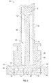
- FIG. 2 is a cross-sectional view of a chip collector body according to an embodiment of the invention.
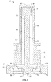
- FIG. 3 is a cross-sectional view of a chip collector body according to an embodiment of the invention.
- the magnetic chip collector 20 used to collect chips from a lubricant, such as in a gearbox or starter for example, is illustrated.
- the magnetic chip collector 20 includes a generally static housing 22 consisting of an elongate annular body 24 having a substantially hollow interior 26.
- the annular body includes an inlet 28 and an outlet 30 such that a lubricant may flow through a portion of the hollow interior 26.
- a chip collector body 40 is removably insertable into the hollow interior 26 of the annular body 30 to prevent drainage of the lubricant from within the housing 22.
- lubricant flows directly adjacent a portion, such as the second end 44 for example, of the chip collector body 40.
- the chip collector body 40 is provided in more detail in FIGS. 2 and 3 .
- the chip collector body 40 includes a base 46 positioned at a first end 42.
- the exterior 48 of the base 46 is generally contoured to block the hollow interior 26 of the housing 22, to prevent lubricant from leaking therefrom.
- An elongate member 50 extends from the base 46 to a second end 44 of the chip collector body 40.
- the base 46 and elongate member 50 are formed integrally from a ferrous material.
- the chip collector body 40 is formed with a hollow interior 52 extending from the first end 42 to adjacent the second end 44 such that the base 46 and elongate member 50 form a substantially hollow shell.
- the cross-section of the hollow interior 52 may be non-uniform over the length of the chip collector body 40.
- a first portion 54 of the hollow interior 52 adjacent the first end 42 of the chip collector body 40 has a width larger than a second portion 56 of the hollow interior 52 extending from the base 46 through the elongate member 50.
- a collector element 70 is also positioned within the hollow interior 52 and extends from the first end 42 to adjacent the second end 44 of the chip collector body 40.
- a magnetic element 76 such as a permanent magnet for example.
- a flange 78 Positioned near the second end 74 of the collector element 70 is a flange 78.
- the flange 78 is arranged within the hollow interior 52 adjacent both the first portion 54 and the second portion 56.
- the diameter of the flange 78 is larger than the diameter of the collector element 70 extending between the flange 78 and the magnetic element 76.
- a substantially flat disc 60 having a rigid surface, for example a washer.
- a retaining device 62 such as a retaining clip for example, is positioned within the hollow interior 52 directly adjacent a surface of the disc 60, and between the disc 60 and the first end 42. The edges of the retaining device 62 are arranged within an inlet 58 of the hollow interior 52 such that the retaining device 62 is prohibited from moving relative to the base 46.
- the diameter of the retaining device 62 is larger than the diameter of the disc 60.
- the retaining device 62 serves to keep the disc 60 within the chip collector body 40.
- the second end 74 of the collector element 70 protrudes through a central hole in both the disc 60 and the retaining device 62.
- the second end 74 of the collector element 70 includes a through bore 80 such that a ring or other device (not shown) for applying a force to the collector element 70 may be connected thereto.
- an axial biasing member 64 Positioned between the flange 78 of the collector element 70 and the disc 60 is an axial biasing member 64, such as a wave spring or coil spring for example.
- the collector element 70 is configured to move relative to the chip collector body 40 between a first position and a second position to selectively demagnetize the chip collector body 40.
- the collector element 70 When the collector element 70 is in the first position ( FIG. 2 ), the magnetic element 76 located at the first end 72 of the collector element 70 directly contacts the second end 44 of the chip collector body 40.
- an air gap 80 exists between the magnetic element 76 and the second end 44 of the chip collector body 40.
- Lubricant flows through the housing 22 ( FIG. 1 ) adjacent the second end 44 of the chip collector body 40 when the chip collector body 40 is installed within the hollow interior 26 of the housing 22.
- the collector element 70 When the collector element 70 is in the first position, the chip collector body 40 actively attracts magnetic particles in the lubricant to the second end 44 as a result of the magnetic force created at the second end 44 by contact with the magnetic element 76.
- an axial force is applied to the second end 74 of the collector element 70, such as through a ring or other device connected thereto.
- the flange 78 compresses the axial biasing member 64 against the rigid surface of the disc 60.
- the axial deformation of the biasing member 64 allows the collector element 70 to translate such that an air gap 82 is formed between the first end 72 of the collector element 70 and the second end 44 of the chip collector body 40.
- magnetic particles are no longer attracted to the second end 44 of the chip collector body 40 because the gap 82 prevents the magnetic force generated by the magnetic element 76 from transferring to the second end 44.
- the magnetic particles are easily removed from the second end 44, such as by wiping the body 40 with a cloth for example.
- the axial biasing member 64 will bias the collector element 70 back to the first position.
- the collector element 70 may be moved to selectively demagnetize the chip collector body 40, the ease of removing of magnetic particles from the second end 44 of the chip collector body 40 is significantly improved.
- the percentage of particles being removed from the chip collector body 40 will increase because the magnetic force from the magnetic element 76 will not act on the particles as they are removed. This in turn, will allow for a more accurate analysis of the wear occurring within the system.
Landscapes
- Sampling And Sample Adjustment (AREA)
- Lubrication Details And Ventilation Of Internal Combustion Engines (AREA)
- Coils Or Transformers For Communication (AREA)
- Fixed Capacitors And Capacitor Manufacturing Machines (AREA)
Abstract
Description
- Exemplary embodiments of this invention generally relate to magnetic chip collectors for collecting debris in a fluid and, more particularly, to a system and method for removing collected debris from a magnetic chip collector.
- Moving pieces in a machine, such as gears and bearings for example are subjected to wear phenomena. This wear can result in debris liberated from the moving pieces entering the lubrication system of the machine. Monitoring the level of debris in the lubricant circulation system can provide an indication of such abnormal component wear requiring maintenance action. In more detail, component wear in a propulsion system (i.e. wear associated with bearing, gears, shafts and the like) is typically evidenced by particulate metal that has been removed from the component through wear and deposited in a circulating lubricant, such as oil for example. Thus, by analyzing the type and amount of metal particles in a propulsion system's circulating lubricant, an operator can assess the relative health of the propulsion system components to facilitate maintenance decisions.
- A magnetic chip collector, which collects particles in the proximity of a magnetic collection element, may be used to detect wear debris in a lubricant system. Magnetic chip collectors require operators to periodically remove the collected chips to allow for physical inspection and determination of the type and amount of wear debris that has been collected. When operators attempt to remove the magnetic particles, such as by wiping the magnetic chip collector with a cloth, many of the particles remain attached to the magnetic chip collector as a result of the magnetic force. In addition, the magnetic force may act on some of the particles on the cloth, attracting them from the cloth back to the magnetic chip collector.
- According to one embodiment of the invention, a chip collector body is provided including a coupled base and elongate member. The base and elongate member have a substantially hollow interior extending from a first end to a second end, so as to form a shell. A collector element is positioned within the hollow interior. The collector element has a magnetic element positioned adjacent the second end and a flange positioned near the first end. The collector element is configured to move between a first position and a second position to selectively demagnetize the chip collector body. An axial biasing member is positioned between the flange of the collector element and a rigid surface. The axial biasing member is configured to bias the collector element into the first position.
- According to another embodiment of the invention, a method for removing magnetic particles from a chip collector body of a magnetic chip collector is provided including separating the chip collector body from a housing. The chip collector body is then demagnetized, and the magnetic particles are removed from a first end of the chip collector body.
- The subject matter, which is regarded as the invention, is particularly pointed out and distinctly claimed in the claims at the conclusion of the specification. The foregoing and other features, and advantages of the invention are apparent from the following detailed description taken in conjunction with the accompanying drawings in which:
-
FIG. 1 is a perspective view of an exemplary magnetic chip collector; -
FIG. 2 is a cross-sectional view of a chip collector body according to an embodiment of the invention; and -
FIG. 3 is a cross-sectional view of a chip collector body according to an embodiment of the invention. - The detailed description explains embodiments of the invention, together with advantages and features, by way of example with reference to the drawings.
- Referring to
FIG. 1 , amagnetic chip collector 20 used to collect chips from a lubricant, such as in a gearbox or starter for example, is illustrated. Themagnetic chip collector 20 includes a generallystatic housing 22 consisting of an elongateannular body 24 having a substantiallyhollow interior 26. In one embodiment, the annular body includes aninlet 28 and anoutlet 30 such that a lubricant may flow through a portion of thehollow interior 26. Achip collector body 40 is removably insertable into thehollow interior 26 of theannular body 30 to prevent drainage of the lubricant from within thehousing 22. When thechip collector body 40 is located within thehollow interior 26 of thehousing 22, lubricant flows directly adjacent a portion, such as thesecond end 44 for example, of thechip collector body 40. - The
chip collector body 40 is provided in more detail inFIGS. 2 and3 . Thechip collector body 40 includes abase 46 positioned at afirst end 42. As is known in the art, theexterior 48 of thebase 46 is generally contoured to block thehollow interior 26 of thehousing 22, to prevent lubricant from leaking therefrom. Anelongate member 50 extends from thebase 46 to asecond end 44 of thechip collector body 40. In one embodiment, thebase 46 andelongate member 50 are formed integrally from a ferrous material. Similar to thehousing 22, thechip collector body 40 is formed with ahollow interior 52 extending from thefirst end 42 to adjacent thesecond end 44 such that thebase 46 andelongate member 50 form a substantially hollow shell. The cross-section of thehollow interior 52 may be non-uniform over the length of thechip collector body 40. In one embodiment, afirst portion 54 of thehollow interior 52 adjacent thefirst end 42 of thechip collector body 40 has a width larger than asecond portion 56 of thehollow interior 52 extending from thebase 46 through theelongate member 50. - A
collector element 70 is also positioned within thehollow interior 52 and extends from thefirst end 42 to adjacent thesecond end 44 of thechip collector body 40. Arranged at afirst end 72 of thecollector element 70 is amagnetic element 76, such as a permanent magnet for example. Positioned near thesecond end 74 of thecollector element 70 is aflange 78. In one embodiment, theflange 78 is arranged within thehollow interior 52 adjacent both thefirst portion 54 and thesecond portion 56. In one embodiment, the diameter of theflange 78 is larger than the diameter of thecollector element 70 extending between theflange 78 and themagnetic element 76. - Mounted near the
first end 42 of thechip collector body 40, within thefirst portion 54 of thehollow interior 52, is a substantiallyflat disc 60 having a rigid surface, for example a washer. Aretaining device 62, such as a retaining clip for example, is positioned within thehollow interior 52 directly adjacent a surface of thedisc 60, and between thedisc 60 and thefirst end 42. The edges of theretaining device 62 are arranged within aninlet 58 of thehollow interior 52 such that theretaining device 62 is prohibited from moving relative to thebase 46. In one embodiment, the diameter of theretaining device 62 is larger than the diameter of thedisc 60. Thus, theretaining device 62 serves to keep thedisc 60 within thechip collector body 40. - The
second end 74 of thecollector element 70 protrudes through a central hole in both thedisc 60 and theretaining device 62. In one non-limiting embodiment, thesecond end 74 of thecollector element 70 includes a throughbore 80 such that a ring or other device (not shown) for applying a force to thecollector element 70 may be connected thereto. Positioned between theflange 78 of thecollector element 70 and thedisc 60 is anaxial biasing member 64, such as a wave spring or coil spring for example. - The
collector element 70 is configured to move relative to thechip collector body 40 between a first position and a second position to selectively demagnetize thechip collector body 40. When thecollector element 70 is in the first position (FIG. 2 ), themagnetic element 76 located at thefirst end 72 of thecollector element 70 directly contacts thesecond end 44 of thechip collector body 40. As illustrated inFIG. 3 , when thecollector element 70 is in the second position, anair gap 80 exists between themagnetic element 76 and thesecond end 44 of thechip collector body 40. Lubricant flows through the housing 22 (FIG. 1 ) adjacent thesecond end 44 of thechip collector body 40 when thechip collector body 40 is installed within thehollow interior 26 of thehousing 22. When thecollector element 70 is in the first position, thechip collector body 40 actively attracts magnetic particles in the lubricant to thesecond end 44 as a result of the magnetic force created at thesecond end 44 by contact with themagnetic element 76. - To move the
collector element 70 to the second position, an axial force is applied to thesecond end 74 of thecollector element 70, such as through a ring or other device connected thereto. As a result, theflange 78 compresses theaxial biasing member 64 against the rigid surface of thedisc 60. The axial deformation of thebiasing member 64 allows thecollector element 70 to translate such that anair gap 82 is formed between thefirst end 72 of thecollector element 70 and thesecond end 44 of thechip collector body 40. In this second position, magnetic particles are no longer attracted to thesecond end 44 of thechip collector body 40 because thegap 82 prevents the magnetic force generated by themagnetic element 76 from transferring to thesecond end 44. When thechip collector body 40 is demagnetized, the magnetic particles are easily removed from thesecond end 44, such as by wiping thebody 40 with a cloth for example. Once the force is removed from thesecond end 74 of thecollector element 70, theaxial biasing member 64 will bias thecollector element 70 back to the first position. - Because the
collector element 70 may be moved to selectively demagnetize thechip collector body 40, the ease of removing of magnetic particles from thesecond end 44 of thechip collector body 40 is significantly improved. In addition, the percentage of particles being removed from thechip collector body 40 will increase because the magnetic force from themagnetic element 76 will not act on the particles as they are removed. This in turn, will allow for a more accurate analysis of the wear occurring within the system. - While the invention has been described in detail in connection with only a limited number of embodiments, it should be readily understood that the invention is not limited to such disclosed embodiments. Rather, the invention can be modified to incorporate any number of variations, alterations, substitutions or equivalent arrangements not heretofore described, but which are commensurate with the spirit and scope of the invention. Additionally, while various embodiments of the invention have been described, it is to be understood that aspects of the invention may include only some of the described embodiments. Accordingly, the invention is not to be seen as limited by the foregoing description, but is only limited by the scope of the appended claims.
Claims (12)
- A chip collector body (40) comprising:a coupled base (46) and elongate member (50) having a substantially hollow interior (52) extending from a first end to a second end so as to form a shell;a collector element (70) positioned within the hollow interior (52) having a magnetic element (76) positioned adjacent the second end and a flange (78) near the first end, the collector element (70) is configured to move between a first position and a second position to selectively demagnetize the chip collector body; andan axial biasing member (64) positioned between the flange (78) of the collector element (70) and a rigid surface, wherein the axial biasing member is configured to bias the collector element into the first position.
- The chip collector body (40) according to claim 1, wherein when in the first position, the magnetic element (76) is adjacent the second end and when in the second position an air gap (82) exists between the magnetic element (76) and the second end.
- The chip collector body according to any preceding claim, wherein the axial biasing member (64) is a wave spring.
- The chip collector body (40) according to any preceding claim,
wherein the base (46) and elongate member (50) are integrally formed from a ferrous material. - The chip collector body according to any preceding claim, further comprising a retainer device (62) positioned adjacent the rigid surface, wherein the retainer device is configured to prevent movement of the rigid surface within the hollow interior (52).
- The chip collector body according to claim 5, wherein the rigid surface is a washer.
- The chip collector body according to any preceding claim, wherein an exterior of the base (46) is contoured to block a fluid flow from exiting a housing of a magnetic chip detector when connected to the housing.
- A method for removing magnetic particles from a chip collector body (40) of a magnetic chip collector (20) comprising:separating the chip collector body (40) from a housing (22);demagnetizing the chip collector body (40); andremoving the magnetic particles from a first end of the chip collector body (40).
- The method according to claim 8, wherein the chip collector body (40) is demagnetized by applying a force to a portion of a collector element (70) housed within a hollow interior (52) of the chip collector body (40).
- The method according to claim 9, wherein application of a force causes a magnetic element (76) mounted at a second end of the collector element (70) to move from a first position to a second position.
- The method according to claim 10, wherein in the first position the magnetic portion is in contact with the first end of the chip collector body (40) and in the second position, an air gap (82) exists between the magnetic portion and the first end of the chip collector body (40).
- The method according to claim 8, wherein the magnetic particles are removed by wiping the first end of the chip collector body (40) with a cloth.
Applications Claiming Priority (1)
| Application Number | Priority Date | Filing Date | Title |
|---|---|---|---|
| US13/668,983 US20140124449A1 (en) | 2012-11-05 | 2012-11-05 | System and method for clearing chips from a magnetic chip collector |
Publications (3)
| Publication Number | Publication Date |
|---|---|
| EP2727651A2 true EP2727651A2 (en) | 2014-05-07 |
| EP2727651A3 EP2727651A3 (en) | 2017-04-26 |
| EP2727651B1 EP2727651B1 (en) | 2018-09-05 |
Family
ID=49552178
Family Applications (1)
| Application Number | Title | Priority Date | Filing Date |
|---|---|---|---|
| EP13190877.4A Active EP2727651B1 (en) | 2012-11-05 | 2013-10-30 | System for clearing chips from a magnetic chip collector |
Country Status (2)
| Country | Link |
|---|---|
| US (1) | US20140124449A1 (en) |
| EP (1) | EP2727651B1 (en) |
Family Cites Families (8)
| Publication number | Priority date | Publication date | Assignee | Title |
|---|---|---|---|---|
| US2693979A (en) * | 1950-08-03 | 1954-11-09 | George L Russell | Magnetic device |
| US2970002A (en) * | 1959-01-20 | 1961-01-31 | Laviano Samuel | Magnetic pickup |
| US3771084A (en) * | 1972-08-25 | 1973-11-06 | Xerox Corp | Magnetic retrieval device |
| US4446019A (en) * | 1982-09-16 | 1984-05-01 | Donaldson Company, Inc. | Magnetic filtration in a spin-on fluid filter |
| SE8601143L (en) * | 1986-03-12 | 1987-09-13 | Carbematrix Ab | SET AND DEVICE FOR COLLECTION AND DISTRIBUTION OF FERROMAGNETIC PARTICLES IN A FLUID MEDIUM |
| US5433492A (en) * | 1994-03-01 | 1995-07-18 | Tdw Delaware, Inc. | Ferrous chip removal tool |
| US5639074A (en) * | 1996-03-05 | 1997-06-17 | Smalley Steel Ring Co. | Interlaced wave spring |
| US6445177B1 (en) * | 1999-11-17 | 2002-09-03 | Vibro-Meter S.A. | Chip-detector assembly having improved probe-retention features |
-
2012
- 2012-11-05 US US13/668,983 patent/US20140124449A1/en not_active Abandoned
-
2013
- 2013-10-30 EP EP13190877.4A patent/EP2727651B1/en active Active
Non-Patent Citations (1)
| Title |
|---|
| None |
Also Published As
| Publication number | Publication date |
|---|---|
| EP2727651A3 (en) | 2017-04-26 |
| EP2727651B1 (en) | 2018-09-05 |
| US20140124449A1 (en) | 2014-05-08 |
Similar Documents
| Publication | Publication Date | Title |
|---|---|---|
| JP7257970B2 (en) | Bearing monitoring/analysis system | |
| JPH06323335A (en) | Roller bearing device | |
| EP2151596B1 (en) | Device for capturing and/or retaining brake dust of a braking unit and corresponding brake unit | |
| KR102371348B1 (en) | A method and a system for monitoring a lubricated mechanical system | |
| CN103477102A (en) | Roller bearing, and travel device provided with roller bearing | |
| EP0126554B1 (en) | Recirculating lubricating system | |
| JP2008530462A (en) | Conical roller bearing with filter cage | |
| Tandon et al. | Condition monitoring of electric motor ball bearings for the detection of grease contaminants | |
| DE112017006272T5 (en) | Rolling bearing with rotation sensor | |
| CN108884875B (en) | Rolling bearing unit | |
| JP2002536604A (en) | Bearing isolator | |
| US10094424B2 (en) | Rolling bearing | |
| US20140124449A1 (en) | System and method for clearing chips from a magnetic chip collector | |
| CN102418783A (en) | Device for filtering lubricant in a transmission | |
| JP2016166625A (en) | Rolling bearing with filter | |
| US20260002585A1 (en) | System and method for detecting the presence of as well as for analyzing particles in a flow of lubricant | |
| CN220399330U (en) | Main shaft bearing internal damage detecting system based on magnetic field induction | |
| CN106907462A (en) | Chip captures magnet structure | |
| JP3707499B1 (en) | Method for removing dust from equipment having sliding parts | |
| JP6824453B1 (en) | Transmission mechanism with monitoring function | |
| Showalter et al. | Oil debris monitoring in aerospace engines and helicopter transmissions | |
| JP2012202444A (en) | Rolling bearing with filter | |
| Haran et al. | ANALYSIS OF BEARING FAILURE DUE TO COOLANT OIL CONTAMINATION USING DIAGNOSTIC TECHNIQUES IN GRINDING | |
| CN109563883A (en) | Piecing devices for articulated shaft | |
| EP2886318A1 (en) | Self lubricating robust centralizer bearing design and method of use |
Legal Events
| Date | Code | Title | Description |
|---|---|---|---|
| PUAI | Public reference made under article 153(3) epc to a published international application that has entered the european phase |
Free format text: ORIGINAL CODE: 0009012 |
|
| 17P | Request for examination filed |
Effective date: 20131030 |
|
| AK | Designated contracting states |
Kind code of ref document: A2 Designated state(s): AL AT BE BG CH CY CZ DE DK EE ES FI FR GB GR HR HU IE IS IT LI LT LU LV MC MK MT NL NO PL PT RO RS SE SI SK SM TR |
|
| AX | Request for extension of the european patent |
Extension state: BA ME |
|
| PUAL | Search report despatched |
Free format text: ORIGINAL CODE: 0009013 |
|
| AK | Designated contracting states |
Kind code of ref document: A3 Designated state(s): AL AT BE BG CH CY CZ DE DK EE ES FI FR GB GR HR HU IE IS IT LI LT LU LV MC MK MT NL NO PL PT RO RS SE SI SK SM TR |
|
| AX | Request for extension of the european patent |
Extension state: BA ME |
|
| RIC1 | Information provided on ipc code assigned before grant |
Ipc: B03C 1/28 20060101AFI20170323BHEP Ipc: B03C 1/033 20060101ALI20170323BHEP |
|
| STAA | Information on the status of an ep patent application or granted ep patent |
Free format text: STATUS: REQUEST FOR EXAMINATION WAS MADE |
|
| 17P | Request for examination filed |
Effective date: 20171026 |
|
| RBV | Designated contracting states (corrected) |
Designated state(s): AL AT BE BG CH CY CZ DE DK EE ES FI FR GB GR HR HU IE IS IT LI LT LU LV MC MK MT NL NO PL PT RO RS SE SI SK SM TR |
|
| GRAP | Despatch of communication of intention to grant a patent |
Free format text: ORIGINAL CODE: EPIDOSNIGR1 |
|
| STAA | Information on the status of an ep patent application or granted ep patent |
Free format text: STATUS: GRANT OF PATENT IS INTENDED |
|
| INTG | Intention to grant announced |
Effective date: 20180313 |
|
| GRAS | Grant fee paid |
Free format text: ORIGINAL CODE: EPIDOSNIGR3 |
|
| GRAA | (expected) grant |
Free format text: ORIGINAL CODE: 0009210 |
|
| STAA | Information on the status of an ep patent application or granted ep patent |
Free format text: STATUS: THE PATENT HAS BEEN GRANTED |
|
| AK | Designated contracting states |
Kind code of ref document: B1 Designated state(s): AL AT BE BG CH CY CZ DE DK EE ES FI FR GB GR HR HU IE IS IT LI LT LU LV MC MK MT NL NO PL PT RO RS SE SI SK SM TR |
|
| REG | Reference to a national code |
Ref country code: GB Ref legal event code: FG4D |
|
| REG | Reference to a national code |
Ref country code: CH Ref legal event code: EP |
|
| REG | Reference to a national code |
Ref country code: AT Ref legal event code: REF Ref document number: 1037215 Country of ref document: AT Kind code of ref document: T Effective date: 20180915 |
|
| REG | Reference to a national code |
Ref country code: IE Ref legal event code: FG4D |
|
| REG | Reference to a national code |
Ref country code: DE Ref legal event code: R096 Ref document number: 602013043045 Country of ref document: DE |
|
| REG | Reference to a national code |
Ref country code: FR Ref legal event code: PLFP Year of fee payment: 6 |
|
| REG | Reference to a national code |
Ref country code: NL Ref legal event code: MP Effective date: 20180905 |
|
| REG | Reference to a national code |
Ref country code: LT Ref legal event code: MG4D |
|
| PG25 | Lapsed in a contracting state [announced via postgrant information from national office to epo] |
Ref country code: GR Free format text: LAPSE BECAUSE OF FAILURE TO SUBMIT A TRANSLATION OF THE DESCRIPTION OR TO PAY THE FEE WITHIN THE PRESCRIBED TIME-LIMIT Effective date: 20181206 Ref country code: NO Free format text: LAPSE BECAUSE OF FAILURE TO SUBMIT A TRANSLATION OF THE DESCRIPTION OR TO PAY THE FEE WITHIN THE PRESCRIBED TIME-LIMIT Effective date: 20181205 Ref country code: FI Free format text: LAPSE BECAUSE OF FAILURE TO SUBMIT A TRANSLATION OF THE DESCRIPTION OR TO PAY THE FEE WITHIN THE PRESCRIBED TIME-LIMIT Effective date: 20180905 Ref country code: RS Free format text: LAPSE BECAUSE OF FAILURE TO SUBMIT A TRANSLATION OF THE DESCRIPTION OR TO PAY THE FEE WITHIN THE PRESCRIBED TIME-LIMIT Effective date: 20180905 Ref country code: SE Free format text: LAPSE BECAUSE OF FAILURE TO SUBMIT A TRANSLATION OF THE DESCRIPTION OR TO PAY THE FEE WITHIN THE PRESCRIBED TIME-LIMIT Effective date: 20180905 Ref country code: BG Free format text: LAPSE BECAUSE OF FAILURE TO SUBMIT A TRANSLATION OF THE DESCRIPTION OR TO PAY THE FEE WITHIN THE PRESCRIBED TIME-LIMIT Effective date: 20181205 Ref country code: LT Free format text: LAPSE BECAUSE OF FAILURE TO SUBMIT A TRANSLATION OF THE DESCRIPTION OR TO PAY THE FEE WITHIN THE PRESCRIBED TIME-LIMIT Effective date: 20180905 |
|
| REG | Reference to a national code |
Ref country code: AT Ref legal event code: MK05 Ref document number: 1037215 Country of ref document: AT Kind code of ref document: T Effective date: 20180905 |
|
| PG25 | Lapsed in a contracting state [announced via postgrant information from national office to epo] |
Ref country code: AL Free format text: LAPSE BECAUSE OF FAILURE TO SUBMIT A TRANSLATION OF THE DESCRIPTION OR TO PAY THE FEE WITHIN THE PRESCRIBED TIME-LIMIT Effective date: 20180905 Ref country code: LV Free format text: LAPSE BECAUSE OF FAILURE TO SUBMIT A TRANSLATION OF THE DESCRIPTION OR TO PAY THE FEE WITHIN THE PRESCRIBED TIME-LIMIT Effective date: 20180905 Ref country code: HR Free format text: LAPSE BECAUSE OF FAILURE TO SUBMIT A TRANSLATION OF THE DESCRIPTION OR TO PAY THE FEE WITHIN THE PRESCRIBED TIME-LIMIT Effective date: 20180905 |
|
| PG25 | Lapsed in a contracting state [announced via postgrant information from national office to epo] |
Ref country code: ES Free format text: LAPSE BECAUSE OF FAILURE TO SUBMIT A TRANSLATION OF THE DESCRIPTION OR TO PAY THE FEE WITHIN THE PRESCRIBED TIME-LIMIT Effective date: 20180905 Ref country code: IS Free format text: LAPSE BECAUSE OF FAILURE TO SUBMIT A TRANSLATION OF THE DESCRIPTION OR TO PAY THE FEE WITHIN THE PRESCRIBED TIME-LIMIT Effective date: 20190105 Ref country code: NL Free format text: LAPSE BECAUSE OF FAILURE TO SUBMIT A TRANSLATION OF THE DESCRIPTION OR TO PAY THE FEE WITHIN THE PRESCRIBED TIME-LIMIT Effective date: 20180905 Ref country code: PL Free format text: LAPSE BECAUSE OF FAILURE TO SUBMIT A TRANSLATION OF THE DESCRIPTION OR TO PAY THE FEE WITHIN THE PRESCRIBED TIME-LIMIT Effective date: 20180905 Ref country code: CZ Free format text: LAPSE BECAUSE OF FAILURE TO SUBMIT A TRANSLATION OF THE DESCRIPTION OR TO PAY THE FEE WITHIN THE PRESCRIBED TIME-LIMIT Effective date: 20180905 Ref country code: RO Free format text: LAPSE BECAUSE OF FAILURE TO SUBMIT A TRANSLATION OF THE DESCRIPTION OR TO PAY THE FEE WITHIN THE PRESCRIBED TIME-LIMIT Effective date: 20180905 Ref country code: EE Free format text: LAPSE BECAUSE OF FAILURE TO SUBMIT A TRANSLATION OF THE DESCRIPTION OR TO PAY THE FEE WITHIN THE PRESCRIBED TIME-LIMIT Effective date: 20180905 Ref country code: AT Free format text: LAPSE BECAUSE OF FAILURE TO SUBMIT A TRANSLATION OF THE DESCRIPTION OR TO PAY THE FEE WITHIN THE PRESCRIBED TIME-LIMIT Effective date: 20180905 Ref country code: IT Free format text: LAPSE BECAUSE OF FAILURE TO SUBMIT A TRANSLATION OF THE DESCRIPTION OR TO PAY THE FEE WITHIN THE PRESCRIBED TIME-LIMIT Effective date: 20180905 |
|
| PG25 | Lapsed in a contracting state [announced via postgrant information from national office to epo] |
Ref country code: SM Free format text: LAPSE BECAUSE OF FAILURE TO SUBMIT A TRANSLATION OF THE DESCRIPTION OR TO PAY THE FEE WITHIN THE PRESCRIBED TIME-LIMIT Effective date: 20180905 Ref country code: SK Free format text: LAPSE BECAUSE OF FAILURE TO SUBMIT A TRANSLATION OF THE DESCRIPTION OR TO PAY THE FEE WITHIN THE PRESCRIBED TIME-LIMIT Effective date: 20180905 Ref country code: PT Free format text: LAPSE BECAUSE OF FAILURE TO SUBMIT A TRANSLATION OF THE DESCRIPTION OR TO PAY THE FEE WITHIN THE PRESCRIBED TIME-LIMIT Effective date: 20190105 |
|
| REG | Reference to a national code |
Ref country code: CH Ref legal event code: PL |
|
| REG | Reference to a national code |
Ref country code: DE Ref legal event code: R097 Ref document number: 602013043045 Country of ref document: DE |
|
| REG | Reference to a national code |
Ref country code: BE Ref legal event code: MM Effective date: 20181031 |
|
| PG25 | Lapsed in a contracting state [announced via postgrant information from national office to epo] |
Ref country code: LU Free format text: LAPSE BECAUSE OF NON-PAYMENT OF DUE FEES Effective date: 20181030 |
|
| PLBE | No opposition filed within time limit |
Free format text: ORIGINAL CODE: 0009261 |
|
| STAA | Information on the status of an ep patent application or granted ep patent |
Free format text: STATUS: NO OPPOSITION FILED WITHIN TIME LIMIT |
|
| REG | Reference to a national code |
Ref country code: IE Ref legal event code: MM4A |
|
| PG25 | Lapsed in a contracting state [announced via postgrant information from national office to epo] |
Ref country code: MC Free format text: LAPSE BECAUSE OF FAILURE TO SUBMIT A TRANSLATION OF THE DESCRIPTION OR TO PAY THE FEE WITHIN THE PRESCRIBED TIME-LIMIT Effective date: 20180905 Ref country code: DK Free format text: LAPSE BECAUSE OF FAILURE TO SUBMIT A TRANSLATION OF THE DESCRIPTION OR TO PAY THE FEE WITHIN THE PRESCRIBED TIME-LIMIT Effective date: 20180905 |
|
| 26N | No opposition filed |
Effective date: 20190606 |
|
| PG25 | Lapsed in a contracting state [announced via postgrant information from national office to epo] |
Ref country code: SI Free format text: LAPSE BECAUSE OF FAILURE TO SUBMIT A TRANSLATION OF THE DESCRIPTION OR TO PAY THE FEE WITHIN THE PRESCRIBED TIME-LIMIT Effective date: 20180905 Ref country code: BE Free format text: LAPSE BECAUSE OF NON-PAYMENT OF DUE FEES Effective date: 20181031 Ref country code: CH Free format text: LAPSE BECAUSE OF NON-PAYMENT OF DUE FEES Effective date: 20181031 Ref country code: LI Free format text: LAPSE BECAUSE OF NON-PAYMENT OF DUE FEES Effective date: 20181031 |
|
| PG25 | Lapsed in a contracting state [announced via postgrant information from national office to epo] |
Ref country code: IE Free format text: LAPSE BECAUSE OF NON-PAYMENT OF DUE FEES Effective date: 20181030 |
|
| PG25 | Lapsed in a contracting state [announced via postgrant information from national office to epo] |
Ref country code: MT Free format text: LAPSE BECAUSE OF NON-PAYMENT OF DUE FEES Effective date: 20181030 |
|
| PG25 | Lapsed in a contracting state [announced via postgrant information from national office to epo] |
Ref country code: TR Free format text: LAPSE BECAUSE OF FAILURE TO SUBMIT A TRANSLATION OF THE DESCRIPTION OR TO PAY THE FEE WITHIN THE PRESCRIBED TIME-LIMIT Effective date: 20180905 |
|
| PG25 | Lapsed in a contracting state [announced via postgrant information from national office to epo] |
Ref country code: HU Free format text: LAPSE BECAUSE OF FAILURE TO SUBMIT A TRANSLATION OF THE DESCRIPTION OR TO PAY THE FEE WITHIN THE PRESCRIBED TIME-LIMIT; INVALID AB INITIO Effective date: 20131030 Ref country code: CY Free format text: LAPSE BECAUSE OF FAILURE TO SUBMIT A TRANSLATION OF THE DESCRIPTION OR TO PAY THE FEE WITHIN THE PRESCRIBED TIME-LIMIT Effective date: 20180905 Ref country code: MK Free format text: LAPSE BECAUSE OF NON-PAYMENT OF DUE FEES Effective date: 20180905 |
|
| P01 | Opt-out of the competence of the unified patent court (upc) registered |
Effective date: 20230522 |
|
| PGFP | Annual fee paid to national office [announced via postgrant information from national office to epo] |
Ref country code: GB Payment date: 20250923 Year of fee payment: 13 |
|
| PGFP | Annual fee paid to national office [announced via postgrant information from national office to epo] |
Ref country code: FR Payment date: 20250924 Year of fee payment: 13 |
|
| PGFP | Annual fee paid to national office [announced via postgrant information from national office to epo] |
Ref country code: DE Payment date: 20250923 Year of fee payment: 13 |