EP2725615A1 - Semiconductor device comprising a diode and method for producing such a device - Google Patents
Semiconductor device comprising a diode and method for producing such a device Download PDFInfo
- Publication number
- EP2725615A1 EP2725615A1 EP12190455.1A EP12190455A EP2725615A1 EP 2725615 A1 EP2725615 A1 EP 2725615A1 EP 12190455 A EP12190455 A EP 12190455A EP 2725615 A1 EP2725615 A1 EP 2725615A1
- Authority
- EP
- European Patent Office
- Prior art keywords
- active area
- area
- doping
- upper portion
- active
- Prior art date
- Legal status (The legal status is an assumption and is not a legal conclusion. Google has not performed a legal analysis and makes no representation as to the accuracy of the status listed.)
- Granted
Links
Images

Classifications
-
- H—ELECTRICITY
- H10—SEMICONDUCTOR DEVICES; ELECTRIC SOLID-STATE DEVICES NOT OTHERWISE PROVIDED FOR
- H10W—GENERIC PACKAGES, INTERCONNECTIONS, CONNECTORS OR OTHER CONSTRUCTIONAL DETAILS OF DEVICES COVERED BY CLASS H10
- H10W42/00—Arrangements for protection of devices
- H10W42/60—Arrangements for protection of devices protecting against electrostatic charges or discharges, e.g. Faraday shields
-
- H—ELECTRICITY
- H10—SEMICONDUCTOR DEVICES; ELECTRIC SOLID-STATE DEVICES NOT OTHERWISE PROVIDED FOR
- H10D—INORGANIC ELECTRIC SEMICONDUCTOR DEVICES
- H10D10/00—Bipolar junction transistors [BJT]
- H10D10/01—Manufacture or treatment
-
- H—ELECTRICITY
- H10—SEMICONDUCTOR DEVICES; ELECTRIC SOLID-STATE DEVICES NOT OTHERWISE PROVIDED FOR
- H10D—INORGANIC ELECTRIC SEMICONDUCTOR DEVICES
- H10D62/00—Semiconductor bodies, or regions thereof, of devices having potential barriers
- H10D62/10—Shapes, relative sizes or dispositions of the regions of the semiconductor bodies; Shapes of the semiconductor bodies
- H10D62/124—Shapes, relative sizes or dispositions of the regions of semiconductor bodies or of junctions between the regions
- H10D62/125—Shapes of junctions between the regions
-
- H—ELECTRICITY
- H10—SEMICONDUCTOR DEVICES; ELECTRIC SOLID-STATE DEVICES NOT OTHERWISE PROVIDED FOR
- H10D—INORGANIC ELECTRIC SEMICONDUCTOR DEVICES
- H10D62/00—Semiconductor bodies, or regions thereof, of devices having potential barriers
- H10D62/60—Impurity distributions or concentrations
-
- H—ELECTRICITY
- H10—SEMICONDUCTOR DEVICES; ELECTRIC SOLID-STATE DEVICES NOT OTHERWISE PROVIDED FOR
- H10D—INORGANIC ELECTRIC SEMICONDUCTOR DEVICES
- H10D8/00—Diodes
- H10D8/01—Manufacture or treatment
-
- H—ELECTRICITY
- H10—SEMICONDUCTOR DEVICES; ELECTRIC SOLID-STATE DEVICES NOT OTHERWISE PROVIDED FOR
- H10D—INORGANIC ELECTRIC SEMICONDUCTOR DEVICES
- H10D8/00—Diodes
- H10D8/01—Manufacture or treatment
- H10D8/021—Manufacture or treatment of breakdown diodes
-
- H—ELECTRICITY
- H10—SEMICONDUCTOR DEVICES; ELECTRIC SOLID-STATE DEVICES NOT OTHERWISE PROVIDED FOR
- H10D—INORGANIC ELECTRIC SEMICONDUCTOR DEVICES
- H10D8/00—Diodes
- H10D8/01—Manufacture or treatment
- H10D8/021—Manufacture or treatment of breakdown diodes
- H10D8/022—Manufacture or treatment of breakdown diodes of Zener diodes
-
- H—ELECTRICITY
- H10—SEMICONDUCTOR DEVICES; ELECTRIC SOLID-STATE DEVICES NOT OTHERWISE PROVIDED FOR
- H10D—INORGANIC ELECTRIC SEMICONDUCTOR DEVICES
- H10D8/00—Diodes
- H10D8/20—Breakdown diodes, e.g. avalanche diodes
- H10D8/25—Zener diodes
-
- H—ELECTRICITY
- H10—SEMICONDUCTOR DEVICES; ELECTRIC SOLID-STATE DEVICES NOT OTHERWISE PROVIDED FOR
- H10D—INORGANIC ELECTRIC SEMICONDUCTOR DEVICES
- H10D84/00—Integrated devices formed in or on semiconductor substrates that comprise only semiconducting layers, e.g. on Si wafers or on GaAs-on-Si wafers
- H10D84/101—Integrated devices comprising main components and built-in components, e.g. IGBT having built-in freewheel diode
- H10D84/121—BJTs having built-in components
-
- H—ELECTRICITY
- H10—SEMICONDUCTOR DEVICES; ELECTRIC SOLID-STATE DEVICES NOT OTHERWISE PROVIDED FOR
- H10D—INORGANIC ELECTRIC SEMICONDUCTOR DEVICES
- H10D89/00—Aspects of integrated devices not covered by groups H10D84/00 - H10D88/00
- H10D89/60—Integrated devices comprising arrangements for electrical or thermal protection, e.g. protection circuits against electrostatic discharge [ESD]
- H10D89/601—Integrated devices comprising arrangements for electrical or thermal protection, e.g. protection circuits against electrostatic discharge [ESD] for devices having insulated gate electrodes, e.g. for IGFETs or IGBTs
- H10D89/611—Integrated devices comprising arrangements for electrical or thermal protection, e.g. protection circuits against electrostatic discharge [ESD] for devices having insulated gate electrodes, e.g. for IGFETs or IGBTs using diodes as protective elements
-
- H—ELECTRICITY
- H10—SEMICONDUCTOR DEVICES; ELECTRIC SOLID-STATE DEVICES NOT OTHERWISE PROVIDED FOR
- H10D—INORGANIC ELECTRIC SEMICONDUCTOR DEVICES
- H10D10/00—Bipolar junction transistors [BJT]
- H10D10/60—Lateral BJTs
-
- H—ELECTRICITY
- H10—SEMICONDUCTOR DEVICES; ELECTRIC SOLID-STATE DEVICES NOT OTHERWISE PROVIDED FOR
- H10D—INORGANIC ELECTRIC SEMICONDUCTOR DEVICES
- H10D62/00—Semiconductor bodies, or regions thereof, of devices having potential barriers
- H10D62/10—Shapes, relative sizes or dispositions of the regions of the semiconductor bodies; Shapes of the semiconductor bodies
- H10D62/113—Isolations within a component, i.e. internal isolations
- H10D62/115—Dielectric isolations, e.g. air gaps
Definitions
- the present invention is related to methods for producing a semiconductor device including a diode formed by a junction of differently doped areas in the substrate.
- the primary application is for the production of Integrated Circuit packages comprising IC's mounted on an interposer chip, provided with Electrostatic Discharge (ESD) protection on the interposer.
- ESD Electrostatic Discharge
- ESD protection devices are major examples of semiconductor devices comprising a diode junction.
- an optimization is needed in terms of the process technology itself, such as the number of process steps and the number of lithography masks applied in the process, in order to further obtain a cost reduction in the production of such devices, for example on an interposer chip,.
- the method and device of the invention provide a way of optimizing the production of a diode structure in a semiconductor device, such as an ESD protection device, making it more cost-effective to produce such devices in general and particularly on an interposer chip.
- the present invention is related to a semiconductor device comprising a diode junction between two semiconductor regions of different doping types, in particular between an upper portion of an active area and the remainder of said area, said active area being defined in a substrate surface between two field dielectric regions.
- the upper portion is a portion of the active area that is lower in width than the active area itself.
- the device of the invention is an ESD protection device comprising such a diode.
- the active area is provided with a doping profile, exhibiting a maximum value at the surface of said active area, and changing to a minimum value at a higher depth, said depth preferably being higher than half the depth of the upper portion.
- the diode does not require an ESD implant for lowering the holding voltage.
- the invention is in particular related to a device and method as disclosed in the appended claims.
- the invention is firstly related to a semiconductor device comprising a bulk substrate area lying underneath a plurality of field dielectric regions with active area's in between adjacent field dielectric regions, wherein one of said active areas and at least the part of the bulk substrate area underneath said active area is formed of material of a first doping type except for at least one upper portion of said active area that is located between the active area's surface and the depth of said upper portion, said upper portion being formed of material of the doping type opposite to the first doping type, wherein at least in a part of said active area, the width of said upper portion is smaller than the width of the active area, the device comprising a diode in said active area of the device, the diode being formed by at least part of the junction between said upper portion of the active area and the remainder of the active area, the upper portion being connected to a first terminal, the remainder of the active area being connected to a second terminal, and wherein a doping profile of
- said second terminal is connected to the surface of said remainder of the active area.
- said active area is a first active area, and said second terminal is connected to the surface of a second active area (26) of the same doping as said first active area (23).
- said profile is such that the doping level again changes to a second maximum value, at a higher depth than said minimum, said second maximum preferably being reached at a depth lying within said bulk substrate area.
- the device of the invention may be an ESD protection device comprising said diode and a bipolar transistor, arranged to conduct current from an ESD terminal to ground after the diode has gone into breakdown mode, the emitter and collector of said transistor being respectively formed by two areas of the same doping type as said upper portion of the (first) active area, said two areas that form the emitter and collector being formed respectively in two further active areas.
- said device is located on an interposer substrate on which one or more integrated circuit chips are mounted, said ESD protection device being configured to protect an electrical connection of an IC from electrostatic discharge.
- Said semiconductor may be silicon, said upper portion being n-doped and the remainder of said (first) active area being p-doped.
- said depth at which the minimum doping level is reached is higher than half the depth of said upper portion.
- the invention is also related to a method for producing a semiconductor device comprising a diode, comprising the steps of :
- said second terminal is connected to the surface of said remainder of the active area.
- said active area is a first active area, and said second terminal is connected to the surface of a second active area of the same doping as said first active area.
- said profile is such that the doping level again changes to a second maximum value, at a higher depth than said minimum, said second maximum preferably being reached at a depth lying within said bulk substrate area.
- said device may be an ESD protection device comprising a diode and a bipolar transistor, the emitter and collector being respectively formed in two further active areas, wherein in said deposition step, ions of said opposite type are deposited in said further active areas to form said emitter and collector.
- the step of producing connections from active areas to said terminals comprises a pre-metal dielectric deposition and patterning step to form contact holes, a contact formation step by filling said holes with a contact metal, and a silicidation step for forming silicide areas between the active areas and the contact metal, wherein said silicidation step is performed after the PMD patterning step and before the contact formation step.
- said depth at which the minimum doping level is reached is higher than half the depth of said upper portion.
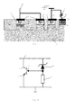
- Figure 1 illustrates a prior art ESD protection device structure.
- Figure 2 illustrates the electrical equivalent circuit of the device of figure 1 .
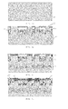
- Figures 3a to 3f illustrates the steps of the method according to a preferred embodiment of the invention.
- Figure 4 shows an example of a p-doping profile implanted in the method step illustrated by figure 3c .
- Figure 5 illustrates the shape of the diode's p-n junction in a device produced according to the invention.
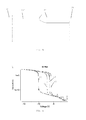
- Figure 6 illustrates the influence of the p-dopant level in the area adjacent to the n-doped area, on the tuning of the ESD protection device's holding voltage.
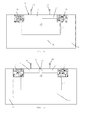
- Figures 7a and 7b illustrate a surface diode structure according to the present invention.
- An active area is an area at and near the surface of a semiconductor substrate where devices (transistors, diodes, etc) are produced. Adjacent active areas are separated by field dielectric regions, for example produced by Shallow Trench Isolation. The width of an active area is the distance between the two field regions between which the active area is located (measured perpendicularly to the edge of the field regions).
- FIG. 1 shows the basic structure of this type of ESD protection device as it is presently known in the art.
- an npn bipolar transistor is formed by n-doped active areas 2 and 3, acting as the emitter and collector of the npn, with the bulk area of the p-substrate acting as the base.
- the first n-doped active area 2 is connected to an ESD terminal 4, which is itself connected to a further n-doped active area 5.
- the second n-doped active area 3 is connected to ground, while the p-substrate is provided with a highly p-doped active area 6, connected to ground via a resistor 7.
- the active areas are separated by field dielectric (usually oxide) regions 11. All regions connected to external contacts are provided with silicide contact areas 15, obtainable by silicidation (e.g. by deposition of Ni and formation of Nickel silicide).
- the p-n junction between the n-doped area 5 and the p-substrate 1 forms a diode 10.
- Region 5 represents the cathode, with region 8 (together with the bulk substrate area 1' and region 6) representing the anode.
- the external terminals of the diode are terminal 4 and the contact 15 to area 6.
- the diode 10 is configured to go into breakdown mode when the ESD terminal 4 receives a high voltage pulse, resulting in a current through the bulk of the substrate and the resistor 7, which triggers the npn into conductive mode in order to divert a high ESD current to ground.
- Area 8 is a highly doped p-implant, the so-called 'ESD implant', considered to be necessary when the p-doping level of substrate 1 is according to standard levels for p-well doping. These levels are such that the breakdown voltage of the diode junction is too high for efficient ESD operation.
- the addition of the ESD implant reduces the breakdown voltage of the diode, which is the holding voltage of the ESD protection device.
- the p-area 6 is obtained by a separate p-implant step at a higher doping level then the substrate, in order to obtain a good ohmic contact from the bulk to the contact area 9.
- Figure 2 illustrates the equivalent circuit of this ESD protection device.
- the present invention reveals a method for producing the structure that allows a reduction in the number of production steps, in particular in the number of steps requiring a mask.
- the invention is equally related to the device as such.
- Figure 3 illustrates the method according to a preferred embodiment.
- the method starts from a Si-substrate 20, possibly a high-resistance Si wafer ( fig. 3a ), possibly a lowly p-doped or undoped substrate.
- the Si-substrate is the Silicon top layer of a Silicon-on-Insulator (SOI) substrate.
- SOI Silicon-on-Insulator
- the substrate may be an interposer substrate for carrying IC's on its surface.
- standard Shallow Trench Isolation (STI) process steps are applied to form field dielectric regions 21, and active areas 23, 24, 25 and 26, each pair of adjacent active areas being separated by a field dielectric region 21 ( figure 3b ).
- STI Shallow Trench Isolation
- the substrate is planarized to form a flat top surface 22 that is common to the active areas and the field dielectric regions 21.
- the substrate area underneath the active areas and the field dielectric regions is referred to hereafter as the substrate bulk area 1'.
- a p-type implant is done ( figure 3c ) in two steps, to obtain a p-doping profile shown in figure 4 .
- the profile shows a highly p-doped region 30 near the surface, exhibiting a maximum p-level at the surface, which gradually decreases at higher depths, a lower-doped region 31 underneath said high-doped region, where the doping level reaches a minimum, and again a more highly doped region 32 in the majority of the bulk area 1' of the substrate 20, where the doping level reaches again a maximum after which it diminishes again to a lower level at still higher depths.
- the second maximum in region 32 is an optional feature, preferably present in certain kinds of devices according to the invention, like the device of figure 3 .
- the first region 30 may have a maximum dopant level of 1E19/cm 3
- the third region 32 may have a minimum dopant level of 2E17/cm 3
- the middle region having a maximum level of 1E16/cm 3 .
- This p-type implant step will hereafter be referred to as a 'graded p-implant'. Further clarification on the characterization of the profile in terms of the separation between the higher and lower doped areas defined by the profile, the preferred ranges for the doping level, and their position with respect to the other components in the structure is given further in this text.
- n-implant step ( figure 3d ), performed through a mask (not shown) according to known practice, for creating the n-doped areas 2 and 3 in active areas 24 and 25, which will serve respectively as the collector and emitter of the bipolar transistor in the ESD protection device, and the n-doped area 5' in active area 23, which is to form the diode at the junction between this n-doped area 5' and the remainder 23' of the active area 23.
- the n-region 5' does not extend over the totality of the width of the active area 23, so that the junction between the n-doped area 5' and said remainder is at least partially formed along the perimeter (i.e. the lateral edge) of the n-doped area 5'.
- a layer of 'pre-metal dielectric' (PMD) 35 is deposited and patterned to form contact holes 36 ( figure 3e ), which are thereafter subjected to a silicidation step and via fill step ( figure 3f ) to form silicide areas 37 and contacts 38.
- the silicidation (as such known in the art, for example by depositing Ni and performing a heating step to form Ni-silicide) thus takes place after deposition of the PMD and formation of the holes 36, which is different from the process for producing the prior art device of figure 1 , where silicidation is done before the contact formation.
- the order of these steps is changed to prevent the active area portion 23' from being subjected to silicidation.
- the ESD protection device is completed by producing the external connections to the terminal 4 and to ground (including resistor 7), in the same way as in the prior art device of figure 1 .
- the characteristic feature of the invention which is the n-implant 5' being formed in only a part of the active area 23, in combination with the graded p-implant, has proven to be advantageous for the following reason.
- the n-implant region 5' exhibits a rounded contact area with the surrounding p-doped area.
- This 'perimeter effect' creates a high electric field locally, which leads to a lower diode breakdown voltage and thus a lower holding voltage for the ESD, without requiring the 'ESD implant' of figure 1 .
- the presence of the p-profile enhances this perimeter effect, due to the local increased p-doping level at the perimeter.
- the holding voltage of the diode in the ESD protection device according to the invention can be tuned by changing the doping level of the p-implant in the region 30 closest to the substrate surface, and hence in the active area portion 23' adjacent to the n-region 5'.
- Figure 6 illustrates the change of the holding voltage from the higher value (in absolute value) of about 10V to the lower value of around 5V when changing from the prior art approach of figure 1 (illustrated by the curve 40) to the approach according to the invention (curves 41 to 43).
- the variation between the curves 41-43 is due to a variation in the p-doping level in area 23'.
- the use of the graded p-implant leading to a higher p-level in the surface region 30 is sufficient for obtaining a desired contact resistance at the p-area 6 in active area 26. No separate p-implant in area 6 is required therefore if the graded p-implant is used.
- Another advantage of the graded p-implant is that the lowest p-doping level is reached in the vicinity of the junction between the n-doped areas 2,3 and the underlying p-doped material. This reduces the junction capacitance of these junctions.
- the higher p-doping level in the bulk of the substrate, in region 32 increases the conductivity of this bulk area, resulting in a more efficient triggering of the ESD protection device.
- the invention is not limited to ESD protection devices as shown in figure 3 , nor to ESD protection devices as such.
- the doping types n and p may be reversed in all of the above detailed description.
- N and P type doping are examples of the 'opposite doping types' referred to elsewhere in this description and in the claims.
- the invention is applicable to other devices than the diode-triggered npn device of figure 3 .
- Figure 7a shows a so-called 'surface diode' according to the invention, with the cathode and anode terminal contacting portions of the same active area 79, located between field dielectric regions 75.
- the p-doped bulk substrate area 1' is itself surrounded by a n-well 78, created in a p-substrate 20.
- the n-doped area 5' is again the cathode of the diode, connected to the cathode terminal 80, with the width of the n-doped area being smaller than the width of the active area 79 wherein it is produced.
- the anode terminal 81 is connected to the remainder of the active area 79.
- Cathode and anode terminals 80/81 are to be understood as including silicidation areas as shown in figure 1 for example. These areas are not drawn in figure 7 for reasons of simplicity.
- a so-called 'surface diode' with the majority of the current flowing in the upper region of the active area.
- the active area and bulk substrate are again provided with the graded p-implant described above, resulting in the upper region 30, which enhances the perimeter effect at the edge of the n-doped region 5' to such a degree that a lower breakdown voltage (in absolute value) is obtained compared to a vertical diode structure (with cathode and anode regions separated by a field dielectric and the cathode covering the complete width of the active area).
- said lower breakdown voltage may be tuned by adapting the doping level in region 30.
- an additional doping implant may be done to obtain an area 6 at the anode terminal for improving the ohmic contact, see embodiment of figure 7b , but this may only be required for specific applications.
- the graded profile does not include the higher doped region 32 in the bulk substrate area 1'. In order to enhance the perimeter effect, it is sufficient that a higher doping level is present near the perimeter of the cathode region 5', i.e. in region 30, then changing to a lower level in region 31, where it stays essentially constant at the bulk doping level at higher depths.
- the doping level changes gradually from a higher to a lower level or vice-versa, preferably according to a Gaussian distribution.
- the minimum level of the profile is reached at a depth that is higher than half the depth of the doped area (5' in the above-described structures) for which the perimeter effect is to be enhanced.
- said minimum is reached at a depth higher than the depth of said doped area 5'.
- the minimum is reached at a depth between half the depth and 1.5 times the depth of said doped area 5'. According to an embodiment, said minimum is reached at or essentially at said depth of said doped area 5'.
- the depth of the area 5' for which the perimeter effect is to be enhanced can be determined as the depth at which a junction appears between said area and the underlying material of opposite doping type.
- Preferred ranges for the maximum doping levels in the profile are the following :
- the upper portion 5' of the active area 23 or 79 is smaller in width than the active area itself, this characteristic is not limited to active areas of constant width as seen in the direction perpendicular to the drawings (i.e. an active area formed between two parallel lines. It is sufficient that the width of the upper portion 5' is smaller than the width of the active area in every cross section of at least a portion of said active area, and in said portion, the width of the active area and of the upper portion 5' may differ from one section to the next, as long as in every one of said sections, the width of the upper portion is smaller than the width of the active area.
- the description of a layer being deposited or produced 'on' another layer or substrate includes the options of
Landscapes
- Semiconductor Integrated Circuits (AREA)
- Bipolar Integrated Circuits (AREA)
- Engineering & Computer Science (AREA)
- Power Engineering (AREA)
Abstract
Description
- The present invention is related to methods for producing a semiconductor device including a diode formed by a junction of differently doped areas in the substrate. The primary application is for the production of Integrated Circuit packages comprising IC's mounted on an interposer chip, provided with Electrostatic Discharge (ESD) protection on the interposer.
- As a cost-reducing measure in IC-packaging, it is known to produce electrostatic discharge protection circuitry on the interposer chip in stead of on the IC's themselves. This is described for example in document
US5644167 and may be referred to as the introduction of an 'active interposer'. An advantage of this approach is that the processing cost of the IC package is reduced. As a larger area is available on the interposer, older CMOS technology manufacturing nodes can be applied on the interposer, leading to a further cost reduction, e.g. 65nm node technology is used on the interposer compared to 32nm node or less on the IC's. - However, the IC-packaging industry continues to look for improvements in terms of cost-effectiveness of the applied processes. ESD protection devices are major examples of semiconductor devices comprising a diode junction. For this type of device, as for others comprising a diode junction, an optimization is needed in terms of the process technology itself, such as the number of process steps and the number of lithography masks applied in the process, in order to further obtain a cost reduction in the production of such devices, for example on an interposer chip,.
- The method and device of the invention provide a way of optimizing the production of a diode structure in a semiconductor device, such as an ESD protection device, making it more cost-effective to produce such devices in general and particularly on an interposer chip. The present invention is related to a semiconductor device comprising a diode junction between two semiconductor regions of different doping types, in particular between an upper portion of an active area and the remainder of said area, said active area being defined in a substrate surface between two field dielectric regions. The upper portion is a portion of the active area that is lower in width than the active area itself. In a preferred embodiment, the device of the invention is an ESD protection device comprising such a diode. In addition, the active area is provided with a doping profile, exhibiting a maximum value at the surface of said active area, and changing to a minimum value at a higher depth, said depth preferably being higher than half the depth of the upper portion. The diode does not require an ESD implant for lowering the holding voltage. As such the device and method according to the invention allow to reduce the number of processing steps in the production of ESD and other devices comprising a diode junction.
- The invention is in particular related to a device and method as disclosed in the appended claims. The invention is firstly related to a semiconductor device comprising a bulk substrate area lying underneath a plurality of field dielectric regions with active area's in between adjacent field dielectric regions, wherein one of said active areas and at least the part of the bulk substrate area underneath said active area is formed of material of a first doping type except for at least one upper portion of said active area that is located between the active area's surface and the depth of said upper portion, said upper portion being formed of material of the doping type opposite to the first doping type, wherein at least in a part of said active area, the width of said upper portion is smaller than the width of the active area, the device comprising a diode in said active area of the device, the diode being formed by at least part of the junction between said upper portion of the active area and the remainder of the active area, the upper portion being connected to a first terminal, the remainder of the active area being connected to a second terminal, and wherein a doping profile of said first doping type is present in said remainder of the active area and the bulk substrate area underneath, said doping profile exhibiting a maximum level at the surface of said active area, wherein the doping level changes to a minimum level at a given depth within said said active area.
- According to one embodiment, said second terminal is connected to the surface of said remainder of the active area. According to another embodiment, said active area is a first active area, and said second terminal is connected to the surface of a second active area (26) of the same doping as said first active area (23).
- According to an embodiment, said profile is such that the doping level again changes to a second maximum value, at a higher depth than said minimum, said second maximum preferably being reached at a depth lying within said bulk substrate area.
- The device of the invention may be an ESD protection device comprising said diode and a bipolar transistor, arranged to conduct current from an ESD terminal to ground after the diode has gone into breakdown mode, the emitter and collector of said transistor being respectively formed by two areas of the same doping type as said upper portion of the (first) active area, said two areas that form the emitter and collector being formed respectively in two further active areas.
- According to an embodiment, said device is located on an interposer substrate on which one or more integrated circuit chips are mounted, said ESD protection device being configured to protect an electrical connection of an IC from electrostatic discharge.
Said semiconductor may be silicon, said upper portion being n-doped and the remainder of said (first) active area being p-doped. - According to an embodiment, said depth at which the minimum doping level is reached is higher than half the depth of said upper portion.
- The invention is also related to a method for producing a semiconductor device comprising a diode, comprising the steps of :
- Providing a semiconductor substrate,
- Creating at least one active area in said substrate, by defining and producing a plurality of field dielectric regions, said active area(s) being located in between two adjacent field dielectric regions,
- producing an area of a first doping type in said substrate, said area comprising said active area(s) and a bulk substrate area lying underneath said active areas and said field dielectric regions,
- Depositing ions of a doping type opposite to said first type, in an upper portion of one of said active areas, said portion being smaller in width than the width of said active area,
- Producing a connection from said upper portion of the active area to a first terminal and a connection from the remainder of said active area to a second terminal, so that a diode is formed by at least part of the junction between said upper portion of the active area and the remainder of said active area,
- According to an embodiment of the method, said second terminal is connected to the surface of said remainder of the active area. According to another embodiment of the method, said active area is a first active area, and said second terminal is connected to the surface of a second active area of the same doping as said first active area.
- According to an embodiment, said profile is such that the doping level again changes to a second maximum value, at a higher depth than said minimum, said second maximum preferably being reached at a depth lying within said bulk substrate area.
- In the method of the invention, said device may be an ESD protection device comprising a diode and a bipolar transistor, the emitter and collector being respectively formed in two further active areas, wherein in said deposition step, ions of said opposite type are deposited in said further active areas to form said emitter and collector.
- According to an embodiment, the step of producing connections from active areas to said terminals comprises a pre-metal dielectric deposition and patterning step to form contact holes, a contact formation step by filling said holes with a contact metal, and a silicidation step for forming silicide areas between the active areas and the contact metal, wherein said silicidation step is performed after the PMD patterning step and before the contact formation step.
- According to an embodiment of the method, said depth at which the minimum doping level is reached is higher than half the depth of said upper portion.
-
Figure 1 illustrates a prior art ESD protection device structure. -
Figure 2 illustrates the electrical equivalent circuit of the device offigure 1 . -
Figures 3a to 3f illustrates the steps of the method according to a preferred embodiment of the invention. -
Figure 4 shows an example of a p-doping profile implanted in the method step illustrated byfigure 3c . -
Figure 5 illustrates the shape of the diode's p-n junction in a device produced according to the invention. -
Figure 6 illustrates the influence of the p-dopant level in the area adjacent to the n-doped area, on the tuning of the ESD protection device's holding voltage. -
Figures 7a and 7b illustrate a surface diode structure according to the present invention. - A few definitions are given which are applicable to certain terminology used in the description. An active area is an area at and near the surface of a semiconductor substrate where devices (transistors, diodes, etc) are produced. Adjacent active areas are separated by field dielectric regions, for example produced by Shallow Trench Isolation. The width of an active area is the distance between the two field regions between which the active area is located (measured perpendicularly to the edge of the field regions).
- By way of example, the structure and fabrication method is hereafter described of an ESD protection device known as a 'diode-triggered npn'. The structure of such a device as known in the art is described and then compared to the structure and its fabrication method according to the invention.
Figure 1 shows the basic structure of this type of ESD protection device as it is presently known in the art. In a p-doped silicon substrate 1 (this may be a p-well created in a lowly doped or undoped Si-substrate, or in an n-well itself created in a p-well or p-substrate), an npn bipolar transistor is formed by n-dopedactive areas active area 2 is connected to an ESD terminal 4, which is itself connected to a further n-dopedactive area 5. The second n-dopedactive area 3 is connected to ground, while the p-substrate is provided with a highly p-dopedactive area 6, connected to ground via aresistor 7. The active areas are separated by field dielectric (usually oxide)regions 11. All regions connected to external contacts are provided withsilicide contact areas 15, obtainable by silicidation (e.g. by deposition of Ni and formation of Nickel silicide). - The p-n junction between the n-doped
area 5 and the p-substrate 1 forms adiode 10.Region 5 represents the cathode, with region 8 (together with the bulk substrate area 1' and region 6) representing the anode. The external terminals of the diode are terminal 4 and thecontact 15 toarea 6. Thediode 10 is configured to go into breakdown mode when the ESD terminal 4 receives a high voltage pulse, resulting in a current through the bulk of the substrate and theresistor 7, which triggers the npn into conductive mode in order to divert a high ESD current to ground.Area 8 is a highly doped p-implant, the so-called 'ESD implant', considered to be necessary when the p-doping level ofsubstrate 1 is according to standard levels for p-well doping. These levels are such that the breakdown voltage of the diode junction is too high for efficient ESD operation. The addition of the ESD implant reduces the breakdown voltage of the diode, which is the holding voltage of the ESD protection device. The p-area 6 is obtained by a separate p-implant step at a higher doping level then the substrate, in order to obtain a good ohmic contact from the bulk to the contact area 9.Figure 2 illustrates the equivalent circuit of this ESD protection device. - This structure as such is known in the art. The present invention reveals a method for producing the structure that allows a reduction in the number of production steps, in particular in the number of steps requiring a mask. The invention is equally related to the device as such.
-
Figure 3 illustrates the method according to a preferred embodiment. The method starts from a Si-substrate 20, possibly a high-resistance Si wafer (fig. 3a ), possibly a lowly p-doped or undoped substrate. According to a preferred embodiment, the Si-substrate is the Silicon top layer of a Silicon-on-Insulator (SOI) substrate. The substrate may be an interposer substrate for carrying IC's on its surface. In the next step, standard Shallow Trench Isolation (STI) process steps are applied to form fielddielectric regions 21, andactive areas figure 3b ). The substrate is planarized to form a flattop surface 22 that is common to the active areas and the fielddielectric regions 21. The substrate area underneath the active areas and the field dielectric regions is referred to hereafter as the substrate bulk area 1'. Then a p-type implant is done (figure 3c ) in two steps, to obtain a p-doping profile shown infigure 4 . The profile shows a highly p-dopedregion 30 near the surface, exhibiting a maximum p-level at the surface, which gradually decreases at higher depths, a lower-dopedregion 31 underneath said high-doped region, where the doping level reaches a minimum, and again a more highly dopedregion 32 in the majority of the bulk area 1' of thesubstrate 20, where the doping level reaches again a maximum after which it diminishes again to a lower level at still higher depths. The second maximum inregion 32 is an optional feature, preferably present in certain kinds of devices according to the invention, like the device offigure 3 . By way of example, thefirst region 30 may have a maximum dopant level of 1E19/cm3, thethird region 32 may have a minimum dopant level of 2E17/cm3, with the middle region having a maximum level of 1E16/cm3. This p-type implant step will hereafter be referred to as a 'graded p-implant'. Further clarification on the characterization of the profile in terms of the separation between the higher and lower doped areas defined by the profile, the preferred ranges for the doping level, and their position with respect to the other components in the structure is given further in this text. - This is then followed by an n-implant step (
figure 3d ), performed through a mask (not shown) according to known practice, for creating the n-dopedareas active areas active area 23, which is to form the diode at the junction between this n-doped area 5' and the remainder 23' of theactive area 23. The n-region 5' does not extend over the totality of the width of theactive area 23, so that the junction between the n-doped area 5' and said remainder is at least partially formed along the perimeter (i.e. the lateral edge) of the n-doped area 5'. - After these steps, a layer of 'pre-metal dielectric' (PMD) 35 is deposited and patterned to form contact holes 36 (
figure 3e ), which are thereafter subjected to a silicidation step and via fill step (figure 3f ) to formsilicide areas 37 andcontacts 38. The silicidation (as such known in the art, for example by depositing Ni and performing a heating step to form Ni-silicide) thus takes place after deposition of the PMD and formation of theholes 36, which is different from the process for producing the prior art device offigure 1 , where silicidation is done before the contact formation. In the case of a device according to the invention, the order of these steps is changed to prevent the active area portion 23' from being subjected to silicidation. The ESD protection device is completed by producing the external connections to the terminal 4 and to ground (including resistor 7), in the same way as in the prior art device offigure 1 . - The characteristic feature of the invention, which is the n-implant 5' being formed in only a part of the
active area 23, in combination with the graded p-implant, has proven to be advantageous for the following reason. As shown infigure 5 , the n-implant region 5' exhibits a rounded contact area with the surrounding p-doped area. This 'perimeter effect' creates a high electric field locally, which leads to a lower diode breakdown voltage and thus a lower holding voltage for the ESD, without requiring the 'ESD implant' offigure 1 . The presence of the p-profile enhances this perimeter effect, due to the local increased p-doping level at the perimeter. This approach thus allows to avoid the processing steps related to the ESD implant, thereby reducing the number of masks required in the process, and thus rendering the process more cost-effective. It was further determined that the holding voltage of the diode in the ESD protection device according to the invention can be tuned by changing the doping level of the p-implant in theregion 30 closest to the substrate surface, and hence in the active area portion 23' adjacent to the n-region 5'.Figure 6 illustrates the change of the holding voltage from the higher value (in absolute value) of about 10V to the lower value of around 5V when changing from the prior art approach offigure 1 (illustrated by the curve 40) to the approach according to the invention (curves 41 to 43). The variation between the curves 41-43 is due to a variation in the p-doping level in area 23'. - It was found also that in the case of the diode-triggered npn, the use of the graded p-implant leading to a higher p-level in the
surface region 30 is sufficient for obtaining a desired contact resistance at the p-area 6 inactive area 26. No separate p-implant inarea 6 is required therefore if the graded p-implant is used. Another advantage of the graded p-implant is that the lowest p-doping level is reached in the vicinity of the junction between the n-dopedareas region 32, increases the conductivity of this bulk area, resulting in a more efficient triggering of the ESD protection device. - The invention is not limited to ESD protection devices as shown in
figure 3 , nor to ESD protection devices as such. The doping types n and p may be reversed in all of the above detailed description. N and P type doping are are examples of the 'opposite doping types' referred to elsewhere in this description and in the claims. The invention is applicable to other devices than the diode-triggered npn device offigure 3 .Figure 7a shows a so-called 'surface diode' according to the invention, with the cathode and anode terminal contacting portions of the sameactive area 79, located between fielddielectric regions 75. This is preferably a Zener diode applicable in any type of ESD protection device, wherein the reverse breakdown voltage is tuned through an adequate doping level near the surface of the active area. In this embodiment, the p-doped bulk substrate area 1' is itself surrounded by a n-well 78, created in a p-substrate 20. This is an example of a so-called triple well design, which is however not a requirement in a device according to the invention. The n-doped area 5' is again the cathode of the diode, connected to thecathode terminal 80, with the width of the n-doped area being smaller than the width of theactive area 79 wherein it is produced. Theanode terminal 81 is connected to the remainder of theactive area 79. Cathode andanode terminals 80/81 are to be understood as including silicidation areas as shown infigure 1 for example. These areas are not drawn infigure 7 for reasons of simplicity. - This creates a so-called 'surface diode', with the majority of the current flowing in the upper region of the active area. The active area and bulk substrate are again provided with the graded p-implant described above, resulting in the
upper region 30, which enhances the perimeter effect at the edge of the n-doped region 5' to such a degree that a lower breakdown voltage (in absolute value) is obtained compared to a vertical diode structure (with cathode and anode regions separated by a field dielectric and the cathode covering the complete width of the active area). In addition, said lower breakdown voltage may be tuned by adapting the doping level inregion 30. Possibly, an additional doping implant may be done to obtain anarea 6 at the anode terminal for improving the ohmic contact, see embodiment offigure 7b , but this may only be required for specific applications.
In the structure offigures 7a and 7b , the graded profile does not include the higher dopedregion 32 in the bulk substrate area 1'. In order to enhance the perimeter effect, it is sufficient that a higher doping level is present near the perimeter of the cathode region 5', i.e. inregion 30, then changing to a lower level inregion 31, where it stays essentially constant at the bulk doping level at higher depths. - In any of the above references to a graded doping profile, it must be understood that there is not a sharp line between the various regions of different doping level defined by the profile. As illustrated in
figure 4 , the doping level changes gradually from a higher to a lower level or vice-versa, preferably according to a Gaussian distribution. According to a preferred embodiment, the minimum level of the profile (in region 31) is reached at a depth that is higher than half the depth of the doped area (5' in the above-described structures) for which the perimeter effect is to be enhanced. According to a further embodiment, said minimum is reached at a depth higher than the depth of said doped area 5'. According to another embodiment, the minimum is reached at a depth between half the depth and 1.5 times the depth of said doped area 5'. According to an embodiment, said minimum is reached at or essentially at said depth of said doped area 5'. The depth of the area 5' for which the perimeter effect is to be enhanced can be determined as the depth at which a junction appears between said area and the underlying material of opposite doping type. - Preferred ranges for the maximum doping levels in the profile are the following :
- For the maximum at the surface of the active area (region 30) : between 2E18/cm3 and 4E19/cm3.
- For the minimum in the
region 31 underneath said top region : between 1E16/cm3 and 5E17/cm3. - For the maximum in the third region 32 (if present) : between 1E16/cm3 and 1E18/cm3.
- When it is stated in this description and in the claims that the upper portion 5' of the
active area - While the invention has been illustrated and described in detail in the drawings and foregoing description, such illustration and description are to be considered illustrative or exemplary and not restrictive. Other variations to the disclosed embodiments can be understood and effected by those skilled in the art in practicing the claimed invention, from a study of the drawings, the disclosure and the appended claims. In the claims, the word "comprising" does not exclude other elements or steps, and the indefinite article "a" or "an" does not exclude a plurality. The mere fact that certain measures are recited in mutually different dependent claims does not indicate that a combination of these measures cannot be used to advantage. Any reference signs in the claims should not be construed as limiting the scope.
- The foregoing description details certain embodiments of the invention. It will be appreciated, however, that no matter how detailed the foregoing appears in text, the invention may be practiced in many ways, and is therefore not limited to the embodiments disclosed. It should be noted that the use of particular terminology when describing certain features or aspects of the invention should not be taken to imply that the terminology is being re-defined herein to be restricted to include any specific characteristics of the features or aspects of the invention with which that terminology is associated.
- Unless specifically specified, the description of a layer being deposited or produced 'on' another layer or substrate, includes the options of
- said layer being produced or deposited directly on, i.e. in contact with, said other layer or substrate, and
- said layer being produced on one or a stack of intermediate layers between said layer and said other layer or substrate.
Claims (15)
- A semiconductor device comprising a bulk substrate area (1') lying underneath a plurality of field dielectric regions (21) with active area's in between adjacent field dielectric regions, wherein one of said active areas (23,79) and at least the part of the bulk substrate area underneath said active area is formed of material of a first doping type except for at least one upper portion (5') of said active area that is located between the active area's surface and the depth of said upper portion, said upper portion being formed of material of the doping type opposite to the first doping type, wherein at least in a part of said active area, the width of said upper portion (5') is smaller than the width of the active area (23,79), the device comprising a diode in said active area (23,79) of the device, the diode being formed by at least part of the junction between said upper portion (5') of the active area (23) and the remainder of the active area, the upper portion (5') being connected to a first terminal (4,80), the remainder of the active area being connected to a second terminal, and wherein a doping profile of said first doping type is present in said remainder of the active area and the bulk substrate area underneath, said doping profile exhibiting a maximum level at the surface of said active area, wherein the doping level changes to a minimum level at a given depth within said said active area (23,79).
- Device according to claim 1, wherein said second terminal (81) is connected to the surface of said remainder of the active area.
- Device according to claim 1, wherein said active area (23) is a first active area, and wherein said second terminal is connected to the surface of a second active area (26) of the same doping as said first active area (23).
- Device according to any one of claims 1 to 3, wherein said profile is such that the doping level again changes to a second maximum value, at a higher depth than said minimum, said second maximum preferably being reached at a depth lying within said bulk substrate area (1').
- Device according to claim 4, said device being an ESD protection device comprising said diode and a bipolar transistor, arranged to conduct current from an ESD terminal (4) to ground after the diode has gone into breakdown mode, the emitter and collector of said transistor being respectively formed by two areas (2,3) of the same doping type as said upper portion (5') of the (first) active area (23), said two areas (2,3) that form the emitter and collector being formed respectively in two further active areas (24,25).
- Device according to claim 5, wherein said device is located on an interposer substrate on which one or more integrated circuit chips are mounted, said ESD protection device being configured to protect an electrical connection of an IC from electrostatic discharge.
- Device according to any one of claims 1 to 6, wherein said semiconductor is silicon, said upper portion (5') being n-doped and the remainder of said (first) active area being p-doped.
- Device according to any one of claims 1 to 8, wherein said depth at which the minimum doping level is reached is higher than half the depth of said upper portion (5').
- A method for producing a semiconductor device comprising a diode, comprising the steps of :- Providing a semiconductor substrate (20),- Creating at least one active area (23,79) in said substrate, by defining and producing a plurality of field dielectric regions (21,75), said active area(s) being located in between two adjacent field dielectric regions,- producing an area of a first doping type in said substrate, said area comprising said active area(s) (23,79) and a bulk substrate area (1') lying underneath said active areas and said field dielectric regions,- Depositing ions of a doping type opposite to said first type, in an upper portion (5') of one of said active areas (23), said portion being smaller in width than the width of said active area (23),- Producing a connection from said upper portion (5') of the active area to a first terminal (4,80) and a connection from the remainder of said active area to a second terminal (81), so that a diode is formed by at least part of the junction between said upper portion (5') of the active area and the remainder of said active area (23),
wherein the step of producing said area of a first doping type comprises implanting the substrate with dopants of said first type, so that a doping profile is created in said active area and the bulk substrate area underneath it, said doping profile exhibiting a maximum level at the surface of said active area, and wherein the doping level changes to a minimum level at a given depth within said said active area (23,79). - Method according to claim 9, wherein said second terminal (81) is connected to the surface of said remainder of the active area (79).
- Method according to claim 9, wherein said active area (23) is a first active area, and wherein said second terminal is connected to the surface of a second active area (26) of the same doping as said first active area (23).
- Method according to any one of claims 9 to 11, wherein said profile is such that the doping level again changes to a second maximum value, at a higher depth than said minimum, said second maximum preferably being reached at a depth lying within said bulk substrate area (1').
- Method according to claim 12 wherein said device is an ESD protection device comprising a diode (10) and a bipolar transistor, the emitter and collector (2,3) being respectively formed in two further active areas (24,25), wherein in said deposition step, ions of said opposite type are deposited in said further active areas (24,25) to form said emitter and collector.
- Method according to any one of claims 9 to 13, wherein the step of producing connections from active areas to said terminals comprises a pre-metal dielectric (35) deposition and patterning step to form contact holes (36), a contact formation step by filling said holes with a contact metal, and a silicidation step for forming silicide areas between the active areas and the contact metal, wherein said silicidation step is performed after the PMD patterning step and before the contact formation step.
- Method according to any one of claims 9 to 14, wherein said depth at which the minimum doping level is reached is higher than half the depth of said upper portion (5').
Priority Applications (2)
| Application Number | Priority Date | Filing Date | Title |
|---|---|---|---|
| EP12190455.1A EP2725615B1 (en) | 2012-10-29 | 2012-10-29 | Semiconductor device comprising a diode and a bipolar transistor and method for producing such a device |
| US14/066,545 US9263401B2 (en) | 2012-10-29 | 2013-10-29 | Semiconductor device comprising a diode and a method for producing such a device |
Applications Claiming Priority (1)
| Application Number | Priority Date | Filing Date | Title |
|---|---|---|---|
| EP12190455.1A EP2725615B1 (en) | 2012-10-29 | 2012-10-29 | Semiconductor device comprising a diode and a bipolar transistor and method for producing such a device |
Publications (2)
| Publication Number | Publication Date |
|---|---|
| EP2725615A1 true EP2725615A1 (en) | 2014-04-30 |
| EP2725615B1 EP2725615B1 (en) | 2019-01-23 |
Family
ID=47263078
Family Applications (1)
| Application Number | Title | Priority Date | Filing Date |
|---|---|---|---|
| EP12190455.1A Active EP2725615B1 (en) | 2012-10-29 | 2012-10-29 | Semiconductor device comprising a diode and a bipolar transistor and method for producing such a device |
Country Status (2)
| Country | Link |
|---|---|
| US (1) | US9263401B2 (en) |
| EP (1) | EP2725615B1 (en) |
Families Citing this family (2)
| Publication number | Priority date | Publication date | Assignee | Title |
|---|---|---|---|---|
| US11855074B2 (en) * | 2021-02-08 | 2023-12-26 | Globalfoundries U.S. Inc. | Electrostatic discharge devices |
| US11756953B2 (en) * | 2021-03-05 | 2023-09-12 | Taiwan Semiconductor Manufacturing Company, Ltd. | Electrostatic discharge protection device |
Citations (3)
| Publication number | Priority date | Publication date | Assignee | Title |
|---|---|---|---|---|
| EP0426241A2 (en) * | 1989-10-31 | 1991-05-08 | STMicroelectronics S.r.l. | Process for the manufacture of a component to limit the programming voltage and to stabilise the voltage incorporated in an electric device with EEPROM memory cells |
| US5644167A (en) | 1996-03-01 | 1997-07-01 | National Semiconductor Corporation | Integrated circuit package assemblies including an electrostatic discharge interposer |
| EP1355363A2 (en) * | 2002-04-18 | 2003-10-22 | Matsushita Electric Industrial Co., Ltd. | Semiconductor device and method for fabricating the same |
Family Cites Families (6)
| Publication number | Priority date | Publication date | Assignee | Title |
|---|---|---|---|---|
| US6586317B1 (en) | 2001-05-08 | 2003-07-01 | National Semiconductor Corporation | Method of forming a zener diode in a npn and pnp bipolar process flow that requires no additional steps to set the breakdown voltage |
| US7119401B2 (en) | 2004-01-07 | 2006-10-10 | International Business Machines Corporation | Tunable semiconductor diodes |
| ATE518249T1 (en) | 2004-04-22 | 2011-08-15 | Ibm | TUNABLE SEMICONDUCTOR COMPONENT |
| JP2006128293A (en) * | 2004-10-27 | 2006-05-18 | Matsushita Electric Ind Co Ltd | Electrostatic protection element of semiconductor integrated circuit |
| US7781826B2 (en) * | 2006-11-16 | 2010-08-24 | Alpha & Omega Semiconductor, Ltd. | Circuit configuration and manufacturing processes for vertical transient voltage suppressor (TVS) and EMI filter |
| US7538395B2 (en) | 2007-09-21 | 2009-05-26 | Semiconductor Components Industries, L.L.C. | Method of forming low capacitance ESD device and structure therefor |
-
2012
- 2012-10-29 EP EP12190455.1A patent/EP2725615B1/en active Active
-
2013
- 2013-10-29 US US14/066,545 patent/US9263401B2/en active Active
Patent Citations (3)
| Publication number | Priority date | Publication date | Assignee | Title |
|---|---|---|---|---|
| EP0426241A2 (en) * | 1989-10-31 | 1991-05-08 | STMicroelectronics S.r.l. | Process for the manufacture of a component to limit the programming voltage and to stabilise the voltage incorporated in an electric device with EEPROM memory cells |
| US5644167A (en) | 1996-03-01 | 1997-07-01 | National Semiconductor Corporation | Integrated circuit package assemblies including an electrostatic discharge interposer |
| EP1355363A2 (en) * | 2002-04-18 | 2003-10-22 | Matsushita Electric Industrial Co., Ltd. | Semiconductor device and method for fabricating the same |
Non-Patent Citations (2)
| Title |
|---|
| SEMENOV O ET AL: "ESD protection design for I/O libraries in advanced CMOS technologies", SOLID STATE ELECTRONICS, ELSEVIER SCIENCE PUBLISHERS, BARKING, GB, vol. 52, no. 8, 1 August 2008 (2008-08-01), pages 1127 - 1139, XP023612438, ISSN: 0038-1101, [retrieved on 20080627], DOI: 10.1016/J.SSE.2008.05.008 * |
| WEN-YI CHEN ET AL: "Diode-Triggered Silicon-Controlled Rectifier With Reduced Voltage Overshoot for CDM ESD Protection", IEEE TRANSACTIONS ON DEVICE AND MATERIALS RELIABILITY, IEEE SERVICE CENTER, PISCATAWAY, NJ, US, vol. 12, no. 1, 1 March 2012 (2012-03-01), pages 10 - 14, XP011429267, ISSN: 1530-4388, DOI: 10.1109/TDMR.2011.2171487 * |
Also Published As
| Publication number | Publication date |
|---|---|
| US9263401B2 (en) | 2016-02-16 |
| US20140124894A1 (en) | 2014-05-08 |
| EP2725615B1 (en) | 2019-01-23 |
Similar Documents
| Publication | Publication Date | Title |
|---|---|---|
| US11869933B2 (en) | Device isolator with reduced parasitic capacitance | |
| US8377757B2 (en) | Device and method for transient voltage suppressor | |
| US11521961B2 (en) | Back ballasted vertical NPN transistor | |
| US11233045B2 (en) | Transient voltage suppression device and manufacturing method therefor | |
| TWI610347B (en) | Production of multiple semiconductor devices using a semiconductor process | |
| US10672758B2 (en) | Electrostatic discharge protection structure, method for manufacturing an electrostatic discharge protection structure, and vertical thyristor structure | |
| US8946041B2 (en) | Methods for forming high gain tunable bipolar transistors | |
| US9991350B2 (en) | Low resistance sinker contact | |
| US10629715B2 (en) | Unidirectional ESD protection with buried breakdown thyristor device | |
| US9716187B2 (en) | Trench semiconductor device having multiple trench depths and method | |
| US11049853B2 (en) | ESD protection device with breakdown voltage stabilization | |
| US8722475B2 (en) | Method and structure for high Q varactor | |
| US9831327B2 (en) | Electrostatic discharge protection devices and methods of forming the same | |
| EP2725615B1 (en) | Semiconductor device comprising a diode and a bipolar transistor and method for producing such a device | |
| US9281304B2 (en) | Transistor assisted ESD diode | |
| US8563387B2 (en) | Transistor and method of manufacturing a transistor | |
| EP1653518A2 (en) | Method of manufacturing a Zener zap diode compatible with tungsten plug technology | |
| US10868198B2 (en) | Semiconductor device including zener diode and method of manufacturing thereof | |
| US6894318B2 (en) | Diode having a double implanted guard ring | |
| KR101779588B1 (en) | Transient voltage suppressor and manufacturing method thereof | |
| CN100446276C (en) | Punch-through diode and method for manufacturing the same | |
| US20240194668A1 (en) | Electrostatic discharge protection structure | |
| CN119153330A (en) | Semiconductor device and method for manufacturing the same | |
| US20160163659A1 (en) | Radio frequency device protected against overvoltages |
Legal Events
| Date | Code | Title | Description |
|---|---|---|---|
| PUAI | Public reference made under article 153(3) epc to a published international application that has entered the european phase |
Free format text: ORIGINAL CODE: 0009012 |
|
| 17P | Request for examination filed |
Effective date: 20121029 |
|
| AK | Designated contracting states |
Kind code of ref document: A1 Designated state(s): AL AT BE BG CH CY CZ DE DK EE ES FI FR GB GR HR HU IE IS IT LI LT LU LV MC MK MT NL NO PL PT RO RS SE SI SK SM TR |
|
| AX | Request for extension of the european patent |
Extension state: BA ME |
|
| 17P | Request for examination filed |
Effective date: 20141020 |
|
| RBV | Designated contracting states (corrected) |
Designated state(s): AL AT BE BG CH CY CZ DE DK EE ES FI FR GB GR HR HU IE IS IT LI LT LU LV MC MK MT NL NO PL PT RO RS SE SI SK SM TR |
|
| STAA | Information on the status of an ep patent application or granted ep patent |
Free format text: STATUS: EXAMINATION IS IN PROGRESS |
|
| 17Q | First examination report despatched |
Effective date: 20161222 |
|
| RAP1 | Party data changed (applicant data changed or rights of an application transferred) |
Owner name: IMEC VZW |
|
| GRAP | Despatch of communication of intention to grant a patent |
Free format text: ORIGINAL CODE: EPIDOSNIGR1 |
|
| STAA | Information on the status of an ep patent application or granted ep patent |
Free format text: STATUS: GRANT OF PATENT IS INTENDED |
|
| INTG | Intention to grant announced |
Effective date: 20180810 |
|
| GRAS | Grant fee paid |
Free format text: ORIGINAL CODE: EPIDOSNIGR3 |
|
| GRAA | (expected) grant |
Free format text: ORIGINAL CODE: 0009210 |
|
| STAA | Information on the status of an ep patent application or granted ep patent |
Free format text: STATUS: THE PATENT HAS BEEN GRANTED |
|
| AK | Designated contracting states |
Kind code of ref document: B1 Designated state(s): AL AT BE BG CH CY CZ DE DK EE ES FI FR GB GR HR HU IE IS IT LI LT LU LV MC MK MT NL NO PL PT RO RS SE SI SK SM TR |
|
| REG | Reference to a national code |
Ref country code: GB Ref legal event code: FG4D |
|
| REG | Reference to a national code |
Ref country code: CH Ref legal event code: EP |
|
| REG | Reference to a national code |
Ref country code: AT Ref legal event code: REF Ref document number: 1092134 Country of ref document: AT Kind code of ref document: T Effective date: 20190215 |
|
| REG | Reference to a national code |
Ref country code: IE Ref legal event code: FG4D |
|
| REG | Reference to a national code |
Ref country code: DE Ref legal event code: R096 Ref document number: 602012056163 Country of ref document: DE |
|
| REG | Reference to a national code |
Ref country code: NL Ref legal event code: MP Effective date: 20190123 |
|
| PG25 | Lapsed in a contracting state [announced via postgrant information from national office to epo] |
Ref country code: NL Free format text: LAPSE BECAUSE OF FAILURE TO SUBMIT A TRANSLATION OF THE DESCRIPTION OR TO PAY THE FEE WITHIN THE PRESCRIBED TIME-LIMIT Effective date: 20190123 |
|
| PG25 | Lapsed in a contracting state [announced via postgrant information from national office to epo] |
Ref country code: SE Free format text: LAPSE BECAUSE OF FAILURE TO SUBMIT A TRANSLATION OF THE DESCRIPTION OR TO PAY THE FEE WITHIN THE PRESCRIBED TIME-LIMIT Effective date: 20190123 Ref country code: PT Free format text: LAPSE BECAUSE OF FAILURE TO SUBMIT A TRANSLATION OF THE DESCRIPTION OR TO PAY THE FEE WITHIN THE PRESCRIBED TIME-LIMIT Effective date: 20190523 Ref country code: FI Free format text: LAPSE BECAUSE OF FAILURE TO SUBMIT A TRANSLATION OF THE DESCRIPTION OR TO PAY THE FEE WITHIN THE PRESCRIBED TIME-LIMIT Effective date: 20190123 Ref country code: NO Free format text: LAPSE BECAUSE OF FAILURE TO SUBMIT A TRANSLATION OF THE DESCRIPTION OR TO PAY THE FEE WITHIN THE PRESCRIBED TIME-LIMIT Effective date: 20190423 Ref country code: PL Free format text: LAPSE BECAUSE OF FAILURE TO SUBMIT A TRANSLATION OF THE DESCRIPTION OR TO PAY THE FEE WITHIN THE PRESCRIBED TIME-LIMIT Effective date: 20190123 Ref country code: LT Free format text: LAPSE BECAUSE OF FAILURE TO SUBMIT A TRANSLATION OF THE DESCRIPTION OR TO PAY THE FEE WITHIN THE PRESCRIBED TIME-LIMIT Effective date: 20190123 Ref country code: ES Free format text: LAPSE BECAUSE OF FAILURE TO SUBMIT A TRANSLATION OF THE DESCRIPTION OR TO PAY THE FEE WITHIN THE PRESCRIBED TIME-LIMIT Effective date: 20190123 |
|
| REG | Reference to a national code |
Ref country code: AT Ref legal event code: MK05 Ref document number: 1092134 Country of ref document: AT Kind code of ref document: T Effective date: 20190123 |
|
| PG25 | Lapsed in a contracting state [announced via postgrant information from national office to epo] |
Ref country code: IS Free format text: LAPSE BECAUSE OF FAILURE TO SUBMIT A TRANSLATION OF THE DESCRIPTION OR TO PAY THE FEE WITHIN THE PRESCRIBED TIME-LIMIT Effective date: 20190523 Ref country code: GR Free format text: LAPSE BECAUSE OF FAILURE TO SUBMIT A TRANSLATION OF THE DESCRIPTION OR TO PAY THE FEE WITHIN THE PRESCRIBED TIME-LIMIT Effective date: 20190424 Ref country code: HR Free format text: LAPSE BECAUSE OF FAILURE TO SUBMIT A TRANSLATION OF THE DESCRIPTION OR TO PAY THE FEE WITHIN THE PRESCRIBED TIME-LIMIT Effective date: 20190123 Ref country code: LV Free format text: LAPSE BECAUSE OF FAILURE TO SUBMIT A TRANSLATION OF THE DESCRIPTION OR TO PAY THE FEE WITHIN THE PRESCRIBED TIME-LIMIT Effective date: 20190123 Ref country code: RS Free format text: LAPSE BECAUSE OF FAILURE TO SUBMIT A TRANSLATION OF THE DESCRIPTION OR TO PAY THE FEE WITHIN THE PRESCRIBED TIME-LIMIT Effective date: 20190123 Ref country code: BG Free format text: LAPSE BECAUSE OF FAILURE TO SUBMIT A TRANSLATION OF THE DESCRIPTION OR TO PAY THE FEE WITHIN THE PRESCRIBED TIME-LIMIT Effective date: 20190423 |
|
| REG | Reference to a national code |
Ref country code: DE Ref legal event code: R097 Ref document number: 602012056163 Country of ref document: DE |
|
| PG25 | Lapsed in a contracting state [announced via postgrant information from national office to epo] |
Ref country code: CZ Free format text: LAPSE BECAUSE OF FAILURE TO SUBMIT A TRANSLATION OF THE DESCRIPTION OR TO PAY THE FEE WITHIN THE PRESCRIBED TIME-LIMIT Effective date: 20190123 Ref country code: IT Free format text: LAPSE BECAUSE OF FAILURE TO SUBMIT A TRANSLATION OF THE DESCRIPTION OR TO PAY THE FEE WITHIN THE PRESCRIBED TIME-LIMIT Effective date: 20190123 Ref country code: RO Free format text: LAPSE BECAUSE OF FAILURE TO SUBMIT A TRANSLATION OF THE DESCRIPTION OR TO PAY THE FEE WITHIN THE PRESCRIBED TIME-LIMIT Effective date: 20190123 Ref country code: EE Free format text: LAPSE BECAUSE OF FAILURE TO SUBMIT A TRANSLATION OF THE DESCRIPTION OR TO PAY THE FEE WITHIN THE PRESCRIBED TIME-LIMIT Effective date: 20190123 Ref country code: DK Free format text: LAPSE BECAUSE OF FAILURE TO SUBMIT A TRANSLATION OF THE DESCRIPTION OR TO PAY THE FEE WITHIN THE PRESCRIBED TIME-LIMIT Effective date: 20190123 Ref country code: SK Free format text: LAPSE BECAUSE OF FAILURE TO SUBMIT A TRANSLATION OF THE DESCRIPTION OR TO PAY THE FEE WITHIN THE PRESCRIBED TIME-LIMIT Effective date: 20190123 Ref country code: AL Free format text: LAPSE BECAUSE OF FAILURE TO SUBMIT A TRANSLATION OF THE DESCRIPTION OR TO PAY THE FEE WITHIN THE PRESCRIBED TIME-LIMIT Effective date: 20190123 |
|
| PG25 | Lapsed in a contracting state [announced via postgrant information from national office to epo] |
Ref country code: SM Free format text: LAPSE BECAUSE OF FAILURE TO SUBMIT A TRANSLATION OF THE DESCRIPTION OR TO PAY THE FEE WITHIN THE PRESCRIBED TIME-LIMIT Effective date: 20190123 |
|
| PLBE | No opposition filed within time limit |
Free format text: ORIGINAL CODE: 0009261 |
|
| STAA | Information on the status of an ep patent application or granted ep patent |
Free format text: STATUS: NO OPPOSITION FILED WITHIN TIME LIMIT |
|
| PG25 | Lapsed in a contracting state [announced via postgrant information from national office to epo] |
Ref country code: AT Free format text: LAPSE BECAUSE OF FAILURE TO SUBMIT A TRANSLATION OF THE DESCRIPTION OR TO PAY THE FEE WITHIN THE PRESCRIBED TIME-LIMIT Effective date: 20190123 |
|
| 26N | No opposition filed |
Effective date: 20191024 |
|
| PG25 | Lapsed in a contracting state [announced via postgrant information from national office to epo] |
Ref country code: SI Free format text: LAPSE BECAUSE OF FAILURE TO SUBMIT A TRANSLATION OF THE DESCRIPTION OR TO PAY THE FEE WITHIN THE PRESCRIBED TIME-LIMIT Effective date: 20190123 |
|
| PG25 | Lapsed in a contracting state [announced via postgrant information from national office to epo] |
Ref country code: TR Free format text: LAPSE BECAUSE OF FAILURE TO SUBMIT A TRANSLATION OF THE DESCRIPTION OR TO PAY THE FEE WITHIN THE PRESCRIBED TIME-LIMIT Effective date: 20190123 |
|
| PG25 | Lapsed in a contracting state [announced via postgrant information from national office to epo] |
Ref country code: MC Free format text: LAPSE BECAUSE OF FAILURE TO SUBMIT A TRANSLATION OF THE DESCRIPTION OR TO PAY THE FEE WITHIN THE PRESCRIBED TIME-LIMIT Effective date: 20190123 |
|
| REG | Reference to a national code |
Ref country code: CH Ref legal event code: PL |
|
| PG25 | Lapsed in a contracting state [announced via postgrant information from national office to epo] |
Ref country code: LI Free format text: LAPSE BECAUSE OF NON-PAYMENT OF DUE FEES Effective date: 20191031 Ref country code: CH Free format text: LAPSE BECAUSE OF NON-PAYMENT OF DUE FEES Effective date: 20191031 Ref country code: LU Free format text: LAPSE BECAUSE OF NON-PAYMENT OF DUE FEES Effective date: 20191029 |
|
| REG | Reference to a national code |
Ref country code: BE Ref legal event code: MM Effective date: 20191031 |
|
| PG25 | Lapsed in a contracting state [announced via postgrant information from national office to epo] |
Ref country code: BE Free format text: LAPSE BECAUSE OF NON-PAYMENT OF DUE FEES Effective date: 20191031 |
|
| GBPC | Gb: european patent ceased through non-payment of renewal fee |
Effective date: 20191029 |
|
| PG25 | Lapsed in a contracting state [announced via postgrant information from national office to epo] |
Ref country code: GB Free format text: LAPSE BECAUSE OF NON-PAYMENT OF DUE FEES Effective date: 20191029 Ref country code: IE Free format text: LAPSE BECAUSE OF NON-PAYMENT OF DUE FEES Effective date: 20191029 |
|
| PG25 | Lapsed in a contracting state [announced via postgrant information from national office to epo] |
Ref country code: CY Free format text: LAPSE BECAUSE OF FAILURE TO SUBMIT A TRANSLATION OF THE DESCRIPTION OR TO PAY THE FEE WITHIN THE PRESCRIBED TIME-LIMIT Effective date: 20190123 |
|
| PG25 | Lapsed in a contracting state [announced via postgrant information from national office to epo] |
Ref country code: HU Free format text: LAPSE BECAUSE OF FAILURE TO SUBMIT A TRANSLATION OF THE DESCRIPTION OR TO PAY THE FEE WITHIN THE PRESCRIBED TIME-LIMIT; INVALID AB INITIO Effective date: 20121029 Ref country code: MT Free format text: LAPSE BECAUSE OF FAILURE TO SUBMIT A TRANSLATION OF THE DESCRIPTION OR TO PAY THE FEE WITHIN THE PRESCRIBED TIME-LIMIT Effective date: 20190123 |
|
| PG25 | Lapsed in a contracting state [announced via postgrant information from national office to epo] |
Ref country code: MK Free format text: LAPSE BECAUSE OF FAILURE TO SUBMIT A TRANSLATION OF THE DESCRIPTION OR TO PAY THE FEE WITHIN THE PRESCRIBED TIME-LIMIT Effective date: 20190123 |
|
| P01 | Opt-out of the competence of the unified patent court (upc) registered |
Effective date: 20230513 |
|
| REG | Reference to a national code |
Ref country code: DE Ref legal event code: R079 Ref document number: 602012056163 Country of ref document: DE Free format text: PREVIOUS MAIN CLASS: H01L0027020000 Ipc: H10D0089000000 |
|
| PGFP | Annual fee paid to national office [announced via postgrant information from national office to epo] |
Ref country code: FR Payment date: 20250925 Year of fee payment: 14 |
|
| PGFP | Annual fee paid to national office [announced via postgrant information from national office to epo] |
Ref country code: DE Payment date: 20250923 Year of fee payment: 14 |