EP2724352B1 - Voltage surge protection device and high voltage circuit breakers - Google Patents
Voltage surge protection device and high voltage circuit breakers Download PDFInfo
- Publication number
- EP2724352B1 EP2724352B1 EP11738409.9A EP11738409A EP2724352B1 EP 2724352 B1 EP2724352 B1 EP 2724352B1 EP 11738409 A EP11738409 A EP 11738409A EP 2724352 B1 EP2724352 B1 EP 2724352B1
- Authority
- EP
- European Patent Office
- Prior art keywords
- protection device
- surge protection
- voltage surge
- varistor
- electrical contact
- Prior art date
- Legal status (The legal status is an assumption and is not a legal conclusion. Google has not performed a legal analysis and makes no representation as to the accuracy of the status listed.)
- Active
Links
Images



Classifications
-
- H—ELECTRICITY
- H01—ELECTRIC ELEMENTS
- H01H—ELECTRIC SWITCHES; RELAYS; SELECTORS; EMERGENCY PROTECTIVE DEVICES
- H01H37/00—Thermally-actuated switches
- H01H37/02—Details
- H01H37/32—Thermally-sensitive members
- H01H37/46—Thermally-sensitive members actuated due to expansion or contraction of a solid
-
- H—ELECTRICITY
- H02—GENERATION; CONVERSION OR DISTRIBUTION OF ELECTRIC POWER
- H02H—EMERGENCY PROTECTIVE CIRCUIT ARRANGEMENTS
- H02H9/00—Emergency protective circuit arrangements for limiting excess current or voltage without disconnection
- H02H9/04—Emergency protective circuit arrangements for limiting excess current or voltage without disconnection responsive to excess voltage
- H02H9/041—Emergency protective circuit arrangements for limiting excess current or voltage without disconnection responsive to excess voltage using a short-circuiting device
-
- H—ELECTRICITY
- H01—ELECTRIC ELEMENTS
- H01C—RESISTORS
- H01C7/00—Non-adjustable resistors formed as one or more layers or coatings; Non-adjustable resistors made from powdered conducting material or powdered semi-conducting material with or without insulating material
- H01C7/10—Non-adjustable resistors formed as one or more layers or coatings; Non-adjustable resistors made from powdered conducting material or powdered semi-conducting material with or without insulating material voltage responsive, i.e. varistors
- H01C7/12—Overvoltage protection resistors; Arresters
-
- H—ELECTRICITY
- H01—ELECTRIC ELEMENTS
- H01H—ELECTRIC SWITCHES; RELAYS; SELECTORS; EMERGENCY PROTECTIVE DEVICES
- H01H37/00—Thermally-actuated switches
- H01H37/74—Switches in which only the opening movement or only the closing movement of a contact is effected by heating or cooling
Definitions
- the invention relates generally to the field of high voltage devices, and in particular to protection of such high voltage devices.
- Voltage dependent resistors are frequently used for protecting electrical devices from voltage surges.
- the varistor is also referred to as non-linear resistor as it has nonlinear current-voltage characteristics. If an applied voltage is less than a certain voltage, the varistor is essentially an insulator. If the voltage applied is above the certain voltage, the switching voltage, the varistor resistance drops and allows an increased current to flow through it.
- the varistor is connected in parallel to the device to be protected and arranged to, when triggered by an overvoltage, shunt the current created by the high voltage away from the device.
- circuit breakers are available for interrupting fault currents. However, it is difficult to design circuit breakers for DC currents due to the high currents without any zero current crossings at which to break the current.
- HVDC high voltage direct current
- IGBT insulated-gate bipolar transistors
- An object of the invention is to provide a voltage surge protection device enabling a safe short-circuit function for high voltage devices, such as circuit breakers.
- the object of the invention is achieved by a voltage surge protection device for protection of a high voltage device according to claim 1.
- the voltage surge protection device comprises a varistor having a first part and a second part, separated by varistor material.
- the voltage surge protection device comprises an expandable member arranged to act on a movable electrical contact for short-circuiting the voltage surge protection device upon a threshold voltage being applied between the first part and the second part of the varistor.
- the invention provides a voltage surge protection device that uses thermal energy of a varistor to trigger a bypass process, whereby neither an external control nor an auxiliary power supply is required to form the bypass.
- the varistor material when subjected to the threshold voltage, produces heat and/or gas expanding the expandable member.
- the movable electrical contact is arranged to be movable between a first position in which the voltage surge protection device is non-activated, and a second position in which the voltage surge protection device is activated.
- the first part and the second part are electrically connected by the movable electrical contact when it is in its second position.
- the varistor comprises an electrically insulating housing enclosing the varistor at least partly in a lengthwise direction of the voltage surge protection device.
- the movable electrical contact is arranged to be movable along the electrically insulating housing between a first position in which the voltage surge protection device is non-activated, and a second position in which the voltage surge protection device is activated, wherein the first part and the second part are electrically connected by the movable electrical contact when it is in its second position.
- the movable electrical contact comprises a movable helical spring or a movable metal ring.
- the voltage surge protection device comprises a movable electrically insulating ring arranged between the expandable member and the electrical contact.
- the expandable member is arranged to act on the movable electrical contact via the movable electrically insulating ring.
- the movable electrically insulating ring may be arranged to be movable along an electrically insulating housing enclosing the varistor at least partly in a lengthwise direction of the voltage surge protection device.
- the movable electrical contact is arranged between the expandable member and an electrically insulating ring.
- the movable electrical contact contacts a helical spring when in the second position, the helical spring being arranged on the lower part.
- the movable electrical contact is arranged in a bore through an electrically insulation housing enclosing the varistor at least partly in a lengthwise direction, and into the varistor material, one side end of the movable electrical contact being in contact with the expandable member arranged as a shell around the varistor material and partly in the bore, the movable electrical contact being arranged to move in a radial direction.
- the expandable member comprises a material expandable when subjected to temperature rises and/or pressure.
- the expandable member comprises silicone gel, silicone paste or silicone grease.
- a further object of the invention is achieved by a high voltage circuit breaker comprising one or more semiconductor unit(s) connected in series, wherein a voltage surge protection device as above is connected in parallel to each such semiconductor unit(s), according to claim 11.
- a further object of the invention is achieved by a high voltage circuit breaker comprising two or more semiconductor units, wherein the semiconductor units are connected anti-serially pairwise, and wherein a voltage surge protection device as above is connected in parallel to each such pair of semiconductor units, according to claim 12.
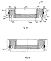
- FIGs 1a and 1b illustrate a voltage surge protection device in accordance with a first embodiment of the invention, before and after activation thereof.
- the voltage surge protection device 1 in the following denoted protection device 1, is illustrated in figure 1a in a cross-sectional view before activation.
- the voltage surge protection device 1 is suitable for protecting high voltage devices, high voltage direct current devices as well as high voltage alternating current devices.
- the protection device 1 comprises a varistor 2 having a sealed insulating housing 3 preferably of a cylindrical shape.
- the varistor 2 comprises a first part 2a, in the following denoted upper part 2a, and a second part 2b, in the following denoted lower part 2b.
- the upper and lower parts 2a, 2b are made of metal and constitute electrodes.
- the upper part 2a and the lower part 2b are separated by varistor material 4.
- the varistor 2 may for example be a metal oxide varistor (MOV).
- MOV metal oxide varistor
- the varistor material 4 and the upper part 2a of the varistor 2 are surrounded, circumferentially and in the length direction L, by an expandable member 5.
- the expandable member 5 is thus arranged, in a radial direction r of the protection device 1, between at least part of the surrounding cylindrical insulating housing 3 on one side and the varistor material 4 and the upper part 2a of the varistor 2 on another side.
- the expandable member 5 comprises a material having a voltage withstand exceeding the protective level of the varistor 2.
- the expandable member 5 is thermally, chemically and electrically stable prior to varistor 2 failure and is chosen so as to withstand temperatures that appears when the varistor 2 absorbs its rated energy, for example 250°C. The heat generated by the varistor material 4 upon failure of the varistor 2 is quickly and efficiently transferred to the expandable member 5.
- the expandable member 5 Upon failure of the varistor 2, defined for example by a varistor temperature exceeding 300°C or by arcing occurring inside or along a collar of the varistor 2, the expandable member 5 breaks down thermally, thereby producing gases through chemical decomposition.
- the expandable member 5 surrounding the varistor material 4 has a viscosity that enables a gas pressure to activate an electrical contact device, which will be described more in detail later.
- the upper part 2a of the varistor 2 is designed so as to comprise, at a radial distance from the center of the protection device 1, a ring shaped first channel 8 having a suitable first width w1* and being partly filled.
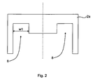
- the first channel 8 is illustrated separately in figure 2 for clarity, and it can be seen in figures 1a and 1b that the expandable member 5 is arranged in the first channel.
- a movable insulating ring 6 is arranged as a collar around the insulating housing 3.
- the insulating ring 6 is movable between a first and a second position in the length direction 1 of the protection device 1, i.e. along the insulating housing 3.
- An upper surface of the insulating ring 6 is in contact with the expandable member 5.
- the expandable member 5 is thus surrounded by the upper part 2a of the varistor, the varistor material 4 and the insulating ring 6.
- the insulating housing 3 may have a stepped shape as illustrated in figures 1a and 1b , having at an upper end a projecting part 3a lying on the insulating ring 6.
- the insulating ring 6 has a first position at which parts of its upper surface abuts the projecting part 3a.
- the expandable member 5 surrounds the projecting part 3a of the insulating housing 3.
- the stepped shape of the insulating housing has a lower projecting part 3b surrounded by the lower part 2b of the varistor 2, leaving part of the lower part 2b accessible from a second channel 9.
- a second ring shaped channel 9 is formed in the first channel 8.
- the second channel 9 is formed between the insulating housing 3 and the outermost part of the upper part 2a.
- the second ring shaped channel 9 has a second width w2.
- the lower part 2b of the varistor 2 constitutes, together with the insulating housing 3, a first wall of the second channel 9.
- the outermost part of the upper part 2a of the varistor 2 constitutes an opposite second wall of the second channel 9.
- a movable electrically conductive contact device 7 e.g. a helical spring, is arranged in the second channel 9 .
- the contact device 7 is movable between a first position P1 and a second position P2 in the length direction L of the protection device 1, i.e. partly along the insulating housing 3. In the lengthwise direction L of the protection device 1, the contact device 7 is located below the insulting ring 6.
- the contact device 7 is in the following exemplified by the helical spring for describing the invention, but it is to be noted that the contact device 7 can be any suitable device enabling electrical contact to the made, e.g. a metal ring.
- the helical spring 7 provides a stable short-circuit as it has several contact surfaces with both the upper part 2a and the lower part 2b in the second position P2. Further, the helical spring 7 is easy to put in place, giving a simple manufacture of the protection device 1.
- Figure 1b illustrates the protection device 1 in its activated state.
- the insulating ring 6 is, as mentioned, movable and has an upper position (illustrated at P1 in figure 1a ) in its non-activated state and a lower position P2 (illustrated in figure 1b ) which it takes when the protection device 1 is activated.
- the helical spring 7 is movably arranged below the insulating ring 6 and when the insulating ring 6 is acted on by the expandable member 5, thus moving downwards, also the helical spring 7 is moved downwards.
- the insulating ring 6 and the helical spring 7 are in their upper positions P1, leaving an air clearance between the upper part 2a and the lower part 2b of the varistor 2.
- the air clearance comprises the width w2 of the second channel 9.
- the varistor material 4 produces heat and possibly gases.
- the expandable member 5 then expands due to the increased temperature and gas pressure.
- the expandable member 5 thus acts on the insulating ring 6, which moves the helical spring 7, both then taking their lower positions P2.
- the helical spring 7 In the lower position P2, the helical spring 7 is in electrical contact with the upper part 2a of the varistor 2 and also in electrical contact with the lower part 2b of the varistor 2.
- the helical spring 7 thus short-circuits the protection device 1 by providing electrical contact between the upper part 2a and the lower part 2b.
- FIGS 3a and 3b illustrate a voltage surge protection device 21 in accordance with a second embodiment of the invention, before and after activation thereof.
- the voltage surge protection device 21, in the following protection device 21, is similar to the first embodiment, comprising a varistor 22 having a first part 22a, in the following denoted upper part 22a, and a second part 22b, in the following denoted lower part 22b, separated by varistor material 24.
- the electrical contact 27 comprises a movable metal ring 27 acted on by an expandable member 25, in a similar way as in the above described first embodiment. Only the main differences between the embodiments are described in the following.
- a movable insulating ring 26 is arranged under the metal ring 27 and ensures a required voltage withstand. In a first position P1', when the protection device 21 is non-activated ( figure 3a ) the insulating ring 26 is abutting a helical spring 28 arranged on the lower part 22b.
- the movable metal ring 27 comes in contact with the helical spring 28 arranged on the lower part 22b of the varistor 22.
- the helical spring 28 provides a stable short-circuit as it has several contact surfaces with both the upper part 22a and the lower part 22b.
- the varistor 22 when the varistor 22 fails, heat and gas are produced by the varistor material 24.
- the expandable member 25 then expands and moves due to the increased temperature and gas pressure.
- the expandable member 25 acts on the metal ring 27, which moves to its lower position P2'. In the lower position P2', the metal ring 27 short-circuits the protection device 1 by providing electrical contact between the upper part 22a and the lower part 22b of the varistor 22.
- the voltage surge protection device 1 comprises a movable electrically insulating ring 6 arranged between the expandable member 5, 25 and the electrical contact 7, 27.
- the expandable member 5, 25 is then arranged to act on the movable electrical contact 7, 27 via the movable electrically insulating ring 6.
- the movable electrically insulating ring 6 may be arranged to move along the electrically insulating housing 3, 23.
- the movable electrical contact 7 is arranged between the expandable member 5, 25 and an electrically insulating ring 26.
- the movable electrical contact 7 contacts a helical spring 28 when in the second position P2, P2'.
- the helical spring 28 is then arranged on the lower part 2b, 22b.
- Figure 4 illustrates a feature of an embodiment of the invention.
- the varistor 2, 22 may fail by internal arcing.
- the surfaces in contact with the varistor material 4, 24 can be machined as illustrated in figure 4 . That is, the surfaces comprises protruding parts with a size of a few millimeters thus creating ways for the gas to act on the expandable member 5, 25 while still providing a reliable electrical contact with the varistor 2, 22.
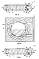
- FIGS 5a, 5b and 5c illustrates yet another embodiment of the voltage surge protection device 1.
- figures 5a and 5b illustrate a voltage surge protection device 31 in accordance with a third embodiment of the invention, before activation thereof
- figure 5c illustrates the voltage surge protection device 31 after activation thereof.
- the voltage surge protection device 31, in the following protection device 31, is similar to the previous embodiments in that it comprises a varistor 32 having a first part 32a, and a second part 32b, separated by varistor material 34.
- a movable electrical contact 37 is arranged to move in a horizontal direction instead of in a vertical direction.
- Figures 5a and 5b illustrate the protection device 31 in a non-activated position, figure 5a in a cross-sectional side view and figure 5b in a cross-sectional top view.
- the expandable member 35 is provided between, as seen in a radial direction, the varistor material 34 and an electrically insulating housing 33. In a vertical direction, the varistor material 34 is provided between the first and second parts 32a, 32b of the varistor 32.
- the expandable member 35 is thus arranged as a cylindrical shell around the varistor material 34, as best seen in figure 5b .
- the movable electrical contact 37 is movably arranged between a first position P1" in which the protection device 31 is non-activated and a second position P2" in which the protection device 31 is activated.
- first position P1 i.e. when the expandable member 35 has not expanded due to gas and pressure from the varistor material 34
- the movable electrical contact 37 is arranged partly through the electrically insulating housing 33 that surrounds the varistor 32, and partly outside the electrically insulating housing 33, thus protruding from the housing 33.
- An end side 39 of the movable electrical contact 37 is in contact with the expandable member 35.
- the movable electrical contact 37 can be seen as arranged in a bore through the electrically insulating housing 33. The bore continues all the way to the shell of expandable member 35, the expandable member 35 thus filling part of this bore, and thereby being in contact with the end side 39 of the movable electrical contact 37.
- the expandable member 35 can thus act on the movable electrical contact 37 upon expansion thereof.
- the expandable member 35 expands and moves the movable electrical contact 37 to its second position P2", in which the first part 32a and the second part 32b are in electrical contact by means of the movable electrical contact 37 moving in a radial direction as mentioned earlier, and thus short-circuiting the protection device 31.
- the movable electrical contact 37 is thus arranged in the bore, through the cylindrical electrically insulation housing 33 that encloses the varistor 32 at least partly in a lengthwise direction.
- the end side of the movable electrical contact 37 is in contact with the expandable member 35 that is arranged as a cylindrical shell around the varistor material 34 and partly in the bore.
- the movable electrical contact 37 is arranged to move in a radial direction, i.e. in a direction perpendicular to the length direction of the protection device 31.
- the protection device 1, 21, 31 comprises a varistor 2, 22, 32 having first part 2a, 22a, 32a and a second part 2b, 22b, 32b, separated by varistor material 4, 24, 34.
- the protection device 1, 21, 31 comprises an expandable member 5, 25, 35 that is arranged to act on a movable electrical contact 7, 27, 37.
- the voltage surge protection device 1, 21, 31 is short-circuited when a threshold voltage is applied between the first part 2a, 22a, 32a and the second part 2b, 22b, 32b of the varistor 2, 22, 32.
- the movable electrical contact 7, 27, 37 is arranged to be movable between a first position P1, P1', P1" in which the voltage surge protection device 1, 21, 31 is non-activated, and a second position P2, P2', P2" in which the voltage surge protection device 1, 21, 31 is activated.
- the varistor and in particular the varistor material 4, 24, 34 In the first position P1, P1', P1' the varistor and in particular the varistor material 4, 24, 34, is essentially electrically non-conducting.
- the second position P2, P2', P2" of the movable electrical contact 7, 27, 37 the first part 2a, 22a, 32a and the second part 2b, 22b, 32b are electrically connected by the movable electrical contact 7, 27, 37.
- the movable electrical contact 7, 27, 37 may be arranged to be movable along an electrically insulating housing 3, 23, 33 that encloses the varistor 2, 22, 32 at least partly in a lengthwise direction L of the protection device 1.
- the movable electrical contact may, for example comprise a movable helical spring 7 or a movable metal ring 27.
- FIG. 6 illustrates a first embodiment of a HVDC circuit breaker comprising a protection device 1, 21, 31 as described.
- the HVDC breaker 40 comprises several series-connected semiconductors, e.g. IGBT units 41 1 , 41 2 ,..., 41 n .
- Each IGBT unit may comprise several parallel-connected IGBT modules.
- One protection device 1, 21, 31 as described is connected in parallel to each such IGBT unit 41 1 , 41 2 ,..., 41 n .
- IGBT units are used here as an example for illustrating and describing the invention, other semiconductor devices can be protected by the inventive concept. Further, yet other switch applications, and even other devices than semiconductor devices, can be protected by protection devices in various aspects of the invention.
- FIG. 7 illustrates a second embodiment of a HVDC circuit breaker comprising a protection device.
- the HVDC circuit breaker 50 of this embodiment also comprises a number of series-connected IGBT units 51 1 , 51 2 , ..., 51 n-1 , 51 n , wherein the IGBT units are connected anti-serially pair-wise, enabling the breaking of current in both current directions.
- One protection device 1, 21, 31 as described is connected in parallel to two such IGBT units.
- the IGBT unit should enter a short-circuit failure mode (SCFM) upon failure.
- SCFM short-circuit failure mode
- the protective device 1, 21, 31 provides such SCFM.
- the protective device 1, 21, 31 changes from the state illustrated in figures 1a and 3a and 5a, 5b to the activated states illustrated in figures 1b and 3b and 5c , as described in relation to these figures.
- the protection device 1, 21, 31 behaves as follows:
- the expandable member 5, 25, 35 should, as mentioned earlier and as is evident from the above, fulfill several requirements.
- the following group of polydimethylesilicone (PDMS) materials has been found to have the electrical, thermal, and viscosity properties required:
- TCDMS tricyclosilicone
- TCDMS 1 mole of TCDMS is created for each mole of PDMS.
- the material consists of 50 % PDMS.
- 50 % of the breakdown products consist of TCDMS. That means that only 25 % of the material is used for gas generation.
- the required layer thickness is estimated for the two embodiments Embodiment 1, Embodiment 2 described in relation to figures 1a, 1b and 3a, 3b , respectively.
- Embodiment Embodiment 1 Embodiment 2 Varistor envelope area cm2 46,6 46,6 46,6 46,6 Helical spring load N 400 400 340 340 Pressure area cm2 40 40 9,2 9,2 Gas pressure on contact ring kPa 200 200 470 470 Expansion volume cm3 68 68 9,2 9,2 Material density g/cm3 1 1 1 1 Gas temperature K 406 673 406 673 Moles of gas 0,00403 0,00243 0,00128 0,00077 Proportion PDMS % 50 50 50 50 50 Proportion TCDMS % 50 50 50 50 units gel/units TCDMS 4 4 4 4 Mole weight TCDMS 222 222 222 222 Mass of gassing material g 3,58 2,16 1,14 0,69 Layer thickness mm 0,77 0,47 0,25 0,15
- the gas temperature is equal to the boiling point of TCDMS (the lowest possible gas temperature).
- the gas temperature is 400° C which is a typical thermal breakdown temperature for the varistor in e.g. HVDC circuit breaker application.
Landscapes
- Engineering & Computer Science (AREA)
- Microelectronics & Electronic Packaging (AREA)
- Physics & Mathematics (AREA)
- Electromagnetism (AREA)
- Thermal Sciences (AREA)
- Emergency Protection Circuit Devices (AREA)
- Thermistors And Varistors (AREA)
Description
- The invention relates generally to the field of high voltage devices, and in particular to protection of such high voltage devices.
- Most electrical systems and devices are occasionally subject to excessive transient voltages being applied and such voltage surges, e.g. due to lightning strikes, may result in very costly damages and subsequent service interruption. Means for protecting the electrical systems and devices are therefore needed.
- Voltage dependent resistors, varistors, are frequently used for protecting electrical devices from voltage surges. The varistor is also referred to as non-linear resistor as it has nonlinear current-voltage characteristics. If an applied voltage is less than a certain voltage, the varistor is essentially an insulator. If the voltage applied is above the certain voltage, the switching voltage, the varistor resistance drops and allows an increased current to flow through it. The varistor is connected in parallel to the device to be protected and arranged to, when triggered by an overvoltage, shunt the current created by the high voltage away from the device.
- Further, various kinds of circuit breakers are available for interrupting fault currents. However, it is difficult to design circuit breakers for DC currents due to the high currents without any zero current crossings at which to break the current.
- One known high voltage direct current (HVDC) circuit breaker based on insulated-gate bipolar transistors (IGBT) technology comprises a number of stack-mounted IGBT units. Each unit comprises several IGBT modules connected in parallel, each module in turn comprising a number of paralleled semiconductor chips which normally carry only a fraction of a line voltage. If one such semiconductor chip (IGBT chip) is destroyed by overvoltage, it is short-circuited by an internal device which has to withstand the full line current. The short-circuiting device has a limited current carrying capability and the complete IGBT unit has to be replaced within short.
- For DC breaker applications, having a large continuous DC current without any zero current crossings which would enhance the transitions from one failed IGBT chip to another, the failed IGBT chip cannot stay in the short circuit mode for very long. The DC breaker thus has to be tripped and the failed device has to be replaced.
- There is thus need for improvements in this regard.
-
DE 102 007 042 989 shows a voltage surge protection device according to the preamble ofclaim 1. - An object of the invention is to provide a voltage surge protection device enabling a safe short-circuit function for high voltage devices, such as circuit breakers.
- The object of the invention is achieved by a voltage surge protection device for protection of a high voltage device according to
claim 1. The voltage surge protection device comprises a varistor having a first part and a second part, separated by varistor material. The voltage surge protection device comprises an expandable member arranged to act on a movable electrical contact for short-circuiting the voltage surge protection device upon a threshold voltage being applied between the first part and the second part of the varistor. The invention provides a voltage surge protection device that uses thermal energy of a varistor to trigger a bypass process, whereby neither an external control nor an auxiliary power supply is required to form the bypass. - The varistor material, when subjected to the threshold voltage, produces heat and/or gas expanding the expandable member.
- In an embodiment, the movable electrical contact is arranged to be movable between a first position in which the voltage surge protection device is non-activated, and a second position in which the voltage surge protection device is activated. The first part and the second part are electrically connected by the movable electrical contact when it is in its second position.
- In an embodiment, the varistor comprises an electrically insulating housing enclosing the varistor at least partly in a lengthwise direction of the voltage surge protection device. The movable electrical contact is arranged to be movable along the electrically insulating housing between a first position in which the voltage surge protection device is non-activated, and a second position in which the voltage surge protection device is activated, wherein the first part and the second part are electrically connected by the movable electrical contact when it is in its second position.
- In an embodiment, the movable electrical contact comprises a movable helical spring or a movable metal ring.
- In an embodiment, the voltage surge protection device comprises a movable electrically insulating ring arranged between the expandable member and the electrical contact. The expandable member is arranged to act on the movable electrical contact via the movable electrically insulating ring. The movable electrically insulating ring may be arranged to be movable along an electrically insulating housing enclosing the varistor at least partly in a lengthwise direction of the voltage surge protection device.
- In an embodiment, the movable electrical contact is arranged between the expandable member and an electrically insulating ring. The movable electrical contact contacts a helical spring when in the second position, the helical spring being arranged on the lower part.
- In an embodiment, the movable electrical contact is arranged in a bore through an electrically insulation housing enclosing the varistor at least partly in a lengthwise direction, and into the varistor material, one side end of the movable electrical contact being in contact with the expandable member arranged as a shell around the varistor material and partly in the bore, the movable electrical contact being arranged to move in a radial direction.
- In an embodiment, the expandable member comprises a material expandable when subjected to temperature rises and/or pressure.
- In an embodiment, the expandable member comprises silicone gel, silicone paste or silicone grease.
- A further object of the invention is achieved by a high voltage circuit breaker comprising one or more semiconductor unit(s) connected in series, wherein a voltage surge protection device as above is connected in parallel to each such semiconductor unit(s), according to claim 11.
- Yet a further object of the invention is achieved by a high voltage circuit breaker comprising two or more semiconductor units, wherein the semiconductor units are connected anti-serially pairwise, and wherein a voltage surge protection device as above is connected in parallel to each such pair of semiconductor units, according to claim 12.
- Further features and advantages thereof will become clear upon reading the following description and the accompanying drawings.
-
-
Figures 1a and 1b illustrate a voltage surge protection device in accordance with a first embodiment of the invention, before and after activation thereof. -
Figure 2 illustrates an upper part of a varistor of the voltage surge protection device offigures 1a and 1b . -
Figures 3a and 3b illustrate a voltage surge protection device in accordance with a second embodiment of the invention, before and after activation thereof. -
Figure 4 illustrates a feature of an embodiment of the invention. -
Figures 5a, 5b and 5c illustrate a voltage surge protection device in accordance with a third embodiment of the invention, in different views before and after activation thereof. -
Figure 6 illustrates a first embodiment of a HVDC circuit breaker comprising a protection device. -
Figure 7 illustrates a second embodiment of a HVDC circuit breaker comprising a protection device. - In the following description, for purposes of explanation and not limitation, specific details are set forth such as particular designs, etc. in order to provide a thorough understanding of the invention. However, it will be apparent to those skilled in the art that the invention may be practiced in other embodiments that depart from these specific details. In other instances, detailed descriptions of well-known devices and circuits are omitted so as not to obscure the description of the invention with unnecessary detail. Like numbers refer to like elements throughout the description.
-
Figures 1a and 1b illustrate a voltage surge protection device in accordance with a first embodiment of the invention, before and after activation thereof. The voltagesurge protection device 1, in the followingdenoted protection device 1, is illustrated infigure 1a in a cross-sectional view before activation. The voltagesurge protection device 1 is suitable for protecting high voltage devices, high voltage direct current devices as well as high voltage alternating current devices. - The
protection device 1 comprises avaristor 2 having a sealedinsulating housing 3 preferably of a cylindrical shape. Thevaristor 2 comprises afirst part 2a, in the following denotedupper part 2a, and asecond part 2b, in the following denotedlower part 2b. The upper andlower parts upper part 2a and thelower part 2b are separated byvaristor material 4. Thevaristor 2 may for example be a metal oxide varistor (MOV). In a length direction L of theprotection device 1, thevaristor 2 thus comprises theupper part 2a, thevaristor material 4 and thelower part 2b. - The
varistor material 4 and theupper part 2a of thevaristor 2 are surrounded, circumferentially and in the length direction L, by anexpandable member 5. Theexpandable member 5 is thus arranged, in a radial direction r of theprotection device 1, between at least part of the surrounding cylindrical insulatinghousing 3 on one side and thevaristor material 4 and theupper part 2a of thevaristor 2 on another side. Theexpandable member 5 comprises a material having a voltage withstand exceeding the protective level of thevaristor 2. Theexpandable member 5 is thermally, chemically and electrically stable prior tovaristor 2 failure and is chosen so as to withstand temperatures that appears when thevaristor 2 absorbs its rated energy, for example 250°C. The heat generated by thevaristor material 4 upon failure of thevaristor 2 is quickly and efficiently transferred to theexpandable member 5. - Upon failure of the
varistor 2, defined for example by a varistor temperature exceeding 300°C or by arcing occurring inside or along a collar of thevaristor 2, theexpandable member 5 breaks down thermally, thereby producing gases through chemical decomposition. Theexpandable member 5 surrounding thevaristor material 4, has a viscosity that enables a gas pressure to activate an electrical contact device, which will be described more in detail later. - The
upper part 2a of thevaristor 2 is designed so as to comprise, at a radial distance from the center of theprotection device 1, a ring shapedfirst channel 8 having a suitable first width w1* and being partly filled. Thefirst channel 8 is illustrated separately infigure 2 for clarity, and it can be seen infigures 1a and 1b that theexpandable member 5 is arranged in the first channel. - A movable
insulating ring 6 is arranged as a collar around the insulatinghousing 3. The insulatingring 6 is movable between a first and a second position in thelength direction 1 of theprotection device 1, i.e. along the insulatinghousing 3. An upper surface of the insulatingring 6 is in contact with theexpandable member 5. Theexpandable member 5 is thus surrounded by theupper part 2a of the varistor, thevaristor material 4 and the insulatingring 6. - The insulating
housing 3 may have a stepped shape as illustrated infigures 1a and 1b , having at an upper end a projectingpart 3a lying on the insulatingring 6. The insulatingring 6 has a first position at which parts of its upper surface abuts the projectingpart 3a. Theexpandable member 5 surrounds the projectingpart 3a of the insulatinghousing 3. The stepped shape of the insulating housing has a lower projectingpart 3b surrounded by thelower part 2b of thevaristor 2, leaving part of thelower part 2b accessible from asecond channel 9. - In the radial direction r, a second ring shaped
channel 9 is formed in thefirst channel 8. Thesecond channel 9 is formed between the insulatinghousing 3 and the outermost part of theupper part 2a. The second ring shapedchannel 9 has a second width w2. Thelower part 2b of thevaristor 2 constitutes, together with the insulatinghousing 3, a first wall of thesecond channel 9. The outermost part of theupper part 2a of thevaristor 2 constitutes an opposite second wall of thesecond channel 9. - In the second channel 9 a movable electrically
conductive contact device 7, e.g. a helical spring, is arranged. Thecontact device 7 is movable between a first position P1 and a second position P2 in the length direction L of theprotection device 1, i.e. partly along the insulatinghousing 3. In the lengthwise direction L of theprotection device 1, thecontact device 7 is located below theinsulting ring 6. Thecontact device 7 is in the following exemplified by the helical spring for describing the invention, but it is to be noted that thecontact device 7 can be any suitable device enabling electrical contact to the made, e.g. a metal ring. Thehelical spring 7 provides a stable short-circuit as it has several contact surfaces with both theupper part 2a and thelower part 2b in the second position P2. Further, thehelical spring 7 is easy to put in place, giving a simple manufacture of theprotection device 1. -
Figure 1b illustrates theprotection device 1 in its activated state. The insulatingring 6 is, as mentioned, movable and has an upper position (illustrated at P1 infigure 1a ) in its non-activated state and a lower position P2 (illustrated infigure 1b ) which it takes when theprotection device 1 is activated. Thehelical spring 7 is movably arranged below the insulatingring 6 and when the insulatingring 6 is acted on by theexpandable member 5, thus moving downwards, also thehelical spring 7 is moved downwards. - In normal operation, illustrated in
figure 1a , the insulatingring 6 and thehelical spring 7 are in their upper positions P1, leaving an air clearance between theupper part 2a and thelower part 2b of thevaristor 2. The air clearance comprises the width w2 of thesecond channel 9. - When the
varistor 2 fails, thevaristor material 4 produces heat and possibly gases. Theexpandable member 5 then expands due to the increased temperature and gas pressure. As mentioned, theexpandable member 5 thus acts on the insulatingring 6, which moves thehelical spring 7, both then taking their lower positions P2. In the lower position P2, thehelical spring 7 is in electrical contact with theupper part 2a of thevaristor 2 and also in electrical contact with thelower part 2b of thevaristor 2. Thehelical spring 7 thus short-circuits theprotection device 1 by providing electrical contact between theupper part 2a and thelower part 2b. -
Figures 3a and 3b illustrate a voltagesurge protection device 21 in accordance with a second embodiment of the invention, before and after activation thereof. The voltagesurge protection device 21, in the followingprotection device 21, is similar to the first embodiment, comprising avaristor 22 having afirst part 22a, in the following denotedupper part 22a, and asecond part 22b, in the following denotedlower part 22b, separated byvaristor material 24. - In the second embodiment, the
electrical contact 27 comprises amovable metal ring 27 acted on by anexpandable member 25, in a similar way as in the above described first embodiment. Only the main differences between the embodiments are described in the following. A movable insulatingring 26 is arranged under themetal ring 27 and ensures a required voltage withstand. In a first position P1', when theprotection device 21 is non-activated (figure 3a ) the insulatingring 26 is abutting ahelical spring 28 arranged on thelower part 22b. - In a second position P2', the
movable metal ring 27 comes in contact with thehelical spring 28 arranged on thelower part 22b of thevaristor 22. Thehelical spring 28 provides a stable short-circuit as it has several contact surfaces with both theupper part 22a and thelower part 22b. - Like in the first embodiment, when the
varistor 22 fails, heat and gas are produced by thevaristor material 24. Theexpandable member 25 then expands and moves due to the increased temperature and gas pressure. Theexpandable member 25 acts on themetal ring 27, which moves to its lower position P2'. In the lower position P2', themetal ring 27 short-circuits theprotection device 1 by providing electrical contact between theupper part 22a and thelower part 22b of thevaristor 22. - In an embodiment, the voltage
surge protection device 1 comprises a movable electrically insulatingring 6 arranged between theexpandable member electrical contact expandable member electrical contact ring 6. The movable electrically insulatingring 6 may be arranged to move along the electrically insulatinghousing - In another embodiment, the movable
electrical contact 7 is arranged between theexpandable member ring 26. The movableelectrical contact 7 contacts ahelical spring 28 when in the second position P2, P2'. Thehelical spring 28 is then arranged on thelower part -
Figure 4 illustrates a feature of an embodiment of the invention. Thevaristor expandable member upper part 2a andlower part 2b of the varistor, the surfaces in contact with thevaristor material figure 4 . That is, the surfaces comprises protruding parts with a size of a few millimeters thus creating ways for the gas to act on theexpandable member varistor -
Figures 5a, 5b and 5c illustrates yet another embodiment of the voltagesurge protection device 1. In particular,figures 5a and 5b illustrate a voltagesurge protection device 31 in accordance with a third embodiment of the invention, before activation thereof, andfigure 5c illustrates the voltagesurge protection device 31 after activation thereof. The voltagesurge protection device 31, in the followingprotection device 31, is similar to the previous embodiments in that it comprises avaristor 32 having afirst part 32a, and asecond part 32b, separated byvaristor material 34. In contrast to the previous embodiments, a movableelectrical contact 37 is arranged to move in a horizontal direction instead of in a vertical direction. -
Figures 5a and 5b illustrate theprotection device 31 in a non-activated position,figure 5a in a cross-sectional side view andfigure 5b in a cross-sectional top view. Theexpandable member 35 is provided between, as seen in a radial direction, thevaristor material 34 and an electrically insulatinghousing 33. In a vertical direction, thevaristor material 34 is provided between the first andsecond parts varistor 32. Theexpandable member 35 is thus arranged as a cylindrical shell around thevaristor material 34, as best seen infigure 5b . - The movable
electrical contact 37 is movably arranged between a first position P1" in which theprotection device 31 is non-activated and a second position P2" in which theprotection device 31 is activated. When in the first position P1", i.e. when theexpandable member 35 has not expanded due to gas and pressure from thevaristor material 34, the movableelectrical contact 37 is arranged partly through the electrically insulatinghousing 33 that surrounds thevaristor 32, and partly outside the electrically insulatinghousing 33, thus protruding from thehousing 33. - An
end side 39 of the movableelectrical contact 37 is in contact with theexpandable member 35. The movableelectrical contact 37 can be seen as arranged in a bore through the electrically insulatinghousing 33. The bore continues all the way to the shell ofexpandable member 35, theexpandable member 35 thus filling part of this bore, and thereby being in contact with theend side 39 of the movableelectrical contact 37. Theexpandable member 35 can thus act on the movableelectrical contact 37 upon expansion thereof. - As for the previously described embodiments, when the
varistor 32 fails, theexpandable member 35 expands and moves the movableelectrical contact 37 to its second position P2", in which thefirst part 32a and thesecond part 32b are in electrical contact by means of the movableelectrical contact 37 moving in a radial direction as mentioned earlier, and thus short-circuiting theprotection device 31. - The movable
electrical contact 37 is thus arranged in the bore, through the cylindricalelectrically insulation housing 33 that encloses thevaristor 32 at least partly in a lengthwise direction. The end side of the movableelectrical contact 37 is in contact with theexpandable member 35 that is arranged as a cylindrical shell around thevaristor material 34 and partly in the bore. The movableelectrical contact 37 is arranged to move in a radial direction, i.e. in a direction perpendicular to the length direction of theprotection device 31. - Three particular embodiments have been described above with reference to
figures 1a, 1b ,2 ,3a, 3b , and5a, 5b, 5c but in its most general embodiment, theprotection device varistor first part second part varistor material protection device expandable member electrical contact surge protection device first part second part varistor - This can be accomplished by the
varistor material expandable member - The movable
electrical contact surge protection device surge protection device varistor material electrical contact first part second part electrical contact - The movable
electrical contact housing varistor protection device 1. - As described earlier, the movable electrical contact may, for example comprise a movable
helical spring 7 or amovable metal ring 27. -
Figure 6 illustrates a first embodiment of a HVDC circuit breaker comprising aprotection device HVDC breaker 40 comprises several series-connected semiconductors,e.g. IGBT units protection device such IGBT unit -
Figure 7 illustrates a second embodiment of a HVDC circuit breaker comprising a protection device. TheHVDC circuit breaker 50 of this embodiment also comprises a number of series-connectedIGBT units protection device - The IGBT unit should enter a short-circuit failure mode (SCFM) upon failure. The
protective device protective device figures 1a and3a and5a, 5b to the activated states illustrated infigures 1b and3b and5c , as described in relation to these figures. - Upon varistor failure, the
protection device - If the varistor temperature exceeds 450-500°C, the
expandable member varistor - The
expandable member electrical contact - The housing shall mechanically withstand the internal gas pressure created by gassing or arcing.
- The
protection device varistor electrical contact - The
expandable member - 1) Silicone gel: two-component, curing at room temperature; very soft (gel hardness <100 g, penetration >5 mm); thermally stable up to +250°C; during heating in oxygen-free environment beginning at about 400°C, the silicone gel is decomposed at into tricyclosilicone (Si(CH3)0)3 and other cyclic low molecular weight silicones.
- 2) Silicone paste: composed of PDMS and thickeners, for example amorphous silica (SiO2); decomposed in a similar way as silicone gel; transfers the hydraulic pressure better that silicone gel
- 3)Silicone grease: composed of silicone oil and a thickener, for example amorphous silica and other fillers; decomposed in a similar way as silicone gel; transfers the hydraulic pressure like silicone paste
- Upon varistor failure, it is most likely that the decomposing of the
expandable member varistor electrical contact varistor block - Theoretically, 1 mole of TCDMS is created for each mole of PDMS. As a conservative assumption the material consists of 50 % PDMS. Suppose also that 50 % of the breakdown products consist of TCDMS. That means that only 25 % of the material is used for gas generation. In the table below, the required layer thickness is estimated for the two
embodiments Embodiment 1,Embodiment 2 described in relation tofigures 1a, 1b and3a, 3b , respectively.Embodiment Embodiment 1 Embodiment 2Varistor envelope area cm2 46,6 46,6 46,6 46,6 Helical spring load N 400 400 340 340 Pressure area cm2 40 40 9,2 9,2 Gas pressure on contact ring kPa 200 200 470 470 Expansion volume cm3 68 68 9,2 9,2 Material density g/ cm3 1 1 1 1 Gas temperature K 406 673 406 673 Moles of gas 0,00403 0,00243 0,00128 0,00077 Proportion PDMS % 50 50 50 50 Proportion TCDMS % 50 50 50 50 units gel/ units TCDMS 4 4 4 4 Mole weight TCDMS 222 222 222 222 Mass of gassing material g 3,58 2,16 1,14 0,69 Layer thickness mm 0,77 0,47 0,25 0,15 - In the left columns of
Embodiment 1 andEmbodiment 2 the gas temperature is equal to the boiling point of TCDMS (the lowest possible gas temperature). In the right columns the gas temperature is 400° C which is a typical thermal breakdown temperature for the varistor in e.g. HVDC circuit breaker application. - These examples show that a very thin layer of gassing material is needed to produce the necessary volume and pressure to activate the contact device in both designs and to ensure that the contact can be pressed all the way until fully closed. It is also shown that the residual gas pressure must be relieved in order to reduce the gas pressure when the contacts have been closed.
Claims (12)
- A voltage surge protection device (1, 21, 31), the voltage surge protection device (1, 21, 31) comprising a varistor (2, 22, 32) having a first part (2a, 22a, 32a) and a second part (2b, 22b, 32b), separated by varistor material (4, 24, 34) configured to produce heat and/or gas when subjected to a threshold voltage applied between the first part (2a, 22a, 32a) and the second part (2b, 22b, 32b) of the varistor (2, 22, 32), whereby an expandable member (5, 25, 35) arranged to act on a movable electrical contact (7, 27, 37) for short-circuiting the voltage surge protection device (1, 21, 31) upon the threshold voltage being applied between the first part (2a, 22a, 32a) and the second part (2b, 22b, 32b) of the varistor (2, 22, 32), characterized by the expandable member (5, 25, 35) is configured to expand due to the heat and/or gas produced by the varistor material (4, 24, 34), the expandable member thereby breaking down thermally and producing gases through chemical decomposition, said gases of the expandable member having a gas pressure that moves the movable electrical contact.
- The voltage surge protection device (1, 21, 31) as claimed in claim 1, wherein the movable electrical contact (7, 27, 37) is arranged to be movable between a first position (P1, P1', P1'') in which the voltage surge protection device (1, 21, 31) is non-activated, and a second position (P2, P2', P2") in which the voltage surge protection device (1, 21, 31) is activated, wherein the first part (2a, 22a, 32a) and the second part (2b, 22b, 32b) are electrically connected by the movable electrical contact (7, 27, 37) when in its second position (P2, P2', P2").
- The voltage surge protection device (1, 21) as claimed in any of the preceding claims, wherein the movable electrical contact comprises a movable helical spring (7) or a movable metal ring (27).
- The voltage surge protection device (1, 21) as claimed in any of the preceding claims, wherein the varistor (2, 22) comprises an electrically insulating housing (3, 23) enclosing the varistor (2, 22) at least partly in a lengthwise direction (1) of the voltage surge protection device (1, 21), and wherein the movable electrical contact (7, 27) is arranged to be movable along the electrically insulating housing (3, 23) between a first position (P1, P1') in which the voltage surge protection device (1, 21) is non-activated, and a second position (P2, P2') in which the voltage surge protection device (1, 21) is activated, wherein the first part (2a, 22a) and the second part (2b, 22b) are electrically connected by the movable electrical contact (7, 27) when in its the second position (P2, P2').
- The voltage surge protection device (1) as claimed in any of the preceding claims, comprising a movable electrically insulating ring (6) arranged between the expandable member (5) and the electrical contact (7), and wherein the expandable member (5) is arranged to act on the movable electrical contact (7) via the movable electrically insulating ring (6).
- The voltage surge protection device (1) as claimed in claim 5, wherein the movable electrically insulating ring (6) is arranged to be movable along an electrically insulating housing (3) enclosing the varistor (2) at least partly in a lengthwise direction (1) of the voltage surge protection device (1).
- The voltage surge protection device (21) as claimed in claim 2 or 4, wherein the movable electrical contact (27) is arranged between the expandable member (25) and an electrically insulating ring (26), and wherein the movable electrical contact (27) contacts a helical spring (28) when in the second position (P2'), the helical spring (28) being arranged on the second part (22b).
- The voltage surge protection device (31) as claimed in any of claims 1-3, wherein the movable electrical contact (37) is arranged in a bore through an electrically insulation housing (33) enclosing the varistor (32) at least partly in a lengthwise direction, one end of the movable electrical contact (37) being in contact with the expandable member (35) arranged as a shell around the varistor material (34) and partly in the bore, the movable electrical contact (37) being arranged to move in a radial direction.
- The voltage surge protection device (1, 21, 31) as claimed in any of the preceding claims, wherein the expandable member (5, 25, 35) comprises a material expandable when subjected to temperature rises and/or pressure.
- The voltage surge protection device (1, 21, 31) as claimed in any of the preceding claims, wherein the expandable member (5, 25, 35) comprises silicone gel, silicone paste or silicone grease.
- A circuit breaker (40) comprising one or more semiconductor unit(s) (411, 412,..., 41n) connected in series, wherein a voltage surge protection device (1, 21, 31) as claimed in any of claims 1-10 is connected in parallel to each such semiconductor unit(s) (411, 412,..., 41n;).
- A circuit breaker (50) comprising two or more semiconductor units (511, 512,..., 51n-1, 51n), wherein the semiconductor units (511, 512, ... 51n-1, 51n) are connected anti-serially pairwise, and wherein a voltage surge protection device (1, 21, 31) as claimed in any of claims 1-10 is connected in parallel to each such pair of semiconductor units (511, 512,..., 51n-1, 51n).
Applications Claiming Priority (1)
| Application Number | Priority Date | Filing Date | Title |
|---|---|---|---|
| PCT/EP2011/060718 WO2013000498A1 (en) | 2011-06-27 | 2011-06-27 | Voltage surge protection device and high voltage circuit breakers |
Publications (2)
| Publication Number | Publication Date |
|---|---|
| EP2724352A1 EP2724352A1 (en) | 2014-04-30 |
| EP2724352B1 true EP2724352B1 (en) | 2015-01-21 |
Family
ID=44629344
Family Applications (1)
| Application Number | Title | Priority Date | Filing Date |
|---|---|---|---|
| EP11738409.9A Active EP2724352B1 (en) | 2011-06-27 | 2011-06-27 | Voltage surge protection device and high voltage circuit breakers |
Country Status (5)
| Country | Link |
|---|---|
| US (1) | US8817445B1 (en) |
| EP (1) | EP2724352B1 (en) |
| KR (1) | KR101436277B1 (en) |
| CN (1) | CN103620704B (en) |
| WO (1) | WO2013000498A1 (en) |
Families Citing this family (3)
| Publication number | Priority date | Publication date | Assignee | Title |
|---|---|---|---|---|
| EP3061111B1 (en) * | 2013-12-20 | 2017-03-29 | Siemens Aktiengesellschaft | Apparatus and method for switching a direct current |
| DE102017118181B4 (en) * | 2017-07-07 | 2019-01-17 | Dehn + Söhne Gmbh + Co. Kg | Encapsulated overvoltage protection device with a cup-like housing |
| DE102023206561A1 (en) * | 2023-07-11 | 2025-01-16 | Siemens Aktiengesellschaft | electronic arrangement |
Family Cites Families (10)
| Publication number | Priority date | Publication date | Assignee | Title |
|---|---|---|---|---|
| DE3318588A1 (en) | 1983-05-21 | 1984-11-22 | Brown, Boveri & Cie Ag, 6800 Mannheim | VARISTOR LOCKING ELEMENT |
| US5583734A (en) | 1994-11-10 | 1996-12-10 | Raychem Corporation | Surge arrester with overvoltage sensitive grounding switch |
| US6304166B1 (en) | 1999-09-22 | 2001-10-16 | Harris Ireland Development Company, Ltd. | Low profile mount for metal oxide varistor package and method |
| SE518070C2 (en) | 2000-12-20 | 2002-08-20 | Abb Ab | VSCconverter |
| US7433169B2 (en) * | 2005-12-15 | 2008-10-07 | Raycap Corporation | Overvoltage protection devices including wafer of varistor material |
| DE102007042989A1 (en) * | 2007-05-29 | 2008-12-04 | Dehn + Söhne Gmbh + Co. Kg | Short-circuiting device for surge arresters |
| ES2378593T3 (en) * | 2008-08-27 | 2012-04-16 | Maschinenfabrik Reinhausen Gmbh | Phase switch with semiconductor switching elements |
| DE102009048045B4 (en) * | 2009-10-02 | 2011-06-01 | Phoenix Contact Gmbh & Co. Kg | Snubber |
| DE102009053145A1 (en) * | 2009-11-05 | 2011-05-12 | Phoenix Contact Gmbh & Co. Kg | Overvoltage protection device, has thermal expandable material arranged within housing such that pole of varistor does not stay in electrically conductive contact with connection elements |
| US8699197B2 (en) * | 2010-08-27 | 2014-04-15 | Cooper Technologies Company | Compact transient voltage surge suppression device |
-
2011
- 2011-06-27 US US14/128,986 patent/US8817445B1/en active Active
- 2011-06-27 CN CN201180071870.2A patent/CN103620704B/en active Active
- 2011-06-27 EP EP11738409.9A patent/EP2724352B1/en active Active
- 2011-06-27 KR KR1020137034632A patent/KR101436277B1/en active Active
- 2011-06-27 WO PCT/EP2011/060718 patent/WO2013000498A1/en not_active Ceased
Also Published As
| Publication number | Publication date |
|---|---|
| US8817445B1 (en) | 2014-08-26 |
| KR20140025544A (en) | 2014-03-04 |
| EP2724352A1 (en) | 2014-04-30 |
| KR101436277B1 (en) | 2014-08-29 |
| CN103620704A (en) | 2014-03-05 |
| WO2013000498A1 (en) | 2013-01-03 |
| CN103620704B (en) | 2016-08-17 |
| US20140226244A1 (en) | 2014-08-14 |
Similar Documents
| Publication | Publication Date | Title |
|---|---|---|
| US12237664B2 (en) | Devices for active overvoltage protection including varistors and thyristors | |
| US8743525B2 (en) | Overvoltage protection devices including wafer of varistor material | |
| CN107533926A (en) | Bypass switch including a movable member having a first conductive portion and a second conductive portion | |
| Xu et al. | SiC based solid state circuit breaker: Thermal design and analysis | |
| CN103262375B (en) | Overvoltage protective discharge device comprising at least one varistor discharge element | |
| Yasuoka et al. | Arcless commutation of a hybrid DC breaker by contact voltage of molten metal bridge | |
| US8817445B1 (en) | Voltage surge protection device and high voltage circuit breakers | |
| EP1681686A1 (en) | PTC current limiting device having molding part made of insulating material | |
| KR102612691B1 (en) | Transient voltage suppression device with thermal blocking | |
| CN110475690B (en) | Voltage limiter with overvoltage protection | |
| CN104658724A (en) | Multi-contact element for a varistor | |
| CN105981242B (en) | Inflate gap | |
| CN217388670U (en) | High-voltage direct-current breaking module and device | |
| KR100697919B1 (en) | PCC current limiter with multiple insulators | |
| CN103400730A (en) | Protection device with over-temperature and over-current double-layer protection function | |
| KR20170046300A (en) | High speed switch using supercritical fluid and current interrupt appratus using it and current interrupt method | |
| EP3358577A1 (en) | Overvoltage protection device including a varistor a fuse and two fail safe mechanisms | |
| KR101194242B1 (en) | Surge protector having preventing thermal runway function | |
| KR100952072B1 (en) | Lightning arrester disconnector | |
| US20170084387A1 (en) | Electrical component | |
| JPH0356030A (en) | Semiconductor type surge protecting apparatus and electronic system connected with the same | |
| KR101977018B1 (en) | Varistor module | |
| CN116996051A (en) | Voltage equalizing method of high-voltage direct-current breaking device, high-voltage direct-current breaking module and device | |
| UA22719U (en) | Non-linear mine switsching excess-voltage suppressor |
Legal Events
| Date | Code | Title | Description |
|---|---|---|---|
| PUAI | Public reference made under article 153(3) epc to a published international application that has entered the european phase |
Free format text: ORIGINAL CODE: 0009012 |
|
| 17P | Request for examination filed |
Effective date: 20140127 |
|
| AK | Designated contracting states |
Kind code of ref document: A1 Designated state(s): AL AT BE BG CH CY CZ DE DK EE ES FI FR GB GR HR HU IE IS IT LI LT LU LV MC MK MT NL NO PL PT RO RS SE SI SK SM TR |
|
| DAX | Request for extension of the european patent (deleted) | ||
| REG | Reference to a national code |
Ref country code: DE Ref legal event code: R079 Ref document number: 602011013343 Country of ref document: DE Free format text: PREVIOUS MAIN CLASS: H01C0007120000 Ipc: H01H0037740000 |
|
| GRAP | Despatch of communication of intention to grant a patent |
Free format text: ORIGINAL CODE: EPIDOSNIGR1 |
|
| RIC1 | Information provided on ipc code assigned before grant |
Ipc: H01C 7/12 20060101ALI20141024BHEP Ipc: H01H 37/74 20060101AFI20141024BHEP Ipc: H02H 9/04 20060101ALI20141024BHEP |
|
| INTG | Intention to grant announced |
Effective date: 20141114 |
|
| GRAS | Grant fee paid |
Free format text: ORIGINAL CODE: EPIDOSNIGR3 |
|
| GRAA | (expected) grant |
Free format text: ORIGINAL CODE: 0009210 |
|
| AK | Designated contracting states |
Kind code of ref document: B1 Designated state(s): AL AT BE BG CH CY CZ DE DK EE ES FI FR GB GR HR HU IE IS IT LI LT LU LV MC MK MT NL NO PL PT RO RS SE SI SK SM TR |
|
| REG | Reference to a national code |
Ref country code: GB Ref legal event code: FG4D |
|
| REG | Reference to a national code |
Ref country code: CH Ref legal event code: EP |
|
| REG | Reference to a national code |
Ref country code: IE Ref legal event code: FG4D |
|
| REG | Reference to a national code |
Ref country code: DE Ref legal event code: R096 Ref document number: 602011013343 Country of ref document: DE Effective date: 20150312 |
|
| REG | Reference to a national code |
Ref country code: AT Ref legal event code: REF Ref document number: 709500 Country of ref document: AT Kind code of ref document: T Effective date: 20150315 |
|
| REG | Reference to a national code |
Ref country code: NL Ref legal event code: VDEP Effective date: 20150121 |
|
| REG | Reference to a national code |
Ref country code: AT Ref legal event code: MK05 Ref document number: 709500 Country of ref document: AT Kind code of ref document: T Effective date: 20150121 |
|
| REG | Reference to a national code |
Ref country code: FR Ref legal event code: PLFP Year of fee payment: 5 |
|
| REG | Reference to a national code |
Ref country code: LT Ref legal event code: MG4D |
|
| PG25 | Lapsed in a contracting state [announced via postgrant information from national office to epo] |
Ref country code: BG Free format text: LAPSE BECAUSE OF FAILURE TO SUBMIT A TRANSLATION OF THE DESCRIPTION OR TO PAY THE FEE WITHIN THE PRESCRIBED TIME-LIMIT Effective date: 20150421 Ref country code: LT Free format text: LAPSE BECAUSE OF FAILURE TO SUBMIT A TRANSLATION OF THE DESCRIPTION OR TO PAY THE FEE WITHIN THE PRESCRIBED TIME-LIMIT Effective date: 20150121 Ref country code: SE Free format text: LAPSE BECAUSE OF FAILURE TO SUBMIT A TRANSLATION OF THE DESCRIPTION OR TO PAY THE FEE WITHIN THE PRESCRIBED TIME-LIMIT Effective date: 20150121 Ref country code: NO Free format text: LAPSE BECAUSE OF FAILURE TO SUBMIT A TRANSLATION OF THE DESCRIPTION OR TO PAY THE FEE WITHIN THE PRESCRIBED TIME-LIMIT Effective date: 20150421 Ref country code: FI Free format text: LAPSE BECAUSE OF FAILURE TO SUBMIT A TRANSLATION OF THE DESCRIPTION OR TO PAY THE FEE WITHIN THE PRESCRIBED TIME-LIMIT Effective date: 20150121 Ref country code: ES Free format text: LAPSE BECAUSE OF FAILURE TO SUBMIT A TRANSLATION OF THE DESCRIPTION OR TO PAY THE FEE WITHIN THE PRESCRIBED TIME-LIMIT Effective date: 20150121 Ref country code: HR Free format text: LAPSE BECAUSE OF FAILURE TO SUBMIT A TRANSLATION OF THE DESCRIPTION OR TO PAY THE FEE WITHIN THE PRESCRIBED TIME-LIMIT Effective date: 20150121 |
|
| PG25 | Lapsed in a contracting state [announced via postgrant information from national office to epo] |
Ref country code: GR Free format text: LAPSE BECAUSE OF FAILURE TO SUBMIT A TRANSLATION OF THE DESCRIPTION OR TO PAY THE FEE WITHIN THE PRESCRIBED TIME-LIMIT Effective date: 20150422 Ref country code: IS Free format text: LAPSE BECAUSE OF FAILURE TO SUBMIT A TRANSLATION OF THE DESCRIPTION OR TO PAY THE FEE WITHIN THE PRESCRIBED TIME-LIMIT Effective date: 20150521 Ref country code: AT Free format text: LAPSE BECAUSE OF FAILURE TO SUBMIT A TRANSLATION OF THE DESCRIPTION OR TO PAY THE FEE WITHIN THE PRESCRIBED TIME-LIMIT Effective date: 20150121 Ref country code: NL Free format text: LAPSE BECAUSE OF FAILURE TO SUBMIT A TRANSLATION OF THE DESCRIPTION OR TO PAY THE FEE WITHIN THE PRESCRIBED TIME-LIMIT Effective date: 20150121 Ref country code: RS Free format text: LAPSE BECAUSE OF FAILURE TO SUBMIT A TRANSLATION OF THE DESCRIPTION OR TO PAY THE FEE WITHIN THE PRESCRIBED TIME-LIMIT Effective date: 20150121 Ref country code: LV Free format text: LAPSE BECAUSE OF FAILURE TO SUBMIT A TRANSLATION OF THE DESCRIPTION OR TO PAY THE FEE WITHIN THE PRESCRIBED TIME-LIMIT Effective date: 20150121 Ref country code: PL Free format text: LAPSE BECAUSE OF FAILURE TO SUBMIT A TRANSLATION OF THE DESCRIPTION OR TO PAY THE FEE WITHIN THE PRESCRIBED TIME-LIMIT Effective date: 20150121 |
|
| REG | Reference to a national code |
Ref country code: DE Ref legal event code: R097 Ref document number: 602011013343 Country of ref document: DE |
|
| PG25 | Lapsed in a contracting state [announced via postgrant information from national office to epo] |
Ref country code: EE Free format text: LAPSE BECAUSE OF FAILURE TO SUBMIT A TRANSLATION OF THE DESCRIPTION OR TO PAY THE FEE WITHIN THE PRESCRIBED TIME-LIMIT Effective date: 20150121 Ref country code: RO Free format text: LAPSE BECAUSE OF FAILURE TO SUBMIT A TRANSLATION OF THE DESCRIPTION OR TO PAY THE FEE WITHIN THE PRESCRIBED TIME-LIMIT Effective date: 20150121 Ref country code: SK Free format text: LAPSE BECAUSE OF FAILURE TO SUBMIT A TRANSLATION OF THE DESCRIPTION OR TO PAY THE FEE WITHIN THE PRESCRIBED TIME-LIMIT Effective date: 20150121 Ref country code: DK Free format text: LAPSE BECAUSE OF FAILURE TO SUBMIT A TRANSLATION OF THE DESCRIPTION OR TO PAY THE FEE WITHIN THE PRESCRIBED TIME-LIMIT Effective date: 20150121 Ref country code: CZ Free format text: LAPSE BECAUSE OF FAILURE TO SUBMIT A TRANSLATION OF THE DESCRIPTION OR TO PAY THE FEE WITHIN THE PRESCRIBED TIME-LIMIT Effective date: 20150121 |
|
| PLBE | No opposition filed within time limit |
Free format text: ORIGINAL CODE: 0009261 |
|
| STAA | Information on the status of an ep patent application or granted ep patent |
Free format text: STATUS: NO OPPOSITION FILED WITHIN TIME LIMIT |
|
| 26N | No opposition filed |
Effective date: 20151022 |
|
| PG25 | Lapsed in a contracting state [announced via postgrant information from national office to epo] |
Ref country code: IT Free format text: LAPSE BECAUSE OF FAILURE TO SUBMIT A TRANSLATION OF THE DESCRIPTION OR TO PAY THE FEE WITHIN THE PRESCRIBED TIME-LIMIT Effective date: 20150121 |
|
| PG25 | Lapsed in a contracting state [announced via postgrant information from national office to epo] |
Ref country code: MC Free format text: LAPSE BECAUSE OF FAILURE TO SUBMIT A TRANSLATION OF THE DESCRIPTION OR TO PAY THE FEE WITHIN THE PRESCRIBED TIME-LIMIT Effective date: 20150121 |
|
| REG | Reference to a national code |
Ref country code: CH Ref legal event code: PL |
|
| PG25 | Lapsed in a contracting state [announced via postgrant information from national office to epo] |
Ref country code: SI Free format text: LAPSE BECAUSE OF FAILURE TO SUBMIT A TRANSLATION OF THE DESCRIPTION OR TO PAY THE FEE WITHIN THE PRESCRIBED TIME-LIMIT Effective date: 20150121 Ref country code: LU Free format text: LAPSE BECAUSE OF FAILURE TO SUBMIT A TRANSLATION OF THE DESCRIPTION OR TO PAY THE FEE WITHIN THE PRESCRIBED TIME-LIMIT Effective date: 20150627 |
|
| REG | Reference to a national code |
Ref country code: IE Ref legal event code: MM4A |
|
| PG25 | Lapsed in a contracting state [announced via postgrant information from national office to epo] |
Ref country code: IE Free format text: LAPSE BECAUSE OF NON-PAYMENT OF DUE FEES Effective date: 20150627 Ref country code: CH Free format text: LAPSE BECAUSE OF NON-PAYMENT OF DUE FEES Effective date: 20150630 Ref country code: LI Free format text: LAPSE BECAUSE OF NON-PAYMENT OF DUE FEES Effective date: 20150630 |
|
| PG25 | Lapsed in a contracting state [announced via postgrant information from national office to epo] |
Ref country code: BE Free format text: LAPSE BECAUSE OF FAILURE TO SUBMIT A TRANSLATION OF THE DESCRIPTION OR TO PAY THE FEE WITHIN THE PRESCRIBED TIME-LIMIT Effective date: 20150121 |
|
| REG | Reference to a national code |
Ref country code: FR Ref legal event code: PLFP Year of fee payment: 6 |
|
| PG25 | Lapsed in a contracting state [announced via postgrant information from national office to epo] |
Ref country code: MT Free format text: LAPSE BECAUSE OF FAILURE TO SUBMIT A TRANSLATION OF THE DESCRIPTION OR TO PAY THE FEE WITHIN THE PRESCRIBED TIME-LIMIT Effective date: 20150121 |
|
| REG | Reference to a national code |
Ref country code: DE Ref legal event code: R081 Ref document number: 602011013343 Country of ref document: DE Owner name: HITACHI ENERGY SWITZERLAND AG, CH Free format text: FORMER OWNER: ABB TECHNOLOGY AG, ZUERICH, CH Ref country code: DE Ref legal event code: R081 Ref document number: 602011013343 Country of ref document: DE Owner name: ABB SCHWEIZ AG, CH Free format text: FORMER OWNER: ABB TECHNOLOGY AG, ZUERICH, CH Ref country code: DE Ref legal event code: R081 Ref document number: 602011013343 Country of ref document: DE Owner name: ABB POWER GRIDS SWITZERLAND AG, CH Free format text: FORMER OWNER: ABB TECHNOLOGY AG, ZUERICH, CH |
|
| PG25 | Lapsed in a contracting state [announced via postgrant information from national office to epo] |
Ref country code: HU Free format text: LAPSE BECAUSE OF FAILURE TO SUBMIT A TRANSLATION OF THE DESCRIPTION OR TO PAY THE FEE WITHIN THE PRESCRIBED TIME-LIMIT; INVALID AB INITIO Effective date: 20110627 Ref country code: SM Free format text: LAPSE BECAUSE OF FAILURE TO SUBMIT A TRANSLATION OF THE DESCRIPTION OR TO PAY THE FEE WITHIN THE PRESCRIBED TIME-LIMIT Effective date: 20150121 |
|
| REG | Reference to a national code |
Ref country code: FR Ref legal event code: PLFP Year of fee payment: 7 |
|
| PG25 | Lapsed in a contracting state [announced via postgrant information from national office to epo] |
Ref country code: CY Free format text: LAPSE BECAUSE OF FAILURE TO SUBMIT A TRANSLATION OF THE DESCRIPTION OR TO PAY THE FEE WITHIN THE PRESCRIBED TIME-LIMIT Effective date: 20150121 |
|
| PG25 | Lapsed in a contracting state [announced via postgrant information from national office to epo] |
Ref country code: TR Free format text: LAPSE BECAUSE OF FAILURE TO SUBMIT A TRANSLATION OF THE DESCRIPTION OR TO PAY THE FEE WITHIN THE PRESCRIBED TIME-LIMIT Effective date: 20150121 |
|
| REG | Reference to a national code |
Ref country code: GB Ref legal event code: 732E Free format text: REGISTERED BETWEEN 20180426 AND 20180502 |
|
| REG | Reference to a national code |
Ref country code: FR Ref legal event code: PLFP Year of fee payment: 8 |
|
| PG25 | Lapsed in a contracting state [announced via postgrant information from national office to epo] |
Ref country code: PT Free format text: LAPSE BECAUSE OF FAILURE TO SUBMIT A TRANSLATION OF THE DESCRIPTION OR TO PAY THE FEE WITHIN THE PRESCRIBED TIME-LIMIT Effective date: 20150121 Ref country code: MK Free format text: LAPSE BECAUSE OF FAILURE TO SUBMIT A TRANSLATION OF THE DESCRIPTION OR TO PAY THE FEE WITHIN THE PRESCRIBED TIME-LIMIT Effective date: 20150121 |
|
| REG | Reference to a national code |
Ref country code: DE Ref legal event code: R084 Ref document number: 602011013343 Country of ref document: DE |
|
| REG | Reference to a national code |
Ref country code: FR Ref legal event code: TP Owner name: ABB SCHWEIZ AG, CH Effective date: 20180912 |
|
| PG25 | Lapsed in a contracting state [announced via postgrant information from national office to epo] |
Ref country code: AL Free format text: LAPSE BECAUSE OF FAILURE TO SUBMIT A TRANSLATION OF THE DESCRIPTION OR TO PAY THE FEE WITHIN THE PRESCRIBED TIME-LIMIT Effective date: 20150121 |
|
| REG | Reference to a national code |
Ref country code: DE Ref legal event code: R081 Ref document number: 602011013343 Country of ref document: DE Owner name: HITACHI ENERGY SWITZERLAND AG, CH Free format text: FORMER OWNER: ABB SCHWEIZ AG, BADEN, CH Ref country code: DE Ref legal event code: R082 Ref document number: 602011013343 Country of ref document: DE Representative=s name: DENNEMEYER & ASSOCIATES RECHTSANWALTSGESELLSCH, DE Ref country code: DE Ref legal event code: R081 Ref document number: 602011013343 Country of ref document: DE Owner name: HITACHI ENERGY LTD, CH Free format text: FORMER OWNER: ABB SCHWEIZ AG, BADEN, CH Ref country code: DE Ref legal event code: R082 Ref document number: 602011013343 Country of ref document: DE Representative=s name: DENNEMEYER & ASSOCIATES S.A., DE Ref country code: DE Ref legal event code: R081 Ref document number: 602011013343 Country of ref document: DE Owner name: ABB POWER GRIDS SWITZERLAND AG, CH Free format text: FORMER OWNER: ABB SCHWEIZ AG, BADEN, CH |
|
| REG | Reference to a national code |
Ref country code: DE Ref legal event code: R081 Ref document number: 602011013343 Country of ref document: DE Owner name: HITACHI ENERGY SWITZERLAND AG, CH Free format text: FORMER OWNER: ABB POWER GRIDS SWITZERLAND AG, BADEN, CH Ref country code: DE Ref legal event code: R081 Ref document number: 602011013343 Country of ref document: DE Owner name: HITACHI ENERGY LTD, CH Free format text: FORMER OWNER: ABB POWER GRIDS SWITZERLAND AG, BADEN, CH |
|
| P01 | Opt-out of the competence of the unified patent court (upc) registered |
Effective date: 20230527 |
|
| REG | Reference to a national code |
Ref country code: DE Ref legal event code: R082 Ref document number: 602011013343 Country of ref document: DE Representative=s name: DENNEMEYER & ASSOCIATES RECHTSANWALTSGESELLSCH, DE Ref country code: DE Ref legal event code: R082 Ref document number: 602011013343 Country of ref document: DE Representative=s name: DENNEMEYER & ASSOCIATES S.A., DE Ref country code: DE Ref legal event code: R081 Ref document number: 602011013343 Country of ref document: DE Owner name: HITACHI ENERGY LTD, CH Free format text: FORMER OWNER: HITACHI ENERGY SWITZERLAND AG, BADEN, CH |
|
| REG | Reference to a national code |
Ref country code: GB Ref legal event code: 732E Free format text: REGISTERED BETWEEN 20240718 AND 20240724 |
|
| REG | Reference to a national code |
Ref country code: DE Ref legal event code: R082 Ref document number: 602011013343 Country of ref document: DE Representative=s name: DENNEMEYER & ASSOCIATES RECHTSANWALTSGESELLSCH, DE |
|
| PGFP | Annual fee paid to national office [announced via postgrant information from national office to epo] |
Ref country code: DE Payment date: 20250618 Year of fee payment: 15 |
|
| PGFP | Annual fee paid to national office [announced via postgrant information from national office to epo] |
Ref country code: GB Payment date: 20250618 Year of fee payment: 15 |
|
| PGFP | Annual fee paid to national office [announced via postgrant information from national office to epo] |
Ref country code: FR Payment date: 20250624 Year of fee payment: 15 |