EP2722981A1 - Amplifier circuits - Google Patents
Amplifier circuits Download PDFInfo
- Publication number
- EP2722981A1 EP2722981A1 EP12290347.9A EP12290347A EP2722981A1 EP 2722981 A1 EP2722981 A1 EP 2722981A1 EP 12290347 A EP12290347 A EP 12290347A EP 2722981 A1 EP2722981 A1 EP 2722981A1
- Authority
- EP
- European Patent Office
- Prior art keywords
- amplifier circuit
- circuit
- network
- matching
- amplifier
- Prior art date
- Legal status (The legal status is an assumption and is not a legal conclusion. Google has not performed a legal analysis and makes no representation as to the accuracy of the status listed.)
- Withdrawn
Links
Images




Classifications
-
- H—ELECTRICITY
- H03—ELECTRONIC CIRCUITRY
- H03F—AMPLIFIERS
- H03F3/00—Amplifiers with only discharge tubes or only semiconductor devices as amplifying elements
- H03F3/189—High-frequency amplifiers, e.g. radio frequency amplifiers
- H03F3/19—High-frequency amplifiers, e.g. radio frequency amplifiers with semiconductor devices only
- H03F3/195—High-frequency amplifiers, e.g. radio frequency amplifiers with semiconductor devices only in integrated circuits
-
- H—ELECTRICITY
- H03—ELECTRONIC CIRCUITRY
- H03F—AMPLIFIERS
- H03F1/00—Details of amplifiers with only discharge tubes, only semiconductor devices or only unspecified devices as amplifying elements
- H03F1/42—Modifications of amplifiers to extend the bandwidth
-
- H—ELECTRICITY
- H03—ELECTRONIC CIRCUITRY
- H03F—AMPLIFIERS
- H03F1/00—Details of amplifiers with only discharge tubes, only semiconductor devices or only unspecified devices as amplifying elements
- H03F1/56—Modifications of input or output impedances, not otherwise provided for
- H03F1/565—Modifications of input or output impedances, not otherwise provided for using inductive elements
-
- H—ELECTRICITY
- H03—ELECTRONIC CIRCUITRY
- H03F—AMPLIFIERS
- H03F3/00—Amplifiers with only discharge tubes or only semiconductor devices as amplifying elements
- H03F3/189—High-frequency amplifiers, e.g. radio frequency amplifiers
- H03F3/19—High-frequency amplifiers, e.g. radio frequency amplifiers with semiconductor devices only
- H03F3/193—High-frequency amplifiers, e.g. radio frequency amplifiers with semiconductor devices only with field-effect devices
-
- H—ELECTRICITY
- H03—ELECTRONIC CIRCUITRY
- H03F—AMPLIFIERS
- H03F3/00—Amplifiers with only discharge tubes or only semiconductor devices as amplifying elements
- H03F3/20—Power amplifiers, e.g. Class B amplifiers, Class C amplifiers
- H03F3/24—Power amplifiers, e.g. Class B amplifiers, Class C amplifiers of transmitter output stages
- H03F3/245—Power amplifiers, e.g. Class B amplifiers, Class C amplifiers of transmitter output stages with semiconductor devices only
-
- H—ELECTRICITY
- H03—ELECTRONIC CIRCUITRY
- H03F—AMPLIFIERS
- H03F2200/00—Indexing scheme relating to amplifiers
- H03F2200/255—Amplifier input adaptation especially for transmission line coupling purposes, e.g. impedance adaptation
-
- H—ELECTRICITY
- H03—ELECTRONIC CIRCUITRY
- H03F—AMPLIFIERS
- H03F2200/00—Indexing scheme relating to amplifiers
- H03F2200/36—Indexing scheme relating to amplifiers the amplifier comprising means for increasing the bandwidth
-
- H—ELECTRICITY
- H03—ELECTRONIC CIRCUITRY
- H03F—AMPLIFIERS
- H03F2200/00—Indexing scheme relating to amplifiers
- H03F2200/387—A circuit being added at the output of an amplifier to adapt the output impedance of the amplifier
-
- H—ELECTRICITY
- H10—SEMICONDUCTOR DEVICES; ELECTRIC SOLID-STATE DEVICES NOT OTHERWISE PROVIDED FOR
- H10W—GENERIC PACKAGES, INTERCONNECTIONS, CONNECTORS OR OTHER CONSTRUCTIONAL DETAILS OF DEVICES COVERED BY CLASS H10
- H10W72/00—Interconnections or connectors in packages
- H10W72/50—Bond wires
- H10W72/541—Dispositions of bond wires
- H10W72/5445—Dispositions of bond wires being orthogonal to a side surface of the chip, e.g. parallel arrangements
Definitions
- This invention relates to the field of amplifier circuits, and more particularly to radio frequency power amplifier circuits.
- the video bandwidth, or instantaneous bandwidth, of a RF power amplifier represents the ability of the RF power amplifier to instantaneously amplify a linear signal (i.e. a signal with a variable envelope) without asymmetrical distortion.
- the instantaneous bandwidth represents the broadest modulating signal that can be handled instantaneously by a RF power amplifier without asymmetrical distortion.
- Video bandwidth is therefore of growing importance and typically a discriminating factor in the field of amplification for mobile communication applications.
- Figure 1 is a schematic diagram of a conventional discrete (i.e. packaged) RF-LDMOS power amplifier 10.
- the amplifying transistors are located on silicon dies 12 provided within the package.
- the package 10 further includes a matching network consisting of bond wires 14 and discrete capacitors 16.
- Gate input leads 18 are connected to the transistor gates via gate-side capacitors 16g and drain output leads 20 are connected to the transistor drains via drain-side capacitors 16d.
- FIG 2 there is illustrated a set of bond-wire connections between capacitors and a die of the device of Figure 1 .
- the bond-wire connection between the gate-side capacitor 16g (Cpr) and the gate terminal G of the package has an inductance denoted Lg2
- the bond-wire connection between the gate-side capacitor 16g (Cpr) and the gate of the transistor on the die (DIE) has an inductance denoted Lg1.
- the bond-wire connection between the drain of the transistor on the die (DIE) and the drain terminal D of the package has an inductance denoted Ld
- the bond-wire connection between the drain-side capacitor 16d (Cpo) and the drain of the transistor on the die (DIE) has an inductance denoted Li
- An equivalent circuit diagram of the device of Figure 1 illustrating the relative connections of the capacitances and inductances is provided in Figure 3 . From this, it will be seen that a capacitance Cpkg is present at each of the gate and drain terminals of the package (connected in parallel with the other capacitances), and that a source inductance Ls is associated with the source terminal of the package 10.
- Embodiments may employ a baseband decoupling network that is connected in parallel with an RF matching network of the amplifier circuit. Further, a low pass matching network may be employed at the output of the amplifying device, therefore providing a higher resonant frequency which meets desired video bandwidth requirements for modern applications like mobile telecommunications.
- Embodiments thus relate to improving video bandwidth performance on the output side of an amplifier circuit.
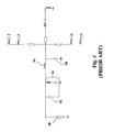
- Figure 4 is an electrical representation of a conventional output matching structure as it is used in an RF simulator.
- the extreme left element 50 is a port, and represents the current source of the device (this is the reference plane for the impedance simulations from Figure 5A and 5B )
- the shunt capacitance 52 on its right represents Cds, the shunt capacitance drain to source from the FET.
- the next three elements are matching elements inside the package (the series LC network 54 to ground, and the series inductance 56).
- the next shunt capacitance 58 represents the package lead.
- the output matching network On the right side of the lead, is represented the output matching network, to 50 ohms, on the PCB, and the connection to the power supply, through a quarter wave element, and RF and baseband decoupling shunt capacitors.
- Figure 4 represents an electrical circuit, as used in a simulator, describing the typical passive elements from the current source of an active device to 50 ohms, through internal and external (to the package) matching elements, as well as connection to the DC power supply.
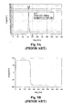
- Figure 5A is a graph illustrating a variation of the magnitude of baseband impedance with operating frequency for the RF amplifier circuit of Figure 4 .
- Figure 5B is a graph illustrating a variation of the phase of baseband impedance with operating frequency for the conventional RF amplifier circuit of Figure 4 .
- Figures 5A and 5B thus illustrate the frequency response of the conventional RF amplifier circuit of Figure 4 . From Figures 5A and 5B it will be seen that the resonant frequency of the conventional RF amplifier circuit of Figure 4 is 161MHz. This does not meet desired video bandwidth requirements for modern applications like mobile telecommunications.
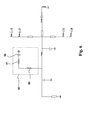
- FIG. 6 is a schematic circuit diagram of an RF amplifier circuit according to another embodiment. It will be seen that the circuit of Figure 6 differs from the conventional circuit of Figure 4 in that the shunt inductance arrangement has been removed to leave a low pass capacitor arrangement. Also, the circuit comprises an additional baseband decoupling network (identified by a dashed line labelled 85) in parallel with the RF matching network.
- the baseband decoupling network 85 is provided in addition to any envelope decoupling network that may be present external to a package of the circuit.
- This extra baseband decoupling network 85 comprises a decoupling capacitor 86 and two further inductances 87 and 88 connected in series between the drain side RF decoupling capacitance 16d and ground.
- the output of the amplifying device is then connected, via a wire bond 90, to a low pass matching network of the metallised portion of the alumina conducting ring.
- This arrangement provides a short connecting inductance to the amplifier circuit.
- Figure 8A is a graph illustrating a variation of the magnitude of baseband impedance with operating frequency for the RF amplifier circuit of Figures 6 and 7 .
- Figure 8B is a graph illustrating a variation of the phase of baseband impedance with operating frequency for the RF amplifier circuit of Figures 6 and7.
- Figures 8A and 8B thus illustrate the frequency response of the RF amplifier circuit according to the embodiment of Figures 6 and 7 . From Figures 8A and 8B it will be seen that the resonant frequency of the embodiment of Figures 6 and 7 is significantly increased when compared to the conventional circuit of Figure 4 .
- Embodiments employing the described concept of using a low pass matching network at the output of the amplifying device, in conjunction with an additional decoupling network, therefore have a higher resonant frequency which meets desired video bandwidth requirements for modern applications like mobile telecommunications.
- the embodiment shown in Figures 6 and 7 may be modified as shown in Figure 9 .
- the low pass matching network of the metallised portion of the alumina conducting ring is connected to the RF decoupling capacitance 16d on the drain side of the amplifier circuit using a plurality of parallel wire bonds 95.
- This arrangement provides a short connecting inductance.
- the plurality of bond wires 95 used for the connection realises a small inductance.
- Embodiments employ a concept of improving video bandwidth on the output side with a low pass pre-matching network.
- a low pass matching network may be used, inside a packaged RF amplifier circuit, at the output of the amplifying device in parallel with RF matching network, connected in parallel to the drain of the transistor or the shunt capacitance of the package.
- Such connection of a capacitance to the transistor drain or shunt capacitance of the RF matching network may be made using an inductive connection of large enough value to be a choke but not too large to reduce video bandwidth performance.
- Embodiments thus provide RF amplifier circuit arrangements having improved video bandwidth and/or signal distortion performance.
- a computer program may be stored/distributed on a suitable medium, such as an optical storage medium or a solid-state medium supplied together with or as part of other hardware, but may also be distributed in other forms, such as via the Internet or other wired or wireless telecommunication systems. Any reference signs in the claims should not be construed as limiting the scope.
Landscapes
- Engineering & Computer Science (AREA)
- Power Engineering (AREA)
- Microelectronics & Electronic Packaging (AREA)
- Amplifiers (AREA)
Abstract
Description
- This invention relates to the field of amplifier circuits, and more particularly to radio frequency power amplifier circuits.
- Power amplifier circuits are widely used in Radio Frequency (RF) applications. The video bandwidth, or instantaneous bandwidth, of a RF power amplifier represents the ability of the RF power amplifier to instantaneously amplify a linear signal (i.e. a signal with a variable envelope) without asymmetrical distortion.
- Thus, the instantaneous bandwidth represents the broadest modulating signal that can be handled instantaneously by a RF power amplifier without asymmetrical distortion.
- Asymmetry in signal distortion is generally unacceptable because it is difficult to correct.
- For mobile communication applications, signal modulations have become increasingly wideband over the past years (from 200kHz to 75MHz today and >100MHz in the future) so as to achieve higher data rates. Video bandwidth is therefore of growing importance and typically a discriminating factor in the field of amplification for mobile communication applications.
-
Figure 1 is a schematic diagram of a conventional discrete (i.e. packaged) RF-LDMOS power amplifier 10. The amplifying transistors are located onsilicon dies 12 provided within the package. Thepackage 10 further includes a matching network consisting ofbond wires 14 and discrete capacitors 16.Gate input leads 18 are connected to the transistor gates via gate-side capacitors 16g and drain output leads 20 are connected to the transistor drains via drain-side capacitors 16d. - Turning to
Figure 2 , there is illustrated a set of bond-wire connections between capacitors and a die of the device ofFigure 1 . The bond-wire connection between the gate-side capacitor 16g (Cpr) and the gate terminal G of the package has an inductance denoted Lg2, and the bond-wire connection between the gate-side capacitor 16g (Cpr) and the gate of the transistor on the die (DIE) has an inductance denoted Lg1. Similarly, the bond-wire connection between the drain of the transistor on the die (DIE) and the drain terminal D of the package has an inductance denoted Ld, and the bond-wire connection between the drain-side capacitor 16d (Cpo) and the drain of the transistor on the die (DIE) has an inductance denoted Li. An equivalent circuit diagram of the device ofFigure 1 illustrating the relative connections of the capacitances and inductances is provided inFigure 3 . From this, it will be seen that a capacitance Cpkg is present at each of the gate and drain terminals of the package (connected in parallel with the other capacitances), and that a source inductance Ls is associated with the source terminal of thepackage 10. - The conventional implementation described above leads to insufficient results in terms of video bandwidth (VBW) performance, signal distortion, and linearity degradation, and ultimately may not meet the minimum requirements imposed by modern telecommunications standards.
- Proposed are concepts for improving VBW performance of a RF amplifier circuit.
- According to an aspect of the invention there is provided a radio frequency amplifier circuit according to an independent claim.
- Embodiments may employ a baseband decoupling network that is connected in parallel with an RF matching network of the amplifier circuit. Further, a low pass matching network may be employed at the output of the amplifying device, therefore providing a higher resonant frequency which meets desired video bandwidth requirements for modern applications like mobile telecommunications.
- Embodiments thus relate to improving video bandwidth performance on the output side of an amplifier circuit.
- Examples of the invention will now be described in detail with reference to the accompanying drawings, in which:
-
Figure 1 is a schematic diagram of a conventional discrete (i.e. packaged) RF amplifier circuit; -
Figure 2 illustrates a set of bond-wire connections between capacitors and a die of the device ofFigure 1 ; -
Figure 3 is an equivalent circuit diagram of the device ofFigure 1 illustrating the relative connections of the capacitances and inductances; -
Figure 4 is an electrical representation of a conventional output matching structure as it is used in an RF simulator. -
Figure 5A is a graph illustrating a variation of the magnitude of baseband impedance with operating frequency for the RF amplifier circuit ofFigure 4 ; -
Figure 5B is a graph illustrating a variation of the phase of baseband impedance with operating frequency for the conventional RF amplifier circuit ofFigure 4 ; -
Figure 6 is a schematic circuit diagram of a packaged RF amplifier circuit according to an embodiment of the invention; -
Figure 7 is a plan view of the packaged RF amplifier circuit ofFigure 6 , wherein the cover of the package has been removed; -
Figure 8A is a graph illustrating a variation of the magnitude of baseband impedance with operating frequency for the RF amplifier circuit ofFigures 6 and7 ; -
Figure 8B is a graph illustrating a variation of the phase of baseband impedance with operating frequency for the RF amplifier circuit ofFigures 6 and7;and -
Figure 9 is a plan view of a packaged RF amplifier circuit according to another embodiment of the invention, wherein the cover of the package has been removed. -
Figure 4 is an electrical representation of a conventional output matching structure as it is used in an RF simulator. - From left to right, the extreme
left element 50 is a port, and represents the current source of the device (this is the reference plane for the impedance simulations fromFigure 5A and 5B ) Theshunt capacitance 52 on its right, represents Cds, the shunt capacitance drain to source from the FET. Then the next three elements are matching elements inside the package (theseries LC network 54 to ground, and the series inductance 56). Thenext shunt capacitance 58, represents the package lead. - On the right side of the lead, is represented the output matching network, to 50 ohms, on the PCB, and the connection to the power supply, through a quarter wave element, and RF and baseband decoupling shunt capacitors.
- Thus, in other words,
Figure 4 represents an electrical circuit, as used in a simulator, describing the typical passive elements from the current source of an active device to 50 ohms, through internal and external (to the package) matching elements, as well as connection to the DC power supply. -
Figure 5A is a graph illustrating a variation of the magnitude of baseband impedance with operating frequency for the RF amplifier circuit ofFigure 4 .Figure 5B is a graph illustrating a variation of the phase of baseband impedance with operating frequency for the conventional RF amplifier circuit ofFigure 4 .Figures 5A and 5B thus illustrate the frequency response of the conventional RF amplifier circuit ofFigure 4 . FromFigures 5A and 5B it will be seen that the resonant frequency of the conventional RF amplifier circuit ofFigure 4 is 161MHz. This does not meet desired video bandwidth requirements for modern applications like mobile telecommunications. -
Figure 6 is a schematic circuit diagram of an RF amplifier circuit according to another embodiment. It will be seen that the circuit ofFigure 6 differs from the conventional circuit ofFigure 4 in that the shunt inductance arrangement has been removed to leave a low pass capacitor arrangement. Also, the circuit comprises an additional baseband decoupling network (identified by a dashed line labelled 85) in parallel with the RF matching network. Thebaseband decoupling network 85 is provided in addition to any envelope decoupling network that may be present external to a package of the circuit. This extrabaseband decoupling network 85 comprises a decoupling capacitor 86 and twofurther inductances RF decoupling capacitance 16d and ground. - As shown in
Figure 7 , the output of the amplifying device is then connected, via awire bond 90, to a low pass matching network of the metallised portion of the alumina conducting ring. This arrangement provides a short connecting inductance to the amplifier circuit. -
Figure 8A is a graph illustrating a variation of the magnitude of baseband impedance with operating frequency for the RF amplifier circuit ofFigures 6 and7 .Figure 8B is a graph illustrating a variation of the phase of baseband impedance with operating frequency for the RF amplifier circuit ofFigures 6 and7.Figures 8A and 8B thus illustrate the frequency response of the RF amplifier circuit according to the embodiment ofFigures 6 and7 . FromFigures 8A and 8B it will be seen that the resonant frequency of the embodiment ofFigures 6 and7 is significantly increased when compared to the conventional circuit ofFigure 4 . Embodiments employing the described concept of using a low pass matching network at the output of the amplifying device, in conjunction with an additional decoupling network, therefore have a higher resonant frequency which meets desired video bandwidth requirements for modern applications like mobile telecommunications. - The embodiment shown in
Figures 6 and7 may be modified as shown inFigure 9 . Here, the low pass matching network of the metallised portion of the alumina conducting ring is connected to theRF decoupling capacitance 16d on the drain side of the amplifier circuit using a plurality ofparallel wire bonds 95. This arrangement provides a short connecting inductance. Specifically, the plurality ofbond wires 95 used for the connection realises a small inductance. - Embodiments employ a concept of improving video bandwidth on the output side with a low pass pre-matching network. A low pass matching network may be used, inside a packaged RF amplifier circuit, at the output of the amplifying device in parallel with RF matching network, connected in parallel to the drain of the transistor or the shunt capacitance of the package. Such connection of a capacitance to the transistor drain or shunt capacitance of the RF matching network may be made using an inductive connection of large enough value to be a choke but not too large to reduce video bandwidth performance.
- Embodiments thus provide RF amplifier circuit arrangements having improved video bandwidth and/or signal distortion performance.
- Other variations to the disclosed embodiments can be understood and effected by those skilled in the art in practicing the claimed invention, from a study of the drawings, the disclosure, and the appended claims. In the claims, the word "comprising" does not exclude other elements or steps, and the indefinite article "a" or "an" does not exclude a plurality. A single processor or other unit may fulfil the functions of several items recited in the claims. The mere fact that certain measures are recited in mutually different dependent claims does not indicate that a combination of these measured cannot be used to advantage. A computer program may be stored/distributed on a suitable medium, such as an optical storage medium or a solid-state medium supplied together with or as part of other hardware, but may also be distributed in other forms, such as via the Internet or other wired or wireless telecommunication systems. Any reference signs in the claims should not be construed as limiting the scope.
Claims (10)
- A radio frequency, RF, amplifier circuit comprising an amplifier circuit having a low-pass RF matching network comprising a RF matching capacitance, wherein the amplifier circuit further comprises a baseband decoupling network connected in parallel with the low-pass RF matching network.
- The circuit of claim 1, wherein the baseband decoupling network comprises a decoupling capacitor and an inductance connected in series between the RF matching capacitance and ground.
- The circuit of claim 1, wherein the baseband decoupling network comprises a decoupling capacitor and an inductance connected in series between the transistor drain and ground.
- The circuit of claim 1, 2 or 3, wherein the output of the amplifier circuit is connected to a low pass matching network via an inductive connection.
- The circuit of claim 4, wherein the inductive connection comprises at least one wire bond.
- The circuit of claims 1 or 2, wherein the RF matching capacitance is connected to a low pass matching network via an inductive connection.
- The circuit of claim 6, wherein the inductive connection comprises at least one wire bond.
- A packaged RF amplifier circuit comprising a RF amplifier circuit according to any preceding claim, wherein the baseband decoupling network is provided inside the packaging.
- An integrated circuit comprising an amplifier circuit according to any of claims 1 to 8.
- A mobile base station comprising an amplifier circuit according to any of claims 1 to 8.
Priority Applications (2)
| Application Number | Priority Date | Filing Date | Title |
|---|---|---|---|
| EP12290347.9A EP2722981A1 (en) | 2012-10-16 | 2012-10-16 | Amplifier circuits |
| US14/054,681 US9257946B2 (en) | 2012-10-16 | 2013-10-15 | Amplifier circuits |
Applications Claiming Priority (1)
| Application Number | Priority Date | Filing Date | Title |
|---|---|---|---|
| EP12290347.9A EP2722981A1 (en) | 2012-10-16 | 2012-10-16 | Amplifier circuits |
Publications (1)
| Publication Number | Publication Date |
|---|---|
| EP2722981A1 true EP2722981A1 (en) | 2014-04-23 |
Family
ID=47257719
Family Applications (1)
| Application Number | Title | Priority Date | Filing Date |
|---|---|---|---|
| EP12290347.9A Withdrawn EP2722981A1 (en) | 2012-10-16 | 2012-10-16 | Amplifier circuits |
Country Status (2)
| Country | Link |
|---|---|
| US (1) | US9257946B2 (en) |
| EP (1) | EP2722981A1 (en) |
Families Citing this family (1)
| Publication number | Priority date | Publication date | Assignee | Title |
|---|---|---|---|---|
| EP2722880B1 (en) | 2012-10-16 | 2018-02-28 | Ampleon Netherlands B.V. | Packaged RF amplifier circuit |
Citations (5)
| Publication number | Priority date | Publication date | Assignee | Title |
|---|---|---|---|---|
| EP0475116A2 (en) * | 1990-08-31 | 1992-03-18 | Texas Instruments Incorporated | Monolithically realizable radio frequency bias choke |
| US6229408B1 (en) * | 1999-05-19 | 2001-05-08 | Intermec Ip Corp. | Zero loss bias “T” |
| EP1347572A1 (en) * | 2000-12-28 | 2003-09-24 | Matsushita Electric Industrial Co., Ltd. | High-frequency amplifier |
| US20040041634A1 (en) * | 2002-08-30 | 2004-03-04 | Kabushiki Kaisha Toshiba | High-frequency power amplifier |
| US20040178854A1 (en) * | 2003-03-14 | 2004-09-16 | Mitsubishi Denki Kabushiki Kaisha | Semiconductor device having balanced circuit for use in high frequency band |
Family Cites Families (5)
| Publication number | Priority date | Publication date | Assignee | Title |
|---|---|---|---|---|
| FR2524712B1 (en) | 1982-03-31 | 1985-06-07 | Radiotechnique Compelec | MICROWAVE CIRCUIT WITH INTEGRATED CAPACITOR AND APPLICATION TO A SUPPLY CIRCUIT |
| US6072211A (en) | 1998-08-03 | 2000-06-06 | Motorola, Inc. | Semiconductor package |
| US9041470B2 (en) * | 2008-04-22 | 2015-05-26 | Freescale Semiconductor, Inc. | Wireless communication unit and semiconductor device having a power amplifier therefor |
| US7986184B2 (en) * | 2009-12-18 | 2011-07-26 | Nxp B.V. | Radio frequency amplifier with effective decoupling |
| EP2722880B1 (en) | 2012-10-16 | 2018-02-28 | Ampleon Netherlands B.V. | Packaged RF amplifier circuit |
-
2012
- 2012-10-16 EP EP12290347.9A patent/EP2722981A1/en not_active Withdrawn
-
2013
- 2013-10-15 US US14/054,681 patent/US9257946B2/en not_active Expired - Fee Related
Patent Citations (5)
| Publication number | Priority date | Publication date | Assignee | Title |
|---|---|---|---|---|
| EP0475116A2 (en) * | 1990-08-31 | 1992-03-18 | Texas Instruments Incorporated | Monolithically realizable radio frequency bias choke |
| US6229408B1 (en) * | 1999-05-19 | 2001-05-08 | Intermec Ip Corp. | Zero loss bias “T” |
| EP1347572A1 (en) * | 2000-12-28 | 2003-09-24 | Matsushita Electric Industrial Co., Ltd. | High-frequency amplifier |
| US20040041634A1 (en) * | 2002-08-30 | 2004-03-04 | Kabushiki Kaisha Toshiba | High-frequency power amplifier |
| US20040178854A1 (en) * | 2003-03-14 | 2004-09-16 | Mitsubishi Denki Kabushiki Kaisha | Semiconductor device having balanced circuit for use in high frequency band |
Also Published As
| Publication number | Publication date |
|---|---|
| US20140104004A1 (en) | 2014-04-17 |
| US9257946B2 (en) | 2016-02-09 |
Similar Documents
| Publication | Publication Date | Title |
|---|---|---|
| KR102249569B1 (en) | Semiconductor device | |
| US9685915B2 (en) | Amplification stage and wideband power amplifier | |
| EP2879174B1 (en) | Packaged RF power transistor device having next to each other ground leads and a video lead for connecting decoupling capacitors, RF power amplifier | |
| US9270233B2 (en) | Amplifier circuits | |
| US10453810B2 (en) | Integrated passive device for RF power amplifier package | |
| EP3340462A1 (en) | Multi baseband termination components for rf power amplifier with enhanced video bandwidth | |
| KR20200091867A (en) | RF power amplifier with combined baseband, fundamental and harmonic tuning network | |
| US8299857B2 (en) | RF power amplifier including broadband input matching network | |
| US20200059204A1 (en) | Amplifiers with broadband impedance matching and methods of manufacture thereof | |
| US20140333385A1 (en) | Dual-band semiconductor rf amplifier device | |
| CN104378074A (en) | Combiner circuit for a class-E outphasing power amplifier | |
| US9800208B2 (en) | Radio frequency devices with surface-mountable capacitors for decoupling and methods thereof | |
| US9257946B2 (en) | Amplifier circuits | |
| CN107547054B (en) | Separated compensation inductance internal matching power amplifier | |
| CN117595810A (en) | doherty amplifier | |
| EP2722982A1 (en) | Amplifier circuits | |
| US9070565B2 (en) | Power RF amplifiers | |
| KR101563212B1 (en) | Semiconductor package for high power transistor | |
| EP3142252B1 (en) | Video bandwidth in rf amplifiers | |
| CN110752195A (en) | Radio frequency power chip packaging structure |
Legal Events
| Date | Code | Title | Description |
|---|---|---|---|
| PUAI | Public reference made under article 153(3) epc to a published international application that has entered the european phase |
Free format text: ORIGINAL CODE: 0009012 |
|
| AK | Designated contracting states |
Kind code of ref document: A1 Designated state(s): AL AT BE BG CH CY CZ DE DK EE ES FI FR GB GR HR HU IE IS IT LI LT LU LV MC MK MT NL NO PL PT RO RS SE SI SK SM TR |
|
| AX | Request for extension of the european patent |
Extension state: BA ME |
|
| 17P | Request for examination filed |
Effective date: 20140326 |
|
| RBV | Designated contracting states (corrected) |
Designated state(s): AL AT BE BG CH CY CZ DE DK EE ES FI FR GB GR HR HU IE IS IT LI LT LU LV MC MK MT NL NO PL PT RO RS SE SI SK SM TR |
|
| RAP1 | Party data changed (applicant data changed or rights of an application transferred) |
Owner name: SAMBA HOLDCO NETHERLANDS B.V. |
|
| RAP1 | Party data changed (applicant data changed or rights of an application transferred) |
Owner name: AMPLEON NETHERLANDS B.V. |
|
| 17Q | First examination report despatched |
Effective date: 20160628 |
|
| STAA | Information on the status of an ep patent application or granted ep patent |
Free format text: STATUS: THE APPLICATION IS DEEMED TO BE WITHDRAWN |
|
| 18D | Application deemed to be withdrawn |
Effective date: 20170301 |