EP2722902A1 - Self-referenced MRAM element and device having improved magnetic field - Google Patents
Self-referenced MRAM element and device having improved magnetic field Download PDFInfo
- Publication number
- EP2722902A1 EP2722902A1 EP12290360.2A EP12290360A EP2722902A1 EP 2722902 A1 EP2722902 A1 EP 2722902A1 EP 12290360 A EP12290360 A EP 12290360A EP 2722902 A1 EP2722902 A1 EP 2722902A1
- Authority
- EP
- European Patent Office
- Prior art keywords
- branch
- magnetic tunnel
- mram
- field
- tunnel junction
- Prior art date
- Legal status (The legal status is an assumption and is not a legal conclusion. Google has not performed a legal analysis and makes no representation as to the accuracy of the status listed.)
- Granted
Links
Images

Classifications
-
- H—ELECTRICITY
- H10—SEMICONDUCTOR DEVICES; ELECTRIC SOLID-STATE DEVICES NOT OTHERWISE PROVIDED FOR
- H10B—ELECTRONIC MEMORY DEVICES
- H10B61/00—Magnetic memory devices, e.g. magnetoresistive RAM [MRAM] devices
-
- G—PHYSICS
- G11—INFORMATION STORAGE
- G11C—STATIC STORES
- G11C11/00—Digital stores characterised by the use of particular electric or magnetic storage elements; Storage elements therefor
- G11C11/02—Digital stores characterised by the use of particular electric or magnetic storage elements; Storage elements therefor using magnetic elements
- G11C11/14—Digital stores characterised by the use of particular electric or magnetic storage elements; Storage elements therefor using magnetic elements using thin-film elements
- G11C11/15—Digital stores characterised by the use of particular electric or magnetic storage elements; Storage elements therefor using magnetic elements using thin-film elements using multiple magnetic layers
-
- G—PHYSICS
- G11—INFORMATION STORAGE
- G11C—STATIC STORES
- G11C11/00—Digital stores characterised by the use of particular electric or magnetic storage elements; Storage elements therefor
- G11C11/02—Digital stores characterised by the use of particular electric or magnetic storage elements; Storage elements therefor using magnetic elements
- G11C11/16—Digital stores characterised by the use of particular electric or magnetic storage elements; Storage elements therefor using magnetic elements using elements in which the storage effect is based on magnetic spin effect
-
- G—PHYSICS
- G11—INFORMATION STORAGE
- G11C—STATIC STORES
- G11C11/00—Digital stores characterised by the use of particular electric or magnetic storage elements; Storage elements therefor
- G11C11/02—Digital stores characterised by the use of particular electric or magnetic storage elements; Storage elements therefor using magnetic elements
- G11C11/16—Digital stores characterised by the use of particular electric or magnetic storage elements; Storage elements therefor using magnetic elements using elements in which the storage effect is based on magnetic spin effect
- G11C11/161—Digital stores characterised by the use of particular electric or magnetic storage elements; Storage elements therefor using magnetic elements using elements in which the storage effect is based on magnetic spin effect details concerning the memory cell structure, e.g. the layers of the ferromagnetic memory cell
-
- G—PHYSICS
- G11—INFORMATION STORAGE
- G11C—STATIC STORES
- G11C11/00—Digital stores characterised by the use of particular electric or magnetic storage elements; Storage elements therefor
- G11C11/02—Digital stores characterised by the use of particular electric or magnetic storage elements; Storage elements therefor using magnetic elements
- G11C11/16—Digital stores characterised by the use of particular electric or magnetic storage elements; Storage elements therefor using magnetic elements using elements in which the storage effect is based on magnetic spin effect
- G11C11/165—Auxiliary circuits
- G11C11/1659—Cell access
-
- G—PHYSICS
- G11—INFORMATION STORAGE
- G11C—STATIC STORES
- G11C11/00—Digital stores characterised by the use of particular electric or magnetic storage elements; Storage elements therefor
- G11C11/02—Digital stores characterised by the use of particular electric or magnetic storage elements; Storage elements therefor using magnetic elements
- G11C11/16—Digital stores characterised by the use of particular electric or magnetic storage elements; Storage elements therefor using magnetic elements using elements in which the storage effect is based on magnetic spin effect
- G11C11/165—Auxiliary circuits
- G11C11/1673—Reading or sensing circuits or methods
-
- G—PHYSICS
- G11—INFORMATION STORAGE
- G11C—STATIC STORES
- G11C11/00—Digital stores characterised by the use of particular electric or magnetic storage elements; Storage elements therefor
- G11C11/02—Digital stores characterised by the use of particular electric or magnetic storage elements; Storage elements therefor using magnetic elements
- G11C11/16—Digital stores characterised by the use of particular electric or magnetic storage elements; Storage elements therefor using magnetic elements using elements in which the storage effect is based on magnetic spin effect
- G11C11/165—Auxiliary circuits
- G11C11/1675—Writing or programming circuits or methods
-
- H—ELECTRICITY
- H10—SEMICONDUCTOR DEVICES; ELECTRIC SOLID-STATE DEVICES NOT OTHERWISE PROVIDED FOR
- H10B—ELECTRONIC MEMORY DEVICES
- H10B61/00—Magnetic memory devices, e.g. magnetoresistive RAM [MRAM] devices
- H10B61/20—Magnetic memory devices, e.g. magnetoresistive RAM [MRAM] devices comprising components having three or more electrodes, e.g. transistors
-
- H—ELECTRICITY
- H10—SEMICONDUCTOR DEVICES; ELECTRIC SOLID-STATE DEVICES NOT OTHERWISE PROVIDED FOR
- H10N—ELECTRIC SOLID-STATE DEVICES NOT OTHERWISE PROVIDED FOR
- H10N50/00—Galvanomagnetic devices
- H10N50/10—Magnetoresistive devices
-
- H—ELECTRICITY
- H10—SEMICONDUCTOR DEVICES; ELECTRIC SOLID-STATE DEVICES NOT OTHERWISE PROVIDED FOR
- H10N—ELECTRIC SOLID-STATE DEVICES NOT OTHERWISE PROVIDED FOR
- H10N50/00—Galvanomagnetic devices
- H10N50/80—Constructional details
-
- H—ELECTRICITY
- H10—SEMICONDUCTOR DEVICES; ELECTRIC SOLID-STATE DEVICES NOT OTHERWISE PROVIDED FOR
- H10N—ELECTRIC SOLID-STATE DEVICES NOT OTHERWISE PROVIDED FOR
- H10N50/00—Galvanomagnetic devices
- H10N50/80—Constructional details
- H10N50/85—Materials of the active region
-
- H—ELECTRICITY
- H10—SEMICONDUCTOR DEVICES; ELECTRIC SOLID-STATE DEVICES NOT OTHERWISE PROVIDED FOR
- H10B—ELECTRONIC MEMORY DEVICES
- H10B61/00—Magnetic memory devices, e.g. magnetoresistive RAM [MRAM] devices
- H10B61/20—Magnetic memory devices, e.g. magnetoresistive RAM [MRAM] devices comprising components having three or more electrodes, e.g. transistors
- H10B61/22—Magnetic memory devices, e.g. magnetoresistive RAM [MRAM] devices comprising components having three or more electrodes, e.g. transistors of the field-effect transistor [FET] type
Definitions
- the present disclosure concerns a self-referenced magnetic random access memory (MRAM) element having a field line adapted to provide an improved magnetic field.
- MRAM magnetic random access memory
- the present disclosure further concerns a self-referenced MRAM device comprising the MRAM elements.
- Self-referenced MRAM devices comprise a plurality of MRAM cells sharing common conducting lines.
- the plurality of MRAM cells can share a field line being arranged for passing a field current for generating a magnetic field destined to the writing of the MRAM cells and/or to the reading of the MRAM cells.
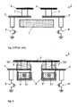
- Fig. 1 illustrates a self-referenced MRAM element such as the one described in patent US8031519 by the present applicant. More particularly, the elevation view of Fig. 1 shows the MRAM element 1 comprising a first and second magnetic tunnel junction 2, 2', a first strap 7 electrically connecting one end of the first magnetic tunnel junction 2 to a first CMOS selection transistor 8, and a second strap 7' electrically connecting one end of the second magnetic tunnel junction 2' to a second CMOS selection transistor 8'.
- the MRAM element further comprises a common field line 5 addressing the first and second magnetic tunnel junction 2, 2', and a current line 3 connected to the other end of the first and second magnetic tunnel junction 2, 2'.
- Fig. 1 illustrates a self-referenced MRAM element such as the one described in patent US8031519 by the present applicant. More particularly, the elevation view of Fig. 1 shows the MRAM element 1 comprising a first and second magnetic tunnel junction 2, 2', a first strap 7 electrically connecting one end of the first magnetic tunnel
- Fig. 2 is a top view of a self-referenced MRAM device comprising a plurality of the MRAM elements 1. In the figure, the MRAM elements 1 are arranged in a row, along the field line 5.
- Fig. 3 represents another possible configuration of a MRAM element 1 where each magnetic tunnel junction 2 is connected to a current line 3 being arranged parallel to the field line 5.
- a magnetic field generated by the field current passing in the field line 5 varies a magnetoresistance of the magnetic tunnel junction 2, such that the MRAM element 1 can be written or read.
- Writing and/or reading the MRAM element requires passing the field current with a magnitude being high enough for the generated magnetic field to be able to vary / switch a magnetization of the magnetic tunnel junction 2.
- the magnetic field should have a magnitude being typically comprised between 0 and 200 Oe, and preferably between 50 and 100 Oe.
- the present disclosure concerns a self-reference-based MRAM element comprising a first magnetic tunnel junctions and a second magnetic tunnel junctions, each having a magnetoresistance that can be varied; and a field line for passing a field current destined to vary the magnetoresistance of the first and second magnetic tunnel junctions; the field line comprising a first branch and a second branch electrically connected in parallel with the first branch, the first branch being arranged for passing a first portion of the field current to selectively vary the magnetoresistance of the first magnetic tunnel junction, and the second branch being arranged for passing a second portion of the field current to selectively vary the magnetoresistance of the second magnetic tunnel junction.
- the first and second branches can be arranged so that a first portion of magnetic field generated by passing the first portion of field current in the first branch can only vary the magnetization of the first magnetic tunnel junction, and a second portion of magnetic field generated by passing the second portion of field current in the second branch can only vary the magnetization of the second magnetic tunnel junction.
- each of the first and second branches can comprise a cladding.
- Each of the first and second branches can have a rectangular cross section, and the cladding can be comprised on three sides of the rectangular cross section.
- the cladding can comprise a ferromagnetic material such as a NiFeCo alloy.
- the MRAM element can further comprise at least one current line electrically connected to one end each of the first and second magnetic tunnel junctions.
- the present disclosure also concerns a MRAM device comprising a plurality of the MRAM elements.
- the plurality of the MRAM elements can be arranged in rows and columns, and the field line can extend along a row of MRAM elements with the first branch extending along the first magnetic tunnel junctions such as to selectively vary the magnetoresistance of the first magnetic tunnel junction of the MRAM elements in the row when the first portion of the field current is passed.
- the second branch can extend along the second magnetic tunnel junctions such as to selectively vary the magnetoresistance of the second magnetic tunnel junction of the MRAM elements in the row when the second portion of the field current is passed.
- the disclosed self-referenced MRAM element and MRAM device can use a reduced field current in comparison to the one used in conventional self-referenced MRAM elements and devices.
- the magnetoresistance of the first and second magnetic tunnel junctions can also be varied with increased selectivity.
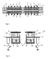
- Fig. 4 illustrates an elevation view of a self-reference MRAM element 1 according to an embodiment.
- the MRAM element 1 comprises a first magnetic tunnel junction 2 and a second magnetic tunnel junction 2', a field line 5 for passing a field current 51.
- the first and second magnetic tunnel junction 2, 2' comprises a magnetoresistance that can be varied with an external magnetic field.
- the first and second magnetic tunnel junction 2, 2' comprises a first ferromagnetic layer having a first magnetization that can be varied with the magnetic field, a barrier layer, and a second ferromagnetic layer having a second magnetization that is fixed or that can also be varied in the magnetic field.
- the magnetic field varying the magnetoresistance of the first and second magnetic tunnel junctions 2, 2' is generated by passing the field current 51 in the field line 5.
- the field line 5 comprises a first branch 5' and a second branch 5" electrically connected in parallel with the first branch 5'.
- the first branch 5' is arranged for passing a first portion 51' of the field current and the second branch 5" is arranged for passing a second portion 51" of the field current.
- the first portion 51' of the field current generates a first portion 52' of magnetic field that is capable of switching the first magnetization of the first ferromagnetic layer (or the second magnetization of the second ferromagnetic layer), such as to vary the magnetoresistance of the first magnetic tunnel junction 2.
- the second portion 51" of the field current generates a second portion 52" of magnetic field that is capable of varying the magnetoresistance of the second magnetic tunnel junction 2'.
- the first and second branches 5', 5" are arranged so that the first portion 52' of magnetic field generated by passing the first portion 51' of field current in the first branch 5' can only vary the magnetization of the first magnetic tunnel junction 2, and the second portion 52" of magnetic field generated by passing the second portion 51 " of field current in the second branch 5" can only vary the magnetization of the second magnetic tunnel junction 2'.
- the MRAM element 1 further comprise a first strap 7 electrically connecting one end of the first magnetic tunnel junction 2 to a first CMOS selection transistor 8, and a second strap 7' electrically connecting one end of the second magnetic tunnel junction 2' to a second CMOS selection transistor 8'.
- the strap 7, 7' allows for placing the first and second branch 5', 5" underneath the first and second magnetic tunnel junction 2, 2', respectively, such that the first and second branches 5', 5" can be located in close proximity to the first and second magnetic tunnel junction 2, 2', respectively.
- the proximity of the first and second branch 5', 5" to the first and second magnetic tunnel junctions 2, 2' alloys for the generated first magnetic field 52' to interact only with the first magnetic layer 2 and the generated second magnetic field 52" to interact only with the second magnetic layer 2'. This arrangement thus allows for improving the selectivity in varying the magnetoresistance of the first and second magnetic tunnel junctions 2, 2' during writing and/or reading operation.
- the MRAM element 1 can further comprise a current line 3 connected to the other end of the first and second magnetic tunnel junction 2, 2'.
- the first and second branches 5', 5" are represented orthogonal to the page and to the current line 3.
- a heating current 31 can be passed in the current line 3 and in the magnetic tunnel junction 2, 2' having its transistor 8, 8' being set in a passing mode.
- each of the first and second branches 5', 5" comprise a cladding 6.
- the first and second branch 5', 5" has a rectangular cross section.
- the cladding 6 embeds three sides of the rectangular cross section, leaving the side proximal to the magnetic tunnel junction 2, 2' uncladded.
- the cladding 6 focuses the magnetic field 52', 52" towards the magnetic tunnel junction 2, 2', increasing the intensity of the magnetic field 52', 52" in the region of the magnetic tunnel junction 2, 2' as compared to the magnetic field produced by uncladded branches 5', 5".
- the magnetic field 52', 52" is represented by the magnetic flux lines closing tightly on each branch 5', 5" due to the proximity of the two opposite sides of the cladding 6. Consequently, the cladding 6 allows for using a reduced field current 51', 51", in comparison to the one required with uncladded branches 5', 5", to generate a magnetic field able to vary the magnetoresistance of the magnetic tunnel junction 2, 2'.
- the branches 5', 5" are represented with a rectangular cross section in Fig. 4 , it will be understood that other forms or shapes of the branches 5', 5" could be used and all such forms or shapes can incorporate the described sides, and can include a width and a depth.
- the cladding can comprise a soft ferromagnetic material.
- the soft ferromagnetic material can include ferromagnetic materials that have high magnetic permeability, such as NiFeCo alloys. With a high permeability, the cladding magnetization rotates in response to the generated magnetic field which enables the focusing and enhancement of the magnetic field 52', 52" in the portion of the branch 5', 5" comprising the cladding 6. Moreover, in the region of the first and second magnetic tunnel junctions 2, 2', the magnetic field 52', 52" has a component being substantially parallel to the plan of the ferromagnetic layer magnetization being written (or read).
- Fig. 5 is a top view showing a self-reference MRAM device comprising a plurality of the MRAM elements 1, according to an embodiment. More particularly, Fig. 5 shows the common field line 5 extending along a row of MRAM elements 1 such as to address the MRAM elements 1 along this row.
- the field line 5 comprises the first branch 5' extending along the first magnetic tunnel junctions 2 and the second branch 5" extending along the second magnetic tunnel junctions 2'.
- the two ends of the field line 5 are electrically connected such that when the field current 51 is passed in the field line, the first portion 51' of the field current passes in the first branch 5', addressing the first magnetic tunnel junctions 2, and the second portion 51" of the field current passes in the second branch 5", addressing the second magnetic tunnel junctions 2'.
- the first portion 51' of the field current can generate the first portion 52' of magnetic field adapted to selectively vary the magnetoresistance of the first magnetic tunnel junctions 2 along the row
- the second portion 51" of the field current can generate the second portion 52" of magnetic field adapted to selectively vary the magnetoresistance of the second magnetic tunnel junctions 2' along the row.
- the two substantially parallel branches 5', 5" are formed by an opening 9 provided in the common field line 5.
- Fig. 6 represents the self-reference MRAM element 1 according to another embodiment, wherein the current line 3 is arranged substantially parallel to the first and second branches 5', 5".
Landscapes
- Engineering & Computer Science (AREA)
- Computer Hardware Design (AREA)
- Hall/Mr Elements (AREA)
- Mram Or Spin Memory Techniques (AREA)
- Semiconductor Memories (AREA)
Abstract
Description
- The present disclosure concerns a self-referenced magnetic random access memory (MRAM) element having a field line adapted to provide an improved magnetic field. The present disclosure further concerns a self-referenced MRAM device comprising the MRAM elements.
- Self-referenced MRAM devices comprise a plurality of MRAM cells sharing common conducting lines. In particular, the plurality of MRAM cells can share a field line being arranged for passing a field current for generating a magnetic field destined to the writing of the MRAM cells and/or to the reading of the MRAM cells.
-
Fig. 1 illustrates a self-referenced MRAM element such as the one described in patentUS8031519 by the present applicant. More particularly, the elevation view ofFig. 1 shows theMRAM element 1 comprising a first and secondmagnetic tunnel junction 2, 2', afirst strap 7 electrically connecting one end of the firstmagnetic tunnel junction 2 to a firstCMOS selection transistor 8, and a second strap 7' electrically connecting one end of the second magnetic tunnel junction 2' to a second CMOS selection transistor 8'. The MRAM element further comprises acommon field line 5 addressing the first and secondmagnetic tunnel junction 2, 2', and acurrent line 3 connected to the other end of the first and secondmagnetic tunnel junction 2, 2'. InFig. 1 , thefield line 5 is represented orthogonal to the page and perpendicular to thecurrent line 3.Fig. 2 is a top view of a self-referenced MRAM device comprising a plurality of theMRAM elements 1. In the figure, theMRAM elements 1 are arranged in a row, along thefield line 5.Fig. 3 represents another possible configuration of aMRAM element 1 where eachmagnetic tunnel junction 2 is connected to acurrent line 3 being arranged parallel to thefield line 5. - In the above configurations of self-referenced MRAM elements, a magnetic field generated by the field current passing in the
field line 5 varies a magnetoresistance of themagnetic tunnel junction 2, such that theMRAM element 1 can be written or read. Writing and/or reading the MRAM element requires passing the field current with a magnitude being high enough for the generated magnetic field to be able to vary / switch a magnetization of themagnetic tunnel junction 2. Indeed, the magnetic field should have a magnitude being typically comprised between 0 and 200 Oe, and preferably between 50 and 100 Oe. - In low power application, such as in mobile devices, high field currents are detrimental. The same applies for applications requiring a MRAM device having a high surface density of MRAM elements where high magnetic fields must be generated by small field lines.
- Obtaining a self-referenced MRAM element and device wherein the field line is capable of generating a larger magnetic field for a given field current would thus be advantageous.
- The present disclosure concerns a self-reference-based MRAM element comprising a first magnetic tunnel junctions and a second magnetic tunnel junctions, each having a magnetoresistance that can be varied; and a field line for passing a field current destined to vary the magnetoresistance of the first and second magnetic tunnel junctions; the field line comprising a first branch and a second branch electrically connected in parallel with the first branch, the first branch being arranged for passing a first portion of the field current to selectively vary the magnetoresistance of the first magnetic tunnel junction, and the second branch being arranged for passing a second portion of the field current to selectively vary the magnetoresistance of the second magnetic tunnel junction.
- In an embodiment, the first and second branches can be arranged so that a first portion of magnetic field generated by passing the first portion of field current in the first branch can only vary the magnetization of the first magnetic tunnel junction, and a second portion of magnetic field generated by passing the second portion of field current in the second branch can only vary the magnetization of the second magnetic tunnel junction.
- In another embodiment, each of the first and second branches can comprise a cladding. Each of the first and second branches can have a rectangular cross section, and the cladding can be comprised on three sides of the rectangular cross section. The cladding can comprise a ferromagnetic material such as a NiFeCo alloy.
- In yet another embodiment, the MRAM element can further comprise at least one current line electrically connected to one end each of the first and second magnetic tunnel junctions.
- The present disclosure also concerns a MRAM device comprising a plurality of the MRAM elements. The plurality of the MRAM elements can be arranged in rows and columns, and the field line can extend along a row of MRAM elements with the first branch extending along the first magnetic tunnel junctions such as to selectively vary the magnetoresistance of the first magnetic tunnel junction of the MRAM elements in the row when the first portion of the field current is passed. The second branch can extend along the second magnetic tunnel junctions such as to selectively vary the magnetoresistance of the second magnetic tunnel junction of the MRAM elements in the row when the second portion of the field current is passed.
- The disclosed self-referenced MRAM element and MRAM device can use a reduced field current in comparison to the one used in conventional self-referenced MRAM elements and devices. The magnetoresistance of the first and second magnetic tunnel junctions can also be varied with increased selectivity.
- The disclosure will be better understood with the aid of the description of an embodiment given by way of example and illustrated by the figures, in which:
-
Fig. 1 illustrates a conventional self-referenced MRAM element; -
Fig. 2 is a top view of a self-referenced MRAM device comprising a plurality of the MRAM elements ofFig. 1 ; -
Fig. 3 represents a conventional self-referenced MRAM element in another configuration; -
Fig. 4 illustrates a self-referenced MRAM element, according to an embodiment; -
Fig. 5 is a top view showing a self-reference MRAM device comprising a plurality of the MRAM elements, according to an embodiment; and -
Fig. 6 represents the self-reference MRAM element according to another embodiment. -
Fig. 4 illustrates an elevation view of a self-reference MRAM element 1 according to an embodiment. TheMRAM element 1 comprises a firstmagnetic tunnel junction 2 and a second magnetic tunnel junction 2', afield line 5 for passing afield current 51. The first and secondmagnetic tunnel junction 2, 2' comprises a magnetoresistance that can be varied with an external magnetic field. In an embodiment not represented, the first and secondmagnetic tunnel junction 2, 2' comprises a first ferromagnetic layer having a first magnetization that can be varied with the magnetic field, a barrier layer, and a second ferromagnetic layer having a second magnetization that is fixed or that can also be varied in the magnetic field. Here, the magnetic field varying the magnetoresistance of the first and secondmagnetic tunnel junctions 2, 2' is generated by passing thefield current 51 in thefield line 5. - The
field line 5 comprises a first branch 5' and asecond branch 5" electrically connected in parallel with the first branch 5'. The first branch 5' is arranged for passing a first portion 51' of the field current and thesecond branch 5" is arranged for passing asecond portion 51" of the field current. In this arrangement, the first portion 51' of the field current generates a first portion 52' of magnetic field that is capable of switching the first magnetization of the first ferromagnetic layer (or the second magnetization of the second ferromagnetic layer), such as to vary the magnetoresistance of the firstmagnetic tunnel junction 2. Similarly, thesecond portion 51" of the field current generates asecond portion 52" of magnetic field that is capable of varying the magnetoresistance of the second magnetic tunnel junction 2'. Preferably, the first andsecond branches 5', 5" are arranged so that the first portion 52' of magnetic field generated by passing the first portion 51' of field current in the first branch 5' can only vary the magnetization of the firstmagnetic tunnel junction 2, and thesecond portion 52" of magnetic field generated by passing thesecond portion 51 " of field current in thesecond branch 5" can only vary the magnetization of the second magnetic tunnel junction 2'. - In the configuration of
Fig. 4 , theMRAM element 1 further comprise afirst strap 7 electrically connecting one end of the firstmagnetic tunnel junction 2 to a firstCMOS selection transistor 8, and a second strap 7' electrically connecting one end of the second magnetic tunnel junction 2' to a second CMOS selection transistor 8'. Thestrap 7, 7' allows for placing the first andsecond branch 5', 5" underneath the first and secondmagnetic tunnel junction 2, 2', respectively, such that the first andsecond branches 5', 5" can be located in close proximity to the first and secondmagnetic tunnel junction 2, 2', respectively. The proximity of the first andsecond branch 5', 5" to the first and secondmagnetic tunnel junctions 2, 2' alloys for the generated first magnetic field 52' to interact only with the firstmagnetic layer 2 and the generated secondmagnetic field 52" to interact only with the second magnetic layer 2'. This arrangement thus allows for improving the selectivity in varying the magnetoresistance of the first and secondmagnetic tunnel junctions 2, 2' during writing and/or reading operation. - The
MRAM element 1 can further comprise acurrent line 3 connected to the other end of the first and secondmagnetic tunnel junction 2, 2'. InFig. 1 , the first andsecond branches 5', 5" are represented orthogonal to the page and to thecurrent line 3. In the case of a thermally assisted writing operation of theMRAM element 1, a heating current 31 can be passed in thecurrent line 3 and in themagnetic tunnel junction 2, 2' having itstransistor 8, 8' being set in a passing mode. - In a preferred embodiment, at least a portion of each of the first and
second branches 5', 5" comprise acladding 6. In the particular example ofFig. 4 , the first andsecond branch 5', 5" has a rectangular cross section. Thecladding 6 embeds three sides of the rectangular cross section, leaving the side proximal to themagnetic tunnel junction 2, 2' uncladded. Thecladding 6 focuses themagnetic field 52', 52" towards themagnetic tunnel junction 2, 2', increasing the intensity of themagnetic field 52', 52" in the region of themagnetic tunnel junction 2, 2' as compared to the magnetic field produced byuncladded branches 5', 5". InFig. 4 themagnetic field 52', 52" is represented by the magnetic flux lines closing tightly on eachbranch 5', 5" due to the proximity of the two opposite sides of thecladding 6. Consequently, thecladding 6 allows for using a reducedfield current 51', 51", in comparison to the one required withuncladded branches 5', 5", to generate a magnetic field able to vary the magnetoresistance of themagnetic tunnel junction 2, 2'. - For an uncladded field line, the magnetic field H is given by the equation H = l/2 w, where l is the current flowing through the
branch 5', 5" and w is the width of thebranch 5', 5". Here, the field loss caused by the finite thickness of the branch is ignored. For thebranch 5', 5" being cladded on three sides as in the example ofFig. 4 , the magnetic field H is given by the equation H = l/w, which is a factor of two larger than the uncladded branch. While thebranches 5', 5" are represented with a rectangular cross section inFig. 4 , it will be understood that other forms or shapes of thebranches 5', 5" could be used and all such forms or shapes can incorporate the described sides, and can include a width and a depth. - In a variant of the embodiment, the cladding can comprise a soft ferromagnetic material. The soft ferromagnetic material can include ferromagnetic materials that have high magnetic permeability, such as NiFeCo alloys. With a high permeability, the cladding magnetization rotates in response to the generated magnetic field which enables the focusing and enhancement of the
magnetic field 52', 52" in the portion of thebranch 5', 5" comprising thecladding 6. Moreover, in the region of the first and secondmagnetic tunnel junctions 2, 2', themagnetic field 52', 52" has a component being substantially parallel to the plan of the ferromagnetic layer magnetization being written (or read). -
Fig. 5 is a top view showing a self-reference MRAM device comprising a plurality of theMRAM elements 1, according to an embodiment. More particularly,Fig. 5 shows thecommon field line 5 extending along a row ofMRAM elements 1 such as to address theMRAM elements 1 along this row. Thefield line 5 comprises the first branch 5' extending along the firstmagnetic tunnel junctions 2 and thesecond branch 5" extending along the second magnetic tunnel junctions 2'. The two ends of thefield line 5 are electrically connected such that when the field current 51 is passed in the field line, the first portion 51' of the field current passes in the first branch 5', addressing the firstmagnetic tunnel junctions 2, and thesecond portion 51" of the field current passes in thesecond branch 5", addressing the second magnetic tunnel junctions 2'. In this arrangement, the first portion 51' of the field current can generate the first portion 52' of magnetic field adapted to selectively vary the magnetoresistance of the firstmagnetic tunnel junctions 2 along the row, and thesecond portion 51" of the field current can generate thesecond portion 52" of magnetic field adapted to selectively vary the magnetoresistance of the second magnetic tunnel junctions 2' along the row. In the particular arrangement ofFig. 5 , the two substantiallyparallel branches 5', 5" are formed by anopening 9 provided in thecommon field line 5. -
Fig. 6 represents the self-reference MRAM element 1 according to another embodiment, wherein thecurrent line 3 is arranged substantially parallel to the first andsecond branches 5', 5". -
- 1
- magnetic random access memory (MRAM) element
- 2
- first magnetic tunnel junction
- 2'
- second magnetic tunnel junction
- 3
- current line
- 5
- field line
- 5'
- first branch
- 5"
- second branch
- 51
- field current
- 51'
- first portion of field current
- 51"
- second portion of field current
- 52'
- first magnetic field
- 52"
- second magnetic field
- 6
- cladding
- 7
- first strap
- 7'
- second strap
- 8
- first selection transistor
- 8'
- second selection transistor
- 9
- opening
- H
- magnetic field
- I
- current
- w
- width
Claims (9)
- Self-reference-based MRAM element (1) comprising
a first magnetic tunnel junction (2) and a second magnetic tunnel junction (2'), each having a magnetoresistance that can be varied; and
a field line (5) for passing a field current (51) destined to vary the magnetoresistance of the first and second magnetic tunnel junctions (2, 2');
the field line (5) comprising a first branch (5') and a second branch (5") both branch (5', 5") comprises a cladding (6);
the first branch (5') being arranged for passing a first portion (51') of the field current to selectively vary the magnetoresistance of the first magnetic tunnel junction (2),
and the second branch (5") being electrically connected in parallel with the first branch (5') and arranged for passing a second portion (51 ") of the field current to selectively vary the magnetoresistance of the second magnetic tunnel junction (2'). - MRAM element (1) according to claim 1, wherein the first and second branches (5', 5") are arranged so that a first portion (52') of magnetic field generated by passing the first portion (51') of field current in the first branch (5') can only vary the magnetization of the first magnetic tunnel junction (2), and a second portion (52") of magnetic field generated by passing the second portion (51") of field current in the second branch (5") can only vary the magnetization of the second magnetic tunnel junction (2').
- MRAM element (1) according to claim 1 or 2, wherein each of said first and second branches (5', 5") has a rectangular cross section, and wherein the cladding (6) is comprised on three sides of the rectangular cross section.
- MRAM element (1) according to any one of claims 1 to 3,
wherein
the cladding (6) comprises a ferromagnetic material. - MRAM element (1) according to claim 4, wherein
the ferromagnetic material comprises a NiFeCo alloy. - MRAM element (1) according to any one of claims 1 to 5, further comprising at least one current line (3) electrically connected to one end of each of the first and second magnetic tunnel junctions (2, 2').
- MRAM device comprising a plurality of the MRAM elements (1) characterized by any one of claims 1 to 6.
- MRAM device according to claim 7, wherein
said plurality of the MRAM elements (1) are arranged in rows and columns, and wherein the field line (5) extends along a row of MRAM elements (1) with the first branch (5') extending along the first magnetic tunnel junctions (2) such as to selectively vary the magnetoresistance of the first magnetic tunnel junction (2) of the MRAM elements (1) in the row when the first portion (51') of the field current is passed, and with the second branch (5") extending along the second magnetic tunnel junctions (2') such as to selectively vary the magnetoresistance of the second magnetic tunnel junction (2') of the MRAM elements (1) in the row when the second portion (51 ") of the field current is passed. - MRAM device according to claim 8, wherein
the first branch (5') is electrically connected with the second branch (5") at each end of the row.
Priority Applications (3)
| Application Number | Priority Date | Filing Date | Title |
|---|---|---|---|
| EP12290360.2A EP2722902B1 (en) | 2012-10-22 | 2012-10-22 | Self-referenced MRAM element and device having improved magnetic field |
| PCT/EP2013/071357 WO2014063938A1 (en) | 2012-10-22 | 2013-10-11 | Self-referenced mram element and device having improved magnetic field |
| US14/437,362 US9461093B2 (en) | 2012-10-22 | 2013-10-11 | Self-referenced MRAM element and device having improved magnetic field |
Applications Claiming Priority (1)
| Application Number | Priority Date | Filing Date | Title |
|---|---|---|---|
| EP12290360.2A EP2722902B1 (en) | 2012-10-22 | 2012-10-22 | Self-referenced MRAM element and device having improved magnetic field |
Publications (2)
| Publication Number | Publication Date |
|---|---|
| EP2722902A1 true EP2722902A1 (en) | 2014-04-23 |
| EP2722902B1 EP2722902B1 (en) | 2016-11-30 |
Family
ID=47681557
Family Applications (1)
| Application Number | Title | Priority Date | Filing Date |
|---|---|---|---|
| EP12290360.2A Active EP2722902B1 (en) | 2012-10-22 | 2012-10-22 | Self-referenced MRAM element and device having improved magnetic field |
Country Status (3)
| Country | Link |
|---|---|
| US (1) | US9461093B2 (en) |
| EP (1) | EP2722902B1 (en) |
| WO (1) | WO2014063938A1 (en) |
Families Citing this family (3)
| Publication number | Priority date | Publication date | Assignee | Title |
|---|---|---|---|---|
| EP2626861B1 (en) * | 2012-02-13 | 2015-01-07 | Crocus Technology S.A. | High speed magnetic random access memory-based ternary CAM |
| EP3115994B1 (en) * | 2015-07-07 | 2022-06-08 | Crocus Technology S.A. | Magnetic memory device that is protected against reading using an external magnetic field and method for operating such magnetic memory device |
| KR102356356B1 (en) | 2017-05-31 | 2022-01-28 | 에스케이하이닉스 주식회사 | Cleaning composition and method for fabricating electronic device using the same |
Citations (4)
| Publication number | Priority date | Publication date | Assignee | Title |
|---|---|---|---|---|
| US6597049B1 (en) * | 2002-04-25 | 2003-07-22 | Hewlett-Packard Development Company, L.P. | Conductor structure for a magnetic memory |
| US20050205952A1 (en) * | 2004-03-19 | 2005-09-22 | Jae-Hyun Park | Magnetic random access memory cells having split sub-digit lines having cladding layers thereon and methods of fabricating the same |
| US20060023490A1 (en) * | 2002-11-28 | 2006-02-02 | Koninklijke Philips Electronics N.V. | Magnetic memory architecture with shared current line |
| US8031519B2 (en) | 2008-06-18 | 2011-10-04 | Crocus Technology S.A. | Shared line magnetic random access memory cells |
Family Cites Families (3)
| Publication number | Priority date | Publication date | Assignee | Title |
|---|---|---|---|---|
| US6865105B1 (en) * | 2003-09-22 | 2005-03-08 | Hewlett-Packard Development Company, L.P. | Thermal-assisted switching array configuration for MRAM |
| KR100612878B1 (en) * | 2004-12-03 | 2006-08-14 | 삼성전자주식회사 | Magnetic memory device and its manufacture and operation method |
| EP2270812B1 (en) * | 2009-07-02 | 2017-01-18 | CROCUS Technology | Ultimate magnetic random access memory-based ternay CAM |
-
2012
- 2012-10-22 EP EP12290360.2A patent/EP2722902B1/en active Active
-
2013
- 2013-10-11 WO PCT/EP2013/071357 patent/WO2014063938A1/en not_active Ceased
- 2013-10-11 US US14/437,362 patent/US9461093B2/en active Active
Patent Citations (4)
| Publication number | Priority date | Publication date | Assignee | Title |
|---|---|---|---|---|
| US6597049B1 (en) * | 2002-04-25 | 2003-07-22 | Hewlett-Packard Development Company, L.P. | Conductor structure for a magnetic memory |
| US20060023490A1 (en) * | 2002-11-28 | 2006-02-02 | Koninklijke Philips Electronics N.V. | Magnetic memory architecture with shared current line |
| US20050205952A1 (en) * | 2004-03-19 | 2005-09-22 | Jae-Hyun Park | Magnetic random access memory cells having split sub-digit lines having cladding layers thereon and methods of fabricating the same |
| US8031519B2 (en) | 2008-06-18 | 2011-10-04 | Crocus Technology S.A. | Shared line magnetic random access memory cells |
Also Published As
| Publication number | Publication date |
|---|---|
| US20150287764A1 (en) | 2015-10-08 |
| WO2014063938A1 (en) | 2014-05-01 |
| US9461093B2 (en) | 2016-10-04 |
| EP2722902B1 (en) | 2016-11-30 |
Similar Documents
| Publication | Publication Date | Title |
|---|---|---|
| RU2599948C2 (en) | Self-referenced magnetic random access memory element comprising synthetic storage layer | |
| JP5461683B2 (en) | Magnetic memory cell and magnetic random access memory | |
| US7459769B2 (en) | Magnetic shield member, magnetic shield structure, and magnetic memory device | |
| JP2008192916A (en) | Magnetic random access memory and writing method thereof | |
| KR100552376B1 (en) | Magnetic memory | |
| EP2722902B1 (en) | Self-referenced MRAM element and device having improved magnetic field | |
| RU2591643C2 (en) | Self-referential mram cell with optimised reliability | |
| JP5092464B2 (en) | Domain wall displacement type magnetic recording element having domain wall displacement detection terminal | |
| KR100615089B1 (en) | Magnetic ram with low drive current | |
| KR100570197B1 (en) | Method of writing a magnetoresistive memory cell in an integrated magnetoresistive semiconductor memory device | |
| EP2672487A1 (en) | Method for writing to a Random Access Memory (MRAM) Cell with improved MRAM Cell Lifespan | |
| EP3115994B1 (en) | Magnetic memory device that is protected against reading using an external magnetic field and method for operating such magnetic memory device | |
| US7221583B2 (en) | Magnetic film, multilayer magnetic film, method and mechanism of magnetization inversion of magnetic film, and magnetic random access memory | |
| JP5076387B2 (en) | Magnetic storage | |
| KR100952919B1 (en) | High-capacity mram using perpendicular magnetic tunnel junction | |
| KR101474665B1 (en) | Spin Transfer Torque Magnetic Tunnel Junction device, Operation Method thereof, and Magnetoresistive Random Access Memory including them | |
| CN100463208C (en) | System for magnetic memory element including single word line transistor and method of reading and programming the same | |
| JP7056234B2 (en) | Magnetized structure, domain wall moving magnetic recording element and magnetic memory | |
| JP2007059865A (en) | Magnetic storage | |
| JP5382295B2 (en) | Magnetic random access memory | |
| JP2007165449A (en) | Magnetic storage device | |
| EP2688103A1 (en) | MRAM cell and device with improved field line for reduced power consumption | |
| JP5076373B2 (en) | Magnetic storage device and magnetic storage method | |
| JP5092384B2 (en) | Magnetic storage device and magnetic storage method | |
| JP2019079959A (en) | Domain wall displacement type magnetic recording apparatus and magnetic recording array |
Legal Events
| Date | Code | Title | Description |
|---|---|---|---|
| PUAI | Public reference made under article 153(3) epc to a published international application that has entered the european phase |
Free format text: ORIGINAL CODE: 0009012 |
|
| AK | Designated contracting states |
Kind code of ref document: A1 Designated state(s): AL AT BE BG CH CY CZ DE DK EE ES FI FR GB GR HR HU IE IS IT LI LT LU LV MC MK MT NL NO PL PT RO RS SE SI SK SM TR |
|
| AX | Request for extension of the european patent |
Extension state: BA ME |
|
| 17P | Request for examination filed |
Effective date: 20140909 |
|
| RBV | Designated contracting states (corrected) |
Designated state(s): AL AT BE BG CH CY CZ DE DK EE ES FI FR GB GR HR HU IE IS IT LI LT LU LV MC MK MT NL NO PL PT RO RS SE SI SK SM TR |
|
| 17Q | First examination report despatched |
Effective date: 20150608 |
|
| GRAP | Despatch of communication of intention to grant a patent |
Free format text: ORIGINAL CODE: EPIDOSNIGR1 |
|
| INTG | Intention to grant announced |
Effective date: 20160329 |
|
| GRAJ | Information related to disapproval of communication of intention to grant by the applicant or resumption of examination proceedings by the epo deleted |
Free format text: ORIGINAL CODE: EPIDOSDIGR1 |
|
| GRAS | Grant fee paid |
Free format text: ORIGINAL CODE: EPIDOSNIGR3 |
|
| INTC | Intention to grant announced (deleted) | ||
| GRAP | Despatch of communication of intention to grant a patent |
Free format text: ORIGINAL CODE: EPIDOSNIGR1 |
|
| INTG | Intention to grant announced |
Effective date: 20160913 |
|
| GRAA | (expected) grant |
Free format text: ORIGINAL CODE: 0009210 |
|
| AK | Designated contracting states |
Kind code of ref document: B1 Designated state(s): AL AT BE BG CH CY CZ DE DK EE ES FI FR GB GR HR HU IE IS IT LI LT LU LV MC MK MT NL NO PL PT RO RS SE SI SK SM TR |
|
| REG | Reference to a national code |
Ref country code: CH Ref legal event code: EP Ref country code: GB Ref legal event code: FG4D |
|
| REG | Reference to a national code |
Ref country code: AT Ref legal event code: REF Ref document number: 850558 Country of ref document: AT Kind code of ref document: T Effective date: 20161215 |
|
| REG | Reference to a national code |
Ref country code: IE Ref legal event code: FG4D |
|
| REG | Reference to a national code |
Ref country code: DE Ref legal event code: R096 Ref document number: 602012025974 Country of ref document: DE |
|
| PG25 | Lapsed in a contracting state [announced via postgrant information from national office to epo] |
Ref country code: LV Free format text: LAPSE BECAUSE OF FAILURE TO SUBMIT A TRANSLATION OF THE DESCRIPTION OR TO PAY THE FEE WITHIN THE PRESCRIBED TIME-LIMIT Effective date: 20161130 |
|
| REG | Reference to a national code |
Ref country code: LT Ref legal event code: MG4D |
|
| REG | Reference to a national code |
Ref country code: NL Ref legal event code: MP Effective date: 20161130 |
|
| REG | Reference to a national code |
Ref country code: AT Ref legal event code: MK05 Ref document number: 850558 Country of ref document: AT Kind code of ref document: T Effective date: 20161130 |
|
| PG25 | Lapsed in a contracting state [announced via postgrant information from national office to epo] |
Ref country code: LT Free format text: LAPSE BECAUSE OF FAILURE TO SUBMIT A TRANSLATION OF THE DESCRIPTION OR TO PAY THE FEE WITHIN THE PRESCRIBED TIME-LIMIT Effective date: 20161130 Ref country code: NO Free format text: LAPSE BECAUSE OF FAILURE TO SUBMIT A TRANSLATION OF THE DESCRIPTION OR TO PAY THE FEE WITHIN THE PRESCRIBED TIME-LIMIT Effective date: 20170228 Ref country code: SE Free format text: LAPSE BECAUSE OF FAILURE TO SUBMIT A TRANSLATION OF THE DESCRIPTION OR TO PAY THE FEE WITHIN THE PRESCRIBED TIME-LIMIT Effective date: 20161130 Ref country code: GR Free format text: LAPSE BECAUSE OF FAILURE TO SUBMIT A TRANSLATION OF THE DESCRIPTION OR TO PAY THE FEE WITHIN THE PRESCRIBED TIME-LIMIT Effective date: 20170301 |
|
| PG25 | Lapsed in a contracting state [announced via postgrant information from national office to epo] |
Ref country code: FI Free format text: LAPSE BECAUSE OF FAILURE TO SUBMIT A TRANSLATION OF THE DESCRIPTION OR TO PAY THE FEE WITHIN THE PRESCRIBED TIME-LIMIT Effective date: 20161130 Ref country code: PL Free format text: LAPSE BECAUSE OF FAILURE TO SUBMIT A TRANSLATION OF THE DESCRIPTION OR TO PAY THE FEE WITHIN THE PRESCRIBED TIME-LIMIT Effective date: 20161130 Ref country code: AT Free format text: LAPSE BECAUSE OF FAILURE TO SUBMIT A TRANSLATION OF THE DESCRIPTION OR TO PAY THE FEE WITHIN THE PRESCRIBED TIME-LIMIT Effective date: 20161130 Ref country code: HR Free format text: LAPSE BECAUSE OF FAILURE TO SUBMIT A TRANSLATION OF THE DESCRIPTION OR TO PAY THE FEE WITHIN THE PRESCRIBED TIME-LIMIT Effective date: 20161130 Ref country code: RS Free format text: LAPSE BECAUSE OF FAILURE TO SUBMIT A TRANSLATION OF THE DESCRIPTION OR TO PAY THE FEE WITHIN THE PRESCRIBED TIME-LIMIT Effective date: 20161130 Ref country code: ES Free format text: LAPSE BECAUSE OF FAILURE TO SUBMIT A TRANSLATION OF THE DESCRIPTION OR TO PAY THE FEE WITHIN THE PRESCRIBED TIME-LIMIT Effective date: 20161130 Ref country code: PT Free format text: LAPSE BECAUSE OF FAILURE TO SUBMIT A TRANSLATION OF THE DESCRIPTION OR TO PAY THE FEE WITHIN THE PRESCRIBED TIME-LIMIT Effective date: 20170330 |
|
| PG25 | Lapsed in a contracting state [announced via postgrant information from national office to epo] |
Ref country code: NL Free format text: LAPSE BECAUSE OF FAILURE TO SUBMIT A TRANSLATION OF THE DESCRIPTION OR TO PAY THE FEE WITHIN THE PRESCRIBED TIME-LIMIT Effective date: 20161130 |
|
| PG25 | Lapsed in a contracting state [announced via postgrant information from national office to epo] |
Ref country code: DK Free format text: LAPSE BECAUSE OF FAILURE TO SUBMIT A TRANSLATION OF THE DESCRIPTION OR TO PAY THE FEE WITHIN THE PRESCRIBED TIME-LIMIT Effective date: 20161130 Ref country code: CZ Free format text: LAPSE BECAUSE OF FAILURE TO SUBMIT A TRANSLATION OF THE DESCRIPTION OR TO PAY THE FEE WITHIN THE PRESCRIBED TIME-LIMIT Effective date: 20161130 Ref country code: SK Free format text: LAPSE BECAUSE OF FAILURE TO SUBMIT A TRANSLATION OF THE DESCRIPTION OR TO PAY THE FEE WITHIN THE PRESCRIBED TIME-LIMIT Effective date: 20161130 Ref country code: RO Free format text: LAPSE BECAUSE OF FAILURE TO SUBMIT A TRANSLATION OF THE DESCRIPTION OR TO PAY THE FEE WITHIN THE PRESCRIBED TIME-LIMIT Effective date: 20161130 Ref country code: EE Free format text: LAPSE BECAUSE OF FAILURE TO SUBMIT A TRANSLATION OF THE DESCRIPTION OR TO PAY THE FEE WITHIN THE PRESCRIBED TIME-LIMIT Effective date: 20161130 |
|
| PG25 | Lapsed in a contracting state [announced via postgrant information from national office to epo] |
Ref country code: SM Free format text: LAPSE BECAUSE OF FAILURE TO SUBMIT A TRANSLATION OF THE DESCRIPTION OR TO PAY THE FEE WITHIN THE PRESCRIBED TIME-LIMIT Effective date: 20161130 Ref country code: BG Free format text: LAPSE BECAUSE OF FAILURE TO SUBMIT A TRANSLATION OF THE DESCRIPTION OR TO PAY THE FEE WITHIN THE PRESCRIBED TIME-LIMIT Effective date: 20170228 Ref country code: BE Free format text: LAPSE BECAUSE OF FAILURE TO SUBMIT A TRANSLATION OF THE DESCRIPTION OR TO PAY THE FEE WITHIN THE PRESCRIBED TIME-LIMIT Effective date: 20161130 Ref country code: IT Free format text: LAPSE BECAUSE OF FAILURE TO SUBMIT A TRANSLATION OF THE DESCRIPTION OR TO PAY THE FEE WITHIN THE PRESCRIBED TIME-LIMIT Effective date: 20161130 |
|
| REG | Reference to a national code |
Ref country code: DE Ref legal event code: R097 Ref document number: 602012025974 Country of ref document: DE |
|
| PLBE | No opposition filed within time limit |
Free format text: ORIGINAL CODE: 0009261 |
|
| STAA | Information on the status of an ep patent application or granted ep patent |
Free format text: STATUS: NO OPPOSITION FILED WITHIN TIME LIMIT |
|
| REG | Reference to a national code |
Ref country code: FR Ref legal event code: PLFP Year of fee payment: 6 |
|
| 26N | No opposition filed |
Effective date: 20170831 |
|
| PG25 | Lapsed in a contracting state [announced via postgrant information from national office to epo] |
Ref country code: SI Free format text: LAPSE BECAUSE OF FAILURE TO SUBMIT A TRANSLATION OF THE DESCRIPTION OR TO PAY THE FEE WITHIN THE PRESCRIBED TIME-LIMIT Effective date: 20161130 |
|
| PG25 | Lapsed in a contracting state [announced via postgrant information from national office to epo] |
Ref country code: MC Free format text: LAPSE BECAUSE OF FAILURE TO SUBMIT A TRANSLATION OF THE DESCRIPTION OR TO PAY THE FEE WITHIN THE PRESCRIBED TIME-LIMIT Effective date: 20161130 |
|
| REG | Reference to a national code |
Ref country code: CH Ref legal event code: PL |
|
| REG | Reference to a national code |
Ref country code: IE Ref legal event code: MM4A |
|
| PG25 | Lapsed in a contracting state [announced via postgrant information from national office to epo] |
Ref country code: LI Free format text: LAPSE BECAUSE OF NON-PAYMENT OF DUE FEES Effective date: 20171031 Ref country code: LU Free format text: LAPSE BECAUSE OF NON-PAYMENT OF DUE FEES Effective date: 20171022 Ref country code: CH Free format text: LAPSE BECAUSE OF NON-PAYMENT OF DUE FEES Effective date: 20171031 |
|
| PG25 | Lapsed in a contracting state [announced via postgrant information from national office to epo] |
Ref country code: MT Free format text: LAPSE BECAUSE OF NON-PAYMENT OF DUE FEES Effective date: 20171022 |
|
| REG | Reference to a national code |
Ref country code: FR Ref legal event code: PLFP Year of fee payment: 7 |
|
| PG25 | Lapsed in a contracting state [announced via postgrant information from national office to epo] |
Ref country code: IE Free format text: LAPSE BECAUSE OF NON-PAYMENT OF DUE FEES Effective date: 20171022 |
|
| PG25 | Lapsed in a contracting state [announced via postgrant information from national office to epo] |
Ref country code: HU Free format text: LAPSE BECAUSE OF FAILURE TO SUBMIT A TRANSLATION OF THE DESCRIPTION OR TO PAY THE FEE WITHIN THE PRESCRIBED TIME-LIMIT; INVALID AB INITIO Effective date: 20121022 |
|
| PG25 | Lapsed in a contracting state [announced via postgrant information from national office to epo] |
Ref country code: CY Free format text: LAPSE BECAUSE OF NON-PAYMENT OF DUE FEES Effective date: 20161130 |
|
| PG25 | Lapsed in a contracting state [announced via postgrant information from national office to epo] |
Ref country code: MK Free format text: LAPSE BECAUSE OF FAILURE TO SUBMIT A TRANSLATION OF THE DESCRIPTION OR TO PAY THE FEE WITHIN THE PRESCRIBED TIME-LIMIT Effective date: 20161130 |
|
| REG | Reference to a national code |
Ref country code: DE Ref legal event code: R082 Ref document number: 602012025974 Country of ref document: DE Representative=s name: BECK & ROESSIG EUROPEAN PATENT ATTORNEYS, DE Ref country code: DE Ref legal event code: R082 Ref document number: 602012025974 Country of ref document: DE Representative=s name: BECK & ROESSIG - EUROPEAN PATENT ATTORNEYS, DE |
|
| PG25 | Lapsed in a contracting state [announced via postgrant information from national office to epo] |
Ref country code: TR Free format text: LAPSE BECAUSE OF FAILURE TO SUBMIT A TRANSLATION OF THE DESCRIPTION OR TO PAY THE FEE WITHIN THE PRESCRIBED TIME-LIMIT Effective date: 20161130 |
|
| PG25 | Lapsed in a contracting state [announced via postgrant information from national office to epo] |
Ref country code: AL Free format text: LAPSE BECAUSE OF FAILURE TO SUBMIT A TRANSLATION OF THE DESCRIPTION OR TO PAY THE FEE WITHIN THE PRESCRIBED TIME-LIMIT Effective date: 20161130 Ref country code: IS Free format text: LAPSE BECAUSE OF FAILURE TO SUBMIT A TRANSLATION OF THE DESCRIPTION OR TO PAY THE FEE WITHIN THE PRESCRIBED TIME-LIMIT Effective date: 20170330 |
|
| REG | Reference to a national code |
Ref country code: DE Ref legal event code: R079 Ref document number: 602012025974 Country of ref document: DE Free format text: PREVIOUS MAIN CLASS: H01L0043080000 Ipc: H10N0050100000 |
|
| P01 | Opt-out of the competence of the unified patent court (upc) registered |
Effective date: 20230620 |
|
| REG | Reference to a national code |
Ref country code: DE Ref legal event code: R081 Ref document number: 602012025974 Country of ref document: DE Owner name: CROCUS TECHNOLOGY SA, FR Free format text: FORMER OWNER: CROCUS TECHNOLOGY S.A., GRENOBLE, FR Ref country code: DE Ref legal event code: R081 Ref document number: 602012025974 Country of ref document: DE Owner name: ALLEGRO MICRO SYSTEMS LLC, MANCHESTER, US Free format text: FORMER OWNER: CROCUS TECHNOLOGY S.A., GRENOBLE, FR Ref country code: DE Ref legal event code: R081 Ref document number: 602012025974 Country of ref document: DE Owner name: ALLEGRO MICRO SYSTEMS LLC, WILMINGTON, US Free format text: FORMER OWNER: CROCUS TECHNOLOGY S.A., GRENOBLE, FR |
|
| PGFP | Annual fee paid to national office [announced via postgrant information from national office to epo] |
Ref country code: GB Payment date: 20231020 Year of fee payment: 12 |
|
| REG | Reference to a national code |
Ref country code: DE Ref legal event code: R081 Ref document number: 602012025974 Country of ref document: DE Owner name: ALLEGRO MICRO SYSTEMS LLC, MANCHESTER, US Free format text: FORMER OWNER: CROCUS TECHNOLOGY SA, GRENOBLE, FR Ref country code: DE Ref legal event code: R081 Ref document number: 602012025974 Country of ref document: DE Owner name: ALLEGRO MICRO SYSTEMS LLC, WILMINGTON, US Free format text: FORMER OWNER: CROCUS TECHNOLOGY SA, GRENOBLE, FR |
|
| REG | Reference to a national code |
Ref country code: DE Ref legal event code: R081 Ref document number: 602012025974 Country of ref document: DE Owner name: ALLEGRO MICRO SYSTEMS LLC, MANCHESTER, US Free format text: FORMER OWNER: ALLEGRO MICRO SYSTEMS LLC, WILMINGTON, DE, US |
|
| REG | Reference to a national code |
Ref country code: GB Ref legal event code: 732E Free format text: REGISTERED BETWEEN 20240229 AND 20240306 |
|
| PGFP | Annual fee paid to national office [announced via postgrant information from national office to epo] |
Ref country code: FR Payment date: 20240909 Year of fee payment: 13 |
|
| PGFP | Annual fee paid to national office [announced via postgrant information from national office to epo] |
Ref country code: DE Payment date: 20240828 Year of fee payment: 13 |
|
| GBPC | Gb: european patent ceased through non-payment of renewal fee |
Effective date: 20241022 |
|
| PG25 | Lapsed in a contracting state [announced via postgrant information from national office to epo] |
Ref country code: GB Free format text: LAPSE BECAUSE OF NON-PAYMENT OF DUE FEES Effective date: 20241022 |