EP2722667A1 - An ultrasonic testing instrument with dithery pulsing - Google Patents
An ultrasonic testing instrument with dithery pulsing Download PDFInfo
- Publication number
- EP2722667A1 EP2722667A1 EP13188350.6A EP13188350A EP2722667A1 EP 2722667 A1 EP2722667 A1 EP 2722667A1 EP 13188350 A EP13188350 A EP 13188350A EP 2722667 A1 EP2722667 A1 EP 2722667A1
- Authority
- EP
- European Patent Office
- Prior art keywords
- averaging
- sets
- pulsing
- probe
- dithery
- Prior art date
- Legal status (The legal status is an assumption and is not a legal conclusion. Google has not performed a legal analysis and makes no representation as to the accuracy of the status listed.)
- Granted
Links
Images



Classifications
-
- G—PHYSICS
- G01—MEASURING; TESTING
- G01N—INVESTIGATING OR ANALYSING MATERIALS BY DETERMINING THEIR CHEMICAL OR PHYSICAL PROPERTIES
- G01N29/00—Investigating or analysing materials by the use of ultrasonic, sonic or infrasonic waves; Visualisation of the interior of objects by transmitting ultrasonic or sonic waves through the object
- G01N29/34—Generating the ultrasonic, sonic or infrasonic waves, e.g. electronic circuits specially adapted therefor
- G01N29/341—Generating the ultrasonic, sonic or infrasonic waves, e.g. electronic circuits specially adapted therefor with time characteristics
- G01N29/343—Generating the ultrasonic, sonic or infrasonic waves, e.g. electronic circuits specially adapted therefor with time characteristics pulse waves, e.g. particular sequence of pulses, bursts
-
- G—PHYSICS
- G01—MEASURING; TESTING
- G01N—INVESTIGATING OR ANALYSING MATERIALS BY DETERMINING THEIR CHEMICAL OR PHYSICAL PROPERTIES
- G01N29/00—Investigating or analysing materials by the use of ultrasonic, sonic or infrasonic waves; Visualisation of the interior of objects by transmitting ultrasonic or sonic waves through the object
- G01N29/44—Processing the detected response signal, e.g. electronic circuits specially adapted therefor
- G01N29/4463—Signal correction, e.g. distance amplitude correction [DAC], distance gain size [DGS], noise filtering
-
- G—PHYSICS
- G01—MEASURING; TESTING
- G01N—INVESTIGATING OR ANALYSING MATERIALS BY DETERMINING THEIR CHEMICAL OR PHYSICAL PROPERTIES
- G01N29/00—Investigating or analysing materials by the use of ultrasonic, sonic or infrasonic waves; Visualisation of the interior of objects by transmitting ultrasonic or sonic waves through the object
- G01N29/44—Processing the detected response signal, e.g. electronic circuits specially adapted therefor
- G01N29/449—Statistical methods not provided for in G01N29/4409, e.g. averaging, smoothing and interpolation
Definitions
- a single element is used to transmit and receive, it will be plugged in a transceiver or a receiver 106 with a switch 105 closed. If two elements are paired, the receiver will be connected to 106 and a transmitter 107 .
- the usage of probe element shown in Fig. 1 is for an exemplary case only. Many other combinations of transmitter, receiver or transceiver and design of single, dual or array elements can be used and the scope of the present disclosure is not restricted in this regard.
- digital logic device 104 uses pulser 102 through pulser control unit 104b to send the first high-frequency pulse to transmitter 107 (and 106 if switch 105 is closed).
Landscapes
- Physics & Mathematics (AREA)
- Health & Medical Sciences (AREA)
- Life Sciences & Earth Sciences (AREA)
- Chemical & Material Sciences (AREA)
- Analytical Chemistry (AREA)
- Biochemistry (AREA)
- General Health & Medical Sciences (AREA)
- General Physics & Mathematics (AREA)
- Immunology (AREA)
- Pathology (AREA)
- Engineering & Computer Science (AREA)
- Signal Processing (AREA)
- Probability & Statistics with Applications (AREA)
- Investigating Or Analyzing Materials By The Use Of Ultrasonic Waves (AREA)
- Ultra Sonic Daignosis Equipment (AREA)
Abstract
Description
- The present invention relates to non-destructive testing and inspection devices (NDT/NDI) and more particularly to an ultrasonic device with noise reduction by employing techniques of dithery pulsing and averaging.
- In ultrasonic testing, a single element (conventional UT) or multiple elements such as phased array instruments are used to pulse on an object. The resulting echoes are received by the elements, digitized and analyzed to highlight any flaws in the targeted test object. Each element can be used to both send and receive high-frequency sound waves or echo signals, or they can be paired so that one element acts as a transmitter, the other one as a receiver.
- Noises in echo signals are of normal presence in most types of ultrasonic testing. They are mixed in the echo signals but are not representative of the characteristics of the test objects. White noise can be from many sources such as thermally originated noise due to heat from electronics components. Existing efforts have been made to remove white noise.
- In one existing effort, to help remove white noise, one could make many acquisitions then average out the response signals instead of pulsing only once. However, after every acquisition, the subsequent waveform inherits the previous waveforms' left-over energy, which is call "acoustic noise" in the processing channel. Therefore the challenge remains to remove or eliminate to the greatest degree both white noise and acoustic noise.
- Averaging is made in another existing effort by means of digital processing for reducing white noise. All pulses are sent at a predetermine time step (Time "T") with equal time intervals. Averaging is done for the multiple pulses fired. The resulting signals in the previous acquisition windows capturing each previous pulse are added to the subsequent acquisition windows. Unfortunately, for example, when the second pulse starts, there is still remaining acoustic energy called acoustic noise (or "tail") left from the first pulse. The resulting signal inside the second acquisition window will then be corrupted by the "tail" of the first acquisition window. One skilled in the art can appreciated that the closer (in time) the pulses are to each other, the more acoustic noise will remain for the next pulse. This effect of acoustic noise resulted from conventional averaging will be further illustrated in the detailed description, in comparison to that to be minimized by using the solution herein disclosed.
-
US patent No. 3,557,354 uses averaging to improve signal to noise ratio and reduce white noise. But it does not involve any effort in reducing acoustic noise caused by the accumulation process. - Another existing effort also found in
US patent 7,254,494 (later as '494) in which time shifting sequence of bursts (of ultrasound) is used to improve signal to noise ratio. However, '494 does not use averaging in its processing, instead deploys a method to identify the pattern of the sequence of burst, and then uses the information on the pattern for noise reduction. - It would be therefore adventurous to reduce white noise in ultrasonic testing devices by using averaging in digital data process, and address the drawbacks of previous effort by eliminating acoustic noise accumulated during the conventional averaging process.
- It is therefore an objective of the present disclosure to improve the accuracy of ultrasonic testing instrument by significantly reducing acoustic residual noise (later as acoustic noise) accumulated during averaging processes used in some ultrasonic testing instruments.
- It is another objective of the present disclosure to reduce the acoustic noise by causing the acoustic noise from all previous pulses become uncorrelated, so that the acoustic noise from each pulsing has the effect of cancelling each other, instead of being augmented during the averaging or summation process having many acquisition events.
- It is yet another objective of the present disclosure to employ dithery pulsing technique to de-correlate acoustic noise from each acquisition event so that acoustic noises can be decimated during a number of acquisition events.
- The inspection device according to the present invention is coupled with a probe configured to pulse detective energy, such as ultrasound to a test object during a testing cycle with N pulses to produce and receive N set of wave responses, and to produce therefrom N sets of electric echo signals. A least one analog to digital converter is configured to digitize the N sets of echo signals and to produce therefrom N sets of digitized signal samples, which correspond respectively to N sets of acquired signal samples and N sets of noise signal samples representing the acoustic noise. A digital logic device or processor having a data processing unit is configured to execute an averaging process by which the N sets of signal samples are summed and averaged to produce a final testing result. Further the digital logic device comprises a pulser controller configured to control the pulsing according to a dithery pulsing sequence by which the probe is pulsed in a dithery pattern between one pulse and another so that the combination effect of the N sets of the noise signal samples is decimated during the averaging process and in the testing result.
-
-
FIG. 1 is a schematic diagram of the preferred embodiment used for an ultrasonic Instrument, employing dithery pulsing and averaging in data processing. -
FIG. 2 is a schematic diagram depicting a circuit component performing the averaging function according to the present invention. -
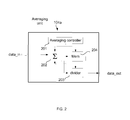
Fig. 3 is a schematic diagram depicting a circuit component performing the dithery pulsing function according to the present invention. -
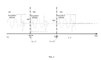
Fig. 4 is a diagram illustrating waveforms of an averaging process with dithery pulsing during an acquisition cycle according to the present invention. -
Fig. 5 is a diagram with an enlarged illustration showing the effect how the acoustic noise is reduced during the averaging process inFig. 4 . contributed to dithery pulsing. - Referring to
Fig. 1 , the preferred embodiment according to the present disclosure used for an ultrasonic instrument is shown to preferably comprise atransducer 106, ananalog channel 101, apulser 102, an analog to digital (A2D)converter 103 and adigital logic device 104.Logic device 104 further comprises anaveraging component 104a and apulser control unit 104b controlling pulser 102. - If a single element is used to transmit and receive, it will be plugged in a transceiver or a
receiver 106 with aswitch 105 closed. If two elements are paired, the receiver will be connected to 106 and a transmitter 107. The usage of probe element shown inFig. 1 is for an exemplary case only. Many other combinations of transmitter, receiver or transceiver and design of single, dual or array elements can be used and the scope of the present disclosure is not restricted in this regard. To start the acquisition,digital logic device 104 usespulser 102 throughpulser control unit 104b to send the first high-frequency pulse to transmitter 107 (and 106 ifswitch 105 is closed). The echoes come back intoanalog channel 101 to be processed with gain and filtering processes, then further fed into analog todigital converter 103. The Digital Logic Device 104 stores the data for future use, such as averaging by anaveraging unit 104a. This whole process is executed for N times for one testing cycle during N acquisition events where N is the averaging factor. After N times of this process, the averaged result is packaged and sent to a display unit (not shown) to display to the operator. - Referring to
Fig.2 , averagingunit 104a according to present disclosure is elaborated. The averaging unit can be designed to work in ways known to those skilled in the art. The following exemplary case is given for illustration purpose and the averaging function is not limited in this regard. In an exemplary case, digitized data from the first pulse is stored directly in amemory 204. On a second pulse, the data from the first pulse is selected in thememory 204 and added by anadder 202 to the current data. The new value is stored inmemory 204. Anaveraging controller 201 selects the right address of the memory for all the pulses. Once the data is collected for N times as specified by the operator, the averaging is done and averagingcontroller 201 selects theright divider 203 that corresponds to N (chosen by the operator). N is preferably a number of a power of two.Fig. 4 later in the present disclosure shows the effect of this averaging in waveform diagrams, giving illustration of the averaging process. - Reference is now made jointly to
Figs. 3 andFig. 4 .Fig. 3 shows howpulser control unit 104b works.Fig. 4 shows the waveforms of a series of acquisition events led by a series of pulsing for a testing cycle. Dithering pulsing is carried out with pulses sent at each time interval T dithered with Dn. - As shown in
Fig. 3 , atiming controller 302 starts the first acquisition using apulser controller 301 to drive thepulser 102 outside the digital logic device. Aregister 304 contains the pulse timeinterval T. ROM 305 contains dither value Dn for the respective acquisition event. Then amain counter 307 starts counting until it reaches the T+Dn for each acquisition event shown inFig. 4 before it re-starts again for a new subsequent acquisition event led by a subsequent pulsing. When T+Dn is achieved byadder 306 which adds the value fromregister 304 and Dn value fromROM 305. The address of the ROM is controlled by apulse counter 303 which is incremented at every pulse. - It is conceivable that it is the same effect whether the
main counter 307 starts to count from To and continue to add nT for each acquisition event, or to restart counting for each acquisition event as above described. For the case of continuous counting, the pulsing points or the dithery pulsing sequence is governed by T0+nT+Dn, wherein n = 1 ∼ N, with n to be sequence number at which the probe is pulsed and N to be averaging factor and Dn is the dither value which much less than T. To is the initial starting point of the whole test. It should be appreciated that the dithery pulsing sequence can be implemented bycounter 307 and timing control mechanism herein presented in different ways which all remain within the framework of present invention. - In one averaging process shown in
Fig. 2 , values Dn preferably dither randomly off zero from pulse to pulse or, at least dither with pairs of positive and negative equal values. There are many ways to make the dithery sequence and assign Dn values. The following two tables give examples of value Dn for an averaging factor of N = 8. As shown in Table-1, dither values can be random numbers. However, with limited averaging factor, it should noted that care should be given so that the sum of all positive dither values should be roughly equal to the sum of negative dither values in one averaging process. In another example as shown in Table-2, dither values can be pairs of negative and positive equal values.Table 1 Random dither value Dn for each pulse Pulser Number n Dn 1 -310ns 2 +280ns 3 -160ns 4 +180ns 5 +80ns 6 -90ns 7 +40ns 8 -40ns Table 2 Dither values in pairs of positive and negative equal values Pulser number D 1 -300ns 2 +300ns 3 -100ns 4 +100ns 5 -300ns 6 +300ns 7 +100ns 8 -100ns - Referring now more specifically to
Fig. 4 , three acquisition events, with three acquisition windows showing waveform of echo signals of from three pulses are illustrated. Acquisition windows are the time frames in which digitized data sample are selected to use in the averaging process. One testing can include N acquisition events, wherein N is the averaging factor as aforementioned. It should be noted that in this context, the same numeral used for respective pulses, waveforms and acquisition windows. For example, pulse 401 and waveform 401 denote to the respective pulse and waveform in the same acquisition event. - During the averaging process, waveform 401 in the respective acquisition window (401) is added to
waveform 402 inacquisition window 402, and so forth for all the pulses. Unfortunately, whenpulse 402 starts, as one can note that there is still acoustic noise (or "tail") from the last pulse 401. The desired signal inside the acquisition window will then be corrupted by the "tail" of 401. This effect is made more obvious inenlarged illustrations Fig. 5 . - Further referring to
Fig. 5 which shows that if the pulses are triggered always at a fixed time interval, which is a multiple of time T, the same part of the tails from the last pulse are added to the echo of the current pulse in the acquisition window. For example, the intersection of thetail 401a and T0 + T, 407a is the same as intersection of 402a and T0 + 2T, 407b. Summing all the acquisition windows at fixed timer intervals will include the echo (desired signal) and unwanted acoustic noise (the remaining "tails"). The closer (in time) the pulses are to each other, the more acoustic noise will remain for the next pulse, due to larger residual amplitude left in the "tails". This is why existing or conventional averaging process adds acoustic noise into the test results. - The dithery pulsing executed by the preferred embodiment shown in
Fig. 3 adds an important novel aspect to conventional averaging and reduces or significantly eliminates acoustic noise in test results. As can be seen inFig. 4 , particularly in an enlarged illustration inFig. 5 , the effect of dithery pulsing by shifting or dithering the time at which the pulses are fired effectively cancels the acoustic noise. Dithering of pulse timing removes the correlation between the pulses and the acoustic noise. This scheme transforms the acoustic noise into white noise. Instead of pulsing at fixed time interval, or at multiple of T, one could pulse at time T+/-Dn where Dn varies at every pulse. - An example is shown in
Fig. 4 . The first three pulses are shown (401, 402 and 403). The number of pulses is determined by the averaging factor N. This factor is usually determined by the operator who takes several factors into consideration, such as the desired precision and the frequency of the acquisitions (PRF). The acoustic noise from the previous pulse is sampled at different times (T-D1 and T+D2). When averaging all the pulses, the remaining acoustic noise will tend to be eliminated, because it is sampled at different moment. - Referring to
Fig. 5 , an exemplary case of the "tails" is illustrated with an enlarged scale. Preferably, the waveforms at each acquisition windows all start to amplitude zero, without the influence of residual acoustic energy from the last pulse. If the pulses would have occurred at a fixed time interval, at every time T, the amplitude of the acoustic noise for the first sampled would be equal in each acquisition window. InFig. 5 , it would be amplitude of +5 forpoint - Although the present invention has been described in relation to particular embodiments thereof, many other variations and modifications and other uses will become apparent to those skilled in the art. It is preferred, therefore, that the present invention be limited not by the specific disclosure herein, but only by the appended claims.
Claims (20)
- A non-destructive inspection or testing (NDT/NDI) device configured for inspecting a test object, comprising:a probe configured for pulsing a test object during a testing cycle at a testing location with N pulses to produce and receive N sets of wave responses, and to produce therefrom N sets of electric echo signals;at least one analog to digital converter configured to digitize the N sets of echo signals and to produce therefrom N sets of digitized signal samples, which correspond respectively to N sets of acquired signal samples and N sets of noise signal samples;a digital logic device, having a data processing unit configured to execute an averaging process by which the N sets of signal samples are summed and averaged to produce a final testing result;wherein the digital logic device further comprises a pulser control unit configured to control the pulsing according to a dithery pulsing sequence by which the probe is pulsed in a dithery pattern between one pulse and another so that the combination effect of the N sets of the noise signal samples is decimated during the averaging process and in the testing result.
- The device of claim 1, wherein N is an averaging factor used by the digital logic device for the averaging process.
- The device of claim 1, wherein the digital logic device further comprises an averaging unit for executing the averaging process, the averaging unit further including an averaging controller, a digital memory, an adder and a divider.
- The device of claim 1, wherein the pulser control unit further comprises a timing controller, a pulser counter, a timing adder, a main counter and pulser controller to apply the dithery pulsing.
- The device of claim 1, wherein the dithery pulsing sequence is governed by T0+nT+Dn, wherein n = 1 ∼ N, with n to be sequence number at which the probe is pulsed and N to be the averaging factor and Dn are dither values and are much less than T.
- The device of claim 5, wherein Dn are random and small numbers around zero.
- The device of claim 5, wherein Dn are pairs of small positive and negative numbers very small in value comparing to T.
- The device of claim 1, wherein the probe includes a single element ultrasonic transmitter.
- The device of claim 1, wherein the probe includes a single element transceiver.
- The device of claim 1, wherein the probe is a dual element probe.
- The device of claim 1, wherein the probe is a phased array probe.
- A method of pulsing a non-destructive inspection or testing (NDT/NDI) device having a probe configured for pulsing a test object during a testing cycle, the method comprises the steps of:pulsing the probe with N pulses according to a pulsing sequence,causing the probe to receive N sets of wave responses, and to produce therefrom N sets of electric echo signals;digitizing the N sets of echo signals to produce N sets of digitized signal samples, which correspond respectively to N sets of acquired signal samples and N sets of noise signal samples;averaging said N sets of acquired signal samples;wherein the pulsing sequence has a dithery pattern between one pulse and another so that the combination effect of the N sets of the noise signal samples is decimated during the averaging step and in the testing result.
- The method of claim 12, wherein the steps of pulsing, digitizing and averaging are executed by a digital logic device.
- The method of claim 13, wherein the digital logic device further comprises an averaging unit for executing the averaging process, the averaging unit further including an averaging controller, a digital memory, an adder and a divider.
- The method claim 13, wherein the logic device further comprising a pulser control unit which further comprises a timing controller, a pulser counter, a timing adder, a main counter and pulser controller to apply the dithery pulsing.
- The method claim 12, wherein the dithery pulsing sequence is governed by T0+nT+Dn, wherein n = 1 ∼ N, with n to be sequence number at which the probe is pulsed and N to be averaging factor and Dn are dither values and are much less than T.
- The method claim 5, wherein Dn are random and small numbers around zero.
- The method claim 5, wherein Dun are pairs of small positive and negative very small in value.
- The method claim 1, wherein the probe includes a single element ultrasonic probe.
- The method claim 1, wherein the probe is a multiple or array element ultrasonic probe.
Applications Claiming Priority (1)
| Application Number | Priority Date | Filing Date | Title |
|---|---|---|---|
| US13/654,969 US9638673B2 (en) | 2012-10-18 | 2012-10-18 | Ultrasonic testing instrument with dithery pulsing |
Publications (2)
| Publication Number | Publication Date |
|---|---|
| EP2722667A1 true EP2722667A1 (en) | 2014-04-23 |
| EP2722667B1 EP2722667B1 (en) | 2024-05-08 |
Family
ID=49322296
Family Applications (1)
| Application Number | Title | Priority Date | Filing Date |
|---|---|---|---|
| EP13188350.6A Active EP2722667B1 (en) | 2012-10-18 | 2013-10-11 | An ultrasonic testing instrument with dithery pulsing |
Country Status (3)
| Country | Link |
|---|---|
| US (1) | US9638673B2 (en) |
| EP (1) | EP2722667B1 (en) |
| CN (1) | CN103808808B (en) |
Cited By (1)
| Publication number | Priority date | Publication date | Assignee | Title |
|---|---|---|---|---|
| WO2021016164A1 (en) * | 2019-07-19 | 2021-01-28 | Mayo Foundation For Medical Education And Research | Systems and methods for ultrasound attenuation coefficient estimation |
Families Citing this family (2)
| Publication number | Priority date | Publication date | Assignee | Title |
|---|---|---|---|---|
| US10672046B2 (en) * | 2012-12-31 | 2020-06-02 | Baker Hughes, A Ge Company, Llc | Systems and methods for non-destructive testing online stores |
| US10076802B2 (en) * | 2014-12-19 | 2018-09-18 | Illinois Tool Works Inc. | Electric arc start systems and methods |
Citations (4)
| Publication number | Priority date | Publication date | Assignee | Title |
|---|---|---|---|---|
| US3557354A (en) | 1966-06-13 | 1971-01-19 | Hewlett Packard Co | Signal-to-noise ratio enhancement methods and means |
| US4825379A (en) * | 1986-08-29 | 1989-04-25 | Tektronix, Inc. | Method and apparatus for processing waveform records for jitter elimination prior to averaging in determining signal to noise ratio |
| US5671154A (en) * | 1993-06-07 | 1997-09-23 | Nkk Corporation | Signal processing method and signal processing device for ultrasonic inspection apparatus |
| US7254494B2 (en) | 2002-11-25 | 2007-08-07 | Instromet Ultrasonics B.V. | Ultrasonic signal processing method and applications thereof |
Family Cites Families (10)
| Publication number | Priority date | Publication date | Assignee | Title |
|---|---|---|---|---|
| US5059959A (en) * | 1985-06-03 | 1991-10-22 | Seven Oaks Corporation | Cursor positioning method and apparatus |
| US5811682A (en) * | 1995-12-13 | 1998-09-22 | Ebara Corporation | Electromagnetic acoustic transducer EMAT and inspection system with EMAR |
| US6204663B1 (en) * | 1997-03-26 | 2001-03-20 | Numar Corporation | Pulse sequence and method for suppression of magneto-acoustic artifacts in NMR data |
| US6462705B1 (en) * | 2000-08-17 | 2002-10-08 | Mcewan Technologies, Llc | Spread spectrum radar clock |
| JP4431926B2 (en) * | 2000-12-26 | 2010-03-17 | 新日本製鐵株式会社 | Ultrasonic flaw detection apparatus and ultrasonic flaw detection method |
| DE10123237B4 (en) * | 2001-05-12 | 2005-11-17 | Eads Deutschland Gmbh | Non-destructive ultrasonic test method for damage detection, as well as testing device for carrying out the same |
| JP2007046913A (en) * | 2005-08-05 | 2007-02-22 | Mitsubishi Heavy Ind Ltd | Welded structure flaw detection testing method, and steel welded structure flaw detector |
| US8156813B2 (en) * | 2009-12-03 | 2012-04-17 | Olympus Ndt Inc. | High dynamic range NDT/NDI inspection device with selective noise averaging |
| JP5600980B2 (en) * | 2010-03-19 | 2014-10-08 | Jfeスチール株式会社 | Ultrasonic measurement method and ultrasonic measurement apparatus |
| CN103995055A (en) * | 2014-05-23 | 2014-08-20 | 中国石油化工股份有限公司 | Screening method for eliminating noise interfered data of acoustic emission testing on large-size storage tank |
-
2012
- 2012-10-18 US US13/654,969 patent/US9638673B2/en active Active
-
2013
- 2013-10-11 EP EP13188350.6A patent/EP2722667B1/en active Active
- 2013-10-18 CN CN201310492258.3A patent/CN103808808B/en active Active
Patent Citations (4)
| Publication number | Priority date | Publication date | Assignee | Title |
|---|---|---|---|---|
| US3557354A (en) | 1966-06-13 | 1971-01-19 | Hewlett Packard Co | Signal-to-noise ratio enhancement methods and means |
| US4825379A (en) * | 1986-08-29 | 1989-04-25 | Tektronix, Inc. | Method and apparatus for processing waveform records for jitter elimination prior to averaging in determining signal to noise ratio |
| US5671154A (en) * | 1993-06-07 | 1997-09-23 | Nkk Corporation | Signal processing method and signal processing device for ultrasonic inspection apparatus |
| US7254494B2 (en) | 2002-11-25 | 2007-08-07 | Instromet Ultrasonics B.V. | Ultrasonic signal processing method and applications thereof |
Cited By (1)
| Publication number | Priority date | Publication date | Assignee | Title |
|---|---|---|---|---|
| WO2021016164A1 (en) * | 2019-07-19 | 2021-01-28 | Mayo Foundation For Medical Education And Research | Systems and methods for ultrasound attenuation coefficient estimation |
Also Published As
| Publication number | Publication date |
|---|---|
| EP2722667B1 (en) | 2024-05-08 |
| US9638673B2 (en) | 2017-05-02 |
| CN103808808B (en) | 2017-04-12 |
| CN103808808A (en) | 2014-05-21 |
| US20140109675A1 (en) | 2014-04-24 |
Similar Documents
| Publication | Publication Date | Title |
|---|---|---|
| US8245577B2 (en) | Pulse period jitter for artifact detection or reduction in ultrasound imaging | |
| CN1218174C (en) | Supersonic imaging system with ultrasound formed by using single-pole or two-pole coding excited wave beam | |
| US5984869A (en) | Method and apparatus for ultrasonic beamforming using golay-coded excitation | |
| KR101552427B1 (en) | Speckle Reduction Apparatus In Ultrasound Imaging | |
| JP2005536309A (en) | System and method for improved harmonic imaging | |
| JP3352098B2 (en) | Object inspection system by ultrasonic echograph | |
| CN101400994B (en) | Digital time variable gain circuit for non-destructive test instrument | |
| EP2722667B1 (en) | An ultrasonic testing instrument with dithery pulsing | |
| JP2007222390A (en) | Ultrasonic diagnostic equipment | |
| WO2013148859A1 (en) | Ultrasonic receiver front-end | |
| US20200080969A1 (en) | Method for acquiring signals by ultrasound probing, corresponding computer program and ultrasound probing device | |
| US20160238569A1 (en) | Detecting method for improving resolution of area array probe | |
| CN106137252B (en) | Contrast agent sensitive medical ultrasound imaging | |
| EP1785983B1 (en) | Ultrasonic imaging method and apparatus | |
| RU2308047C2 (en) | Method for pulse interference protection at detection of composite radar signals | |
| White et al. | Pseudo random binary sequence techniques for ultrasonic NDE of high loss materials | |
| RU2677835C1 (en) | Hydro-acoustic tone signals resolution method | |
| EP2761286A1 (en) | Method for processing an ultrasonic analog signal, digital signal processing unit and ultrasonic inspection device | |
| JP2013029396A (en) | Ultrasonic inspection device | |
| JP2669204B2 (en) | Exploration equipment | |
| JPH04231889A (en) | Device for removing fixed echo in ultrasonic echo graph | |
| Avdal et al. | Effects of reverberations and clutter filtering in pulsed Doppler using sparse sequences | |
| RU2293358C1 (en) | Mode of detection of a sonar echo-signal | |
| RU2828233C1 (en) | Echo sounder | |
| RU2520959C1 (en) | Control over rock massif strain-stress behaviour variation |
Legal Events
| Date | Code | Title | Description |
|---|---|---|---|
| PUAI | Public reference made under article 153(3) epc to a published international application that has entered the european phase |
Free format text: ORIGINAL CODE: 0009012 |
|
| AK | Designated contracting states |
Kind code of ref document: A1 Designated state(s): AL AT BE BG CH CY CZ DE DK EE ES FI FR GB GR HR HU IE IS IT LI LT LU LV MC MK MT NL NO PL PT RO RS SE SI SK SM TR |
|
| AX | Request for extension of the european patent |
Extension state: BA ME |
|
| 17P | Request for examination filed |
Effective date: 20141023 |
|
| RBV | Designated contracting states (corrected) |
Designated state(s): AL AT BE BG CH CY CZ DE DK EE ES FI FR GB GR HR HU IE IS IT LI LT LU LV MC MK MT NL NO PL PT RO RS SE SI SK SM TR |
|
| STAA | Information on the status of an ep patent application or granted ep patent |
Free format text: STATUS: EXAMINATION IS IN PROGRESS |
|
| 17Q | First examination report despatched |
Effective date: 20180409 |
|
| GRAP | Despatch of communication of intention to grant a patent |
Free format text: ORIGINAL CODE: EPIDOSNIGR1 |
|
| STAA | Information on the status of an ep patent application or granted ep patent |
Free format text: STATUS: GRANT OF PATENT IS INTENDED |
|
| INTG | Intention to grant announced |
Effective date: 20231215 |
|
| GRAS | Grant fee paid |
Free format text: ORIGINAL CODE: EPIDOSNIGR3 |
|
| GRAA | (expected) grant |
Free format text: ORIGINAL CODE: 0009210 |
|
| STAA | Information on the status of an ep patent application or granted ep patent |
Free format text: STATUS: THE PATENT HAS BEEN GRANTED |
|
| AK | Designated contracting states |
Kind code of ref document: B1 Designated state(s): AL AT BE BG CH CY CZ DE DK EE ES FI FR GB GR HR HU IE IS IT LI LT LU LV MC MK MT NL NO PL PT RO RS SE SI SK SM TR |
|
| REG | Reference to a national code |
Ref country code: GB Ref legal event code: FG4D |
|
| REG | Reference to a national code |
Ref country code: CH Ref legal event code: EP |
|
| REG | Reference to a national code |
Ref country code: DE Ref legal event code: R096 Ref document number: 602013085689 Country of ref document: DE |
|
| REG | Reference to a national code |
Ref country code: IE Ref legal event code: FG4D |
|
| REG | Reference to a national code |
Ref country code: DE Ref legal event code: R081 Ref document number: 602013085689 Country of ref document: DE Owner name: EVIDENT SCIENTIFIC, INC., WALTHAM, US Free format text: FORMER OWNER: OLYMPUS NDT, INC., WALTHAM, MA, US |
|
| REG | Reference to a national code |
Ref country code: LT Ref legal event code: MG9D |
|
| RAP2 | Party data changed (patent owner data changed or rights of a patent transferred) |
Owner name: EVIDENT SCIENTIFIC, INC. |
|
| REG | Reference to a national code |
Ref country code: NL Ref legal event code: MP Effective date: 20240508 |
|
| REG | Reference to a national code |
Ref country code: GB Ref legal event code: 732E Free format text: REGISTERED BETWEEN 20240905 AND 20240911 |
|
| PG25 | Lapsed in a contracting state [announced via postgrant information from national office to epo] |
Ref country code: IS Free format text: LAPSE BECAUSE OF FAILURE TO SUBMIT A TRANSLATION OF THE DESCRIPTION OR TO PAY THE FEE WITHIN THE PRESCRIBED TIME-LIMIT Effective date: 20240908 |
|
| PG25 | Lapsed in a contracting state [announced via postgrant information from national office to epo] |
Ref country code: BG Free format text: LAPSE BECAUSE OF FAILURE TO SUBMIT A TRANSLATION OF THE DESCRIPTION OR TO PAY THE FEE WITHIN THE PRESCRIBED TIME-LIMIT Effective date: 20240508 |
|
| PG25 | Lapsed in a contracting state [announced via postgrant information from national office to epo] |
Ref country code: FI Free format text: LAPSE BECAUSE OF FAILURE TO SUBMIT A TRANSLATION OF THE DESCRIPTION OR TO PAY THE FEE WITHIN THE PRESCRIBED TIME-LIMIT Effective date: 20240508 Ref country code: HR Free format text: LAPSE BECAUSE OF FAILURE TO SUBMIT A TRANSLATION OF THE DESCRIPTION OR TO PAY THE FEE WITHIN THE PRESCRIBED TIME-LIMIT Effective date: 20240508 |
|
| PG25 | Lapsed in a contracting state [announced via postgrant information from national office to epo] |
Ref country code: GR Free format text: LAPSE BECAUSE OF FAILURE TO SUBMIT A TRANSLATION OF THE DESCRIPTION OR TO PAY THE FEE WITHIN THE PRESCRIBED TIME-LIMIT Effective date: 20240809 |
|
| PG25 | Lapsed in a contracting state [announced via postgrant information from national office to epo] |
Ref country code: PT Free format text: LAPSE BECAUSE OF FAILURE TO SUBMIT A TRANSLATION OF THE DESCRIPTION OR TO PAY THE FEE WITHIN THE PRESCRIBED TIME-LIMIT Effective date: 20240909 |
|
| REG | Reference to a national code |
Ref country code: AT Ref legal event code: MK05 Ref document number: 1685384 Country of ref document: AT Kind code of ref document: T Effective date: 20240508 |
|
| PG25 | Lapsed in a contracting state [announced via postgrant information from national office to epo] |
Ref country code: NL Free format text: LAPSE BECAUSE OF FAILURE TO SUBMIT A TRANSLATION OF THE DESCRIPTION OR TO PAY THE FEE WITHIN THE PRESCRIBED TIME-LIMIT Effective date: 20240508 |
|
| PG25 | Lapsed in a contracting state [announced via postgrant information from national office to epo] |
Ref country code: ES Free format text: LAPSE BECAUSE OF FAILURE TO SUBMIT A TRANSLATION OF THE DESCRIPTION OR TO PAY THE FEE WITHIN THE PRESCRIBED TIME-LIMIT Effective date: 20240508 |
|
| PG25 | Lapsed in a contracting state [announced via postgrant information from national office to epo] |
Ref country code: AT Free format text: LAPSE BECAUSE OF FAILURE TO SUBMIT A TRANSLATION OF THE DESCRIPTION OR TO PAY THE FEE WITHIN THE PRESCRIBED TIME-LIMIT Effective date: 20240508 |
|
| PG25 | Lapsed in a contracting state [announced via postgrant information from national office to epo] |
Ref country code: PL Free format text: LAPSE BECAUSE OF FAILURE TO SUBMIT A TRANSLATION OF THE DESCRIPTION OR TO PAY THE FEE WITHIN THE PRESCRIBED TIME-LIMIT Effective date: 20240508 |
|
| PG25 | Lapsed in a contracting state [announced via postgrant information from national office to epo] |
Ref country code: LV Free format text: LAPSE BECAUSE OF FAILURE TO SUBMIT A TRANSLATION OF THE DESCRIPTION OR TO PAY THE FEE WITHIN THE PRESCRIBED TIME-LIMIT Effective date: 20240508 |
|
| PG25 | Lapsed in a contracting state [announced via postgrant information from national office to epo] |
Ref country code: PT Free format text: LAPSE BECAUSE OF FAILURE TO SUBMIT A TRANSLATION OF THE DESCRIPTION OR TO PAY THE FEE WITHIN THE PRESCRIBED TIME-LIMIT Effective date: 20240909 Ref country code: PL Free format text: LAPSE BECAUSE OF FAILURE TO SUBMIT A TRANSLATION OF THE DESCRIPTION OR TO PAY THE FEE WITHIN THE PRESCRIBED TIME-LIMIT Effective date: 20240508 Ref country code: NO Free format text: LAPSE BECAUSE OF FAILURE TO SUBMIT A TRANSLATION OF THE DESCRIPTION OR TO PAY THE FEE WITHIN THE PRESCRIBED TIME-LIMIT Effective date: 20240808 Ref country code: NL Free format text: LAPSE BECAUSE OF FAILURE TO SUBMIT A TRANSLATION OF THE DESCRIPTION OR TO PAY THE FEE WITHIN THE PRESCRIBED TIME-LIMIT Effective date: 20240508 Ref country code: LV Free format text: LAPSE BECAUSE OF FAILURE TO SUBMIT A TRANSLATION OF THE DESCRIPTION OR TO PAY THE FEE WITHIN THE PRESCRIBED TIME-LIMIT Effective date: 20240508 Ref country code: IS Free format text: LAPSE BECAUSE OF FAILURE TO SUBMIT A TRANSLATION OF THE DESCRIPTION OR TO PAY THE FEE WITHIN THE PRESCRIBED TIME-LIMIT Effective date: 20240908 Ref country code: HR Free format text: LAPSE BECAUSE OF FAILURE TO SUBMIT A TRANSLATION OF THE DESCRIPTION OR TO PAY THE FEE WITHIN THE PRESCRIBED TIME-LIMIT Effective date: 20240508 Ref country code: GR Free format text: LAPSE BECAUSE OF FAILURE TO SUBMIT A TRANSLATION OF THE DESCRIPTION OR TO PAY THE FEE WITHIN THE PRESCRIBED TIME-LIMIT Effective date: 20240809 Ref country code: FI Free format text: LAPSE BECAUSE OF FAILURE TO SUBMIT A TRANSLATION OF THE DESCRIPTION OR TO PAY THE FEE WITHIN THE PRESCRIBED TIME-LIMIT Effective date: 20240508 Ref country code: ES Free format text: LAPSE BECAUSE OF FAILURE TO SUBMIT A TRANSLATION OF THE DESCRIPTION OR TO PAY THE FEE WITHIN THE PRESCRIBED TIME-LIMIT Effective date: 20240508 Ref country code: BG Free format text: LAPSE BECAUSE OF FAILURE TO SUBMIT A TRANSLATION OF THE DESCRIPTION OR TO PAY THE FEE WITHIN THE PRESCRIBED TIME-LIMIT Effective date: 20240508 Ref country code: AT Free format text: LAPSE BECAUSE OF FAILURE TO SUBMIT A TRANSLATION OF THE DESCRIPTION OR TO PAY THE FEE WITHIN THE PRESCRIBED TIME-LIMIT Effective date: 20240508 Ref country code: RS Free format text: LAPSE BECAUSE OF FAILURE TO SUBMIT A TRANSLATION OF THE DESCRIPTION OR TO PAY THE FEE WITHIN THE PRESCRIBED TIME-LIMIT Effective date: 20240808 |
|
| PG25 | Lapsed in a contracting state [announced via postgrant information from national office to epo] |
Ref country code: DK Free format text: LAPSE BECAUSE OF FAILURE TO SUBMIT A TRANSLATION OF THE DESCRIPTION OR TO PAY THE FEE WITHIN THE PRESCRIBED TIME-LIMIT Effective date: 20240508 |
|
| PG25 | Lapsed in a contracting state [announced via postgrant information from national office to epo] |
Ref country code: EE Free format text: LAPSE BECAUSE OF FAILURE TO SUBMIT A TRANSLATION OF THE DESCRIPTION OR TO PAY THE FEE WITHIN THE PRESCRIBED TIME-LIMIT Effective date: 20240508 |
|
| PG25 | Lapsed in a contracting state [announced via postgrant information from national office to epo] |
Ref country code: CZ Free format text: LAPSE BECAUSE OF FAILURE TO SUBMIT A TRANSLATION OF THE DESCRIPTION OR TO PAY THE FEE WITHIN THE PRESCRIBED TIME-LIMIT Effective date: 20240508 |
|
| PG25 | Lapsed in a contracting state [announced via postgrant information from national office to epo] |
Ref country code: SK Free format text: LAPSE BECAUSE OF FAILURE TO SUBMIT A TRANSLATION OF THE DESCRIPTION OR TO PAY THE FEE WITHIN THE PRESCRIBED TIME-LIMIT Effective date: 20240508 Ref country code: RO Free format text: LAPSE BECAUSE OF FAILURE TO SUBMIT A TRANSLATION OF THE DESCRIPTION OR TO PAY THE FEE WITHIN THE PRESCRIBED TIME-LIMIT Effective date: 20240508 |
|
| PG25 | Lapsed in a contracting state [announced via postgrant information from national office to epo] |
Ref country code: SM Free format text: LAPSE BECAUSE OF FAILURE TO SUBMIT A TRANSLATION OF THE DESCRIPTION OR TO PAY THE FEE WITHIN THE PRESCRIBED TIME-LIMIT Effective date: 20240508 |
|
| PG25 | Lapsed in a contracting state [announced via postgrant information from national office to epo] |
Ref country code: SM Free format text: LAPSE BECAUSE OF FAILURE TO SUBMIT A TRANSLATION OF THE DESCRIPTION OR TO PAY THE FEE WITHIN THE PRESCRIBED TIME-LIMIT Effective date: 20240508 Ref country code: SK Free format text: LAPSE BECAUSE OF FAILURE TO SUBMIT A TRANSLATION OF THE DESCRIPTION OR TO PAY THE FEE WITHIN THE PRESCRIBED TIME-LIMIT Effective date: 20240508 Ref country code: RO Free format text: LAPSE BECAUSE OF FAILURE TO SUBMIT A TRANSLATION OF THE DESCRIPTION OR TO PAY THE FEE WITHIN THE PRESCRIBED TIME-LIMIT Effective date: 20240508 Ref country code: EE Free format text: LAPSE BECAUSE OF FAILURE TO SUBMIT A TRANSLATION OF THE DESCRIPTION OR TO PAY THE FEE WITHIN THE PRESCRIBED TIME-LIMIT Effective date: 20240508 Ref country code: DK Free format text: LAPSE BECAUSE OF FAILURE TO SUBMIT A TRANSLATION OF THE DESCRIPTION OR TO PAY THE FEE WITHIN THE PRESCRIBED TIME-LIMIT Effective date: 20240508 Ref country code: CZ Free format text: LAPSE BECAUSE OF FAILURE TO SUBMIT A TRANSLATION OF THE DESCRIPTION OR TO PAY THE FEE WITHIN THE PRESCRIBED TIME-LIMIT Effective date: 20240508 |
|
| PG25 | Lapsed in a contracting state [announced via postgrant information from national office to epo] |
Ref country code: IT Free format text: LAPSE BECAUSE OF FAILURE TO SUBMIT A TRANSLATION OF THE DESCRIPTION OR TO PAY THE FEE WITHIN THE PRESCRIBED TIME-LIMIT Effective date: 20240508 |
|
| REG | Reference to a national code |
Ref country code: DE Ref legal event code: R097 Ref document number: 602013085689 Country of ref document: DE |
|
| PLBE | No opposition filed within time limit |
Free format text: ORIGINAL CODE: 0009261 |
|
| STAA | Information on the status of an ep patent application or granted ep patent |
Free format text: STATUS: NO OPPOSITION FILED WITHIN TIME LIMIT |
|
| 26N | No opposition filed |
Effective date: 20250211 |
|
| PG25 | Lapsed in a contracting state [announced via postgrant information from national office to epo] |
Ref country code: SI Free format text: LAPSE BECAUSE OF FAILURE TO SUBMIT A TRANSLATION OF THE DESCRIPTION OR TO PAY THE FEE WITHIN THE PRESCRIBED TIME-LIMIT Effective date: 20240508 |
|
| REG | Reference to a national code |
Ref country code: CH Ref legal event code: PL |
|
| PG25 | Lapsed in a contracting state [announced via postgrant information from national office to epo] |
Ref country code: MC Free format text: LAPSE BECAUSE OF FAILURE TO SUBMIT A TRANSLATION OF THE DESCRIPTION OR TO PAY THE FEE WITHIN THE PRESCRIBED TIME-LIMIT Effective date: 20240508 |
|
| PG25 | Lapsed in a contracting state [announced via postgrant information from national office to epo] |
Ref country code: LU Free format text: LAPSE BECAUSE OF NON-PAYMENT OF DUE FEES Effective date: 20241011 Ref country code: BE Free format text: LAPSE BECAUSE OF NON-PAYMENT OF DUE FEES Effective date: 20241031 |
|
| PG25 | Lapsed in a contracting state [announced via postgrant information from national office to epo] |
Ref country code: CH Free format text: LAPSE BECAUSE OF NON-PAYMENT OF DUE FEES Effective date: 20241031 |
|
| REG | Reference to a national code |
Ref country code: BE Ref legal event code: MM Effective date: 20241031 |
|
| PG25 | Lapsed in a contracting state [announced via postgrant information from national office to epo] |
Ref country code: SE Free format text: LAPSE BECAUSE OF FAILURE TO SUBMIT A TRANSLATION OF THE DESCRIPTION OR TO PAY THE FEE WITHIN THE PRESCRIBED TIME-LIMIT Effective date: 20240508 |
|
| PG25 | Lapsed in a contracting state [announced via postgrant information from national office to epo] |
Ref country code: IE Free format text: LAPSE BECAUSE OF NON-PAYMENT OF DUE FEES Effective date: 20241011 |
|
| PGFP | Annual fee paid to national office [announced via postgrant information from national office to epo] |
Ref country code: DE Payment date: 20251029 Year of fee payment: 13 |
|
| PGFP | Annual fee paid to national office [announced via postgrant information from national office to epo] |
Ref country code: GB Payment date: 20251027 Year of fee payment: 13 |
|
| PGFP | Annual fee paid to national office [announced via postgrant information from national office to epo] |
Ref country code: FR Payment date: 20251027 Year of fee payment: 13 |
|
| PG25 | Lapsed in a contracting state [announced via postgrant information from national office to epo] |
Ref country code: CY Free format text: LAPSE BECAUSE OF FAILURE TO SUBMIT A TRANSLATION OF THE DESCRIPTION OR TO PAY THE FEE WITHIN THE PRESCRIBED TIME-LIMIT; INVALID AB INITIO Effective date: 20131011 |
|
| PG25 | Lapsed in a contracting state [announced via postgrant information from national office to epo] |
Ref country code: HU Free format text: LAPSE BECAUSE OF FAILURE TO SUBMIT A TRANSLATION OF THE DESCRIPTION OR TO PAY THE FEE WITHIN THE PRESCRIBED TIME-LIMIT; INVALID AB INITIO Effective date: 20131011 |
|
| PG25 | Lapsed in a contracting state [announced via postgrant information from national office to epo] |
Ref country code: TR Free format text: LAPSE BECAUSE OF FAILURE TO SUBMIT A TRANSLATION OF THE DESCRIPTION OR TO PAY THE FEE WITHIN THE PRESCRIBED TIME-LIMIT Effective date: 20240508 |
|
| PG25 | Lapsed in a contracting state [announced via postgrant information from national office to epo] |
Ref country code: LT Free format text: LAPSE BECAUSE OF FAILURE TO SUBMIT A TRANSLATION OF THE DESCRIPTION OR TO PAY THE FEE WITHIN THE PRESCRIBED TIME-LIMIT Effective date: 20240508 |