EP2721193B1 - Method for manufacturing a barrier layer on a flexible substrate - Google Patents
Method for manufacturing a barrier layer on a flexible substrate Download PDFInfo
- Publication number
- EP2721193B1 EP2721193B1 EP12719037.9A EP12719037A EP2721193B1 EP 2721193 B1 EP2721193 B1 EP 2721193B1 EP 12719037 A EP12719037 A EP 12719037A EP 2721193 B1 EP2721193 B1 EP 2721193B1
- Authority
- EP
- European Patent Office
- Prior art keywords
- substrate
- electrodes
- plasma
- layer
- treatment space
- Prior art date
- Legal status (The legal status is an assumption and is not a legal conclusion. Google has not performed a legal analysis and makes no representation as to the accuracy of the status listed.)
- Not-in-force
Links
Images

Classifications
-
- C—CHEMISTRY; METALLURGY
- C23—COATING METALLIC MATERIAL; COATING MATERIAL WITH METALLIC MATERIAL; CHEMICAL SURFACE TREATMENT; DIFFUSION TREATMENT OF METALLIC MATERIAL; COATING BY VACUUM EVAPORATION, BY SPUTTERING, BY ION IMPLANTATION OR BY CHEMICAL VAPOUR DEPOSITION, IN GENERAL; INHIBITING CORROSION OF METALLIC MATERIAL OR INCRUSTATION IN GENERAL
- C23C—COATING METALLIC MATERIAL; COATING MATERIAL WITH METALLIC MATERIAL; SURFACE TREATMENT OF METALLIC MATERIAL BY DIFFUSION INTO THE SURFACE, BY CHEMICAL CONVERSION OR SUBSTITUTION; COATING BY VACUUM EVAPORATION, BY SPUTTERING, BY ION IMPLANTATION OR BY CHEMICAL VAPOUR DEPOSITION, IN GENERAL
- C23C16/00—Chemical coating by decomposition of gaseous compounds, without leaving reaction products of surface material in the coating, i.e. chemical vapour deposition [CVD] processes
- C23C16/22—Chemical coating by decomposition of gaseous compounds, without leaving reaction products of surface material in the coating, i.e. chemical vapour deposition [CVD] processes characterised by the deposition of inorganic material, other than metallic material
- C23C16/30—Deposition of compounds, mixtures or solid solutions, e.g. borides, carbides, nitrides
- C23C16/40—Oxides
- C23C16/401—Oxides containing silicon
-
- H—ELECTRICITY
- H10—SEMICONDUCTOR DEVICES; ELECTRIC SOLID-STATE DEVICES NOT OTHERWISE PROVIDED FOR
- H10P—GENERIC PROCESSES OR APPARATUS FOR THE MANUFACTURE OR TREATMENT OF DEVICES COVERED BY CLASS H10
- H10P14/00—Formation of materials, e.g. in the shape of layers or pillars
- H10P14/60—Formation of materials, e.g. in the shape of layers or pillars of insulating materials
- H10P14/63—Formation of materials, e.g. in the shape of layers or pillars of insulating materials characterised by the formation processes
- H10P14/6302—Non-deposition formation processes
- H10P14/6316—Formation by nitridation, e.g. nitridation of the substrate
-
- C—CHEMISTRY; METALLURGY
- C23—COATING METALLIC MATERIAL; COATING MATERIAL WITH METALLIC MATERIAL; CHEMICAL SURFACE TREATMENT; DIFFUSION TREATMENT OF METALLIC MATERIAL; COATING BY VACUUM EVAPORATION, BY SPUTTERING, BY ION IMPLANTATION OR BY CHEMICAL VAPOUR DEPOSITION, IN GENERAL; INHIBITING CORROSION OF METALLIC MATERIAL OR INCRUSTATION IN GENERAL
- C23C—COATING METALLIC MATERIAL; COATING MATERIAL WITH METALLIC MATERIAL; SURFACE TREATMENT OF METALLIC MATERIAL BY DIFFUSION INTO THE SURFACE, BY CHEMICAL CONVERSION OR SUBSTITUTION; COATING BY VACUUM EVAPORATION, BY SPUTTERING, BY ION IMPLANTATION OR BY CHEMICAL VAPOUR DEPOSITION, IN GENERAL
- C23C16/00—Chemical coating by decomposition of gaseous compounds, without leaving reaction products of surface material in the coating, i.e. chemical vapour deposition [CVD] processes
- C23C16/56—After-treatment
-
- H—ELECTRICITY
- H01—ELECTRIC ELEMENTS
- H01J—ELECTRIC DISCHARGE TUBES OR DISCHARGE LAMPS
- H01J37/00—Discharge tubes with provision for introducing objects or material to be exposed to the discharge, e.g. for the purpose of examination or processing thereof
- H01J37/32—Gas-filled discharge tubes
- H01J37/32009—Arrangements for generation of plasma specially adapted for examination or treatment of objects, e.g. plasma sources
- H01J37/32018—Glow discharge
-
- H—ELECTRICITY
- H10—SEMICONDUCTOR DEVICES; ELECTRIC SOLID-STATE DEVICES NOT OTHERWISE PROVIDED FOR
- H10D—INORGANIC ELECTRIC SEMICONDUCTOR DEVICES
- H10D64/00—Electrodes of devices having potential barriers
- H10D64/118—Electrodes comprising insulating layers having particular dielectric or electrostatic properties, e.g. having static charges
-
- H—ELECTRICITY
- H10—SEMICONDUCTOR DEVICES; ELECTRIC SOLID-STATE DEVICES NOT OTHERWISE PROVIDED FOR
- H10K—ORGANIC ELECTRIC SOLID-STATE DEVICES
- H10K77/00—Constructional details of devices covered by this subclass and not covered by groups H10K10/80, H10K30/80, H10K50/80 or H10K59/80
- H10K77/10—Substrates, e.g. flexible substrates
- H10K77/111—Flexible substrates
-
- H—ELECTRICITY
- H10—SEMICONDUCTOR DEVICES; ELECTRIC SOLID-STATE DEVICES NOT OTHERWISE PROVIDED FOR
- H10P—GENERIC PROCESSES OR APPARATUS FOR THE MANUFACTURE OR TREATMENT OF DEVICES COVERED BY CLASS H10
- H10P14/00—Formation of materials, e.g. in the shape of layers or pillars
- H10P14/60—Formation of materials, e.g. in the shape of layers or pillars of insulating materials
- H10P14/65—Formation of materials, e.g. in the shape of layers or pillars of insulating materials characterised by treatments performed before or after the formation of the materials
- H10P14/6516—Formation of materials, e.g. in the shape of layers or pillars of insulating materials characterised by treatments performed before or after the formation of the materials of treatments performed after formation of the materials
- H10P14/6518—Formation of materials, e.g. in the shape of layers or pillars of insulating materials characterised by treatments performed before or after the formation of the materials of treatments performed after formation of the materials by introduction of substances into an already-existing insulating layer
- H10P14/6524—Formation of materials, e.g. in the shape of layers or pillars of insulating materials characterised by treatments performed before or after the formation of the materials of treatments performed after formation of the materials by introduction of substances into an already-existing insulating layer the substance being nitrogen
- H10P14/6526—Formation of materials, e.g. in the shape of layers or pillars of insulating materials characterised by treatments performed before or after the formation of the materials of treatments performed after formation of the materials by introduction of substances into an already-existing insulating layer the substance being nitrogen introduced into an oxide material, e.g. changing SiO to SiON
-
- H—ELECTRICITY
- H10—SEMICONDUCTOR DEVICES; ELECTRIC SOLID-STATE DEVICES NOT OTHERWISE PROVIDED FOR
- H10P—GENERIC PROCESSES OR APPARATUS FOR THE MANUFACTURE OR TREATMENT OF DEVICES COVERED BY CLASS H10
- H10P14/00—Formation of materials, e.g. in the shape of layers or pillars
- H10P14/60—Formation of materials, e.g. in the shape of layers or pillars of insulating materials
- H10P14/65—Formation of materials, e.g. in the shape of layers or pillars of insulating materials characterised by treatments performed before or after the formation of the materials
- H10P14/6516—Formation of materials, e.g. in the shape of layers or pillars of insulating materials characterised by treatments performed before or after the formation of the materials of treatments performed after formation of the materials
- H10P14/6548—Formation of materials, e.g. in the shape of layers or pillars of insulating materials characterised by treatments performed before or after the formation of the materials of treatments performed after formation of the materials by forming intermediate materials, e.g. capping layers or diffusion barriers
-
- H—ELECTRICITY
- H10—SEMICONDUCTOR DEVICES; ELECTRIC SOLID-STATE DEVICES NOT OTHERWISE PROVIDED FOR
- H10P—GENERIC PROCESSES OR APPARATUS FOR THE MANUFACTURE OR TREATMENT OF DEVICES COVERED BY CLASS H10
- H10P14/00—Formation of materials, e.g. in the shape of layers or pillars
- H10P14/60—Formation of materials, e.g. in the shape of layers or pillars of insulating materials
- H10P14/66—Formation of materials, e.g. in the shape of layers or pillars of insulating materials characterised by the type of materials
- H10P14/665—Porous materials
-
- Y—GENERAL TAGGING OF NEW TECHNOLOGICAL DEVELOPMENTS; GENERAL TAGGING OF CROSS-SECTIONAL TECHNOLOGIES SPANNING OVER SEVERAL SECTIONS OF THE IPC; TECHNICAL SUBJECTS COVERED BY FORMER USPC CROSS-REFERENCE ART COLLECTIONS [XRACs] AND DIGESTS
- Y02—TECHNOLOGIES OR APPLICATIONS FOR MITIGATION OR ADAPTATION AGAINST CLIMATE CHANGE
- Y02E—REDUCTION OF GREENHOUSE GAS [GHG] EMISSIONS, RELATED TO ENERGY GENERATION, TRANSMISSION OR DISTRIBUTION
- Y02E10/00—Energy generation through renewable energy sources
- Y02E10/50—Photovoltaic [PV] energy
- Y02E10/549—Organic PV cells
-
- Y—GENERAL TAGGING OF NEW TECHNOLOGICAL DEVELOPMENTS; GENERAL TAGGING OF CROSS-SECTIONAL TECHNOLOGIES SPANNING OVER SEVERAL SECTIONS OF THE IPC; TECHNICAL SUBJECTS COVERED BY FORMER USPC CROSS-REFERENCE ART COLLECTIONS [XRACs] AND DIGESTS
- Y02—TECHNOLOGIES OR APPLICATIONS FOR MITIGATION OR ADAPTATION AGAINST CLIMATE CHANGE
- Y02P—CLIMATE CHANGE MITIGATION TECHNOLOGIES IN THE PRODUCTION OR PROCESSING OF GOODS
- Y02P70/00—Climate change mitigation technologies in the production process for final industrial or consumer products
- Y02P70/50—Manufacturing or production processes characterised by the final manufactured product
-
- Y—GENERAL TAGGING OF NEW TECHNOLOGICAL DEVELOPMENTS; GENERAL TAGGING OF CROSS-SECTIONAL TECHNOLOGIES SPANNING OVER SEVERAL SECTIONS OF THE IPC; TECHNICAL SUBJECTS COVERED BY FORMER USPC CROSS-REFERENCE ART COLLECTIONS [XRACs] AND DIGESTS
- Y10—TECHNICAL SUBJECTS COVERED BY FORMER USPC
- Y10T—TECHNICAL SUBJECTS COVERED BY FORMER US CLASSIFICATION
- Y10T428/00—Stock material or miscellaneous articles
- Y10T428/249921—Web or sheet containing structurally defined element or component
- Y10T428/249953—Composite having voids in a component [e.g., porous, cellular, etc.]
- Y10T428/249967—Inorganic matrix in void-containing component
- Y10T428/249969—Of silicon-containing material [e.g., glass, etc.]
Definitions
- the invention relates to a method for manufacturing a barrier layer on a substrate.
- the present invention further relates to a device for manufacturing such a barrier layer.
- the invention relates to a substrate having an inorganic oxide barrier layer.
- Nitridation techniques using a nitrogen plasma have been widely studied for application to integrated electronics devices such as gate insulators of metal oxide semiconductor field effect transistors.
- US 7 619 356 describes an anode for an OLED device wherein the anode comprises an Indium Tin Oxide (ITO) film on a glass substrate and the ITO surface is being treated in a plasma treatment at low pressure (14 mTorr) at 50 W power for 5 minutes. As a result of this treatment 13.3% nitrogen atoms are observed from the surface, which amount corresponds to about 275 oxygen atoms.
- ITO Indium Tin Oxide
- US 7 132 373 discloses a method for producing a crystalline metal oxide film (for example a film containing ITO) using a nitrogen or oxygen plasma at a low pressure (50-100 Pa) for at least 3 minutes.
- US 7 898 082 discloses a semiconductor device having a barrier metal nitride layer, the layer formed using a nitrogen plasma at high temperatures of 350-750 degrees Celsius.
- JP 4 249 520 discloses the improvement of using a nitridation step with an Argon and Nitrogen plasma treatment at low pressure.
- Peng et al, J.Electrochem.Soc. vol.154(4), pages G85-G94 shows a method of sealing pores in a porous low dielectric constant film by means of treatment with an ammonia plasma.
- a method for manufacturing a barrier layer on a substrate comprising:
- the treatment is done until a barrier with a top layer comprising between 1 to 3% Nitrogen-atom concentration is formed on the substrate.
- the generated plasma is a high frequency or radio frequency (RF) plasma or discharge.
- RF radio frequency
- the gas comprising Nitrogen compounds comprises N 2 (nitrogen) and/or NH 3 (ammonia) and/or NO.
- the gas comprising Nitrogen compounds has a pressure between 0.1 and 10 atmosphere, e.g. between 0.5 and 5 atmosphere (between 5x10 4 Pa and 5x10 5 Pa), e.g. between 0.6 and 2 atmosphere (between 6x10 4 Pa and 2x10 5 Pa), e.g. substantially 1 atmosphere.
- the barrier is advantageously formed in less time.
- the treating of the substrate in said treatment space is done for a duration of less than 20 minutes, e.g. less than 10 minutes. Given the conditions outlined above, this is enough time to form a suitable barrier layer, in particular a barrier having a top layer with 1 to 3% Nitrogen atom concentration.
- the substrate is a flexible substrate, in particular a flexible polymeric substrate.
- the electrodes are roll-electrodes, and the flexible layer is moved through the treatment space at a linear speed.
- the inorganic oxide layer of the provided substrate is an silicon-oxide layer.
- the top layer of the barrier that is formed is between 5 and 15 nm, e.g. between 7 and 12 nm, thick.
- the current disclosure further provides a device for manufacturing a barrier layer on a substrate, the device comprising:
- the invention further provides a substrate having a barrier layer, the barrier layer comprising an inorganic oxide layer originally, that is, prior to a nitridation step, having a pore size between 0.3 and 10 vol. %, the inorganic oxide layer further having a top layer comprising between 1 to 3% Nitrogen-atom concentration.
- the substrate and/or the barrier layer may further have any of the abovementioned substrate and/or barrier layer features.
- the method described in this invention gives a remarkable improvement, which is not known from the prior art, using a nitridation step at atmospheric pressure and relatively low temperatures resulting in a product having a small amount concentration N-atoms built-in in the metal oxide surface.
- the method and device according the invention thus allows the manufacturing of an excellent barrier film, wherein said film may essentially consist of a flexible substrate having a thin inorganic oxide layer having a pore volume from e.g. 0.1 to 20 volume %, e.g. 0.3 to 10 volume %.
- the method can yield a sealed inorganic oxide layer having between 1 and 3% nitrogen atom concentration in the first 10 nm top layer of the inorganic film.
- the method comprises at least a treatment step wherein said substrate with the inorganic oxide layer is treated in a plasma, such as an atmospheric plasma, more in particular an atmospheric pressure glow discharge plasma that is generated in a treatment space formed between at least two electrodes, by applying an electrical power from a power supply to the at least two electrodes, resulting in the treatment space in a high frequency electromagnetic field.
- Said treatment step e.g. lasts for less than 10 minutes at a temperature below 150°C, during which the treatment space being filled with a gas composition comprising a nitrogen compound such as N 2 (nitrogen) or NH 3 (ammonia) or NO or a combination thereof.
- the gas composition may in addition contain a small amount of H 2 (hydrogen) gas, which may influence the plasma and barrier properties advantageously.
- the inorganic oxide layer becomes sealed and gains a barrier improvement of a factor 1000, which was an unforeseen and surprising effect.
- the method is preferably practiced on a flexible substrate with an inorganic oxide layer having a pore size of 0.1 to 20 volume %, e.g. 0.3 to 10 volume %.
- a variety of methods are possible for the provision of said substrate, which may be a sputtering method, an ion plating method, and a vacuum evaporation method.
- the inorganic oxide film can be formed by application of a precursor solution, that is, a wet deposition. In the latter case, the above-mentioned inorganic oxide layer may also be pretreated by ultraviolet light irradiation prior to exposing to plasma.
- the inorganic oxide film substantially is, for example, a thin layer containing a silicon oxide, titanium oxide, aluminum oxide, film containing ITO and the like.
- the inorganic oxide film thickness may vary between 10 and 1000 nm. Examplary ranges may be between 15 and 100 nm.
- the inorganic oxide film is prepared by exposing a flexible polymeric substrate to an atmospheric plasma deposition apparatus using a precursor as disclosed in EP 1 917 842 by applicant.
- Preferred precursors which may be used for forming an inorganic oxide layer on a flexible substrate by using an atmospheric plasma as described in WO 2009 104 957 are TEOS, HMDSO, TPOT, TEOT, TMA, TEA.
- the flexible substrate may be any kind of polymeric film.
- PET or PEN film is used having a thickness of 50 to 200 ⁇ m.
- substrate which may be used are transparent sheets of ethylene vinyl acetate (EVA), of polyvinyl butyral (PVB), of polytetrafluoroethylene (PTFE), perfluoroalcoxy resins (PFA), i.e., copolymers of tetrafluoroethylene and perfluoroalkyl vinyl ether, tetafluoroethylene-hexafluoropropylene copolymers (FEP), tetrafluoroethylene-perfluoroalkyl vinyl ether-hexafluoro-propylene copolymers (EPE), tetrafluoroethylene-ethylene or propylenecopolymers (ETFE), polychlorotrifluoroethylene resins (PCTFE), ethylene-chlorotrifluoroethylene copolymers (ECTFE), vinylidene fluoride resins (PVDF), and polyvinyl fluorides (PVF) or coextruded sheets from polyester with EVA, polycarbonate
- FIG. 1a shows a schematic view of a plasma apparatus with which the present invention may be practiced.
- a treatment space 5, which may be a treatment chamber within an enclosure (not shown in figure 1a ), or a treatment space 5 with an open structure, comprises two electrodes 2, 3.
- the electrodes 2, 3 are provided with a dielectric barrier 2a, 3a (see figure 1b ) in order to be able to generate and sustain a glow discharge at atmospheric pressure in the treatment space.
- the electrodes 2, 3 are planar electrodes, and the treatment space 5 is a rectangular space.
- a side tab 6 is provided to close off the treatment space 5 on one side.
- the electrodes 2, 3 and of the gap or treatment space 5 are possible, e.g. as part of a cylindrical arrangement of the plasma treatment apparatus.
- the treatment space may be cylindrical, or elliptic, or have another form adapted to treat a specific type of substrate 1.
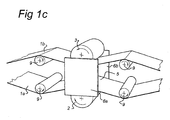
- Both electrodes 2, 3 may have the same configuration being flat orientated (as shown in figure 1a ) or both being roll-electrodes (as shown in figure 1c ).
- different configurations may be applied using a roll electrode and a flat or cylinder segment shaped electrode opposing each other.
- the electrodes may be multi-segment electrodes. Embodiments using more than two electrodes are also imaginable.
- the atmospheric pressure plasma is generated between the two electrodes 2, 3 in the treatment space 5.
- a plurality of electrodes 2, 3 is provided.
- the electrodes 2, 3 have a surface area which is at least as big as the substrate 1, the substrate 1 can be fixed in the treatment space 5 between the two electrodes 2, 3.
- Figure 1b shows a variant wherein two substrates 1a, 1b are treated simultaneously.
- two substrates (1a, 1b) are positioned in a fixed way or moving at a certain speed in the treatment space 5 to utilise the gas supply even more efficiently.
- figure 1c a further example of such an embodiment comprising two side tabs 6a, 6b and two substrates 1a, 1b is shown.
- Both electrodes 2, 3 can be provided with a dielectric barrier layer 2a, 3a (see figure 1b ).
- the dielectric layer 2a on the first electrode 2 has a thickness of d1 (mm)
- the dielectric layer 3a on the second electrode 3 has a thickness of d2 (mm).
- the total dielectric distance d of the electrode configuration also includes the thickness of the (one or two) substrates 1a, 1b to be treated, indicated by f1 (mm) and f2 (mm).
- both d1 and d2 are 0 and the only dielectric material forming the dielectric barrier is the substrate 1a, 1b.
- both d1 and d2 are 0 and only one substrate 1 is used.
- the gap distance g in figure 1c indicates the smallest gap between the electrodes 2, 3 where an atmospheric pressure glow discharge plasma can exist in operation (i.e. in the treatment space 5), also called the free inter-electrode space.
- the dimensions of the electrodes 2, 3, dielectric barrier layers 2a, 3a, and gap g between the electrodes 2, 3, are predetermined in order to generate and sustain a glow discharge plasma at atmospheric pressure in the treatment space 5.
- the dimensions of the electrodes 2, 3, dielectric barrier layers 2a, 3a, and gap g between the electrodes 2, 3 and the total dielectric distance (d) which is the total dielectric thickness of the dielectric barrier are controlled in a further embodiment, such that the product of gap distance and the total dielectric distance is arranged to be less than or equal to 1.0 mm 2 or even more preferred less than 0.5 mm 2 as disclosed in WO 2009/104 957 by applicant.
- the substrate 1 may be moved through the treatment space 5, e. g. at a linear speed using a roll-to-roll configuration, an example of which is shown in the embodiment of figure 1c .
- the substrates 1a, 1b are guided in close contact with the roller shaped (roll) electrodes 2, 3, using guiding rollers 9.
- a roll-electrode is e.g. implemented as a cylinder shaped electrode, mounted to allow rotation in operation e.g. using a mounting shaft or bearings. Such a roll-electrode may be freely rotating, or may be driven at a certain angular speed, e.g. using well known controller and drive units.
- the side tabs 6a, 6b are positioned at the roller end faces, thereby creating a closed off treatment space 5 between the electrodes 2, 3.
- the electrodes 2, 3 are connected to a power supply 4, which is arranged to provide electrical power to the electrodes for generating the atmospheric (glow discharge) plasma.
- a gas supply device 8 may be arranged for the substrate treatment in order to direct the gas for the nitridation step towards an inner region of the substrate to be processed.
- the supply device 8 also acts as the main carrier gas supply.
- a carrier gas may be used such as Argon, Helium, etc., to form the plasma, as an additive or mixture to reduce the breakdown voltage.
- a gas supply inlet 8a may be used to direct the gas into the treatment space 5 as shown in EP 2 226 832 by applicant.
- the gas supply device 8 may be provided with storage, supply and mixing components as known to the skilled person.
- the gas directed to the treatment space for the nitration step is essentially consisting of N 2 (nitrogen) or NH 3 (ammonia) or NO or combination thereof.
- the gas composition may consist besides the presence of N 2 (nitrogen) or NH 3 (ammonia) or NO or combination thereof a small amount of H 2 .
- the total amount of gas supplied to the substrate for the nitridation step is in the range of 1 to 30 slm.
- the temperature in the treatment space 5 during the nitridation step is preferably below 150°C and even preferably below 100°C ; the time of plasma treatment is preferably below the 10 minutes, preferably below 5 and even more preferably below 2 minutes. Excellent results have been found using at most 60 seconds of plasma treatment. As a result excellent barriers can be prepared at very mild conditions i.e. at atmospheric pressure at low temperature and high speed giving high economical value.
- a substrate After the nitridation a substrate remains having a thin inorganic oxide film having a low N-atom concentration amount between 2 and 3%.
- the nitrogen concentration is determined by X-ray Photoelectron Spectroscopy (XPS), using Amicon Electron Spectroscopy for Chemical Analysis (ESCA) equipment manufactured by Kratos.
- XPS X-ray Photoelectron Spectroscopy
- ESCA Amicon Electron Spectroscopy for Chemical Analysis
- Water vapour transmission rate (WVTR) of a typical 50 nm inorganic silicon oxide layer on a PEN 100 ⁇ m sheet film may change remarkably going from about 2 to about 0.002 g/m 2 *day and typical barrier improvement factors after the plasma treatment is 400, 500 or 1000, which is an unforeseen and surprising effect.
- Barrier properties for such thin layers of comparable quality have previously only been reported for thin layers (about 50 nm) prepared by ALD (Atomic Layer Deposition) in a plasma process which is much less efficient and takes much more time as each atomic layer formed in an ALD cycle comprises 4 different steps.
- WVTR is determined using a Mocon Aquatran Model 1 which uses a coloumetric cell (electrochemical cell) with a minimum detection limit of 5*10 -4 g/m 2 *day. This method provides a more sensitive and accurate permeability evaluation than the permeation measurement by using IR absorption. All measurements were done at 40°C/90%RH.
- the free pore volume of the inorganic oxides was determined using the Lorentz-Lorenz equations by measuring the optical density difference of the material. Optical density difference was measured using a Woollam Spectroscopic Ellipsometer equipped with an vacuum chamber and heating stage.
- Typical WVTR of the PET samples after deposition is 5 g/m2*day and for PEN the WVTR is 2 g/m2*day. These WVTR values are similar to the values of the bare polymer film.
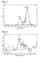
- Figure 2 shows N 1s signal of example 1 before and after the APGD nitridation step (post-treatment).
- FIG. 1 shows the ESCA (XPS) result of the top surface of the corona N 2 treatment.
- LF Low frequency
- DBD dielectric barrier discharge
- Table 2 shows the WVTR (in g/m 2 *day) and barrier improvement factor (BIF) results for the 12 examples treated under the APGD or the corona treatment as nitidation step.
- the nitrogen atom concentration was determined on the examples after the APGD post-treatment.
Landscapes
- Chemical & Material Sciences (AREA)
- Engineering & Computer Science (AREA)
- General Chemical & Material Sciences (AREA)
- Chemical Kinetics & Catalysis (AREA)
- Materials Engineering (AREA)
- Mechanical Engineering (AREA)
- Metallurgy (AREA)
- Organic Chemistry (AREA)
- Inorganic Chemistry (AREA)
- Physics & Mathematics (AREA)
- Plasma & Fusion (AREA)
- Analytical Chemistry (AREA)
- Chemical Vapour Deposition (AREA)
- Laminated Bodies (AREA)
- Application Of Or Painting With Fluid Materials (AREA)
- Electroluminescent Light Sources (AREA)
Description
- The invention relates to a method for manufacturing a barrier layer on a substrate. The present invention further relates to a device for manufacturing such a barrier layer. In addition the invention relates to a substrate having an inorganic oxide barrier layer.
- Nitridation techniques using a nitrogen plasma have been widely studied for application to integrated electronics devices such as gate insulators of metal oxide semiconductor field effect transistors.
- For example
US 7 619 356 describes an anode for an OLED device wherein the anode comprises an Indium Tin Oxide (ITO) film on a glass substrate and the ITO surface is being treated in a plasma treatment at low pressure (14 mTorr) at 50 W power for 5 minutes. As a result of this treatment 13.3% nitrogen atoms are observed from the surface, which amount corresponds to about 275 oxygen atoms. -
US 7 132 373 discloses a method for producing a crystalline metal oxide film (for example a film containing ITO) using a nitrogen or oxygen plasma at a low pressure (50-100 Pa) for at least 3 minutes. -
US 7 898 082 discloses a semiconductor device having a barrier metal nitride layer, the layer formed using a nitrogen plasma at high temperatures of 350-750 degrees Celsius. - Furthermore, Nakae et al describes in the Journal of Applied Physics 101, 023513 (2007) the grow models of silicon nitride ultrathin films fabricated using atmospheric pressure plasma on Si-wafers. In case of nitridation with an RF plasma this was done at a low gas pressure of 1.0 * 10-5 Torr.
-
JP 4 249 520 - In many manufacturing processes involving glass substrates, such as the process of manufacturing OLED devices, there is a desire to replace glass substrates with low weight, flexible polymeric substrates using polymers with a very thin amorphous layer of metal oxide with improved barrier properties.
- Peng et al, J.Electrochem.Soc. vol.154(4), pages G85-G94 shows a method of sealing pores in a porous low dielectric constant film by means of treatment with an ammonia plasma.
- It is an object of the invention to provide a method for creating an improved barrier on a substrate, in particular a flexible substrate.
- According to a present invention embodiment, a method is provided for manufacturing a barrier layer on a substrate, the method comprising:
- providing a substrate with an inorganic oxide layer having a pore volume between 0.3 and 10 vol. % ;
- treating said substrate with an inorganic oxide layer in a glow discharge plasma, said plasma being generated by at least two electrodes in a treatment space formed between said two electrodes, said treatment space also being provided with a gas comprising Nitrogen compounds; and
- the treating of the substrate in said treatment space is done at a temperature below 150°C, e.g. below 100°C.
- In an embodiment, the treatment is done until a barrier with a top layer comprising between 1 to 3% Nitrogen-atom concentration is formed on the substrate.
- In an embodiment the generated plasma is a high frequency or radio frequency (RF) plasma or discharge.
- In an embodiment, the gas comprising Nitrogen compounds comprises N2 (nitrogen) and/or NH3 (ammonia) and/or NO.
- In an embodiment, the gas comprising Nitrogen compounds has a pressure between 0.1 and 10 atmosphere, e.g. between 0.5 and 5 atmosphere (between 5x10⁴ Pa and 5x10⁵ Pa), e.g. between 0.6 and 2 atmosphere (between 6x10⁴ Pa and 2x10⁵ Pa), e.g. substantially 1 atmosphere. At these pressures, typically higher than used in the prior art, the barrier is advantageously formed in less time.
- In an embodiment, the treating of the substrate in said treatment space is done for a duration of less than 20 minutes, e.g. less than 10 minutes. Given the conditions outlined above, this is enough time to form a suitable barrier layer, in particular a barrier having a top layer with 1 to 3% Nitrogen atom concentration.
- In an embodiment, the substrate is a flexible substrate, in particular a flexible polymeric substrate. In a further embodiment, the electrodes are roll-electrodes, and the flexible layer is moved through the treatment space at a linear speed.
- In an embodiment, the inorganic oxide layer of the provided substrate is an silicon-oxide layer.
- In an embodiment, the top layer of the barrier that is formed is between 5 and 15 nm, e.g. between 7 and 12 nm, thick.
- The current disclosure further provides a device for manufacturing a barrier layer on a substrate, the device comprising:
- at least two electrodes, arranged to generate a glow discharge plasma in a treatment space formed between said two electrodes;
- a gas supply device, arranged to provide a gas comprising Nitrogen compounds to the treatment space;
- wherein the treatment space if further arranged to hold and treat at least one substrate having an inorganic oxide layer, and the device is arranged for treating of the substrate in said treatment space at a temperature below 150°C, e.g. below 100°C. The device can further have any of the previously mentioned features of embodiments of the invention.
- The invention further provides a substrate having a barrier layer, the barrier layer comprising an inorganic oxide layer originally, that is, prior to a nitridation step, having a pore size between 0.3 and 10 vol. %, the inorganic oxide layer further having a top layer comprising between 1 to 3% Nitrogen-atom concentration. The substrate and/or the barrier layer may further have any of the abovementioned substrate and/or barrier layer features.
- The method described in this invention gives a remarkable improvement, which is not known from the prior art, using a nitridation step at atmospheric pressure and relatively low temperatures resulting in a product having a small amount concentration N-atoms built-in in the metal oxide surface. The method and device according the invention thus allows the manufacturing of an excellent barrier film, wherein said film may essentially consist of a flexible substrate having a thin inorganic oxide layer having a pore volume from e.g. 0.1 to 20 volume %, e.g. 0.3 to 10 volume %. The method can yield a sealed inorganic oxide layer having between 1 and 3% nitrogen atom concentration in the first 10 nm top layer of the inorganic film. The method comprises at least a treatment step wherein said substrate with the inorganic oxide layer is treated in a plasma, such as an atmospheric plasma, more in particular an atmospheric pressure glow discharge plasma that is generated in a treatment space formed between at least two electrodes, by applying an electrical power from a power supply to the at least two electrodes, resulting in the treatment space in a high frequency electromagnetic field. Said treatment step e.g. lasts for less than 10 minutes at a temperature below 150°C, during which the treatment space being filled with a gas composition comprising a nitrogen compound such as N2 (nitrogen) or NH3 (ammonia) or NO or a combination thereof.
- In another embodiment besides the above mentioned Nitrogen-based molecules, the gas composition may in addition contain a small amount of H2 (hydrogen) gas, which may influence the plasma and barrier properties advantageously.
- As a result of the treatment the inorganic oxide layer becomes sealed and gains a barrier improvement of a factor 1000, which was an unforeseen and surprising effect.
- The method is preferably practiced on a flexible substrate with an inorganic oxide layer having a pore size of 0.1 to 20 volume %, e.g. 0.3 to 10 volume %. A variety of methods are possible for the provision of said substrate, which may be a sputtering method, an ion plating method, and a vacuum evaporation method. Alternatively, the inorganic oxide film can be formed by application of a precursor solution, that is, a wet deposition. In the latter case, the above-mentioned inorganic oxide layer may also be pretreated by ultraviolet light irradiation prior to exposing to plasma.
- The inorganic oxide film substantially is, for example, a thin layer containing a silicon oxide, titanium oxide, aluminum oxide, film containing ITO and the like. The inorganic oxide film thickness may vary between 10 and 1000 nm. Examplary ranges may be between 15 and 100 nm.
- In an embodiment the inorganic oxide film is prepared by exposing a flexible polymeric substrate to an atmospheric plasma deposition apparatus using a precursor as disclosed in
EP 1 917 842 - Preferred precursors which may be used for forming an inorganic oxide layer on a flexible substrate by using an atmospheric plasma as described in
WO 2009 104 957 are TEOS, HMDSO, TPOT, TEOT, TMA, TEA. - The flexible substrate may be any kind of polymeric film. In an exemplary embodiment PET or PEN film is used having a thickness of 50 to 200 µm.
- Other examples of substrate which may be used are transparent sheets of ethylene vinyl acetate (EVA), of polyvinyl butyral (PVB), of polytetrafluoroethylene (PTFE), perfluoroalcoxy resins (PFA), i.e., copolymers of tetrafluoroethylene and perfluoroalkyl vinyl ether, tetafluoroethylene-hexafluoropropylene copolymers (FEP), tetrafluoroethylene-perfluoroalkyl vinyl ether-hexafluoro-propylene copolymers (EPE), tetrafluoroethylene-ethylene or propylenecopolymers (ETFE), polychlorotrifluoroethylene resins (PCTFE), ethylene-chlorotrifluoroethylene copolymers (ECTFE), vinylidene fluoride resins (PVDF), and polyvinyl fluorides (PVF) or coextruded sheets from polyester with EVA, polycarbonate, polyolefin, polyurethane, liquid crystal polymer, aclar, aluminum, of sputtered aluminum oxide polyester, sputtered silicon oxide or silicon nitride polyester, sputtered aluminum oxide polycarbonate, and sputtered silicon oxide or silicon nitride polycarbonate.
- The present invention will be discussed in more detail below, using a number of exemplary embodiments, with reference to the attached drawings, in which
-
Figures 1a, 1b , and1c show schematic views of a plasma generation device used in the invention. -
Figure 2 shows the Electron Spectroscopy for Chemical Analysis (ESCA) or X-ray Photoelectron Spectroscopy (XPS) result of the top surface of an embodiment after an atmospheric pressure glow discharge nitridation treatment. -
Figure 3 shows the ESCA (XPS) result of the top surface of a corona N2 treatment of example 1. - The present invention will now be described in reference to exemplary embodiments of the invention.
-
Figure 1a shows a schematic view of a plasma apparatus with which the present invention may be practiced. Atreatment space 5, which may be a treatment chamber within an enclosure (not shown infigure 1a ), or atreatment space 5 with an open structure, comprises twoelectrodes electrodes dielectric barrier figure 1b ) in order to be able to generate and sustain a glow discharge at atmospheric pressure in the treatment space. In the embodiment shown, theelectrodes treatment space 5 is a rectangular space. Aside tab 6 is provided to close off thetreatment space 5 on one side. - However, other forms of the
electrodes treatment space 5 are possible, e.g. as part of a cylindrical arrangement of the plasma treatment apparatus. E.g., the treatment space may be cylindrical, or elliptic, or have another form adapted to treat a specific type ofsubstrate 1. Bothelectrodes figure 1a ) or both being roll-electrodes (as shown infigure 1c ). Also different configurations may be applied using a roll electrode and a flat or cylinder segment shaped electrode opposing each other. In further embodiments, the electrodes may be multi-segment electrodes. Embodiments using more than two electrodes are also imaginable. - In general the atmospheric pressure plasma is generated between the two
electrodes treatment space 5. Alternatively a plurality ofelectrodes electrodes substrate 1, thesubstrate 1 can be fixed in thetreatment space 5 between the twoelectrodes -
Figure 1b shows a variant wherein twosubstrates substrate 1 but two substrates (1a, 1b) are positioned in a fixed way or moving at a certain speed in thetreatment space 5 to utilise the gas supply even more efficiently. Infigure 1c a further example of such an embodiment comprising twoside tabs substrates - Both
electrodes dielectric barrier layer figure 1b ). Thedielectric layer 2a on thefirst electrode 2 has a thickness of d1 (mm), and thedielectric layer 3a on thesecond electrode 3 has a thickness of d2 (mm). In operation, the total dielectric distance d of the electrode configuration also includes the thickness of the (one or two)substrates treatment space 5 between the at least two opposing electrodes (2, 3) equals d = d1+f1+f2+d2. - In a further embodiment, both d1 and d2 are 0 and the only dielectric material forming the dielectric barrier is the
substrate substrates - In still another embodiment both d1 and d2 are 0 and only one
substrate 1 is used. In this embodiment the total dielectric thickness equals f1, so d = f1. Also in this embodiment in whichelectrode 3 is not covered with a dielectric material it is possible to obtain a stable atmospheric glow discharge plasma. The gap distance g infigure 1c indicates the smallest gap between theelectrodes electrodes dielectric barrier layers electrodes treatment space 5. - The dimensions of the
electrodes dielectric barrier layers electrodes WO 2009/104 957 by applicant. - In case the
substrate 1 is larger than the electrode area, thesubstrate 1 may be moved through thetreatment space 5, e. g. at a linear speed using a roll-to-roll configuration, an example of which is shown in the embodiment offigure 1c . Thesubstrates electrodes side tabs treatment space 5 between theelectrodes - The
electrodes - The power supply can be a power supply providing a wide range of frequencies for example f = 10 kHz - 30MHz.
- Very good results can be obtained by using an atmospheric pressure glow discharge (APGD) plasma. Until recently these plasma's suffered from a bad stability, but using the stabilization circuits as for example described in
US 6 774 569EP 1 383 359EP 1 547 123EP 1 626 613figure 1a ) counteracting local instabilities in the plasma. Using thestabilization circuit 21 in combination with theAC power source 20 in the power supply 4 for the plasma generating apparatus results in a controlled and stable plasma, without streamers, filamentary discharges or other imperfections. - In the plasma treatment apparatus a
gas supply device 8 may be arranged for the substrate treatment in order to direct the gas for the nitridation step towards an inner region of the substrate to be processed. Thesupply device 8 also acts as the main carrier gas supply. A carrier gas may be used such as Argon, Helium, etc., to form the plasma, as an additive or mixture to reduce the breakdown voltage. - A
gas supply inlet 8a may be used to direct the gas into thetreatment space 5 as shown inEP 2 226 832gas supply device 8 may be provided with storage, supply and mixing components as known to the skilled person. - The gas directed to the treatment space for the nitration step is essentially consisting of N2 (nitrogen) or NH3 (ammonia) or NO or combination thereof. In further embodiments the gas composition may consist besides the presence of N2 (nitrogen) or NH3 (ammonia) or NO or combination thereof a small amount of H2.
- The total amount of gas supplied to the substrate for the nitridation step is in the range of 1 to 30 slm.
- Further the temperature in the
treatment space 5 during the nitridation step is preferably below 150°C and even preferably below 100°C ; the time of plasma treatment is preferably below the 10 minutes, preferably below 5 and even more preferably below 2 minutes. Excellent results have been found using at most 60 seconds of plasma treatment. As a result excellent barriers can be prepared at very mild conditions i.e. at atmospheric pressure at low temperature and high speed giving high economical value. - After the nitridation a substrate remains having a thin inorganic oxide film having a low N-atom concentration amount between 2 and 3%.
- The nitrogen concentration is determined by X-ray Photoelectron Spectroscopy (XPS), using Amicon Electron Spectroscopy for Chemical Analysis (ESCA) equipment manufactured by Kratos.
- Water vapour transmission rate (WVTR) of a typical 50 nm inorganic silicon oxide layer on a PEN 100 µm sheet film may change remarkably going from about 2 to about 0.002 g/m2*day and typical barrier improvement factors after the plasma treatment is 400, 500 or 1000, which is an unforeseen and surprising effect. Barrier properties for such thin layers of comparable quality have previously only been reported for thin layers (about 50 nm) prepared by ALD (Atomic Layer Deposition) in a plasma process which is much less efficient and takes much more time as each atomic layer formed in an ALD cycle comprises 4 different steps.
- WVTR is determined using a
Mocon Aquatran Model 1 which uses a coloumetric cell (electrochemical cell) with a minimum detection limit of 5*10-4 g/m2*day. This method provides a more sensitive and accurate permeability evaluation than the permeation measurement by using IR absorption. All measurements were done at 40°C/90%RH. - The free pore volume of the inorganic oxides was determined using the Lorentz-Lorenz equations by measuring the optical density difference of the material. Optical density difference was measured using a Woollam Spectroscopic Ellipsometer equipped with an vacuum chamber and heating stage.
- Several samples (rolls) were prepared by depositing PEN (100 µm thick) or PET (100 µm thick) using an atmospheric pressure glow discharge plasma apparatus as disclosed in
WO 2009 104 957 in a treatment space using a plasma power of 600 W, an excitation energy of 200 kHz and a gas composition (95% N2/5% O2) using different precursors (HMDSO/TEOS) resulting in the following 12 examples all having 50 nm inorganic oxide (Silicon oxide) layer.Table 1 Substrate Precursor Pore (vol. %) Example 1-4 PEN HMDSO 0.4∼3 Example 5-8 PET HMDSO 0.3∼2 Example 9-12 PET TEOS 0.3∼3 - Typical WVTR of the PET samples after deposition is 5 g/m2*day and for PEN the WVTR is 2 g/m2*day. These WVTR values are similar to the values of the bare polymer film.
- As next step a part of the 12 examples were treated using the same atmospheric pressure plasma apparatus (APGD) as described in
WO 2009 104 957 using a plasma power of 300 W, an excitation energy of 200 kHz however as gas composition of 1) 100% N2 (10 slm) or 2) 95% N2+5%NH3 (10 slm) or 3) 98% N2+2%NO (10 slm) or 4) 90% N2+10%H2 (10 slm). The nitridation step was done in 60 seconds at a temperature of 90 °C. -
Figure 2 shows N 1s signal of example 1 before and after the APGD nitridation step (post-treatment). - Another part of the same 12 examples were treated using a Low frequency (LF) dielectric barrier discharge (DBD) corona plasma using Softal corona unit type VTG 3005 (corona discharge treatment) equipment under the same gas compositions 1 - 4 described as above.
Figure 3 shows the ESCA (XPS) result of the top surface of the corona N2 treatment. - Table 2 shows the WVTR (in g/m2*day) and barrier improvement factor (BIF) results for the 12 examples treated under the APGD or the corona treatment as nitidation step. The nitrogen atom concentration was determined on the examples after the APGD post-treatment.
- Although in all cases an improvement of the barrier performance is observed the best results are obtained (even with a barrier improvement factor of about 1000) by using a high frequency APG discharge for the nitridation step.
Table 2 Gas APGD WVTR@ (g/m2*day) APGD BIF APGD N%(*) Corona WVTR Corona BIF Example 1 N2 0.003 666 1.3 1.0 2 Example 2 N2/NH3 <0.002 >1000 2.9 0.5 4 Example 3 N2/NO 0.005 400 1.1 1.2 2 Example 4 N2/H2 0.003 666 1.6 0.8 2.5 Example 5 N2 <0.002 >2500 2.2 3 1.7 Example 6 N2/NH3 <0.002 >2500 2.7 1.6 3 Example 7 N2/NO 0.005 1000 1.8 3.9 1.3 Example 8 N2/H2 <0.002 >2500 2.1 2.0 2.5 Example 9 N2 <0.002 >2500 2.5 3.1 1.6 Example 10 N2/NH3 <0.002 >2500 2.8 2.0 2.5 Example 11 N2/NO 0.006 833 1.4 3.5 1.4 Example 12 N2/H2 <0.002 >2500 0.9 2.1 2.4 (*): XPS reveals that as a result of the nitridation step a distinct low energy N1s peak appears which is attributed to N-Si3 bonding.
(@): background signal has not been subtracted; as back ground signal is in the order of about 0.002 the WVTR of examples 2, 5, 6, 8, 9, 10, 12 are in fact lower than 0.002 which as been denoted as <0.002.
Claims (13)
- A method for manufacturing a barrier layer on a substrate (1, 1a, 1b), the method comprising:- providing a substrate (1, 1a, 1b) with an inorganic oxide layer having a pore volume between 0.3 and 10 vol. %;- treating said substrate with an inorganic oxide layer in a glow discharge plasma, said plasma being generated by at least two electrodes (2, 3) in a treatment space (5) formed between said two electrodes, said treatment space also being provided with a gas comprising Nitrogen compounds; and- the treating of the substrate in said treatment space is done at a temperature below 150°C, e.g. below 100°C.
- Method according to claim 1, wherein the treatment of the substrate is done until a barrier with a top layer comprising between 1 to 3% Nitrogen-atom concentration is formed.
- Method according to claim 1 or 2, wherein the gas comprising Nitrogen compounds, comprises N2 (nitrogen) and/or NH3 (ammonia) and/or NO.
- Method according to any of the preceding claims, wherein the gas comprising Nitrogen compounds has a pressure between 0.1 and 10 atmosphere, e.g. between 0.5 and 5 atmosphere, e.g. between 0.6 and 2 atmosphere or approximately 1 atmosphere.
- Method according to any of the preceding claims, wherein the treating of the substrate (1, 1a, 1b) in said treatment space is done for a duration of less than 10 minutes, e.g. less than 5 minutes, e.g. less than 2 minutes, e.g. a duration of 60 seconds.
- Method according to any of the preceding claims, wherein the substrate (1, 1a, 1b) is a flexible substrate, in particular a flexible polymeric substrate.
- Method according to claim 6, wherein the electrodes (2, 3) are roll-electrodes, and the flexible layer is moved through the treatment space (5) at a linear speed.
- Method according to any of the preceding claims, wherein the inorganic oxide layer of the provided substrate (1, 1a, 1) is a silicon-oxide layer.
- Method according to any of the preceding claims, wherein the top layer is between 5 and 15 nm, e.g. between 7 and 12 nm, thick.
- Substrate (1, 1a, 1b) having a barrier layer, the barrier layer comprising an inorganic oxide layer having a pore volume between 0.3 and 10 vol. %, the inorganic oxide layer further having a top layer comprising between 1 to 3% Nitrogen-atom concentration.
- Substrate (1, 1a, 1b) according to claim 10, wherein the inorganic oxide layer of the provided substrate is a silicon-oxide layer.
- Substrate (1, 1a, 1b) according to claim 10 or 11, wherein the substrate (1, 1a, 1b) is a flexible substrate, in particular a flexible polymeric substrate.
- Substrate (1, 1a, 1b) according to any of the claims 10-12, wherein the top layer is between 5 and 15 nm, e.g. between 7 and 12 nm, thick
Applications Claiming Priority (2)
| Application Number | Priority Date | Filing Date | Title |
|---|---|---|---|
| GBGB1110117.7A GB201110117D0 (en) | 2011-06-16 | 2011-06-16 | method and device for manufacturing a barrie layer on a flexible substrate |
| PCT/GB2012/050897 WO2012172304A1 (en) | 2011-06-16 | 2012-04-24 | Method and device for manufacturing a barrier layer on a flexible substrate |
Publications (2)
| Publication Number | Publication Date |
|---|---|
| EP2721193A1 EP2721193A1 (en) | 2014-04-23 |
| EP2721193B1 true EP2721193B1 (en) | 2015-03-04 |
Family
ID=44357840
Family Applications (1)
| Application Number | Title | Priority Date | Filing Date |
|---|---|---|---|
| EP12719037.9A Not-in-force EP2721193B1 (en) | 2011-06-16 | 2012-04-24 | Method for manufacturing a barrier layer on a flexible substrate |
Country Status (5)
| Country | Link |
|---|---|
| US (2) | US9117663B2 (en) |
| EP (1) | EP2721193B1 (en) |
| JP (1) | JP2014519558A (en) |
| GB (1) | GB201110117D0 (en) |
| WO (1) | WO2012172304A1 (en) |
Families Citing this family (34)
| Publication number | Priority date | Publication date | Assignee | Title |
|---|---|---|---|---|
| GB201210836D0 (en) * | 2012-06-19 | 2012-08-01 | Fujifilm Mfg Europe Bv | Method and device for manufacturing a barrier layer on a flexible substrate |
| JP6117124B2 (en) * | 2013-03-19 | 2017-04-19 | 富士フイルム株式会社 | Oxide semiconductor film and manufacturing method thereof |
| GB201403551D0 (en) | 2014-02-28 | 2014-04-16 | Fujifilm Mfg Europe Bv | Membrane stacks |
| CN106783720B (en) * | 2017-03-03 | 2020-06-23 | 京东方科技集团股份有限公司 | A display substrate and method of making the same |
| US10224224B2 (en) | 2017-03-10 | 2019-03-05 | Micromaterials, LLC | High pressure wafer processing systems and related methods |
| US10847360B2 (en) * | 2017-05-25 | 2020-11-24 | Applied Materials, Inc. | High pressure treatment of silicon nitride film |
| US10622214B2 (en) | 2017-05-25 | 2020-04-14 | Applied Materials, Inc. | Tungsten defluorination by high pressure treatment |
| CN110678973B (en) | 2017-06-02 | 2023-09-19 | 应用材料公司 | Dry stripping of boron carbide hard masks |
| US10234630B2 (en) | 2017-07-12 | 2019-03-19 | Applied Materials, Inc. | Method for creating a high refractive index wave guide |
| US10269571B2 (en) | 2017-07-12 | 2019-04-23 | Applied Materials, Inc. | Methods for fabricating nanowire for semiconductor applications |
| US10179941B1 (en) | 2017-07-14 | 2019-01-15 | Applied Materials, Inc. | Gas delivery system for high pressure processing chamber |
| KR102405723B1 (en) | 2017-08-18 | 2022-06-07 | 어플라이드 머티어리얼스, 인코포레이티드 | High pressure and high temperature annealing chamber |
| US10276411B2 (en) | 2017-08-18 | 2019-04-30 | Applied Materials, Inc. | High pressure and high temperature anneal chamber |
| WO2019055415A1 (en) | 2017-09-12 | 2019-03-21 | Applied Materials, Inc. | Apparatus and methods for manufacturing semiconductor structures using protective barrier layer |
| US10643867B2 (en) | 2017-11-03 | 2020-05-05 | Applied Materials, Inc. | Annealing system and method |
| EP3707746B1 (en) | 2017-11-11 | 2023-12-27 | Micromaterials LLC | Gas delivery system for high pressure processing chamber |
| WO2019099125A1 (en) | 2017-11-16 | 2019-05-23 | Applied Materials, Inc. | High pressure steam anneal processing apparatus |
| JP2021503714A (en) | 2017-11-17 | 2021-02-12 | アプライド マテリアルズ インコーポレイテッドApplied Materials,Incorporated | Capacitor system for high pressure processing system |
| JP7299898B2 (en) | 2018-01-24 | 2023-06-28 | アプライド マテリアルズ インコーポレイテッド | Seam repair using high pressure annealing |
| KR102702244B1 (en) | 2018-03-09 | 2024-09-03 | 어플라이드 머티어리얼스, 인코포레이티드 | High pressure annealing process for metal containing materials |
| US10714331B2 (en) | 2018-04-04 | 2020-07-14 | Applied Materials, Inc. | Method to fabricate thermally stable low K-FinFET spacer |
| US10950429B2 (en) | 2018-05-08 | 2021-03-16 | Applied Materials, Inc. | Methods of forming amorphous carbon hard mask layers and hard mask layers formed therefrom |
| US10566188B2 (en) | 2018-05-17 | 2020-02-18 | Applied Materials, Inc. | Method to improve film stability |
| US10704141B2 (en) | 2018-06-01 | 2020-07-07 | Applied Materials, Inc. | In-situ CVD and ALD coating of chamber to control metal contamination |
| US10748783B2 (en) | 2018-07-25 | 2020-08-18 | Applied Materials, Inc. | Gas delivery module |
| US10675581B2 (en) | 2018-08-06 | 2020-06-09 | Applied Materials, Inc. | Gas abatement apparatus |
| JP7179172B6 (en) | 2018-10-30 | 2022-12-16 | アプライド マテリアルズ インコーポレイテッド | Method for etching structures for semiconductor applications |
| CN112996950B (en) | 2018-11-16 | 2024-04-05 | 应用材料公司 | Film deposition using enhanced diffusion process |
| WO2020117462A1 (en) | 2018-12-07 | 2020-06-11 | Applied Materials, Inc. | Semiconductor processing system |
| US11996540B2 (en) | 2019-12-20 | 2024-05-28 | Intecells, Inc. | Method and apparatus for making lithium ion battery electrodes |
| US11621411B2 (en) * | 2019-12-23 | 2023-04-04 | Intecells, Inc. | Method of insulating lithium ion electrochemical cell components with metal oxide coatings |
| US11901222B2 (en) | 2020-02-17 | 2024-02-13 | Applied Materials, Inc. | Multi-step process for flowable gap-fill film |
| GB202109309D0 (en) * | 2021-06-29 | 2021-08-11 | Fujifilm Mfg Europe Bv | Gas separation membranes |
| SE2330191A1 (en) | 2023-05-01 | 2024-11-02 | Volvo Truck Corp | Radar-based wheel end modules for determining wheel force generating capability |
Family Cites Families (29)
| Publication number | Priority date | Publication date | Assignee | Title |
|---|---|---|---|---|
| JPH04249520A (en) | 1991-01-08 | 1992-09-04 | Matsushita Electric Works Ltd | Liquid epoxy resin molding material |
| US6913796B2 (en) * | 2000-03-20 | 2005-07-05 | Axcelis Technologies, Inc. | Plasma curing process for porous low-k materials |
| US6794311B2 (en) * | 2000-07-14 | 2004-09-21 | Applied Materials Inc. | Method and apparatus for treating low k dielectric layers to reduce diffusion |
| JP2003068850A (en) * | 2001-08-29 | 2003-03-07 | Tokyo Electron Ltd | Semiconductor device and method of manufacturing the same |
| US7132373B2 (en) | 2001-10-02 | 2006-11-07 | Toto Ltd. | Thin metal oxide film and process for producing the same |
| JP2003264058A (en) * | 2002-03-07 | 2003-09-19 | Konica Corp | Substrate, and organic electroluminescent display using this substrate |
| US6774569B2 (en) | 2002-07-11 | 2004-08-10 | Fuji Photo Film B.V. | Apparatus for producing and sustaining a glow discharge plasma under atmospheric conditions |
| US7288204B2 (en) | 2002-07-19 | 2007-10-30 | Fuji Photo Film B.V. | Method and arrangement for treating a substrate with an atmospheric pressure glow plasma (APG) |
| US20050202168A1 (en) * | 2002-08-16 | 2005-09-15 | General Electric Company | Thermally-stabilized thermal barrier coating and process therefor |
| EP1403902A1 (en) * | 2002-09-30 | 2004-03-31 | Fuji Photo Film B.V. | Method and arrangement for generating an atmospheric pressure glow discharge plasma (APG) |
| JP4249520B2 (en) * | 2003-03-19 | 2009-04-02 | 大日本印刷株式会社 | Method for producing gas barrier laminate |
| KR100808790B1 (en) | 2003-05-23 | 2008-03-03 | 주식회사 엘지화학 | ITO film treated with nitrogen plasma and organic light emitting device using the same as anode |
| JP4057972B2 (en) * | 2003-07-25 | 2008-03-05 | 富士通株式会社 | Manufacturing method of semiconductor device |
| JP2005142325A (en) * | 2003-11-06 | 2005-06-02 | Semiconductor Leading Edge Technologies Inc | Semiconductor device and manufacturing method thereof |
| EP1548795A1 (en) | 2003-12-22 | 2005-06-29 | Fuji Photo Film B.V. | Method and apparatus for stabilizing a glow discharge plasma under atmospheric conditions |
| EP1697962B1 (en) | 2003-12-22 | 2009-12-09 | FUJIFILM Manufacturing Europe B.V. | Method of and arrangement for removing contaminants from a substrate surface using an atmospheric pressure glow plasma |
| ATE348497T1 (en) | 2004-08-13 | 2007-01-15 | Fuji Photo Film Bv | METHOD AND DEVICE FOR CONTROLLING A GLOW DISCHARGE PLASMA UNDER ATMOSPHERIC PRESSURE |
| TWI251277B (en) * | 2004-12-31 | 2006-03-11 | Ind Tech Res Inst | Method for forming a silicon oxide layer |
| US7229918B2 (en) | 2005-02-14 | 2007-06-12 | Infineon Technologies Ag | Nitrogen rich barrier layers and methods of fabrication thereof |
| JP4698310B2 (en) * | 2005-07-11 | 2011-06-08 | 富士フイルム株式会社 | Gas barrier film, substrate film and organic electroluminescence device |
| EP1917842B1 (en) | 2005-08-26 | 2015-03-11 | FUJIFILM Manufacturing Europe B.V. | Method and arrangement for generating and controlling a discharge plasma |
| US20080242118A1 (en) * | 2007-03-29 | 2008-10-02 | International Business Machines Corporation | Methods for forming dense dielectric layer over porous dielectrics |
| EP2243859A4 (en) * | 2008-02-19 | 2013-09-25 | Konica Minolta Holdings Inc | Thin film forming method and thin film stack |
| EP2528082A3 (en) | 2008-02-21 | 2014-11-05 | FUJIFILM Manufacturing Europe B.V. | Plasma treatment apparatus with an atmospheric pressure glow discharge electrode configuration |
| US7629264B2 (en) * | 2008-04-09 | 2009-12-08 | International Business Machines Corporation | Structure and method for hybrid tungsten copper metal contact |
| KR20090116477A (en) * | 2008-05-07 | 2009-11-11 | 삼성전자주식회사 | Method for manufacturing a semiconductor device comprising an ultra low dielectric film |
| JP5173863B2 (en) * | 2009-01-20 | 2013-04-03 | パナソニック株式会社 | Semiconductor device and manufacturing method thereof |
| EP2226832A1 (en) | 2009-03-06 | 2010-09-08 | FUJIFILM Manufacturing Europe B.V. | Substrate plasma treatment using side tabs |
| US8334202B2 (en) * | 2009-11-03 | 2012-12-18 | Infineon Technologies Ag | Device fabricated using an electroplating process |
-
2011
- 2011-06-16 GB GBGB1110117.7A patent/GB201110117D0/en not_active Ceased
-
2012
- 2012-04-24 JP JP2014515276A patent/JP2014519558A/en active Pending
- 2012-04-24 US US14/126,572 patent/US9117663B2/en active Active
- 2012-04-24 WO PCT/GB2012/050897 patent/WO2012172304A1/en not_active Ceased
- 2012-04-24 EP EP12719037.9A patent/EP2721193B1/en not_active Not-in-force
-
2015
- 2015-07-15 US US14/799,603 patent/US9390908B2/en not_active Expired - Fee Related
Also Published As
| Publication number | Publication date |
|---|---|
| US9117663B2 (en) | 2015-08-25 |
| US20140138802A1 (en) | 2014-05-22 |
| US20150315701A1 (en) | 2015-11-05 |
| EP2721193A1 (en) | 2014-04-23 |
| JP2014519558A (en) | 2014-08-14 |
| US9390908B2 (en) | 2016-07-12 |
| WO2012172304A1 (en) | 2012-12-20 |
| GB201110117D0 (en) | 2011-07-27 |
Similar Documents
| Publication | Publication Date | Title |
|---|---|---|
| US9390908B2 (en) | Method and device for manufacturing a barrier layer on a flexible substrate | |
| EP2764133B1 (en) | A method for producing a coating by atmospheric pressure plasma technology | |
| JP5725865B2 (en) | Plasma processing apparatus and method for processing a substrate using an atmospheric pressure glow discharge electrode configuration | |
| WO2010021326A1 (en) | Moulded article, method for producing the same, electronic device member, and electronic device | |
| JP5747915B2 (en) | Method for producing gas barrier film | |
| EP2363511B1 (en) | Film deposition method and film deposition device | |
| EP2396451B1 (en) | Two layer barrier on polymeric substrate | |
| KR20170069229A (en) | High-speed deposition of mixed oxide barrier films | |
| EP2861778B1 (en) | Method for manufacturing a barrier layer on a flexible substrate | |
| JP5781350B2 (en) | GAS BARRIER LAMINATE, ITS MANUFACTURING METHOD, ELECTRONIC DEVICE MEMBER AND ELECTRONIC DEVICE | |
| CN87104355A (en) | multi-chamber deposition system | |
| CN108349210B (en) | Gas barrier film | |
| KR20190054940A (en) | Gas barrier layer, gas barrier film, organic electroluminescence element and electronic paper, and method for producing of gas barrier film | |
| KR20000055083A (en) | a method of manufacturing thin films used for semiconductor devices |
Legal Events
| Date | Code | Title | Description |
|---|---|---|---|
| PUAI | Public reference made under article 153(3) epc to a published international application that has entered the european phase |
Free format text: ORIGINAL CODE: 0009012 |
|
| 17P | Request for examination filed |
Effective date: 20131204 |
|
| AK | Designated contracting states |
Kind code of ref document: A1 Designated state(s): AL AT BE BG CH CY CZ DE DK EE ES FI FR GB GR HR HU IE IS IT LI LT LU LV MC MK MT NL NO PL PT RO RS SE SI SK SM TR |
|
| DAX | Request for extension of the european patent (deleted) | ||
| GRAP | Despatch of communication of intention to grant a patent |
Free format text: ORIGINAL CODE: EPIDOSNIGR1 |
|
| INTG | Intention to grant announced |
Effective date: 20141015 |
|
| GRAS | Grant fee paid |
Free format text: ORIGINAL CODE: EPIDOSNIGR3 |
|
| GRAA | (expected) grant |
Free format text: ORIGINAL CODE: 0009210 |
|
| AK | Designated contracting states |
Kind code of ref document: B1 Designated state(s): AL AT BE BG CH CY CZ DE DK EE ES FI FR GB GR HR HU IE IS IT LI LT LU LV MC MK MT NL NO PL PT RO RS SE SI SK SM TR |
|
| REG | Reference to a national code |
Ref country code: GB Ref legal event code: FG4D |
|
| REG | Reference to a national code |
Ref country code: CH Ref legal event code: EP |
|
| REG | Reference to a national code |
Ref country code: IE Ref legal event code: FG4D |
|
| REG | Reference to a national code |
Ref country code: AT Ref legal event code: REF Ref document number: 713988 Country of ref document: AT Kind code of ref document: T Effective date: 20150415 |
|
| REG | Reference to a national code |
Ref country code: DE Ref legal event code: R096 Ref document number: 602012005642 Country of ref document: DE Effective date: 20150416 |
|
| REG | Reference to a national code |
Ref country code: NL Ref legal event code: T3 |
|
| REG | Reference to a national code |
Ref country code: AT Ref legal event code: MK05 Ref document number: 713988 Country of ref document: AT Kind code of ref document: T Effective date: 20150304 |
|
| PG25 | Lapsed in a contracting state [announced via postgrant information from national office to epo] |
Ref country code: LT Free format text: LAPSE BECAUSE OF FAILURE TO SUBMIT A TRANSLATION OF THE DESCRIPTION OR TO PAY THE FEE WITHIN THE PRESCRIBED TIME-LIMIT Effective date: 20150304 Ref country code: FI Free format text: LAPSE BECAUSE OF FAILURE TO SUBMIT A TRANSLATION OF THE DESCRIPTION OR TO PAY THE FEE WITHIN THE PRESCRIBED TIME-LIMIT Effective date: 20150304 Ref country code: NO Free format text: LAPSE BECAUSE OF FAILURE TO SUBMIT A TRANSLATION OF THE DESCRIPTION OR TO PAY THE FEE WITHIN THE PRESCRIBED TIME-LIMIT Effective date: 20150604 Ref country code: SE Free format text: LAPSE BECAUSE OF FAILURE TO SUBMIT A TRANSLATION OF THE DESCRIPTION OR TO PAY THE FEE WITHIN THE PRESCRIBED TIME-LIMIT Effective date: 20150304 Ref country code: HR Free format text: LAPSE BECAUSE OF FAILURE TO SUBMIT A TRANSLATION OF THE DESCRIPTION OR TO PAY THE FEE WITHIN THE PRESCRIBED TIME-LIMIT Effective date: 20150304 Ref country code: ES Free format text: LAPSE BECAUSE OF FAILURE TO SUBMIT A TRANSLATION OF THE DESCRIPTION OR TO PAY THE FEE WITHIN THE PRESCRIBED TIME-LIMIT Effective date: 20150304 |
|
| REG | Reference to a national code |
Ref country code: LT Ref legal event code: MG4D |
|
| PG25 | Lapsed in a contracting state [announced via postgrant information from national office to epo] |
Ref country code: RS Free format text: LAPSE BECAUSE OF FAILURE TO SUBMIT A TRANSLATION OF THE DESCRIPTION OR TO PAY THE FEE WITHIN THE PRESCRIBED TIME-LIMIT Effective date: 20150304 Ref country code: LV Free format text: LAPSE BECAUSE OF FAILURE TO SUBMIT A TRANSLATION OF THE DESCRIPTION OR TO PAY THE FEE WITHIN THE PRESCRIBED TIME-LIMIT Effective date: 20150304 Ref country code: AT Free format text: LAPSE BECAUSE OF FAILURE TO SUBMIT A TRANSLATION OF THE DESCRIPTION OR TO PAY THE FEE WITHIN THE PRESCRIBED TIME-LIMIT Effective date: 20150304 Ref country code: GR Free format text: LAPSE BECAUSE OF FAILURE TO SUBMIT A TRANSLATION OF THE DESCRIPTION OR TO PAY THE FEE WITHIN THE PRESCRIBED TIME-LIMIT Effective date: 20150605 |
|
| PG25 | Lapsed in a contracting state [announced via postgrant information from national office to epo] |
Ref country code: RO Free format text: LAPSE BECAUSE OF FAILURE TO SUBMIT A TRANSLATION OF THE DESCRIPTION OR TO PAY THE FEE WITHIN THE PRESCRIBED TIME-LIMIT Effective date: 20150304 Ref country code: PT Free format text: LAPSE BECAUSE OF FAILURE TO SUBMIT A TRANSLATION OF THE DESCRIPTION OR TO PAY THE FEE WITHIN THE PRESCRIBED TIME-LIMIT Effective date: 20150706 Ref country code: EE Free format text: LAPSE BECAUSE OF FAILURE TO SUBMIT A TRANSLATION OF THE DESCRIPTION OR TO PAY THE FEE WITHIN THE PRESCRIBED TIME-LIMIT Effective date: 20150304 Ref country code: CZ Free format text: LAPSE BECAUSE OF FAILURE TO SUBMIT A TRANSLATION OF THE DESCRIPTION OR TO PAY THE FEE WITHIN THE PRESCRIBED TIME-LIMIT Effective date: 20150304 Ref country code: SK Free format text: LAPSE BECAUSE OF FAILURE TO SUBMIT A TRANSLATION OF THE DESCRIPTION OR TO PAY THE FEE WITHIN THE PRESCRIBED TIME-LIMIT Effective date: 20150304 |
|
| PG25 | Lapsed in a contracting state [announced via postgrant information from national office to epo] |
Ref country code: PL Free format text: LAPSE BECAUSE OF FAILURE TO SUBMIT A TRANSLATION OF THE DESCRIPTION OR TO PAY THE FEE WITHIN THE PRESCRIBED TIME-LIMIT Effective date: 20150304 Ref country code: IS Free format text: LAPSE BECAUSE OF FAILURE TO SUBMIT A TRANSLATION OF THE DESCRIPTION OR TO PAY THE FEE WITHIN THE PRESCRIBED TIME-LIMIT Effective date: 20150704 Ref country code: MC Free format text: LAPSE BECAUSE OF FAILURE TO SUBMIT A TRANSLATION OF THE DESCRIPTION OR TO PAY THE FEE WITHIN THE PRESCRIBED TIME-LIMIT Effective date: 20150304 |
|
| REG | Reference to a national code |
Ref country code: CH Ref legal event code: PL |
|
| REG | Reference to a national code |
Ref country code: DE Ref legal event code: R097 Ref document number: 602012005642 Country of ref document: DE |
|
| PG25 | Lapsed in a contracting state [announced via postgrant information from national office to epo] |
Ref country code: IT Free format text: LAPSE BECAUSE OF FAILURE TO SUBMIT A TRANSLATION OF THE DESCRIPTION OR TO PAY THE FEE WITHIN THE PRESCRIBED TIME-LIMIT Effective date: 20150304 |
|
| PLBE | No opposition filed within time limit |
Free format text: ORIGINAL CODE: 0009261 |
|
| STAA | Information on the status of an ep patent application or granted ep patent |
Free format text: STATUS: NO OPPOSITION FILED WITHIN TIME LIMIT |
|
| REG | Reference to a national code |
Ref country code: IE Ref legal event code: MM4A |
|
| PG25 | Lapsed in a contracting state [announced via postgrant information from national office to epo] |
Ref country code: DK Free format text: LAPSE BECAUSE OF FAILURE TO SUBMIT A TRANSLATION OF THE DESCRIPTION OR TO PAY THE FEE WITHIN THE PRESCRIBED TIME-LIMIT Effective date: 20150304 Ref country code: CH Free format text: LAPSE BECAUSE OF NON-PAYMENT OF DUE FEES Effective date: 20150430 Ref country code: LI Free format text: LAPSE BECAUSE OF NON-PAYMENT OF DUE FEES Effective date: 20150430 |
|
| 26N | No opposition filed |
Effective date: 20151207 |
|
| PG25 | Lapsed in a contracting state [announced via postgrant information from national office to epo] |
Ref country code: SI Free format text: LAPSE BECAUSE OF FAILURE TO SUBMIT A TRANSLATION OF THE DESCRIPTION OR TO PAY THE FEE WITHIN THE PRESCRIBED TIME-LIMIT Effective date: 20150304 |
|
| REG | Reference to a national code |
Ref country code: FR Ref legal event code: PLFP Year of fee payment: 5 |
|
| PG25 | Lapsed in a contracting state [announced via postgrant information from national office to epo] |
Ref country code: IE Free format text: LAPSE BECAUSE OF NON-PAYMENT OF DUE FEES Effective date: 20150424 |
|
| PG25 | Lapsed in a contracting state [announced via postgrant information from national office to epo] |
Ref country code: BE Free format text: LAPSE BECAUSE OF FAILURE TO SUBMIT A TRANSLATION OF THE DESCRIPTION OR TO PAY THE FEE WITHIN THE PRESCRIBED TIME-LIMIT Effective date: 20150304 |
|
| PG25 | Lapsed in a contracting state [announced via postgrant information from national office to epo] |
Ref country code: MT Free format text: LAPSE BECAUSE OF FAILURE TO SUBMIT A TRANSLATION OF THE DESCRIPTION OR TO PAY THE FEE WITHIN THE PRESCRIBED TIME-LIMIT Effective date: 20150304 |
|
| REG | Reference to a national code |
Ref country code: FR Ref legal event code: PLFP Year of fee payment: 6 |
|
| PG25 | Lapsed in a contracting state [announced via postgrant information from national office to epo] |
Ref country code: BG Free format text: LAPSE BECAUSE OF FAILURE TO SUBMIT A TRANSLATION OF THE DESCRIPTION OR TO PAY THE FEE WITHIN THE PRESCRIBED TIME-LIMIT Effective date: 20150304 Ref country code: SM Free format text: LAPSE BECAUSE OF FAILURE TO SUBMIT A TRANSLATION OF THE DESCRIPTION OR TO PAY THE FEE WITHIN THE PRESCRIBED TIME-LIMIT Effective date: 20150304 Ref country code: HU Free format text: LAPSE BECAUSE OF FAILURE TO SUBMIT A TRANSLATION OF THE DESCRIPTION OR TO PAY THE FEE WITHIN THE PRESCRIBED TIME-LIMIT; INVALID AB INITIO Effective date: 20120424 |
|
| PG25 | Lapsed in a contracting state [announced via postgrant information from national office to epo] |
Ref country code: CY Free format text: LAPSE BECAUSE OF FAILURE TO SUBMIT A TRANSLATION OF THE DESCRIPTION OR TO PAY THE FEE WITHIN THE PRESCRIBED TIME-LIMIT Effective date: 20150304 |
|
| PG25 | Lapsed in a contracting state [announced via postgrant information from national office to epo] |
Ref country code: TR Free format text: LAPSE BECAUSE OF FAILURE TO SUBMIT A TRANSLATION OF THE DESCRIPTION OR TO PAY THE FEE WITHIN THE PRESCRIBED TIME-LIMIT Effective date: 20150304 |
|
| PG25 | Lapsed in a contracting state [announced via postgrant information from national office to epo] |
Ref country code: LU Free format text: LAPSE BECAUSE OF NON-PAYMENT OF DUE FEES Effective date: 20150424 |
|
| REG | Reference to a national code |
Ref country code: FR Ref legal event code: PLFP Year of fee payment: 7 |
|
| PG25 | Lapsed in a contracting state [announced via postgrant information from national office to epo] |
Ref country code: MK Free format text: LAPSE BECAUSE OF FAILURE TO SUBMIT A TRANSLATION OF THE DESCRIPTION OR TO PAY THE FEE WITHIN THE PRESCRIBED TIME-LIMIT Effective date: 20150304 |
|
| PG25 | Lapsed in a contracting state [announced via postgrant information from national office to epo] |
Ref country code: AL Free format text: LAPSE BECAUSE OF FAILURE TO SUBMIT A TRANSLATION OF THE DESCRIPTION OR TO PAY THE FEE WITHIN THE PRESCRIBED TIME-LIMIT Effective date: 20150304 |
|
| PGFP | Annual fee paid to national office [announced via postgrant information from national office to epo] |
Ref country code: NL Payment date: 20200426 Year of fee payment: 9 Ref country code: FR Payment date: 20200427 Year of fee payment: 9 |
|
| PGFP | Annual fee paid to national office [announced via postgrant information from national office to epo] |
Ref country code: GB Payment date: 20200427 Year of fee payment: 9 |
|
| REG | Reference to a national code |
Ref country code: NL Ref legal event code: MM Effective date: 20210501 |
|
| GBPC | Gb: european patent ceased through non-payment of renewal fee |
Effective date: 20210424 |
|
| PG25 | Lapsed in a contracting state [announced via postgrant information from national office to epo] |
Ref country code: GB Free format text: LAPSE BECAUSE OF NON-PAYMENT OF DUE FEES Effective date: 20210424 Ref country code: FR Free format text: LAPSE BECAUSE OF NON-PAYMENT OF DUE FEES Effective date: 20210430 |
|
| PG25 | Lapsed in a contracting state [announced via postgrant information from national office to epo] |
Ref country code: NL Free format text: LAPSE BECAUSE OF NON-PAYMENT OF DUE FEES Effective date: 20210501 |
|
| PGFP | Annual fee paid to national office [announced via postgrant information from national office to epo] |
Ref country code: DE Payment date: 20230427 Year of fee payment: 12 |
|
| REG | Reference to a national code |
Ref country code: DE Ref legal event code: R119 Ref document number: 602012005642 Country of ref document: DE |
|
| PG25 | Lapsed in a contracting state [announced via postgrant information from national office to epo] |
Ref country code: DE Free format text: LAPSE BECAUSE OF NON-PAYMENT OF DUE FEES Effective date: 20241105 |
|
| PG25 | Lapsed in a contracting state [announced via postgrant information from national office to epo] |
Ref country code: DE Free format text: LAPSE BECAUSE OF NON-PAYMENT OF DUE FEES Effective date: 20241105 |