EP2720328A2 - Distributed feedback surface emitting laser - Google Patents
Distributed feedback surface emitting laser Download PDFInfo
- Publication number
- EP2720328A2 EP2720328A2 EP20130188462 EP13188462A EP2720328A2 EP 2720328 A2 EP2720328 A2 EP 2720328A2 EP 20130188462 EP20130188462 EP 20130188462 EP 13188462 A EP13188462 A EP 13188462A EP 2720328 A2 EP2720328 A2 EP 2720328A2
- Authority
- EP
- European Patent Office
- Prior art keywords
- optical
- sel
- quantum well
- active zone
- refractive index
- Prior art date
- Legal status (The legal status is an assumption and is not a legal conclusion. Google has not performed a legal analysis and makes no representation as to the accuracy of the status listed.)
- Ceased
Links
- 230000003287 optical effect Effects 0.000 claims abstract description 216
- 125000006850 spacer group Chemical group 0.000 claims abstract description 68
- 239000004065 semiconductor Substances 0.000 claims abstract description 18
- 230000004888 barrier function Effects 0.000 claims description 76
- 238000002310 reflectometry Methods 0.000 claims description 25
- 230000010363 phase shift Effects 0.000 claims description 18
- 239000000758 substrate Substances 0.000 claims description 16
- 230000005284 excitation Effects 0.000 claims description 7
- 238000005086 pumping Methods 0.000 claims description 7
- 238000010894 electron beam technology Methods 0.000 claims description 5
- 230000005684 electric field Effects 0.000 description 30
- 230000000737 periodic effect Effects 0.000 description 13
- PMHQVHHXPFUNSP-UHFFFAOYSA-M copper(1+);methylsulfanylmethane;bromide Chemical compound Br[Cu].CSC PMHQVHHXPFUNSP-UHFFFAOYSA-M 0.000 description 11
- 239000000463 material Substances 0.000 description 8
- 238000010521 absorption reaction Methods 0.000 description 6
- 229910052782 aluminium Inorganic materials 0.000 description 6
- 238000001228 spectrum Methods 0.000 description 5
- 229910002704 AlGaN Inorganic materials 0.000 description 3
- JMASRVWKEDWRBT-UHFFFAOYSA-N Gallium nitride Chemical compound [Ga]#N JMASRVWKEDWRBT-UHFFFAOYSA-N 0.000 description 3
- 229910002601 GaN Inorganic materials 0.000 description 2
- VYPSYNLAJGMNEJ-UHFFFAOYSA-N Silicium dioxide Chemical compound O=[Si]=O VYPSYNLAJGMNEJ-UHFFFAOYSA-N 0.000 description 2
- GWEVSGVZZGPLCZ-UHFFFAOYSA-N Titan oxide Chemical compound O=[Ti]=O GWEVSGVZZGPLCZ-UHFFFAOYSA-N 0.000 description 2
- 230000003247 decreasing effect Effects 0.000 description 2
- 230000001419 dependent effect Effects 0.000 description 2
- 238000010586 diagram Methods 0.000 description 2
- PIGFYZPCRLYGLF-UHFFFAOYSA-N Aluminum nitride Chemical compound [Al]#N PIGFYZPCRLYGLF-UHFFFAOYSA-N 0.000 description 1
- PNEYBMLMFCGWSK-UHFFFAOYSA-N aluminium oxide Inorganic materials [O-2].[O-2].[O-2].[Al+3].[Al+3] PNEYBMLMFCGWSK-UHFFFAOYSA-N 0.000 description 1
- 230000009286 beneficial effect Effects 0.000 description 1
- 229910052681 coesite Inorganic materials 0.000 description 1
- 230000002860 competitive effect Effects 0.000 description 1
- 229910052593 corundum Inorganic materials 0.000 description 1
- 229910052906 cristobalite Inorganic materials 0.000 description 1
- 239000003989 dielectric material Substances 0.000 description 1
- 230000005672 electromagnetic field Effects 0.000 description 1
- 238000005530 etching Methods 0.000 description 1
- 238000010884 ion-beam technique Methods 0.000 description 1
- 238000000034 method Methods 0.000 description 1
- 229910052594 sapphire Inorganic materials 0.000 description 1
- 239000010980 sapphire Substances 0.000 description 1
- 239000000377 silicon dioxide Substances 0.000 description 1
- 235000012239 silicon dioxide Nutrition 0.000 description 1
- 238000004088 simulation Methods 0.000 description 1
- 239000007787 solid Substances 0.000 description 1
- 229910052682 stishovite Inorganic materials 0.000 description 1
- 239000000126 substance Substances 0.000 description 1
- 229910052905 tridymite Inorganic materials 0.000 description 1
- 229910001845 yogo sapphire Inorganic materials 0.000 description 1
Images











Classifications
-
- H—ELECTRICITY
- H01—ELECTRIC ELEMENTS
- H01S—DEVICES USING THE PROCESS OF LIGHT AMPLIFICATION BY STIMULATED EMISSION OF RADIATION [LASER] TO AMPLIFY OR GENERATE LIGHT; DEVICES USING STIMULATED EMISSION OF ELECTROMAGNETIC RADIATION IN WAVE RANGES OTHER THAN OPTICAL
- H01S5/00—Semiconductor lasers
- H01S5/10—Construction or shape of the optical resonator, e.g. extended or external cavity, coupled cavities, bent-guide, varying width, thickness or composition of the active region
- H01S5/12—Construction or shape of the optical resonator, e.g. extended or external cavity, coupled cavities, bent-guide, varying width, thickness or composition of the active region the resonator having a periodic structure, e.g. in distributed feedback [DFB] lasers
- H01S5/1228—DFB lasers with a complex coupled grating, e.g. gain or loss coupling
-
- B—PERFORMING OPERATIONS; TRANSPORTING
- B82—NANOTECHNOLOGY
- B82Y—SPECIFIC USES OR APPLICATIONS OF NANOSTRUCTURES; MEASUREMENT OR ANALYSIS OF NANOSTRUCTURES; MANUFACTURE OR TREATMENT OF NANOSTRUCTURES
- B82Y20/00—Nanooptics, e.g. quantum optics or photonic crystals
-
- H—ELECTRICITY
- H01—ELECTRIC ELEMENTS
- H01S—DEVICES USING THE PROCESS OF LIGHT AMPLIFICATION BY STIMULATED EMISSION OF RADIATION [LASER] TO AMPLIFY OR GENERATE LIGHT; DEVICES USING STIMULATED EMISSION OF ELECTROMAGNETIC RADIATION IN WAVE RANGES OTHER THAN OPTICAL
- H01S5/00—Semiconductor lasers
- H01S5/04—Processes or apparatus for excitation, e.g. pumping, e.g. by electron beams
-
- H—ELECTRICITY
- H01—ELECTRIC ELEMENTS
- H01S—DEVICES USING THE PROCESS OF LIGHT AMPLIFICATION BY STIMULATED EMISSION OF RADIATION [LASER] TO AMPLIFY OR GENERATE LIGHT; DEVICES USING STIMULATED EMISSION OF ELECTROMAGNETIC RADIATION IN WAVE RANGES OTHER THAN OPTICAL
- H01S5/00—Semiconductor lasers
- H01S5/04—Processes or apparatus for excitation, e.g. pumping, e.g. by electron beams
- H01S5/041—Optical pumping
-
- H—ELECTRICITY
- H01—ELECTRIC ELEMENTS
- H01S—DEVICES USING THE PROCESS OF LIGHT AMPLIFICATION BY STIMULATED EMISSION OF RADIATION [LASER] TO AMPLIFY OR GENERATE LIGHT; DEVICES USING STIMULATED EMISSION OF ELECTROMAGNETIC RADIATION IN WAVE RANGES OTHER THAN OPTICAL
- H01S5/00—Semiconductor lasers
- H01S5/10—Construction or shape of the optical resonator, e.g. extended or external cavity, coupled cavities, bent-guide, varying width, thickness or composition of the active region
- H01S5/18—Surface-emitting [SE] lasers, e.g. having both horizontal and vertical cavities
- H01S5/183—Surface-emitting [SE] lasers, e.g. having both horizontal and vertical cavities having only vertical cavities, e.g. vertical cavity surface-emitting lasers [VCSEL]
- H01S5/18361—Structure of the reflectors, e.g. hybrid mirrors
-
- H—ELECTRICITY
- H01—ELECTRIC ELEMENTS
- H01S—DEVICES USING THE PROCESS OF LIGHT AMPLIFICATION BY STIMULATED EMISSION OF RADIATION [LASER] TO AMPLIFY OR GENERATE LIGHT; DEVICES USING STIMULATED EMISSION OF ELECTROMAGNETIC RADIATION IN WAVE RANGES OTHER THAN OPTICAL
- H01S5/00—Semiconductor lasers
- H01S5/10—Construction or shape of the optical resonator, e.g. extended or external cavity, coupled cavities, bent-guide, varying width, thickness or composition of the active region
- H01S5/18—Surface-emitting [SE] lasers, e.g. having both horizontal and vertical cavities
- H01S5/183—Surface-emitting [SE] lasers, e.g. having both horizontal and vertical cavities having only vertical cavities, e.g. vertical cavity surface-emitting lasers [VCSEL]
- H01S5/18383—Surface-emitting [SE] lasers, e.g. having both horizontal and vertical cavities having only vertical cavities, e.g. vertical cavity surface-emitting lasers [VCSEL] with periodic active regions at nodes or maxima of light intensity
-
- H—ELECTRICITY
- H01—ELECTRIC ELEMENTS
- H01S—DEVICES USING THE PROCESS OF LIGHT AMPLIFICATION BY STIMULATED EMISSION OF RADIATION [LASER] TO AMPLIFY OR GENERATE LIGHT; DEVICES USING STIMULATED EMISSION OF ELECTROMAGNETIC RADIATION IN WAVE RANGES OTHER THAN OPTICAL
- H01S5/00—Semiconductor lasers
- H01S5/30—Structure or shape of the active region; Materials used for the active region
- H01S5/34—Structure or shape of the active region; Materials used for the active region comprising quantum well or superlattice structures, e.g. single quantum well [SQW] lasers, multiple quantum well [MQW] lasers or graded index separate confinement heterostructure [GRINSCH] lasers
- H01S5/343—Structure or shape of the active region; Materials used for the active region comprising quantum well or superlattice structures, e.g. single quantum well [SQW] lasers, multiple quantum well [MQW] lasers or graded index separate confinement heterostructure [GRINSCH] lasers in AIIIBV compounds, e.g. AlGaAs-laser, InP-based laser
- H01S5/34333—Structure or shape of the active region; Materials used for the active region comprising quantum well or superlattice structures, e.g. single quantum well [SQW] lasers, multiple quantum well [MQW] lasers or graded index separate confinement heterostructure [GRINSCH] lasers in AIIIBV compounds, e.g. AlGaAs-laser, InP-based laser with a well layer based on Ga(In)N or Ga(In)P, e.g. blue laser
-
- H—ELECTRICITY
- H01—ELECTRIC ELEMENTS
- H01S—DEVICES USING THE PROCESS OF LIGHT AMPLIFICATION BY STIMULATED EMISSION OF RADIATION [LASER] TO AMPLIFY OR GENERATE LIGHT; DEVICES USING STIMULATED EMISSION OF ELECTROMAGNETIC RADIATION IN WAVE RANGES OTHER THAN OPTICAL
- H01S3/00—Lasers, i.e. devices using stimulated emission of electromagnetic radiation in the infrared, visible or ultraviolet wave range
- H01S3/09—Processes or apparatus for excitation, e.g. pumping
- H01S3/091—Processes or apparatus for excitation, e.g. pumping using optical pumping
- H01S3/094—Processes or apparatus for excitation, e.g. pumping using optical pumping by coherent light
- H01S3/09408—Pump redundancy
-
- H—ELECTRICITY
- H01—ELECTRIC ELEMENTS
- H01S—DEVICES USING THE PROCESS OF LIGHT AMPLIFICATION BY STIMULATED EMISSION OF RADIATION [LASER] TO AMPLIFY OR GENERATE LIGHT; DEVICES USING STIMULATED EMISSION OF ELECTROMAGNETIC RADIATION IN WAVE RANGES OTHER THAN OPTICAL
- H01S5/00—Semiconductor lasers
- H01S5/10—Construction or shape of the optical resonator, e.g. extended or external cavity, coupled cavities, bent-guide, varying width, thickness or composition of the active region
- H01S5/12—Construction or shape of the optical resonator, e.g. extended or external cavity, coupled cavities, bent-guide, varying width, thickness or composition of the active region the resonator having a periodic structure, e.g. in distributed feedback [DFB] lasers
- H01S5/124—Construction or shape of the optical resonator, e.g. extended or external cavity, coupled cavities, bent-guide, varying width, thickness or composition of the active region the resonator having a periodic structure, e.g. in distributed feedback [DFB] lasers incorporating phase shifts
-
- H—ELECTRICITY
- H01—ELECTRIC ELEMENTS
- H01S—DEVICES USING THE PROCESS OF LIGHT AMPLIFICATION BY STIMULATED EMISSION OF RADIATION [LASER] TO AMPLIFY OR GENERATE LIGHT; DEVICES USING STIMULATED EMISSION OF ELECTROMAGNETIC RADIATION IN WAVE RANGES OTHER THAN OPTICAL
- H01S5/00—Semiconductor lasers
- H01S5/10—Construction or shape of the optical resonator, e.g. extended or external cavity, coupled cavities, bent-guide, varying width, thickness or composition of the active region
- H01S5/18—Surface-emitting [SE] lasers, e.g. having both horizontal and vertical cavities
- H01S5/183—Surface-emitting [SE] lasers, e.g. having both horizontal and vertical cavities having only vertical cavities, e.g. vertical cavity surface-emitting lasers [VCSEL]
- H01S5/18358—Surface-emitting [SE] lasers, e.g. having both horizontal and vertical cavities having only vertical cavities, e.g. vertical cavity surface-emitting lasers [VCSEL] containing spacer layers to adjust the phase of the light wave in the cavity
Definitions
- SELs Surface emitting lasers
- DBRs distributed Bragg reflectors
- the gain medium which may comprise one or more quantum wells, for example, is arranged within the laser cavity. Energy is supplied to the gain medium by optical pumping or e-beam excitation, for example, creating holes and electrons that recombine within the gain medium to generate photons.
- Some embodiments involve a semiconductor surface emitting laser (SEL) that includes an active zone including quantum well structures separated by spacer layers.
- the quantum well structures are configured to provide optical gain for the SEL at a lasing wavelength, ⁇ lase .
- Each quantum well structure and an adjacent spacer layer are configured to form an optical pair of a distributed Bragg reflector (DBR), the active zone including a plurality of the DBR optical pairs and configured to provide optical feedback for the SEL at ⁇ lase .
- DBR distributed Bragg reflector
- ⁇ lase is in a range between about 250 nm and about 550 nm.
- the SEL includes an optical pump source configured to emit pump light at pump wavelength, ⁇ pump to optically pump the SEL.
- the pump source may be configured to provide in-well pumping of the SEL.
- the pump source may be configured to provide barrier pumping of the SEL.
- the SEL includes electron beam source configured to emit an electron beam as excitation source for the active zone of the SEL.
- the active zone comprises one or more mesa structures.
- optical pump source may be used to optically pump the SEL side walls of the one or more mesa structures.
- one or more additional DBRs are used that do not provide optical gain disposed adjacent to the active zone.
- the one or more additional DBRs may comprise only one DBR.
- the active zone includes one or more first optical pairs that provide the optical gain and the optical feedback interspersed with one or more second optical pairs that provide the optical gain without providing the optical feedback.
- the active zone includes at least one phase shift element, the phase shift element configured to shift a phase of an optical mode present within the active zone during operation of the SEL.
- the phase shift element may comprise an optical gain element.
- Some embodiments involve a surface emitting laser (SEL), comprising an active zone including quantum well structures, each quantum well structure including one or more quantum wells comprising Al x Ga 1-x N.
- the quantum well structures are separated by spacer layers comprising Al y Ga 1-y N, where y > x
- the quantum well structures are configured to provide optical gain for the SEL at a lasing wavelength, ⁇ lase
- Each quantum well structure and an adjacent spacer layer are configured to form an optical pair of a distributed Bragg reflector (DBR.
- Each quantum well structure provides a high refractive index portion of the optical pair and the spacer layer provides a low refractive index portion of the optical pair.
- the DBR includes a plurality of the optical pairs and provides optical feedback for the SEL at a lasing wavelength, ⁇ lase .
- a number of the optical pairs is sufficient to provide a reflectivity of greater than about 98% at ⁇ lase.
- the active zone is epitaxially grown on a bulk AlN substrate.
- Some embodiments involve a semiconductor surface emitting laser (SEL), comprising an active zone including quantum well structures separated by spacer layers.
- the quantum well structures are configured to provide optical gain for the SEL at a lasing wavelength, ⁇ lase .
- Each quantum well structure and an adjacent spacer layer are configured to form an optical pair of a distributed Bragg reflector (DBR).
- the active zone includes a plurality of the DBR optical pairs and provides optical feedback for the SEL at ⁇ lase .
- At least some of the quantum well structures are asymmetrical, each asymmetrical quantum well structure having one or more quantum wells and one or more barriers and the one or more quantum wells are not centered between spacer layers adjacent to the quantum well structure.
- Some implementations include one or more additional DBRs that do not provide optical gain and which are disposed adjacent to the active zone.
- the one or more additional DBRs may comprise only one DBR.
- Some embodiments involve a semiconductor surface emitting laser (SEL).
- the active zone of the SEL means for providing optical gain for the SEL at a lasing wavelength, ⁇ lase and means for providing optical feedback for the SEL at ⁇ lase .
- the means for providing optical gain and the means for providing optical feedback are distributed throughout the active region.
- the laser does not need any additional reflector beyond the reflector provided by the DFB active zone itself.
- the DFB SEL embodiments discussed herein facilitate the realization of single longitudinal mode semiconductor lasers.
- Figure 1 shows a DFB SEL 100 that includes a DFB active zone 130 that provides both optical gain and optical feedback to the laser 100.
- the DFB active zone 130 can be epitaxially grown on a compatible substrate 110.
- An excitation source 150 provides energy to the active zone to facilitate lasing.
- the source 150 comprises an optical source that provides pump light 155 to the active zone 130.
- the pump light 155 is supplied at a shorter wavelength than the emitted laser light 160.
- the pump light 155 may be incident on the laser surface at an angle, ⁇ , with respect to the vector normal 101 to the laser surface.
- the wavelength and angle of the pump light may be selected to provide in-well or barrier pumping, for example.
- the excitation source may comprise an electron beam source configured to direct a beam of electrons towards the laser 100 to excite the DFB active zone.
- the DFB active zone 130 provides both optical gain and optical feedback for the laser 100.
- the DFB active zone includes multiple quantum well structures separated by spacer layers.
- the quantum well structures include one or more quantum wells that provide optical gain for the laser.
- Each quantum well structure and an adjacent spacer layer are designed so that they function as an optical pair of a distributed Bragg reflector, wherein the distributed Bragg reflector provides the optical feedback for the laser.
- the quantum wells of the quantum well structure of each optical pair provide optical gain for the laser while the combination of the quantum well structure and adjacent spacer layer provide optical feedback.
- the DFB active zone and other semiconductor portions of the laser 100 may be formed from any suitable semiconductor, in some embodiments, the DFB active zone is based on a III-nitride material system, e.g. AlGaN, AlInN, GaInN, AlGaInN, and/or other such materials.
- the DFB active zone and/or other semiconductor layers can be epitaxially grown on a bulk aluminum nitride (AlN), a gallium nitride (GaN) substrate, or other suitable substrate.
- AlN aluminum nitride
- GaN gallium nitride
- the DFB active zone and/or other semiconductor layers can be grown on an AlN, AlGaN, GaInN or GaN template disposed on a substrate of Al 2 O 3 (sapphire) or other compatible material.
- Figure 2 is a schematic cross sectional view that shows in more detail the DFB active zone 130 of the laser 100 of Figure 1 .
- Optical pairs 119, 129, 139, 149, 159 are formed by the quantum well structures 118, 128, 138, 148, 158, and the spacer layers 111, 121, 131, 141, 151.
- the refractive indices of the quantum well structures 118, 128, 138, 148, 158, and the spacer layers 111, 121, 131, 141, 151 should have sufficient refractive index contrast to provide reflectivity at the laser wavelength without requiring an inordinate number of pairs.
- the quantum well structures 118, 128, 138, 148, 158 and the spacer layers 111, 121, 131, 141, 151 are arranged as repeating optical pairs.
- the optical thickness of the quantum well structures and of the spacer layers may each equal a multiple of one half the laser wavelength that allows the boundary conditions of the laser cavity to be satisfied such that an optical mode resonates within the laser cavity.
- the quantum well structures 118, 128, 138, 148, 158 provide the high refractive index layer of each optical pair 119, 129, 139, 149, 159 and the spacer layers 111, 121, 131, 141, 151 provide the low refractive index layer of each optical pair 119, 129, 139, 149, 159.
- the quantum well structures 118, 128, 138, 148, 158 in this example include double quantum wells, wherein each quantum well 113, 123, 133, 143, 153 is separated from an adjacent quantum well and/or from a spacer layer 111, 121, 131, 141, 151 by a barrier 112, 122, 132, 142, 152.
- the quantum well structures 118, 128, 138, 148, 158 shown in Figure 2 each include two quantum wells 113, 123, 133, 143, 153, in general, the quantum well structures may include only one quantum well, or may include more than two quantum wells.
- the quantum wells 113, 123, 133, 143, 153 are centered within each quantum well structure 118, 128, 138, 148, 158 between the spacer layers 111, 121, 131, 141, 151, a configuration referred to herein as "symmetrical.”
- all of the barriers 112, 122, 132, 142, 152 within the quantum well structures 118, 128, 138, 148, 158 have the same thickness and all of the quantum wells 113, 123, 133, 143, 153 within the quantum well structures 118, 128, 138, 148, 158 have the same thickness.
- each layer section of the optical pairs which is the quantum well structure and the spacer layer, has a geometrical thickness of ⁇ lase /4n, where ⁇ lase is the wavelength of the laser light in vacuum and n is the refractive index of the layer.
- the geometrical thickness is ⁇ lase /4n S , where n S is the refractive index of the spacer material.
- the geometrical thickness of the quantum well structure is 266nm/4n eff .
- the active zone 130 is arranged to provide resonant periodic gain wherein the antinodes of the standing wave electrical field substantially overlap or coincide with the quantum well gain structures.
- the quantum well structures are spaced at a multiple of one half the laser light wavelength to achieve the resonant periodic gain configuration.
- the periodicity of the resonant periodic gain configuration wherein the antinodes of the standing-wave field of the laser light substantially coincide with the quantum well structures, provides a significant increase in the optical gain when compared with similar structures that are non-resonant.
- the optimal number of optical pairs in the DFB active zone is dependent on the reflectivity of the DFB active zone that in turn is dependent on the refractive index contrast between the layers of the optical pairs.
- a suitable reflectivity for the DFB active zone is greater than about 98%.
- a suitable number of optical pairs to achieve suitable reflectivity e.g., greater than about 98%, may range between about 15 and about 30 optical pairs.
- SEL structures Three example SEL structures are discussed below and are illustrated in Figures 3 -14.
- the quantum well thicknesses are selected to be about 5 nm with 50% Al composition in the quantum wells and with 60% Al composition in the barriers.
- a spacer layer is disposed between the quantum well structures.
- the spacer layers have 100% Al composition.
- the period thicknesses for the three examples are 0.5 ⁇ , 1.0 ⁇ , and 1.5 ⁇ , respectively, where the refractive index is used to determine the physical thicknesses of the layers.
- the last barriers have a thickness of 0.25 ⁇ for high reflectivity, although other thicknesses for the last barrier may be used.
- the last barrier has a thickness of 0.375 ⁇ .
- the use of a double quantum well structure requires fewer optical pairs to achieve the same reflectivity, leading to a thinner overall thickness for the SEL which is beneficial to keep growth times relatively short and to not exceed the critical thickness.
- reflectivity greater than 98% is achieved.
- the SEL includes a substrate or template (see, 422, Figure 5 ) comprising AlN and having a refractive index of 2.319 at 266 nm.
- a physical thickness of 10000 ⁇ was chosen.
- the SEL includes a last barrier (423, Figure 5 ) comprising Al 0.6 G 0.4 N having a refractive index of 2.583 at 266 nm, a physical thickness of 386.2 ⁇ , and an optical thickness of 0.375 ⁇ .
- Sixteen repeating double quantum well structures (421, Figure 5 ) are disposed between the substrate 422 and the last barrier 423.
- Each DBR pair has an optical thickness of 0.5 ⁇ and includes the following layers in order:
- the SEL includes an AlN substrate or template (822, Figure 8 ) that has a refractive index of 2.319 at 266 nm, a physical thickness of 10000 ⁇ , and an optical thickness of 8.718 ⁇ .
- the SEL includes a last barrier (823, Figure 8 ) comprising Al 0.6 G 0.4 N having a refractive index of 2.583 at 266 nm, a physical thickness of 386.2 ⁇ , and an optical thickness of 0.375 ⁇ .
- Thirty repeating single quantum well structures 821 are disposed between the substrate 822 and the last barrier 823.
- Each DBR pair has an optical thickness of 0.5 ⁇ and includes the following layers in order:
- Figures 8 and 9 illustrate plots of the
- Figure 8 provides plots of the
- Figure 9 provides an expanded view of the same plots 810, 820 within the active region of the SEL. Note that the antinodes 811 of the electric field 810 substantially coincide with the quantum well structures 821 providing resonant periodic gain as previously discussed.
- two thicker barriers (1224, Figure 13 ) are used on either side of the quantum wells (1225, Figure 13 ) and one thin barrier (1226, Figure 13 ) is used between the quantum wells 1221.
- the SEL includes a substrate (1222, Figure 13 ) comprising AlN and having a refractive index of 2.319 at 266 nm, a physical thickness of 10000 ⁇ , and an optical thickness of 8.718 ⁇ .
- the SEL includes a last barrier (1223, Figure 12 ) comprising Al 0.6 G 0.4 N having a refractive index of 2.583 at 266 nm, a physical thickness of 579.3 ⁇ , and an optical thickness of 0.5625 ⁇ .
- Twenty repeating double quantum well structures 1221 are disposed between the substrate 1222 and the last barrier 1223.
- Each DBR pair has an optical thickness of 1.5 ⁇ and includes the following layers in order:
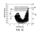
- Figures 12 and 13 illustrate plots of the
- Figure 12 provides plots of the
- Figure 13 provides an expanded view of the same plots 1210, 1220 within the active region of the SEL. Note that the antinodes 1211 of the
- the antinodes of the electric field substantially overlap with the quantum wells, and resonant periodic gain can occur in the gain structure that increases the efficiency of the device.
- DBRs formed of alternating layers of low and high refractive index materials that do not include gain structures (e.g., quantum wells) the antinodes of the electric field spontaneously occur at the interfaces between the high and low refractive index layers of the optical pairs.
- gain structures e.g., quantum wells
- Figure 15 shows portion of a symmetrical quantum well structure 1010 disposed between two spacer layers 1501, 1502.
- the quantum well structure 1510 includes two quantum wells 1521, 1522 with barriers 1511, 1512, 1513, wherein a barrier is arranged on either side of each quantum well 1521, 1522.
- the quantum well structure is referred to as "symmetrical" because the quantum wells 1521, 1522 are evenly spaced with respect to the center line 1005 of the quantum well structure 1510.
- the distance, d S-QW1 between the edge 1501a of a first spacer layer 1001 disposed on one side of the quantum well structure 1010 and an edge 1521a of a quantum well 1521 nearest to the spacer edge 1501a is substantially equal to the distance, d S-QW2 , between the edge 1502a of a second spacer layer 1502 disposed on another side of the quantum well structure 1510 and an edge 1522a of a quantum well 1522 nearest to the spacer edge 1502a.
- the resonant periodic gain condition occurs when the antinode 1551 of the electric field 1550 substantially aligns with the center line 1505.
- Figure 16 shows an asymmetrical quantum well structure 1610 disposed between two spacer layers 1501, 1502.
- the quantum well structure 1610 includes two quantum wells 1621, 1622 with barriers 1611, 1612, 1613 wherein a barrier is arranged on either side of each quantum well 1621, 1622.
- quantum wells near the interface between the quantum well structure and the spacer layer may have no barrier or a thin barrier, e.g., a barrier having a thickness less than the thickness of the other barriers in the quantum well structure.
- the quantum well structure is referred to as "asymmetrical" because the quantum wells 1621, 1622 are not evenly spaced with respect to the center line 1505 of the quantum well structure 1610.
- the thickness of at last two of the barriers 1611, 1612, 1613 is unequal.
- the thickness of at least one of the barriers is different from the thicknesses of the other barriers in the quantum well structure.
- the distance, d S-QW1 between the edge 1501a of a first spacer layer 1501 disposed on one side of the quantum well structure 1610 and an edge 1621a of a quantum well 1621 nearest to the spacer edge 1501a is not equal to the distance, d S-QW2 , between the edge 1502a of a second spacer layer 1502 disposed on another side of the quantum well structure 1610 and an edge 1622a of a quantum well 1622 nearest to the spacer edge 1502a.
- the resonant periodic gain condition occurs when the antinode 1651 of the electric field 1650 is shifted by an amount, ⁇ d, from the center line 1505.
- the geometry of the laser cavity may satisfy boundary conditions so that two optical modes are resonant in the laser cavity. These optical modes have nearly the same wavelength.
- SEL structures Two example SEL structures (examples 4 and 5) are discussed below and are illustrated in Figures 17 - 24 . These examples illustrate asymmetrical quantum well structures as well as phase shift layers.
- the quantum well thicknesses are selected to be about 5 nm with 50% Al composition in the quantum wells and with 60% Al composition in the barriers.
- Spacer layers may be disposed between quantum well structures. The spacer layers have 100% Al composition.
- a first 0.125 ⁇ phase shift element 1823-1 disposed between the first series 1801 of single quantum well structures and the series 1803 of double quantum well structures and a second 0.125 ⁇ phase shift element 1823-2 disposed between the series 1803 of double quantum well structures and the second series 1802 of single quantum well structures.
- the tenth single quantum well structure of the first series 1801 and the first single quantum well structure of the second series 1802 include phase shift layers 1823-1, 1823-2, respectively, and have optical thickness of 0.475 ⁇ .
- Each double quantum well structure with spacer layer 1825d has optical thickness 0.5 ⁇ .
- Figures 18 and 19 show plots of the
- the refractive index plot 1820 indicates various structures within the SEL. It can be observed, particularly in Figure 19 , that the asymmetry of the single quantum well structures 1821s in this example serves to align the quantum wells 1825 with the antinodes 1811 of the
- the SEL includes a substrate or template 1822 comprising AlN and having a refractive index of 2.319 at 266 nm, a physical thickness of 10000 ⁇ , and an optical thickness of 8.718 ⁇ .
- the SEL includes:
- the first series 1801 of single quantum well structures comprises layers 1 - 4 (9 times) and layers 5 - 7.
- the first series 1801 of single quantum well structures is followed by:
- the series 1803 of double quantum well structures includes layer 9 - 14 (repeated 9 times and layers 15 - 19.
- the series of double quantum well structures is followed by:
- the second series 1802 of single quantum well structures comprises layers 20 - 23 (repeated 9 times) plus layers 24 - 25.
- a phase shift element 2203 comprising a quadruple quantum well structure is disposed between the first 2201 and second 2202 series of fifteen 1.0 ⁇ DBR pairs with asymmetrical double quantum well structures (2221-1, 2221-2, Figure 22 ).
- Figures 22 and 23 show plots of the
- the refractive index plot 2220 indicates various structures within the SEL. It can be observed, particularly in Figure 23 , that the asymmetry of the double quantum well structures 2221-1, 2221-2 in this example serves to align the quantum wells 2225 with the antinodes 2211 of the
- the SEL includes a substrate or template 2222 comprising AlN and having a refractive index of 2.319 at 266 nm, a physical thickness of 10000 ⁇ , and an optical thickness of 8.718 ⁇ .
- the SEL includes:
- the second series of double quantum well structures comprises the last 14 repetitions of layers 12 - 17 plus layers 18 - 22.
- the phase shift layer comprises layers 7 - 11 plus the first repetition of layers 12 - 17.
- Figure 24 is a graph of the reflectivity of the structure of Figure 21 showing greater than 99% reflectivity at 266 nm.
- the DFB active zone as described herein can be used alone, without additional reflectors or gain elements. With a sufficient number of optical pairs, sufficient refractive index contrast between optical pairs, and sufficient number of gain structures, the DFB active zone can provide both acceptable optical feedback and optical gain for the DFB SEL, even when no additional reflectors and/or gain structures are employed.
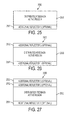
- the DFB active zone may be used in conjunction with one or more additional reflectors, as illustrated by the schematic diagrams of Figures 25 - 27.
- Figure 25 depicts an additional reflector 2551 disposed at one surface of the DFB active zone.
- This optional additional reflector 2551 may comprise a DBR having a number of optical pairs that provide additional reflectivity for the laser structure 2500.
- the optical pairs may comprise alternating lower refractive index/higher refractive index layers of an epitaxially grown semiconductor material, such as AlN/AlGaN and/or GaN/AlInN.
- Each layer of the optical pairs may have a geometrical thickness of ⁇ lase /4n, where n is the refractive index of the layer, and is non-absorptive for the lasing emission wavelength ⁇ lase .
- These optical pairs do not include quantum wells or other gain media, and thus provide only optical feedback and no optical gain.
- Figure 26 illustrates another configuration 2600 that employs additional reflectors 2551, 2552 that may be implemented along with a DFB active zone 2530.
- the DFB active zone is disposed between two additional reflectors 2551, 2552.
- both of the additional reflectors 2551, 2552 may comprise epitaxially grown DBRs as described in connection with Figure 25 .
- At least one of the reflectors 2551, 2552, e.g., reflector 2551 may comprise an epitaxially grown semiconductor DBR, and another of the reflectors, e.g., reflector 2552, may comprise a DBR formed from optical layer pairs comprising lower refractive index/higher refractive index layers of dielectric materials deposited on a surface of the DFB active zone, e.g., alternating TiO2/ SiO2 layers.
- Figure 27 includes a first optional reflector 2751 disposed at one side, e.g., the bottom side of the DFB active zone 2730 and second and third optional reflectors 2752, 2753 disposed at an opposite side, e.g., the top side of the DFB active zone 2730.
- the double top reflectors 2752, 2753 may be used without the bottom reflector 2751, the bottom reflector 2751 may be used without the double top reflectors 2752, 2753 and/or one or more reflectors in addition to reflector 2751 may be disposed at the bottom of the DFB active zone.
- the double reflectors may include at least one epitaxially grown semiconductor DBR, e.g., reflector 2752, and one deposited DBR comprising dielectric layers, e.g., reflector 2753.
- an excitation source can be used to excite the DFB active zone.
- multiple sources 2801 - 2804 can be used, as schematically illustrated in Figure 28 .
- the excitation sources 2801 - 2804 can be light sources that provide light to optically pump the DFB active zone 130.
- the pump light may be incident on the top surface of the laser, as illustrated in Figure 1 , and/or the semiconductor heterostructure may be etched to form a mesa structure 2800 as shown in Figure 28 with the light emitted from the pump sources 2801 - 2804 incident on the sides of the mesa.
- the mesa structure may be formed using chemical assisted ion beam etching (or other appropriate process) to etch away portions of the heterostructure, yielding a mesa structure 2800 having, for instance, a diameter of about 100 ⁇ m with an exposed sidewall.
- the mesa structure allows for a large solid angle to be accessed for pumping with pump sources 2801 - 2804 (e.g., high-brightness diode lasers).
- pump sources 2801 - 2804 e.g., high-brightness diode lasers.
- the light output of the laser diodes is collimated and focused onto the pillar like semiconductor mesa 2800.
- the cross-section of mesa (viewed axially) may be circular, or may have many other rectangular and non-rectangular cross sections.
- the electric field within the DFB active zone fluctuates between periods of higher electric field magnitude and periods of lower electric field magnitude.
- the DFB active zone can be arranged to take advantage of these fluctuations by placing quantum well structures at the locations within the DFB active zone having a higher electric field magnitude and/or by placing DBR pairs at locations within the DFB active zone having lower electric field magnitude.
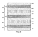
- Figure 29 illustrates another possible embodiment for the DFB active zone wherein optical pairs that include quantum well structure and spacer layers are not uniformly used throughout the DFB active zone.
- the DFB active zone includes at least some optical pairs comprising a no-gain, high refractive index layer and a spacer layer.
- the optical pairs comprising the quantum well structure and spacer layers may be disposed at locations within the DFB active zone having a higher electric field and the optical pairs comprising the no-gain, high refractive index layer and a spacer layer may be disposed at locations within the DFB active zone having a lower electric field.
- Figure 29 shows a DFB active zone that includes quantum well structure/spacer layer optical pairs that alternate with no-gain, high refractive index layer/spacer layer optical pairs.
- Figure 29 illustrates five optical pairs 2951 - 2955 in the DFB active zone.
- the first optical pair 2951 illustrated in Figure 29 comprises a spacer layer 2901 and a double quantum well structure 2911;
- the second optical pair 2952 comprises a spacer layer 2902 and a no-gain, high refractive index layer 2921;
- the third optical pair 2953 comprises a spacer layer 2903 and quantum well structure 2912;
- the fourth optical pair 2954 comprises a spacer layer 2904 and a no-gain, high refractive index layer 2922;
- the fifth optical pair 2955 comprises a spacer layer 1305 and quantum well structure 2913.
Landscapes
- Physics & Mathematics (AREA)
- Optics & Photonics (AREA)
- Condensed Matter Physics & Semiconductors (AREA)
- General Physics & Mathematics (AREA)
- Electromagnetism (AREA)
- Chemical & Material Sciences (AREA)
- Engineering & Computer Science (AREA)
- Nanotechnology (AREA)
- Life Sciences & Earth Sciences (AREA)
- Biophysics (AREA)
- Crystallography & Structural Chemistry (AREA)
- Semiconductor Lasers (AREA)
Abstract
Description
- Semiconductor lasers require optical gain, optical feedback, and a source of energy to initiate and sustain lasing. Surface emitting lasers (SELs) have recently been used as compact semiconductor lasers. Typically, in this type of laser, the laser light resonates between two reflective surfaces perpendicularly through the gain medium and the laser light is emitted perpendicularly to the laser surface. The two reflective surfaces of the laser, e.g. top and bottom distributed Bragg reflectors (DBRs), form the laser cavity and are separated by a thickness which is a multiple of half a wavelength of the laser light. The gain medium, which may comprise one or more quantum wells, for example, is arranged within the laser cavity. Energy is supplied to the gain medium by optical pumping or e-beam excitation, for example, creating holes and electrons that recombine within the gain medium to generate photons.
- Some embodiments involve a semiconductor surface emitting laser (SEL) that includes an active zone including quantum well structures separated by spacer layers. The quantum well structures are configured to provide optical gain for the SEL at a lasing wavelength, λlase. Each quantum well structure and an adjacent spacer layer are configured to form an optical pair of a distributed Bragg reflector (DBR), the active zone including a plurality of the DBR optical pairs and configured to provide optical feedback for the SEL at λlase.
- According to some aspects, λlase is in a range between about 250 nm and about 550 nm.
- According to some aspects, the SEL includes an optical pump source configured to emit pump light at pump wavelength, λpump to optically pump the SEL. In some cases, the pump source may be configured to provide in-well pumping of the SEL. In some cases, the pump source may be configured to provide barrier pumping of the SEL.
- According to some aspects, the SEL includes electron beam source configured to emit an electron beam as excitation source for the active zone of the SEL.
- In some implementations, the active zone comprises one or more mesa structures. optical pump source may be used to optically pump the SEL side walls of the one or more mesa structures.
- According to some aspects, one or more additional DBRs are used that do not provide optical gain disposed adjacent to the active zone. For example, the one or more additional DBRs may comprise only one DBR.
- According to some aspects, the active zone includes one or more first optical pairs that provide the optical gain and the optical feedback interspersed with one or more second optical pairs that provide the optical gain without providing the optical feedback.
- According to some aspects, the active zone includes one or more first optical pairs that provide the optical gain and the optical feedback interspersed with one or more third optical pairs that provide the optical feedback without providing the optical gain.
- In some embodiments, the active zone includes at least one phase shift element, the phase shift element configured to shift a phase of an optical mode present within the active zone during operation of the SEL. For example, the phase shift element may comprise an optical gain element.
- Some embodiments involve a surface emitting laser (SEL), comprising an active zone including quantum well structures, each quantum well structure including one or more quantum wells comprising AlxGa1-xN. The quantum well structures are separated by spacer layers comprising AlyGa1-yN, where y > x The quantum well structures are configured to provide optical gain for the SEL at a lasing wavelength, λlase Each quantum well structure and an adjacent spacer layer are configured to form an optical pair of a distributed Bragg reflector (DBR. Each quantum well structure provides a high refractive index portion of the optical pair and the spacer layer provides a low refractive index portion of the optical pair. The DBR includes a plurality of the optical pairs and provides optical feedback for the SEL at a lasing wavelength, λlase.
- According to some aspects, a number of the optical pairs is sufficient to provide a reflectivity of greater than about 98% at λlase.
- According to some aspects, the active zone is epitaxially grown on a bulk AlN substrate.
- Some embodiments involve a semiconductor surface emitting laser (SEL), comprising an active zone including quantum well structures separated by spacer layers. The quantum well structures are configured to provide optical gain for the SEL at a lasing wavelength, λlase. Each quantum well structure and an adjacent spacer layer are configured to form an optical pair of a distributed Bragg reflector (DBR). The active zone includes a plurality of the DBR optical pairs and provides optical feedback for the SEL at λlase. At least some of the quantum well structures are asymmetrical, each asymmetrical quantum well structure having one or more quantum wells and one or more barriers and the one or more quantum wells are not centered between spacer layers adjacent to the quantum well structure.
- For example, in some implementations substantially all of the quantum well structures are asymmetrical.
- Some implementations include one or more additional DBRs that do not provide optical gain and which are disposed adjacent to the active zone. The one or more additional DBRs may comprise only one DBR.
- Some embodiments involve a semiconductor surface emitting laser (SEL). The active zone of the SEL means for providing optical gain for the SEL at a lasing wavelength, λlase and means for providing optical feedback for the SEL at λlase. The means for providing optical gain and the means for providing optical feedback are distributed throughout the active region.
-
-
Figure 1 is a schematic cross sectional diagram of a distributed feedback surface emitting laser (DFB SEL) comprising a distributed feedback (DFB) active zone that provides both optical gain and optical feedback to the laser emission according to various embodiments; -
Figure 2 is a schematic cross sectional view that shows in more detail the DFB active zone of the DFB SEL ofFigure 1 ; -
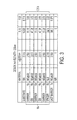
Figure 3 illustrates the structure of an exemplary DFB SEL design for a lasing wavelength λ = 266 nm that uses sixteen 0.5 λ double quantum well structures; -
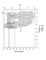
Figures 4 and5 illustrate plots of the |E|2 electrical field and refractive index in the DFB active zone of the SEL structure ofFigure 3 ; -
Figure 6 shows the reflectivity spectra for the DFB SEL ofFigure 3 ; -
Figure 7 illustrates the structure of an exemplary DFB SEL design for a lasing wavelength λ = 266 nm that uses thirty 1.0 λ single quantum well structures; -
Figures 8 and 9 illustrate plots of the |E|2 electrical field and refractive index in the DFB active zone of the SEL structure ofFigure 7 ; -
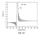
Figure 10 shows the reflectivity spectra for the DFB SEL ofFigure 7 ; -
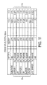
Figure 11 illustrates the structure of an exemplary DFB SEL design for a lasing wavelength λ = 266 nm that uses twenty 1.5 λ double quantum well structures; -
Figures 12 and13 illustrate plots of the |E|2 electrical field and refractive index in the DFB active zone of the SEL structure ofFigure 11 ; -
Figure 14 shows the reflectivity spectra for the DFB SEL ofFigure 11 ; -
Figure 15 shows a symmetrical quantum well structure disposed between two spacer layers; -
Figure 16 shows an asymmetrical quantum well structure disposed between two spacer layers; -
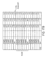
Figures 17A - 17B illustrate the structure of an exemplary DFB SEL design that includes phase shift structures; -
Figures 18 and 19 illustrate plots of the |E|2 electrical field and refractive index in the DFB active zone of the SEL structure ofFigures 17A - 17B ; -
Figure 20 shows the reflectivity spectra for the DFB SEL ofFigures 17A - 17B ; -
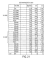
Figure 21 illustrates the structure of an exemplary DFB SEL design that includes a phase shift structure; -
Figures 22 and 23 illustrate plots of the |E|2 electrical field and refractive index in the DFB active zone of the SEL structure ofFigure 21 ; -
Figure 24 shows the reflectivity spectra for the DFB SEL ofFigure 21 ; -
Figure 25 depicts a DFB SEL that includes an additional reflector disposed at one surface of the DFB active zone; -
Figure 26 illustrates a configuration wherein the DFB active zone is disposed between two additional reflectors; -
Figure 27 depicts the use of two types of reflectors disposed at one or both sides of the DFB active zone; -
Figure 28 illustrates a DFB SEL etched in a mesa structure and excited by multiple pump sources; and -
Figure 29 shows a DFB active zone that includes quantum well structure/spacer layer optical pairs that alternate with no-gain, high refractive index layer/spacer layer optical pairs. - Like reference numbers in the various drawings refer to like structures.
- Embodiments discussed herein involve distributed feedback SELs (DFB SELs) that include a distributed feedback (DFB) active zone that provides both optical gain and optical feedback for the laser. In the embodiments described herein, both the optical gain and optical feedback provided by the DFB SEL active zone are distributed throughout the active zone. In some embodiments, the DFB SELs described herein rely on one DFB active zone comprising a heterostructure including multiple pairs of gain structures alternating with spacer layers. This heterostructure provides both the optical gain and the optical feedback for the laser and no additional reflectors are used to provide optical feedback and/or no additional gain elements to provide optical gain are used. In some embodiments, a DFB active zone that combines the functions of optical gain and optical feedback is used in combination with additional reflectors and/or additional gain elements.
- Combining the optical gain and optical feedback functions into one DFB active zone significantly reduces the complexity of the laser heterostructure and can increase the overall performance. In some embodiments, the laser does not need any additional reflector beyond the reflector provided by the DFB active zone itself. The DFB SEL embodiments discussed herein facilitate the realization of single longitudinal mode semiconductor lasers.
-
Figure 1 shows aDFB SEL 100 that includes a DFBactive zone 130 that provides both optical gain and optical feedback to thelaser 100. The DFBactive zone 130 can be epitaxially grown on acompatible substrate 110. Anexcitation source 150 provides energy to the active zone to facilitate lasing. In some embodiments, thesource 150 comprises an optical source that provides pump light 155 to theactive zone 130. In general, thepump light 155 is supplied at a shorter wavelength than the emittedlaser light 160. In some cases, thepump light 155 may be incident on the laser surface at an angle, θ, with respect to the vector normal 101 to the laser surface. The wavelength and angle of the pump light may be selected to provide in-well or barrier pumping, for example. In some embodiments, the excitation source may comprise an electron beam source configured to direct a beam of electrons towards thelaser 100 to excite the DFB active zone. - The DFB
active zone 130 provides both optical gain and optical feedback for thelaser 100. The DFB active zone includes multiple quantum well structures separated by spacer layers. The quantum well structures include one or more quantum wells that provide optical gain for the laser. Each quantum well structure and an adjacent spacer layer are designed so that they function as an optical pair of a distributed Bragg reflector, wherein the distributed Bragg reflector provides the optical feedback for the laser. Thus, the quantum wells of the quantum well structure of each optical pair provide optical gain for the laser while the combination of the quantum well structure and adjacent spacer layer provide optical feedback. - Although the DFB active zone and other semiconductor portions of the
laser 100 may be formed from any suitable semiconductor, in some embodiments, the DFB active zone is based on a III-nitride material system, e.g. AlGaN, AlInN, GaInN, AlGaInN, and/or other such materials. The DFB active zone and/or other semiconductor layers can be epitaxially grown on a bulk aluminum nitride (AlN), a gallium nitride (GaN) substrate, or other suitable substrate. In some cases, the DFB active zone and/or other semiconductor layers can be grown on an AlN, AlGaN, GaInN or GaN template disposed on a substrate of Al2O3 (sapphire) or other compatible material. -
Figure 2 is a schematic cross sectional view that shows in more detail the DFBactive zone 130 of thelaser 100 ofFigure 1 .Optical pairs structures structures - In some cases, the quantum well
structures structures optical pair optical pair - As illustrated in
Figure 2 , the quantum wellstructures quantum well spacer layer barrier structures Figure 2 each include twoquantum wells Figure 2 , thequantum wells quantum well structure Figure 2 , all of thebarriers structures quantum wells structures - In some cases, each layer section of the optical pairs, which is the quantum well structure and the spacer layer, has a geometrical thickness of λlase/4n, where λlase is the wavelength of the laser light in vacuum and n is the refractive index of the layer. For homogeneous spacer layers (a homogeneous spacer layer is one that has the same material throughout the spacer layer), the geometrical thickness is λlase/4nS, where nS is the refractive index of the spacer material. The geometrical thickness of the quantum well structures is λlase/4neff, and can be calculated for a symmetrical quantum well structure as:

- For example, consider the active zone of
Figure 2 , designed for laser light having a wavelength λlase = 266 nm, with AlN spacer layers, and symmetrical quantum well structures comprising 4.7 nm Al0.5Ga0.5N quantum wells, and 5.1 nm Al0.6Ga0.4N barriers. The geometrical thickness of the spacer layers is 266 nm/4* 2.319 = 28.7 nm, where 2.319 is the refractive index of AlN at λ = 266 nm. The geometrical thickness of the quantum well structure is 266nm/4neff. In this example, the refractive index of Al0.5Ga0.5N at 266 nm is 2.813 and the refractive index of Al0.6Ga0.4N at 266 nm is 2.583. Thus, neff = ((2*4.7nm*2.813) + (3*5.1*2.583))/(2*4.7 + 3*5.1) = 2.670. - In
Figure 2 , theactive zone 130 is arranged to provide resonant periodic gain wherein the antinodes of the standing wave electrical field substantially overlap or coincide with the quantum well gain structures. The quantum well structures are spaced at a multiple of one half the laser light wavelength to achieve the resonant periodic gain configuration. The periodicity of the resonant periodic gain configuration, wherein the antinodes of the standing-wave field of the laser light substantially coincide with the quantum well structures, provides a significant increase in the optical gain when compared with similar structures that are non-resonant. - In some optically pumped embodiments, the laser structure is configured such that resonance is achieved at both the laser light and pump light wavelengths to provide both resonant periodic gain by the laser light and resonance enhanced absorption of the pump light. Resonance enhanced absorption occurs when the antinodes of the pump light electromagnetic field substantially coincide with the structures that absorb the pump light. Resonant enhanced absorption can be achieved in two ways. One approach to achieve resonance enhanced absorption involves the use of a laser cavity thickness for which resonances exist at both the pump light wavelength and the laser light wavelength. Another approach to achieve resonance enhanced absorption is to use an off-normal incidence angle for the pump light beam. For example, as shown in
Figure 1 , thepump light 155 may be incident on the surface of thelaser 100 at an off normal incidence angle of θ. The use of resonance enhanced absorption for laser structures is described in commonly ownedU.S. Patent 8,000,371 . - The optimal number of optical pairs in the DFB active zone is dependent on the reflectivity of the DFB active zone that in turn is dependent on the refractive index contrast between the layers of the optical pairs. In general, a suitable reflectivity for the DFB active zone is greater than about 98%. For the example discussed above (28.7 nm AlN spacer layers, 4.7 nm Al0.5Ga0.5N quantum wells, and 5.1 nm Al0.6Ga0.4N barriers), a suitable number of optical pairs to achieve suitable reflectivity, e.g., greater than about 98%, may range between about 15 and about 30 optical pairs.
- Three example SEL structures are discussed below and are illustrated in
Figures 3 -14. In examples 1 - 3, a number of quantum well structures are disposed between a substrate and a final barrier and the lasing wavelength is λ = 266 nm. In each example, the quantum well thicknesses are selected to be about 5 nm with 50% Al composition in the quantum wells and with 60% Al composition in the barriers. In each case, a spacer layer is disposed between the quantum well structures. The spacer layers have 100% Al composition. The period thicknesses for the three examples are 0.5 λ, 1.0 λ, and 1.5 λ, respectively, where the refractive index is used to determine the physical thicknesses of the layers. In examples 1 and 2, the last barriers have a thickness of 0.25 λ for high reflectivity, although other thicknesses for the last barrier may be used. For example, in example 3, the last barrier has a thickness of 0.375 λ. The use of a double quantum well structure requires fewer optical pairs to achieve the same reflectivity, leading to a thinner overall thickness for the SEL which is beneficial to keep growth times relatively short and to not exceed the critical thickness. In examples 1 - 3, reflectivity greater than 98% is achieved. -
Figure 3 illustrates the structure of an exemplary DFB SEL design for a lasing wavelength λ = 266 nm that uses sixteen 0.5 λ double quantum well structures (see, 421,Figure 5 ). In the illustrated example, the SEL includes a substrate or template (see, 422,Figure 5 ) comprising AlN and having a refractive index of 2.319 at 266 nm. For the simulation a physical thickness of 10000 Å was chosen. The SEL includes a last barrier (423,Figure 5 ) comprising Al0.6G0.4N having a refractive index of 2.583 at 266 nm, a physical thickness of 386.2 Å, and an optical thickness of 0.375 λ. Sixteen repeating double quantum well structures (421,Figure 5 ) are disposed between thesubstrate 422 and thelast barrier 423. Each DBR pair has an optical thickness of 0.5 λ and includes the following layers in order: - 1. Al0.6Ga0.4N barrier (424,
Figure 5 ) having a refractive index of 2.583 at 266 nm, a physical thickness of 51.49 Å, and an optical thickness of 0.05λ; - 2. Al0.5Ga0.5N quantum well (425,
Figure 5 ) having a refractive index of 2.813 at 266 nm, a physical thickness of 47.28 Å, and an optical thickness of 0.05λ; - 3. Al0.6Ga0.4N barrier (424,
Figure 5 ) having a refractive index of 2.583 at 266 nm, a physical thickness of 51.49 Å, and an optical thickness of 0.05λ; - 4. Al0.5Ga0.5N quantum well (425,
Figure 5 ) having a refractive index of 2.813 at 266 nm, a physical thickness of 47.28 Å, and an optical thickness of 0.05λ; - 5. Al0.6Ga0.4N barrier (424,
Figure 5 ) having a refractive index of 2.583 at 266 nm, a physical thickness of 51.49 Å, and an optical thickness of 0.05λ; - 6. AlN spacer layer (426,
Figure 5 ) having a refractive index of 2.319 at 266 nm, a physical thickness of 286.8 Å, and an optical thickness of 0.25λ. -
Figures 4 and5 illustrate plots of the |E|2electrical field 410 andrefractive index 420 in the DFB active zone of the SEL structure ofFigure 3 .Figure 4 provides plots of the |E|2electrical field 410 andrefractive index 420 within the SEL from 0 to 2µm (at the last barrier).Figure 5 provides an expanded view of thesame plots antinodes 411 of theelectric field 410 substantially coincide with the quantum wellstructures 421 providing resonant periodic gain as previously discussed.Figure 6 provides agraph 610 of the reflectivity of the structure ofFigure 3 indicating a reflectivity over 98% at the lasing wavelength λ = 266 nm. -
Figure 7 illustrates the structure of an exemplary DFB SEL design for a lasing wavelength λ = 266 nm that uses thirty 1.0 λ single quantum well structures (821, seeFigure 8 ). In the illustrated example, the SEL includes an AlN substrate or template (822,Figure 8 ) that has a refractive index of 2.319 at 266 nm, a physical thickness of 10000 Å, and an optical thickness of 8.718 λ. The SEL includes a last barrier (823,Figure 8 ) comprising Al0.6G0.4N having a refractive index of 2.583 at 266 nm, a physical thickness of 386.2 Å, and an optical thickness of 0.375 λ. Thirty repeating single quantum wellstructures 821 are disposed between thesubstrate 822 and thelast barrier 823. Each DBR pair has an optical thickness of 0.5 λ and includes the following layers in order: - 1. Al0.6Ga0.4N barrier (824,
Figure 8 ) having a refractive index of 2.83 at 266 nm, a physical thickness of 360.4 Å, and an optical thickness of 0.35λ; - 2. Al0.5Ga0.5N quantum well (825,
Figure 8 ) having a refractive index of 2.583 at 266 nm, a physical thickness of 47.28 Å, and an optical thickness of 0.05λ; - 3. Al0.6Ga0.4N barrier (824,
Figure 8 ) having a refractive index of 2.83 at 266 nm, a physical thickness of 360.4 Å, and an optical thickness of 0.35λ; - 4. AlN spacer layer (826,
Figure 8 ) having a refractive index of 2.319 at 266 nm, a physical thickness of 286.8 Å, and an optical thickness of 0.25λ. -
Figures 8 and 9 illustrate plots of the |E|2electrical field 810 andrefractive index 820 in the DFB active zone of a SEL.Figure 8 provides plots of the |E|2electrical field 810 andrefractive index 820 within the SEL from 0 to 5µm.Figure 9 provides an expanded view of thesame plots antinodes 811 of theelectric field 810 substantially coincide with the quantum wellstructures 821 providing resonant periodic gain as previously discussed.Figure 10 provides agraph 1010 of the reflectivity of the structure ofFigure 7 indicating a reflectivity over 98% at the lasing wavelength, λ = 266 nm. -
Figure 11 illustrates the structure of an exemplary DFB SEL design for a lasing wavelength λ = 266 nm that uses twenty 1.5 λ double quantum well structures (1221,Figure 13 ). In the illustrated example, two thicker barriers (1224,Figure 13 ) are used on either side of the quantum wells (1225,Figure 13 ) and one thin barrier (1226,Figure 13 ) is used between thequantum wells 1221. The SEL includes a substrate (1222,Figure 13 ) comprising AlN and having a refractive index of 2.319 at 266 nm, a physical thickness of 10000 Å, and an optical thickness of 8.718 λ. The SEL includes a last barrier (1223,Figure 12 ) comprising Al0.6G0.4N having a refractive index of 2.583 at 266 nm, a physical thickness of 579.3 Å, and an optical thickness of 0.5625 λ. Twenty repeating doublequantum well structures 1221 are disposed between thesubstrate 1222 and thelast barrier 1223. Each DBR pair has an optical thickness of 1.5 λ and includes the following layers in order: - 1. Al0.6Ga0.4N thick barrier (1224,
Figure 13 ) having a refractive index of 2.583 at 266 nm, a physical thickness of 502.1 Å, and an optical thickness of 0.4875λ; - 2. Al0.5Ga0.5N quantum well (1225,
Figure 13 ) having a refractive index of 2.813 at 266 nm, a physical thickness of 47.28 Å, and an optical thickness of 0.05λ; - 3. Al0.6Ga0.4N thin barrier (1227,
Figure 13 ) having a refractive index of 2.583 at 266 nm, a physical thickness of 51.49 Å, and an optical thickness of 0.05λ; - 4. Al0.5Ga0.5N quantum well (1225,
Figure 13 ) having a refractive index of 2.813 at 266 nm, a physical thickness of 47.28 Å, and an optical thickness of 0.05λ; - 5. Al0.6Ga0.4N thick barrier (1224,
Figure 13 ) having a refractive index of 2.583 at 266 nm, a physical thickness of 502.1 Å, and an optical thickness of 0.4875λ; - 6. AlN spacer layer (1226,
Figure 13 ) having a refractive index of 2.319 at 266 nm, a physical thickness of 430.1 Å, and an optical thickness of 0.375λ. -
Figures 12 and13 illustrate plots of the |E|2electrical field 1210 andrefractive index 1220 in the DFB active zone of the SEL ofFigure 11 .Figure 12 provides plots of the |E|2electrical field 1210 andrefractive index 1220 within the SEL from 0 to 5 µm.Figure 13 provides an expanded view of thesame plots antinodes 1211 of the |E|2electrical field 1210 substantially coincide with thequantum well structures 1221 providing resonant periodic gain as previously discussed.Figure 14 provides agraph 1410 of the reflectivity of the structure ofFigure 11 indicating a reflectivity of 98.0% at the lasing wavelength λ = 266 nm. - Referring back to
Figure 2 , when the device has a design that satisfies certain boundary conditions, the antinodes of the electric field substantially overlap with the quantum wells, and resonant periodic gain can occur in the gain structure that increases the efficiency of the device. In DBRs formed of alternating layers of low and high refractive index materials that do not include gain structures (e.g., quantum wells) the antinodes of the electric field spontaneously occur at the interfaces between the high and low refractive index layers of the optical pairs. In a DFB active zone, there can be some distance between the antinode position in the quantum well structure that satisfies the condition for resonant periodic gain and the interface between the high and low refractive index layers. It can be useful to design the quantum well structure so that the distance between the antinode position within the quantum well structure that provides the optimal resonant periodic gain and the interface between the high and low refractive index layers is decreased. Decreasing the distance between the optimal antinode position for resonant periodic gain and the interface can be accomplished using asymmetrical quantum well structures as described in more detail below in connection withFigures 15 and 16 . -
Figure 15 shows portion of a symmetricalquantum well structure 1010 disposed between twospacer layers quantum well structure 1510 includes twoquantum wells barriers quantum well quantum wells quantum well structure 1510. The thickness of thebarriers edge 1501a of a first spacer layer 1001 disposed on one side of thequantum well structure 1010 and anedge 1521a of a quantum well 1521 nearest to thespacer edge 1501a is substantially equal to the distance, dS-QW2, between theedge 1502a of asecond spacer layer 1502 disposed on another side of thequantum well structure 1510 and anedge 1522a of a quantum well 1522 nearest to thespacer edge 1502a. As can be appreciated fromFigure 15 , for a symmetrical quantum well structure, the resonant periodic gain condition occurs when the antinode 1551 of theelectric field 1550 substantially aligns with thecenter line 1505. -
Figure 16 shows an asymmetricalquantum well structure 1610 disposed between twospacer layers quantum well structure 1610 includes twoquantum wells barriers quantum well quantum wells center line 1505 of thequantum well structure 1610. The thickness of at last two of thebarriers edge 1501a of afirst spacer layer 1501 disposed on one side of thequantum well structure 1610 and anedge 1621a of a quantum well 1621 nearest to thespacer edge 1501a is not equal to the distance, dS-QW2, between theedge 1502a of asecond spacer layer 1502 disposed on another side of thequantum well structure 1610 and anedge 1622a of a quantum well 1622 nearest to thespacer edge 1502a. As can be appreciated fromFigure 16 , for an asymmetrical quantum well structure, the resonant periodic gain condition occurs when the antinode 1651 of theelectric field 1650 is shifted by an amount, Δd, from thecenter line 1505. - In the asymmetrical cases, each layer of the quantum well structure/spacer optical pairs may have a geometrical thickness of λlase/4n, where λlase is the wavelength of the laser light and n is the refractive index of the layer. In some embodiments, the geometrical thickness of the spacer layers is λlase/4nS, where nS is the refractive index of the spacer material. In these embodiments, the geometrical thickness of the quantum well structures is λlase/4neff, where neff can be calculated for an asymmetrical quantum well structure as:

where K is the total number of quantum wells in the quantum well structure, d QWk is the thickness of the kth quantum well, nQW is the refractive index of the quantum wells, J is the total number of barriers in the quantum well structure, dBARj is the thickness of the jth barrier, and nBAR is the refractive index of the barriers. - In some configurations, the geometry of the laser cavity may satisfy boundary conditions so that two optical modes are resonant in the laser cavity. These optical modes have nearly the same wavelength. In these configurations, it can be helpful to include phase shift layers in the laser structure to reduce the possibility of these competitive optical modes. These phase shift layers operate to provide single mode operation in many cases.
- Two example SEL structures (examples 4 and 5) are discussed below and are illustrated in
Figures 17 - 24 . These examples illustrate asymmetrical quantum well structures as well as phase shift layers. In examples 4 and 5, a number of quantum well structures are disposed on a substrate and the lasing wavelength is λ = 266 nm. In each example, the quantum well thicknesses are selected to be about 5 nm with 50% Al composition in the quantum wells and with 60% Al composition in the barriers. Spacer layers may be disposed between quantum well structures. The spacer layers have 100% Al composition. -
Figures 17A - 17B illustrate the structure of an exemplary DFB SEL design for a lasing wavelength λ = 266 nm that uses a series (1803,Figure 18 ) of ten symmetrical double quantum well structures (1821d,Figure 18 ) disposed between first 1801 and second 1802 series of ten asymmetrical single quantum well structures (1821s,Figure 18 ). A first 0.125 λ phase shift element 1823-1 disposed between thefirst series 1801 of single quantum well structures and theseries 1803 of double quantum well structures and a second 0.125 λ phase shift element 1823-2 disposed between theseries 1803 of double quantum well structures and thesecond series 1802 of single quantum well structures. Nine quantum well structures with spacer layers of the first andsecond series first series 1801 and the first single quantum well structure of thesecond series 1802 include phase shift layers 1823-1, 1823-2, respectively, and have optical thickness of 0.475λ. Each double quantum well structure with spacer layer 1825d has optical thickness 0.5 λ. -
Figures 18 and 19 show plots of the |E|2electrical field 1810 andrefractive index 1820 within the SEL from 0 to 2.6 µm (after the last quantum well structure). Therefractive index plot 1820 indicates various structures within the SEL. It can be observed, particularly inFigure 19 , that the asymmetry of the singlequantum well structures 1821s in this example serves to align thequantum wells 1825 with theantinodes 1811 of the |E|2electrical field 1810.Figure 20 provides agraph 2010 of the reflectivity of the structure ofFigures 17A - 17B indicating a reflectivity of greater than 99% at the lasing wavelength λ = 266 nm. - In the illustrated example, the SEL includes a substrate or
template 1822 comprising AlN and having a refractive index of 2.319 at 266 nm, a physical thickness of 10000 Å, and an optical thickness of 8.718 λ. The SEL includes: - 1. Al0.6Ga0.4N thin barrier (1831,
Figure 18 ) having a refractive index of 2.583 at 266 nm, a physical thickness of 51.49 Å, and an optical thickness of 0.05 λ; - 2. Al0.5Ga0.5N quantum well (1825,
Figure 13 ) having a refractive index of 2.813 at 266 nm, a physical thickness of 47.28 Å, and an optical thickness of 0.05λ; - 3. Al0.6Ga0.4N thick barrier (1832,
Figure 18 ) having a refractive index of 2.583 at 266 nm, a physical thickness 154.47 Å (3 x 51.49 Å, and an optical thickness of 0.15λ (3 x 0.05λ); - 4. AlN spacer layer (1826,
Figure 18 ) having a refractive index of 2.319 at 266 nm, a physical thickness of 286.8 Å, and an optical thickness of 0.25λ. - Layers 1 - 4 are repeated 9 times followed by:
- 5. Al0.6Ga0.4N thin barrier (1831,
Figure 18 ) having a refractive index of 2.583 at 266 nm, a physical thickness of 51.49 Å, and an optical thickness of 0.05 λ; - 6. Al0.5Ga0.5N quantum well (1825,
Figure 13 ) having a refractive index of 2.813 at 266 nm, a physical thickness of 47.28 Å, and an optical thickness of 0.05λ; - 7. Al0.6Ga0.4N thick barrier (1832,
Figure 18 ) having a refractive index of 2.583 at 266 nm, a physical thickness 154.47 Å (3 x 51.49 Å), and an optical thickness of 0.15λ (3 x 0.05 λ). - The
first series 1801 of single quantum well structures comprises layers 1 - 4 (9 times) and layers 5 - 7. Thefirst series 1801 of single quantum well structures is followed by: - 8. AlN phase shift element (1823-1,
Figure 18 ) having a refractive index of 2.319 at 266 nm, a physical thickness of 143.4 Å, and an optical thickness of 0.125λ; - 9. Al0.6Ga0.4N thin barrier (1831,
Figure 18 ) having a refractive index of 2.583 at 266 nm, a physical thickness of 51.49 Å, and an optical thickness of 0.05λ; - 10. Al0.5Ga0.5N quantum well (1825,
Figure 18 ) having a refractive index of 2.813 at 266 nm, a physical thickness of 47.28 Å, and an optical thickness of 0.05λ; - 11. Al0.6Ga0.4N thin barrier (1831,
Figure 18 ) having a refractive index of 2.583 at 266 nm, a physical thickness of 51.49 Å, and an optical thickness of 0.05λ; - 12. Al0.5Ga0.5N quantum well (1825,
Figure 18 ) having a refractive index of 2.813 at 266 nm, a physical thickness of 47.28 Å, and an optical thickness of 0.05λ; - 13. Al0.6Ga0.4N thin barrier (1831,
Figure 18 ) having a refractive index of 2.583 at 266 nm, a physical thickness of 51.49 Å, and an optical thickness of 0.05λ; - 14. AlN spacer layer (1826,
Figure 18 ) having a refractive index of 2.319 at 266 nm, a physical thickness of 286.8 Å, and an optical thickness of 0.25λ. - Layers 9 - 14 are repeated nine times, followed by:
- Al0.6Ga0.4N thin barrier (1831,
Figure 18 ) having a refractive index of 2.583 at 266 nm, a physical thickness of 51.49 Å, and an optical thickness of 0.05λ; - 15. Al0.5Ga0.5N quantum well (1825,
Figure 18 ) having a refractive index of 2.813 at 266 nm, a physical thickness of 47.28 Å, and an optical thickness of 0.05λ; - 16. Al0.6Ga0.4N thin barrier (1831,
Figure 18 ) having a refractive index of 2.583 at 266 nm, a physical thickness of 51.49 Å, and an optical thickness of 0.05λ; - 17. Al0.5Ga0.5N quantum well (1825,
Figure 18 ) having a refractive index of 2.813 at 266 nm, a physical thickness of 47.28 Å, and an optical thickness of 0.05λ; - 18. Al0.6Ga0.4N thin barrier (1831,
Figure 18 ) having a refractive index of 2.583 at 266 nm, a physical thickness of 51.49 Å, and an optical thickness of 0.05λ. - The
series 1803 of double quantum well structures includes layer 9 - 14 (repeated 9 times and layers 15 - 19. The series of double quantum well structures is followed by: - 19. AlN phase shift element (1823-2,
Figure 18 ) having a refractive index of 2.319 at 266 nm, a physical thickness of 143.4 Å, and an optical thickness of 0.125λ; - 20. Al0.6Ga0.4N thick barrier (1832,
Figure 18 ) having a refractive index of 2.583 at 266 nm, a physical thickness 154.47 Å (3 x 51.49 Å), and an optical thickness of 0.15λ (3 x 0.05λ); - 21. Al0.5Ga0.5N quantum well (1825,
Figure 13 ) having a refractive index of 2.813 at 266 nm, a physical thickness of 47.28 Å, and an optical thickness of 0.05λ; - 22. Al0.6Ga0.4N thin barrier (1831,
Figure 18 ) having a refractive index of 2.583 at 266 nm, a physical thickness of 51.49 Å, and an optical thickness of 0.05 λ; - 23. AlN spacer layer (1826,
Figure 18 ) having a refractive index of 2.319 at 266 nm, a physical thickness of 286.8 Å, and an optical thickness of 0.25λ. - Layers 20 - 23 are repeated 9 times followed by:
- 24. Al0.6Ga0.4N thick barrier (1832,
Figure 18 ) having a refractive index of 2.583 at 266 nm, a physical thickness 154.47 Å (3 x 51.49 Å), and an optical thickness of 0.15λ (3 x 0.05λ). - 25. Al0.5Ga0.5N quantum well (1825,
Figure 13 ) having a refractive index of 2.813 at 266 nm, a physical thickness of 47.28 Å, and an optical thickness of 0.05λ; - 26. Al0.6Ga0.4N thin barrier (1831,
Figure 18 ) having a refractive index of 2.583 at 266 nm, a physical thickness of 51.49 Å, and an optical thickness of 0.05 λ. - The
second series 1802 of single quantum well structures comprises layers 20 - 23 (repeated 9 times) plus layers 24 - 25. -
Figure 21 illustrates the structure of an exemplary DFB SEL design for a lasing wavelength λ = 266 nm that uses a first series (2201,Figure 22 ) of fifteen 1.0λ DBR pairs with asymmetrical double quantum well structures (2221-1,Figure 22 ) and a second series (2202,Figure 22 ) of fifteen 1.0λ DBR pairs with asymmetrical double quantum well structures (2221-2,Figure 22 ). Aphase shift element 2203 comprising a quadruple quantum well structure is disposed between the first 2201 and second 2202 series of fifteen 1.0λ DBR pairs with asymmetrical double quantum well structures (2221-1, 2221-2,Figure 22 ). -
Figures 22 and 23 show plots of the |E|2electrical field 2210 andrefractive index 2220 within the SEL from 0 to 2.6 µm (after the last quantum well structure). Therefractive index plot 2220 indicates various structures within the SEL. It can be observed, particularly inFigure 23 , that the asymmetry of the double quantum well structures 2221-1, 2221-2 in this example serves to align thequantum wells 2225 with theantinodes 2211 of the |E|2electrical field 2210. - In the illustrated example, the SEL includes a substrate or
template 2222 comprising AlN and having a refractive index of 2.319 at 266 nm, a physical thickness of 10000 Å, and an optical thickness of 8.718 λ. The SEL includes: - 1. Al0.6Ga0.4N thick barrier (2231,
Figure 22 ) having a refractive index of 2.583 at 266 nm, a physical thickness of 434.3 Å, and an optical thickness of 0.425λ; - 2. Al0.5Ga0.5N quantum well (2225,
Figure 22 ) having a refractive index of 2.813 at 266 nm, a physical thickness of 46.92 Å, and an optical thickness of 0.05λ; - 3. Al0.6Ga0.4N thin barrier (1232,
Figure 22 ) having a refractive index of 2.583 at 266 nm, a physical thickness 51.1 Å and an optical thickness of 0.05λ; - 4. Al0.5Ga0.5N quantum well (2225,
Figure 22 ) having a refractive index of 2.813 at 266 nm, a physical thickness of 46.92 Å, and an optical thickness of 0.05λ; - 5. Al0.6Ga0.4N medium barrier (2233,
Figure 22 ) having a refractive index of 2.583 at 266 nm, a physical thickness of 178.9 Å, and an optical thickness of 0.175λ; - 6. AlN spacer layer (2226,
Figure 22 ) having a refractive index of 2.319 at 266 nm, a physical thickness of 284.6 Å, and an optical thickness of 0.25λ. - The first series of double quantum well structures comprises layers 1 - 6 repeated 15 times. Layers 1 - 6 repeated 15 times are followed by:
- 7. Al0.6Ga0.4N thick barrier (2231,
Figure 22 ) having a refractive index of 2.583 at 266 nm, a physical thickness of 434.3 Å, and an optical thickness of 0.425λ; - 8. Al0.5Ga0.5N quantum well (2225,
Figure 22 ) having a refractive index of 2.813 at 266 nm, a physical thickness of 46.92 Å, and an optical thickness of 0.05λ; - 9. Al0.6Ga0.4N thin barrier (1232,
Figure 22 ) having a refractive index of 2.583 at 266 nm, a physical thickness 51.1 Å and an optical thickness of 0.05λ; - 10. Al0.5Ga0.5N quantum well (2225,
Figure 22 ) having a refractive index of 2.813 at 266 nm, a physical thickness of 46.92 Å, and an optical thickness of 0.05λ; - 11. Al0.6Ga0.4N medium barrier (2233,
Figure 22 ) having a refractive index of 2.583 at 266 nm, a physical thickness of 178.9 Å, and an optical thickness of 0.175λ; - 12. Al0.6Ga0.4N medium barrier (2233,
Figure 22 ) having a refractive index of 2.583 at 266 nm, a physical thickness of 178.9 Å, and an optical thickness of 0.175λ; - 13. Al0.5Ga0.5N quantum well (2225,
Figure 22 ) having a refractive index of 2.813 at 266 nm, a physical thickness of 46.92 Å, and an optical thickness of 0.05λ; - 14. Al0.6Ga0.4N thin barrier (1232,
Figure 22 ) having a refractive index of 2.583 at 266 nm, a physical thickness 51.1 Å and an optical thickness of 0.05λ; - 15. Al0.5Ga0.5N quantum well (2225,
Figure 22 ) having a refractive index of 2.813 at 266 nm, a physical thickness of 46.92 Å, and an optical thickness of 0.05λ; - 16. Al0.6Ga0.4N thick barrier (2231,
Figure 22 ) having a refractive index of 2.583 at 266 nm, a physical thickness of 434.3 Å, and an optical thickness of 0.425λ; - 17. AlN spacer layer (2226,
Figure 22 ) having a refractive index of 2.319 at 266 nm, a physical thickness of 284.6 Å, and an optical thickness of 0.25λ. - Layers 12 - 17 are repeated 15 times followed by:
- 18. Al0.6Ga0.4N medium barrier (2233,
Figure 22 ) having a refractive index of 2.583 at 266 nm, a physical thickness of 178.9 Å, and an optical thickness of 0.175λ; - 19. Al0.5Ga0.5N quantum well (2225,
Figure 22 ) having a refractive index of 2.813 at 266 nm, a physical thickness of 46.92 Å, and an optical thickness of 0.05λ; - 20. Al0.6Ga0.4N thin barrier (1232,
Figure 22 ) having a refractive index of 2.583 at 266 nm, a physical thickness 51.1 Å and an optical thickness of 0.05λ; - 21. Al0.5Ga0.5N quantum well (2225,
Figure 22 ) having a refractive index of 2.813 at 266 nm, a physical thickness of 46.92 Å, and an optical thickness of 0.05λ; - 22. Al0.6Ga0.4N thick barrier (2231,
Figure 22 ) having a refractive index of 2.583 at 266 nm, a physical thickness of 434.3 Å, and an optical thickness of 0.425λ. - The second series of double quantum well structures comprises the last 14 repetitions of layers 12 - 17 plus layers 18 - 22. The phase shift layer comprises layers 7 - 11 plus the first repetition of layers 12 - 17.
Figure 24 is a graph of the reflectivity of the structure ofFigure 21 showing greater than 99% reflectivity at 266 nm. - In some embodiments, the DFB active zone as described herein can be used alone, without additional reflectors or gain elements. With a sufficient number of optical pairs, sufficient refractive index contrast between optical pairs, and sufficient number of gain structures, the DFB active zone can provide both acceptable optical feedback and optical gain for the DFB SEL, even when no additional reflectors and/or gain structures are employed.
- In other embodiments, the DFB active zone may be used in conjunction with one or more additional reflectors, as illustrated by the schematic diagrams of
Figures 25 - 27. Figure 25 depicts anadditional reflector 2551 disposed at one surface of the DFB active zone. This optionaladditional reflector 2551 may comprise a DBR having a number of optical pairs that provide additional reflectivity for thelaser structure 2500. For example, the optical pairs may comprise alternating lower refractive index/higher refractive index layers of an epitaxially grown semiconductor material, such as AlN/AlGaN and/or GaN/AlInN. Each layer of the optical pairs may have a geometrical thickness of λlase/4n, where n is the refractive index of the layer, and is non-absorptive for the lasing emission wavelength λlase. These optical pairs do not include quantum wells or other gain media, and thus provide only optical feedback and no optical gain. -
Figure 26 illustrates anotherconfiguration 2600 that employsadditional reflectors active zone 2530. In this embodiment the DFB active zone is disposed between twoadditional reflectors additional reflectors Figure 25 . In some embodiments, at least one of thereflectors reflector 2551, may comprise an epitaxially grown semiconductor DBR, and another of the reflectors, e.g.,reflector 2552, may comprise a DBR formed from optical layer pairs comprising lower refractive index/higher refractive index layers of dielectric materials deposited on a surface of the DFB active zone, e.g., alternating TiO2/ SiO2 layers. - In yet another exemplary configuration 900, shown in
Figure 27 , two types of DBRs may be disposed at one or both sides of the DFB active zone, as shown in Figure 927.Figure 27 includes a first optional reflector 2751 disposed at one side, e.g., the bottom side of the DFB active zone 2730 and second and third optional reflectors 2752, 2753 disposed at an opposite side, e.g., the top side of the DFB active zone 2730. It will be understood that the double top reflectors 2752, 2753 may be used without the bottom reflector 2751, the bottom reflector 2751 may be used without the double top reflectors 2752, 2753 and/or one or more reflectors in addition to reflector 2751 may be disposed at the bottom of the DFB active zone. When double reflectors 2752, 2753 are used, the double reflectors may include at least one epitaxially grown semiconductor DBR, e.g., reflector 2752, and one deposited DBR comprising dielectric layers, e.g., reflector 2753. - As previously discussed in connection with
Figure 1 , an excitation source can be used to excite the DFB active zone. In some cases, multiple sources 2801 - 2804 can be used, as schematically illustrated inFigure 28 . In some embodiments, the excitation sources 2801 - 2804 can be light sources that provide light to optically pump the DFBactive zone 130. The pump light may be incident on the top surface of the laser, as illustrated inFigure 1 , and/or the semiconductor heterostructure may be etched to form amesa structure 2800 as shown inFigure 28 with the light emitted from the pump sources 2801 - 2804 incident on the sides of the mesa. The mesa structure may be formed using chemical assisted ion beam etching (or other appropriate process) to etch away portions of the heterostructure, yielding amesa structure 2800 having, for instance, a diameter of about 100 µm with an exposed sidewall. The mesa structure allows for a large solid angle to be accessed for pumping with pump sources 2801 - 2804 (e.g., high-brightness diode lasers). The light output of the laser diodes is collimated and focused onto the pillar likesemiconductor mesa 2800. In various embodiments, the cross-section of mesa (viewed axially) may be circular, or may have many other rectangular and non-rectangular cross sections. - Referring back to
Figures 4 ,8 ,12 ,18 , and21 , for example, it can be noted that in some cases the electric field within the DFB active zone fluctuates between periods of higher electric field magnitude and periods of lower electric field magnitude. The DFB active zone can be arranged to take advantage of these fluctuations by placing quantum well structures at the locations within the DFB active zone having a higher electric field magnitude and/or by placing DBR pairs at locations within the DFB active zone having lower electric field magnitude.Figure 29 illustrates another possible embodiment for the DFB active zone wherein optical pairs that include quantum well structure and spacer layers are not uniformly used throughout the DFB active zone. In this scenario, the DFB active zone includes at least some optical pairs comprising a no-gain, high refractive index layer and a spacer layer. For example, the optical pairs comprising the quantum well structure and spacer layers may be disposed at locations within the DFB active zone having a higher electric field and the optical pairs comprising the no-gain, high refractive index layer and a spacer layer may be disposed at locations within the DFB active zone having a lower electric field. -
Figure 29 shows a DFB active zone that includes quantum well structure/spacer layer optical pairs that alternate with no-gain, high refractive index layer/spacer layer optical pairs.Figure 29 illustrates five optical pairs 2951 - 2955 in the DFB active zone. The firstoptical pair 2951 illustrated inFigure 29 comprises aspacer layer 2901 and a doublequantum well structure 2911; the secondoptical pair 2952 comprises aspacer layer 2902 and a no-gain, highrefractive index layer 2921; the thirdoptical pair 2953 comprises aspacer layer 2903 andquantum well structure 2912; the fourthoptical pair 2954 comprises aspacer layer 2904 and a no-gain, highrefractive index layer 2922; the fifthoptical pair 2955 comprises a spacer layer 1305 andquantum well structure 2913. - It will be understood that features disclosed in association with particular embodiments are intended to be used with other embodiments unless it would be impractical to do so.
Claims (14)
- A semiconductor surface emitting laser (SEL), comprising an active zone including quantum well structures separated by spacer layers, the quantum well structures configured to provide optical gain for the SEL at a lasing wavelength, λlase, each quantum well structure and an adjacent spacer layer configured to form an optical pair of a distributed Bragg reflector (DBR), the active zone including a plurality of the DBR optical pairs and configured to provide optical feedback for the SEL at λlase.
- The SEL of claim 1, wherein λlase is in a range between about 250 nm and about 550 nm.
- The SEL of claim 1 or claim 2, further comprising one of:an optical pump source configured to emit pump light at pump wavelength, λpump, the pump source arranged to optically pump the SEL; andan electron beam source configured to emit an electron beam as excitation source for the active zone of the SEL.
- The SEL of any of the preceding claims further comprising a pump source configured to provide in-well pumping of the SEL or further comprising a pump source configured to provide barrier pumping of the SEL.
- The SEL of any of the preceding claims, wherein the active zone comprises one or more mesa structures and further comprising an optical pump source configured to optically pump side walls of the one or more mesas structures.
- The SEL of any of the preceding claims, further comprising one or more additional DBRs that do not provide optical gain disposed adjacent to the active zone, preferably wherein the one or more additional DBRs comprise only one DBR.
- The SEL of any of the preceding claims, wherein the active zone includes one or more first optical pairs that provide the optical gain and the optical feedback interspersed with one or more second optical pairs that provide the optical gain without providing the optical feedback.
- The SEL of any of the preceding claims, wherein the active zone includes at least one phase shift element, the phase shift element configured to shift a phase of an optical mode present within the active zone during operation of the SEL and optionally wherein the phase shift element comprises an optical gain element.
- The SEL of any of claims 1 through 5, wherein each quantum well structure includes one or more quantum wells comprising AlxGa1-xN, the quantum well structures separated by spacer layers comprising AlyGa1-yN, where y > x, the quantum well structures configured to provide optical gain for the SEL at a lasing wavelength, λlase, each quantum well structure and an adjacent spacer layer configured to form an optical pair of a distributed Bragg reflector (DBR), the quantum well structure configured to provide a high refractive index portion of the optical pair and the spacer layer configured to provide a low refractive index portion of the optical pair, the DBR including a plurality of the optical pairs and configured to provide optical feedback for the SEL at λlase.
- The SEL of claim 9, wherein a number of the optical pairs is sufficient to provide a reflectivity of greater than about 98% at λlase.
- The SEL of claim 9 or claim 10, wherein the active zone is epitaxially grown on a bulk AlN substrate.
- The SEL of any of claims 1 through 11 wherein at least some of the quantum well structures are asymmetrical, each asymmetrical quantum well structure having one or more quantum wells and one or more barriers and the one or more quantum wells are not centered between spacer layers adjacent to the quantum well structure.
- The SEL of claim 12, wherein substantially all of the quantum well structures are asymmetrical.
- A semiconductor surface emitting laser (SEL), comprising an active zone including:means for providing optical gain for the SEL at a lasing wavelength, λlase; andmeans for providing optical feedback for the SEL at λlase, wherein the means for providing optical gain and the means for providing optical feedback are distributed throughout the active region.
Applications Claiming Priority (1)
| Application Number | Priority Date | Filing Date | Title |
|---|---|---|---|
| US13/652,136 US9106053B2 (en) | 2012-10-15 | 2012-10-15 | Distributed feedback surface emitting laser |
Publications (2)
| Publication Number | Publication Date |
|---|---|
| EP2720328A2 true EP2720328A2 (en) | 2014-04-16 |
| EP2720328A3 EP2720328A3 (en) | 2015-06-10 |
Family
ID=49328427
Family Applications (1)
| Application Number | Title | Priority Date | Filing Date |
|---|---|---|---|
| EP13188462.9A Ceased EP2720328A3 (en) | 2012-10-15 | 2013-10-14 | Distributed feedback surface emitting laser |
Country Status (2)
| Country | Link |
|---|---|
| US (1) | US9106053B2 (en) |
| EP (1) | EP2720328A3 (en) |
Cited By (1)
| Publication number | Priority date | Publication date | Assignee | Title |
|---|---|---|---|---|
| WO2021030704A1 (en) * | 2019-08-15 | 2021-02-18 | Axsun Technologies, Inc. | Tunable vcsel with combined gain and dbr mirror |
Families Citing this family (3)
| Publication number | Priority date | Publication date | Assignee | Title |
|---|---|---|---|---|
| KR101690430B1 (en) * | 2015-11-04 | 2016-12-27 | 전남대학교산학협력단 | Ultra Violet Light Emitting Device |
| US10135227B1 (en) * | 2017-05-19 | 2018-11-20 | Palo Alto Research Center Incorporated | Electron beam pumped non-c-plane UV emitters |
| US20240192032A1 (en) * | 2022-12-09 | 2024-06-13 | Palo Alto Research Center Incorporated | Optical fiber sensing based on changes in laser emission wavelength |
Citations (1)
| Publication number | Priority date | Publication date | Assignee | Title |
|---|---|---|---|---|
| US8000371B2 (en) | 2009-09-22 | 2011-08-16 | Palo Alto Research Center Incorporated | Vertical surface emitting semiconductor device |
Family Cites Families (12)
| Publication number | Priority date | Publication date | Assignee | Title |
|---|---|---|---|---|
| US5052016A (en) * | 1990-05-18 | 1991-09-24 | University Of New Mexico | Resonant-periodic-gain distributed-feedback surface-emitting semiconductor laser |
| SE505433C2 (en) * | 1995-05-04 | 1997-08-25 | Ericsson Telefon Ab L M | Laser amplifier, optical system comprising such a laser amplifier and a method of forming such a laser amplifier |
| US5796771A (en) * | 1996-08-19 | 1998-08-18 | The Regents Of The University Of California | Miniature self-pumped monolithically integrated solid state laser |
| US6717964B2 (en) | 2001-07-02 | 2004-04-06 | E20 Communications, Inc. | Method and apparatus for wavelength tuning of optically pumped vertical cavity surface emitting lasers |
| US6829281B2 (en) * | 2002-06-19 | 2004-12-07 | Finisar Corporation | Vertical cavity surface emitting laser using photonic crystals |
| DE10339980B4 (en) * | 2003-08-29 | 2011-01-05 | Osram Opto Semiconductors Gmbh | Semiconductor laser with reduced heat loss |
| WO2006015193A2 (en) * | 2004-07-30 | 2006-02-09 | Novalux, Inc. | Apparatus, system, and method for wavelength conversion of mode-locked extended cavity surface emitting semiconductor lasers |
| KR101015501B1 (en) * | 2004-12-28 | 2011-02-16 | 삼성전자주식회사 | External resonator type surface emitting laser device with multiple quantum wells |
| KR100657963B1 (en) * | 2005-06-28 | 2006-12-14 | 삼성전자주식회사 | High power vertical external resonant surface emitting laser |
| US20090238227A1 (en) * | 2008-03-05 | 2009-09-24 | Rohm Co., Ltd. | Semiconductor light emitting device |
| DE102008038804A1 (en) * | 2008-08-13 | 2010-02-18 | Osram Opto Semiconductors Gmbh | Surface emitting semiconductor laser chip and laser arrangement with a surface emitting semiconductor chip |
| US7983317B2 (en) * | 2008-12-16 | 2011-07-19 | Corning Incorporated | MQW laser structure comprising plural MQW regions |
-
2012
- 2012-10-15 US US13/652,136 patent/US9106053B2/en active Active
-
2013
- 2013-10-14 EP EP13188462.9A patent/EP2720328A3/en not_active Ceased
Patent Citations (1)
| Publication number | Priority date | Publication date | Assignee | Title |
|---|---|---|---|---|
| US8000371B2 (en) | 2009-09-22 | 2011-08-16 | Palo Alto Research Center Incorporated | Vertical surface emitting semiconductor device |
Cited By (2)
| Publication number | Priority date | Publication date | Assignee | Title |
|---|---|---|---|---|
| WO2021030704A1 (en) * | 2019-08-15 | 2021-02-18 | Axsun Technologies, Inc. | Tunable vcsel with combined gain and dbr mirror |
| US12040594B2 (en) | 2019-08-15 | 2024-07-16 | Excelitas Technologies Corp. | Tunable VCSEL with combined gain and DBR mirror |
Also Published As
| Publication number | Publication date |
|---|---|
| US20140133506A1 (en) | 2014-05-15 |
| EP2720328A3 (en) | 2015-06-10 |
| US9106053B2 (en) | 2015-08-11 |
Similar Documents
| Publication | Publication Date | Title |
|---|---|---|
| Tawara et al. | Low-threshold lasing of InGaN vertical-cavity surface-emitting lasers with dielectric distributed Bragg reflectors | |
| EP2299549B1 (en) | Vertical cavity surface emitting semiconductor laser | |
| JP4986714B2 (en) | Nitride-based semiconductor laser device and manufacturing method thereof | |
| US7974324B2 (en) | Surface-emitting laser device | |
| JP5966140B2 (en) | Surface emitting laser incorporating a third reflector | |
| US8406265B2 (en) | Optoelectronic component | |
| US6403983B1 (en) | Quantum well type light-emitting diode | |
| WO2014006813A1 (en) | Semiconductor light-emitting device | |
| CN111435782B (en) | Light emitting element | |
| JP2015092636A (en) | Optoelectronic semiconductor chip | |
| EP2675024A2 (en) | Electron beam pumped vertical cavity surface emitting laser | |
| JP4829119B2 (en) | Monolithic optical pumping VCSEL with laterally mounted edge emitters | |
| JP2007036233A (en) | Vcsel system with lateral p-n juunction | |
| US20140369367A1 (en) | Structure For Electron-Beam Pumped Edge-Emitting Device and Methods for Producing Same | |
| US20250239836A1 (en) | Nitride semiconductor light-emitting element | |
| US9106053B2 (en) | Distributed feedback surface emitting laser | |
| CN117981187A (en) | Vertical resonator type light emitting element | |
| US8369372B1 (en) | Laser device | |
| JP3299056B2 (en) | Surface emitting type InGaAlN based semiconductor laser | |
| JP2007013135A (en) | Vertical external cavity surface emitting laser | |
| CN1957509A (en) | Photonic quantum ring laser for low power consumption display device | |
| JP4292786B2 (en) | Semiconductor laser device | |
| JPH1154846A (en) | Resonant surface emitting device | |
| US20080080582A1 (en) | Optically Pumped Semiconductor Device | |
| US12431688B1 (en) | Distributed Bragg reflector quantum cascade lasers |
Legal Events
| Date | Code | Title | Description |
|---|---|---|---|
| PUAI | Public reference made under article 153(3) epc to a published international application that has entered the european phase |
Free format text: ORIGINAL CODE: 0009012 |
|
| AK | Designated contracting states |
Kind code of ref document: A2 Designated state(s): AL AT BE BG CH CY CZ DE DK EE ES FI FR GB GR HR HU IE IS IT LI LT LU LV MC MK MT NL NO PL PT RO RS SE SI SK SM TR |
|
| AX | Request for extension of the european patent |
Extension state: BA ME |
|
| PUAL | Search report despatched |
Free format text: ORIGINAL CODE: 0009013 |
|
| AK | Designated contracting states |
Kind code of ref document: A3 Designated state(s): AL AT BE BG CH CY CZ DE DK EE ES FI FR GB GR HR HU IE IS IT LI LT LU LV MC MK MT NL NO PL PT RO RS SE SI SK SM TR |
|
| AX | Request for extension of the european patent |
Extension state: BA ME |
|
| RIC1 | Information provided on ipc code assigned before grant |
Ipc: H01S 3/094 20060101ALI20150506BHEP Ipc: B82Y 20/00 20110101ALI20150506BHEP Ipc: H01S 5/04 20060101ALI20150506BHEP Ipc: H01S 5/183 20060101ALI20150506BHEP Ipc: H01S 5/12 20060101AFI20150506BHEP Ipc: H01S 5/343 20060101ALI20150506BHEP |
|
| 17P | Request for examination filed |
Effective date: 20151120 |
|
| RBV | Designated contracting states (corrected) |
Designated state(s): AL AT BE BG CH CY CZ DE DK EE ES FI FR GB GR HR HU IE IS IT LI LT LU LV MC MK MT NL NO PL PT RO RS SE SI SK SM TR |
|
| 17Q | First examination report despatched |
Effective date: 20160324 |
|
| STAA | Information on the status of an ep patent application or granted ep patent |
Free format text: STATUS: THE APPLICATION HAS BEEN REFUSED |
|
| 18R | Application refused |
Effective date: 20170226 |