EP2717466A1 - Low-mismatch and low-consumption transimpedance gain circuit for temporally differentiating photo-sensing systems in dynamic vision sensors - Google Patents
Low-mismatch and low-consumption transimpedance gain circuit for temporally differentiating photo-sensing systems in dynamic vision sensors Download PDFInfo
- Publication number
- EP2717466A1 EP2717466A1 EP12789077.0A EP12789077A EP2717466A1 EP 2717466 A1 EP2717466 A1 EP 2717466A1 EP 12789077 A EP12789077 A EP 12789077A EP 2717466 A1 EP2717466 A1 EP 2717466A1
- Authority
- EP
- European Patent Office
- Prior art keywords
- gain circuit
- transimpedance gain
- transistors
- voltage
- photodiode
- Prior art date
- Legal status (The legal status is an assumption and is not a legal conclusion. Google has not performed a legal analysis and makes no representation as to the accuracy of the status listed.)
- Granted
Links
Images


Classifications
-
- H—ELECTRICITY
- H03—ELECTRONIC CIRCUITRY
- H03F—AMPLIFIERS
- H03F1/00—Details of amplifiers with only discharge tubes, only semiconductor devices or only unspecified devices as amplifying elements
- H03F1/08—Modifications of amplifiers to reduce detrimental influences of internal impedances of amplifying elements
- H03F1/083—Modifications of amplifiers to reduce detrimental influences of internal impedances of amplifying elements in transistor amplifiers
- H03F1/086—Modifications of amplifiers to reduce detrimental influences of internal impedances of amplifying elements in transistor amplifiers with FET's
-
- H—ELECTRICITY
- H03—ELECTRONIC CIRCUITRY
- H03F—AMPLIFIERS
- H03F3/00—Amplifiers with only discharge tubes or only semiconductor devices as amplifying elements
- H03F3/04—Amplifiers with only discharge tubes or only semiconductor devices as amplifying elements with semiconductor devices only
- H03F3/08—Amplifiers with only discharge tubes or only semiconductor devices as amplifying elements with semiconductor devices only controlled by light
-
- H—ELECTRICITY
- H03—ELECTRONIC CIRCUITRY
- H03F—AMPLIFIERS
- H03F3/00—Amplifiers with only discharge tubes or only semiconductor devices as amplifying elements
- H03F3/04—Amplifiers with only discharge tubes or only semiconductor devices as amplifying elements with semiconductor devices only
- H03F3/08—Amplifiers with only discharge tubes or only semiconductor devices as amplifying elements with semiconductor devices only controlled by light
- H03F3/082—Amplifiers with only discharge tubes or only semiconductor devices as amplifying elements with semiconductor devices only controlled by light with FET's
-
- H—ELECTRICITY
- H03—ELECTRONIC CIRCUITRY
- H03F—AMPLIFIERS
- H03F3/00—Amplifiers with only discharge tubes or only semiconductor devices as amplifying elements
- H03F3/34—DC amplifiers in which all stages are DC-coupled
- H03F3/343—DC amplifiers in which all stages are DC-coupled with semiconductor devices only
- H03F3/345—DC amplifiers in which all stages are DC-coupled with semiconductor devices only with field-effect devices
-
- H—ELECTRICITY
- H04—ELECTRIC COMMUNICATION TECHNIQUE
- H04N—PICTORIAL COMMUNICATION, e.g. TELEVISION
- H04N25/00—Circuitry of solid-state image sensors [SSIS]; Control thereof
- H04N25/47—Image sensors with pixel address output; Event-driven image sensors; Selection of pixels to be read out based on image data
-
- H—ELECTRICITY
- H04—ELECTRIC COMMUNICATION TECHNIQUE
- H04N—PICTORIAL COMMUNICATION, e.g. TELEVISION
- H04N25/00—Circuitry of solid-state image sensors [SSIS]; Control thereof
- H04N25/70—SSIS architectures; Circuits associated therewith
- H04N25/703—SSIS architectures incorporating pixels for producing signals other than image signals
- H04N25/707—Pixels for event detection
-
- H—ELECTRICITY
- H04—ELECTRIC COMMUNICATION TECHNIQUE
- H04N—PICTORIAL COMMUNICATION, e.g. TELEVISION
- H04N25/00—Circuitry of solid-state image sensors [SSIS]; Control thereof
- H04N25/70—SSIS architectures; Circuits associated therewith
- H04N25/76—Addressed sensors, e.g. MOS or CMOS sensors
- H04N25/77—Pixel circuitry, e.g. memories, A/D converters, pixel amplifiers, shared circuits or shared components
-
- H—ELECTRICITY
- H03—ELECTRONIC CIRCUITRY
- H03F—AMPLIFIERS
- H03F2200/00—Indexing scheme relating to amplifiers
- H03F2200/456—A scaled replica of a transistor being present in an amplifier
-
- H—ELECTRICITY
- H03—ELECTRONIC CIRCUITRY
- H03F—AMPLIFIERS
- H03F2200/00—Indexing scheme relating to amplifiers
- H03F2200/91—Indexing scheme relating to amplifiers the amplifier has a current mode topology
Definitions
- the present invention refers to a low-mismatch and low-consumption transimpedance gain circuit for temporally differentiating photo-sensing systems in dynamic vision sensors (DVS), by means of transistors connected in diode.
- DVS dynamic vision sensors
- the invention falls within the field of electronic circuits, especially low-consumption reduced-area analog integrated circuits.
- the circuit specifically pertains to the category of voltage current preamplifiers or in other words, transimpedance.
- Dynamic vision sensors are new integrated circuits of the video camera variety, although they are not specifically such.
- the apparatus records photogram after photogram.
- DVS there are no photograms.
- the integrated circuit contains a photo sensor matrix, similar to video cameras.
- each photo sensor is sampled with a fixed frequency.
- the pixels are not sampled. Every pixel calculates the time derivative of the light it senses, and when this exceeds a certain level (threshold), the pixel emits an "event" outwards.
- the event usually consists of the (x,y) coordinate of the pixel within the two-dimensional photo sensor matrix.
- the output of a DVS consists of a flow of (x,y) coordinates of the various pixels that detect a change in the intensity they sense.
- This type of DVS sensor were reported for the first time by Lichtsteiner, Delbruck and Posch in 2006 ("A 128 x 128 120dB 30mW Asynchronous Vision Sensor that Responds to Relative Intensity Change” in Visuals Supplement to ISSCC Dig. Of Tech. Papers, San Fransisco, 2006, vol., pp 508-509 (27.9 ) and subsequently in more detail in P. Lichtsteiner, C. Posch and T. Delbruck, ("A 128 x128 120dB 15 ⁇ s Latency Asynchronous Temporal Contrast Vision Sensor", IEEE J. Solid-State Circuits, vol. 43, No. 2, pp. 566-576, Feb. 2008 ).
- the photocurrent I ph sensed by a photo sensor is firstly transformed into voltage by means of a logarithmic conversion. This voltage is firstly amplified and its time derivative subsequently calculated. A crucial parameter is the voltage gain in this first amplification. The greater the amplification, the more sensitive the sensor will be to the "Temporal Contrast". The problem is that this amplification should be carried out within each pixel of the matrix and should be carried out by a circuit which consumes little power and little area in the microchip.
- the DVS reported to date employ voltage amplification stages based on circuits with capacitors.
- the condensers have low-dispersion between one another and are therefore highly suitable for carrying out voltage amplification stages.
- obtaining voltage gains of around 20 to 100 (or over) is desirable.
- at least two condensers are required, the value proportion of which is equal to that of the desired gain.
- the area of the condensers is proportional to their value this means that one of the condensers should have an area which is between 20 and 100 times greater than the other. The end result is that a large part of the area of the pixel is consumed in the condensers.
- a possible alternative may be to obtain the voltage gain by means of two consecutive stages, given that the gain of each stage is multiplied.
- the synchronisation required between the two consecutive stages also makes it too long, thus reducing the speed of the DVS dramatically.
- the present invention consists of a low-mismatch and low-consumption transimpedance gain circuit for temporally differentiating photo-sensing systems in dynamic vision sensors (DVS), by means of transistors connected in diode.
- DVS dynamic vision sensors
- the present invention refers to a low-mismatch and low-consumption transimpedance gain circuit for temporally differentiating photo-sensing systems in dynamic vision sensors (DVS), which employs at least one photodiode, the system being characterised in that it comprises at least two in-series transistors, each one of the transistors being connected in diode configuration and being positioned at the output of the photodiode, the output current of the photodiode flowing through the drain-source channels of the transistors and the source of the last in-series transistor being connected to a voltage selected from an ground voltage, a constant voltage and a controlled voltage.
- DVS dynamic vision sensors
- the pixels of the cameras which make use of dynamic vision sensors need at least one photosensor to generate the input current to the transimpedance circuit.
- the input current may come from another circuit or element which is not a photodiode. In fact, when several of these stages are used in cascade, for example, only the first one receives the current from the photodiode; the rest receive it from a transistor.
- the at least two transistors have a exponential voltage-current characteristic.
- the transistors are of the FET (field-effect transistor) variety, being polarised in weak inversion.
- the circuit comprises a number of means for controlling the polarity of the electrical current generated in the photodiode, the means for controlling the polarity are positioned between the photodiode and the at least two transistors. These means for controlling the polarity are optional and improve the output of the circuit by obtaining a faster circuit response.
- the means for controlling the polarity comprise electrical current copying and inversion means.
- the means for controlling polarity comprise electrical current amplification means.
- the means for controlling the polarity are a current mirror in series with the photodiode, the output current of the means for controlling the polarity constituting that which flows through the drain-source channels of the at least two transistors.
- the circuit comprises a circuit for automatically controlling the gain of the current mirror between the current mirror and the at least two transistors.
- the current comprises having logarithmic dependence between the output voltage, in comparison to the current generated by the photodiode.
- the present invention considers the use of the low-mismatch and low-consumption transimpedance gain circuit for temporally differentiating photo-sensing systems in DVS for generating a voltage amplification stage by means of positioning said transimpedance gain circuit as a stage prior to a transconductance circuit.
- the present invention also comprises the use of the low-mismatch and low-consumption transimpedance gain circuit for temporally differentiating photo-sensing systems in DVS to generate a voltage amplification stage by means of positioning the transimpedance gain circuit as a stage subsequent to a transconductance circuit.
- the present invention also comprises the use of the low-mismatch and low-consumption transimpedance gain circuit for temporarily differentiating photo-sensing systems in DVS as a stage prior to a signal branch circuit for sending the signal to the output which eliminates the continuous voltage of the output signal of the transimpedance gain circuit, thereby reducing dispersions between all of the pixels.
- the circuit that transforms the photocurrent to a voltage carries out, implicitly, a voltage amplification with low dispersion of the gain between the various pixels within the same microchip.
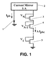
- Figure 1 shows the most basic embodiment of the circuit, object of the invention.
- Said particular embodiment comprises a photodiode (1), which generates a photocurrent I ph , which is amplified by means of a current mirror (2) having a gain A.
- the amplified current leads to a chain of N transistors (3, 4 and 5), N being a natural number, all of which have connected their gate to their drain, which is known by connection in diode configuration.
- Figure 1 shows 3 transistors, which may in reality be any number N of transistors.
- the parameters A corresponding to the gain of the current mirror and I g corresponding to a parameter characteristic of the FET transistor, usually referred to as "specific current" undergo great variation from pixel to pixel, whilst U T is an equal physical constant for all the pixels.
- the parameter n corresponding to a further parameter characteristic of the FET transistor usually known as “gradient factor” undergoes a relatively low variation from pixel to pixel.
- this circuit adds the N factor (N being the number of transistors in each stage) to the gain obtained by means of previous techniques and the parameters which undergo great dispersions from pixel to pixel A and I g do not intervene.
- Figure 3 shows an exemplary embodiment with two stages, each one an additional gain "3". It shows a possible embodiment of the current mirrors.
- 3 FET transistors (3', 4' and 5') have been employed in cascade in each one of the steps.
- a FET transistor (11) is positioned at the input of the second stage with the source connected to a voltage V Q in order to generate the current I 2 .
- the current mirrors are basic circuits well known in literature on analog integrated circuit design. These copy the current in its input branch to the output branch, giving to said output branch an optional amplification or attenuation.
- the current mirror of the first stage is formed by three elements, two PMOS FET transistors (6, 7) being with their gate connected to respective constant voltage V a and V b and a voltage amplifier (8) with a gain which is high enough to generate the "virtual ground" conditions in the node that joins the photodiode (1) to the first PMOS transistor (6), thus improving the velocity of the circuit noticeably.
- the current mirror of the second stage (8, 9 and 10) is identical to that of the first stage, although it may be polarized with different voltages V c and V d , which would give rise to a different gain.
- each photodiode is required to capture light in each pixel. Therefore, in each pixel of the DVS camera, there would be a transimpedance stage (or stages in cascade).
- the input current may come from another circuit which is not a photodiode.
Landscapes
- Engineering & Computer Science (AREA)
- Power Engineering (AREA)
- Multimedia (AREA)
- Signal Processing (AREA)
- Transforming Light Signals Into Electric Signals (AREA)
- Amplifiers (AREA)
- Studio Devices (AREA)
- Solid State Image Pick-Up Elements (AREA)
Abstract
Description
- The present invention, as expressed in the present descriptive specification, refers to a low-mismatch and low-consumption transimpedance gain circuit for temporally differentiating photo-sensing systems in dynamic vision sensors (DVS), by means of transistors connected in diode.
- The invention falls within the field of electronic circuits, especially low-consumption reduced-area analog integrated circuits. The circuit specifically pertains to the category of voltage current preamplifiers or in other words, transimpedance.
- Dynamic vision sensors (DVS) are new integrated circuits of the video camera variety, although they are not specifically such. In commercial video cameras, the apparatus records photogram after photogram. In DVS, there are no photograms. The integrated circuit contains a photo sensor matrix, similar to video cameras. In video cameras, each photo sensor is sampled with a fixed frequency. However, in DVS, the pixels are not sampled. Every pixel calculates the time derivative of the light it senses, and when this exceeds a certain level (threshold), the pixel emits an "event" outwards. The event usually consists of the (x,y) coordinate of the pixel within the two-dimensional photo sensor matrix. In this way, the output of a DVS consists of a flow of (x,y) coordinates of the various pixels that detect a change in the intensity they sense. This type of DVS sensor were reported for the first time by Lichtsteiner, Delbruck and Posch in 2006 ("A 128 x 128 120dB 30mW Asynchronous Vision Sensor that Responds to Relative Intensity Change" in Visuals Supplement to ISSCC Dig. Of Tech. Papers, San Fransisco, 2006, vol., pp 508-509 (27.9) and subsequently in more detail in P. Lichtsteiner, C. Posch and T. Delbruck, ("A 128 x128 120dB 15µs Latency Asynchronous Temporal Contrast Vision Sensor", IEEE J. Solid-State Circuits, vol. 43, No. 2, pp. 566-576, Feb. 2008).
- More recently, Posch has reported a new prototype (C. Posch, D. Matolin and R. Wohlgenannt, "A QGVA 143dB dynamic range asynchronous address-event PWM dynamic image sensor with lossless pixel level video-compression", Solid-State Circuits, 2010 IEEE International Conference ISSCC, Dig of Tech Paper, pp. 400-401, February 2010).
- However, in these DVS sensors, the photocurrent Iph sensed by a photo sensor is firstly transformed into voltage by means of a logarithmic conversion. This voltage is firstly amplified and its time derivative subsequently calculated. A crucial parameter is the voltage gain in this first amplification. The greater the amplification, the more sensitive the sensor will be to the "Temporal Contrast". The problem is that this amplification should be carried out within each pixel of the matrix and should be carried out by a circuit which consumes little power and little area in the microchip. Moreover, it is important that it is carried out by a circuit which does not undergo too much dispersion in the gain value from one pixel to another, given that in the contrary case, it would introduce much variation into the behaviour of the various pixels in comparison to one another, thereby reducing the overall sensitivity of the sensor. The DVS reported to date employ voltage amplification stages based on circuits with capacitors. In integrated analog circuits, the condensers have low-dispersion between one another and are therefore highly suitable for carrying out voltage amplification stages. However, in DVS, obtaining voltage gains of around 20 to 100 (or over) is desirable. Upon doing so with condensers, at least two condensers are required, the value proportion of which is equal to that of the desired gain. Given that the area of the condensers is proportional to their value this means that one of the condensers should have an area which is between 20 and 100 times greater than the other. The end result is that a large part of the area of the pixel is consumed in the condensers.
- A possible alternative may be to obtain the voltage gain by means of two consecutive stages, given that the gain of each stage is multiplied. However, the synchronisation required between the two consecutive stages also makes it too long, thus reducing the speed of the DVS dramatically.
- In order to achieve the objectives and avoid the limitations set out above, the present invention consists of a low-mismatch and low-consumption transimpedance gain circuit for temporally differentiating photo-sensing systems in dynamic vision sensors (DVS), by means of transistors connected in diode.
- Therefore, the present invention refers to a low-mismatch and low-consumption transimpedance gain circuit for temporally differentiating photo-sensing systems in dynamic vision sensors (DVS), which employs at least one photodiode, the system being characterised in that it comprises at least two in-series transistors, each one of the transistors being connected in diode configuration and being positioned at the output of the photodiode, the output current of the photodiode flowing through the drain-source channels of the transistors and the source of the last in-series transistor being connected to a voltage selected from an ground voltage, a constant voltage and a controlled voltage. Therefore, the pixels of the cameras which make use of dynamic vision sensors, also known as DVS cameras, need at least one photosensor to generate the input current to the transimpedance circuit. However, if said circuit is used in another context, the input current may come from another circuit or element which is not a photodiode. In fact, when several of these stages are used in cascade, for example, only the first one receives the current from the photodiode; the rest receive it from a transistor.
- In a preferred embodiment of the invention, the at least two transistors have a exponential voltage-current characteristic.
- In another preferred embodiment of the invention, the transistors are of the FET (field-effect transistor) variety, being polarised in weak inversion.
- In a further preferred embodiment of the invention, the circuit comprises a number of means for controlling the polarity of the electrical current generated in the photodiode, the means for controlling the polarity are positioned between the photodiode and the at least two transistors. These means for controlling the polarity are optional and improve the output of the circuit by obtaining a faster circuit response.
- In an additional embodiment of the invention, the means for controlling the polarity comprise electrical current copying and inversion means.
- In another preferred embodiment of the invention, the means for controlling polarity comprise electrical current amplification means.
- In an additional further embodiment of the invention, the means for controlling the polarity are a current mirror in series with the photodiode, the output current of the means for controlling the polarity constituting that which flows through the drain-source channels of the at least two transistors.
- In another preferred embodiment of the invention, the circuit comprises a circuit for automatically controlling the gain of the current mirror between the current mirror and the at least two transistors.
- In a further preferred embodiment of the invention, the current comprises having logarithmic dependence between the output voltage, in comparison to the current generated by the photodiode.
- In addition, the present invention considers the use of the low-mismatch and low-consumption transimpedance gain circuit for temporally differentiating photo-sensing systems in DVS for generating a voltage amplification stage by means of positioning said transimpedance gain circuit as a stage prior to a transconductance circuit.
- The present invention also comprises the use of the low-mismatch and low-consumption transimpedance gain circuit for temporally differentiating photo-sensing systems in DVS to generate a voltage amplification stage by means of positioning the transimpedance gain circuit as a stage subsequent to a transconductance circuit.
- Furthermore, the present invention also comprises the use of the low-mismatch and low-consumption transimpedance gain circuit for temporarily differentiating photo-sensing systems in DVS as a stage prior to a signal branch circuit for sending the signal to the output which eliminates the continuous voltage of the output signal of the transimpedance gain circuit, thereby reducing dispersions between all of the pixels.
-
- Figure 1 is an example of an embodiment of the present invention, comprising one single stage.
- Figure 2 is an example of an embodiment of the invention, wherein the circuit is composed of two stages.
- Figure 3 is an example of an embodiment in the circuit, wherein the circuit comprises having two stages, each one of which has a gain equal to "3".
- Below is an illustrative and non-limiting description of various particular embodiments of the invention, making reference to the numbering adopted in the figures.
- In the present invention, the circuit that transforms the photocurrent to a voltage, by means of a logarithmic conversion, carries out, implicitly, a voltage amplification with low dispersion of the gain between the various pixels within the same microchip.
- Therefore,
Figure 1 shows the most basic embodiment of the circuit, object of the invention. Said particular embodiment comprises a photodiode (1), which generates a photocurrent Iph, which is amplified by means of a current mirror (2) having a gain A. The amplified current leads to a chain of N transistors (3, 4 and 5), N being a natural number, all of which have connected their gate to their drain, which is known by connection in diode configuration. Please note thatFigure 1 shows 3 transistors, which may in reality be any number N of transistors. - In the event of an embodiment with NMOS FET transistors, the voltage difference formed in each transistor (3, 4 and 5), polarised in weak inversion, is approximately the same and equals

- In this way, the voltage obtained in the highest transistor is approximately

- In an embodiment of the integrated circuit, the parameters A, corresponding to the gain of the current mirror and Ig corresponding to a parameter characteristic of the FET transistor, usually referred to as "specific current", undergo great variation from pixel to pixel, whilst UT is an equal physical constant for all the pixels. The parameter n, corresponding to a further parameter characteristic of the FET transistor usually known as "gradient factor" undergoes a relatively low variation from pixel to pixel. When the output voltage V N is taken to the branched circuit, it provides the output

- In such a way that this circuit adds the N factor (N being the number of transistors in each stage) to the gain obtained by means of previous techniques and the parameters which undergo great dispersions from pixel to pixel A and Ig do not intervene.
- In practice it is not possible to use very high N values, being limited to 3 or 4. However, it is possible to connect different stages in cascade, like those shown in
Figure 1 . This is shown inFigure 2 , where the first stage has N 1 in-series transistors and the second stage has N 2. - The voltage formed in the first block VN1 (3) is carried to the gate of a transistor (11) with the source connected to VQ , generating a
current 
- Upon deriving the output from the circuit VN1, the following approximate result is obtained:

- Once again, the parameters of high dispersion index between pixels do not appear in the final equation. This method makes it possible to expand to more successive stages.
-
Figure 3 shows an exemplary embodiment with two stages, each one an additional gain "3". It shows a possible embodiment of the current mirrors. In order to achieve said additional gain, 3 FET transistors (3', 4' and 5') have been employed in cascade in each one of the steps. A FET transistor (11) is positioned at the input of the second stage with the source connected to a voltage VQ in order to generate the current I2 . - The current mirrors are basic circuits well known in literature on analog integrated circuit design. These copy the current in its input branch to the output branch, giving to said output branch an optional amplification or attenuation. In
Figure 3 , the current mirror of the first stage is formed by three elements, two PMOS FET transistors (6, 7) being with their gate connected to respective constant voltage Va and Vb and a voltage amplifier (8) with a gain which is high enough to generate the "virtual ground" conditions in the node that joins the photodiode (1) to the first PMOS transistor (6), thus improving the velocity of the circuit noticeably. The current mirror of the second stage (8, 9 and 10) is identical to that of the first stage, although it may be polarized with different voltages Vc and Vd , which would give rise to a different gain. - These circuits, which are repeated for each pixel, should be complemented by a number of polarisation circuits, shared between all the pixels, in order to fix the voltages Va, Vb, Vc, Vd and VQ.
- In the specific case of using DVS cameras, at least one photodiode is required to capture light in each pixel. Therefore, in each pixel of the DVS camera, there would be a transimpedance stage (or stages in cascade).
- If the stage is used in a context other than that of the DVS cameras, the input current may come from another circuit which is not a photodiode. In fact, for example, when several of these stages are used in cascade, only the first receives the current from the diode. The rest receive it from a transistor.
Claims (12)
- Low-mismatch and low-consumption transimpedance gain circuit for temporally differentiating photo-sensing systems in dynamic vision sensors, which employs at least one photodiode, wherein the system comprises at least two in-series transistors, each one of the transistors being connected in diode configuration and being positioned at the output of the photodiode, the output current of the photodiode flowing through the drain-source channels of the transistors and the last in-series transistor having the source connected to a voltage selected between an ground voltage, a constant voltage and a controlled voltage.
- Transimpedance gain circuit according to claim 1, wherein the at least two transistors have an exponential type current-voltage characteristic.
- Transimpedance gain circuit according to claim 2, wherein when the transistors are FET transistors and they are polarized in weak inversion.
- Transimpedance gain circuit according to claim 1, wherein it comprises means for controlling polarity of the electrical current generated in the photodiode, the means for controlling the polarity being positioned between the at least one photodiode and the at least two transistors.
- Transimpedance gain circuit according to claim 4, wherein the means for controlling the polarity comprise electric current copying and inversion means.
- Transimpedance gain circuit according to claim 5, wherein the means for controlling the polarity comprise electric current amplification mean.
- Transimpedance gain circuit according to claim 5 or 6, wherein the means for controlling the polarity are a current mirror in series with the photodiode, the output current of the means for controlling the polarity being that which flows through the drain-source channels of the at least two transistors.
- Transimpedance gain circuit according to claim 7, wherein it comprises a circuit for automatically controlling the gain of the current mirror placed between the current mirror and the at least two transistors.
- Transimpedance gain circuit according to any of the previous claims, wherein it comprises having a logarithmic dependence between the output voltage versus the current generated by the photodiode.
- Use of the transimpedance gain circuit defined in claims 1 to 9 for generating a current amplification stage by means of positioning the transimpedance gain circuit as a stage prior to a transconductance circuit.
- Use of the transimpedance gain circuit defined in claims 1 to 9 for generating a voltage amplification stage by means of positioning the transimpedance gain circuit as a stage subsequent to a transconductance circuit.
- Use of the transimpedance gain circuit defined in claims 1 to 9 to be employed as a stage prior to a branch circuit for the signal at the output which eliminates the continuous voltage of the output signal of the transimpedance gain circuit, thereby reducing dispersions among the pixels.
Applications Claiming Priority (2)
| Application Number | Priority Date | Filing Date | Title |
|---|---|---|---|
| ES201130862A ES2396816B1 (en) | 2011-05-26 | 2011-05-26 | LOW CONSUMPTION AND LOW DISAPPEARANCE TRANSIMPEDANCE GAIN CIRCUIT FOR TEMPORARY DIFFERENTIAL PHOTOSENSING SYSTEMS IN VISION DYNAMIC SENSORS |
| PCT/ES2012/070363 WO2012160230A1 (en) | 2011-05-26 | 2012-05-22 | Low-mismatch and low-consumption transimpedance gain circuit for temporally differentiating photo-sensing systems in dynamic vision sensors |
Publications (3)
| Publication Number | Publication Date |
|---|---|
| EP2717466A1 true EP2717466A1 (en) | 2014-04-09 |
| EP2717466A4 EP2717466A4 (en) | 2014-10-15 |
| EP2717466B1 EP2717466B1 (en) | 2016-08-10 |
Family
ID=47216645
Family Applications (1)
| Application Number | Title | Priority Date | Filing Date |
|---|---|---|---|
| EP12789077.0A Active EP2717466B1 (en) | 2011-05-26 | 2012-05-22 | Low-mismatch and low-consumption transimpedance gain circuit for temporally differentiating photo-sensing systems in dynamic vision sensors |
Country Status (7)
| Country | Link |
|---|---|
| US (1) | US9681081B2 (en) |
| EP (1) | EP2717466B1 (en) |
| JP (1) | JP5922226B2 (en) |
| KR (1) | KR101885093B1 (en) |
| CN (1) | CN103875180B (en) |
| ES (2) | ES2396816B1 (en) |
| WO (1) | WO2012160230A1 (en) |
Cited By (3)
| Publication number | Priority date | Publication date | Assignee | Title |
|---|---|---|---|---|
| WO2017174579A1 (en) * | 2016-04-04 | 2017-10-12 | Chronocam | Sample and hold based temporal contrast vision sensor |
| US10401217B2 (en) | 2016-08-30 | 2019-09-03 | Samsung Electronics Co., Ltd. | Data output device |
| WO2021198498A1 (en) * | 2020-04-02 | 2021-10-07 | Prophesee | Pixel circuit and method for vision sensor |
Families Citing this family (12)
| Publication number | Priority date | Publication date | Assignee | Title |
|---|---|---|---|---|
| JP2991747B2 (en) | 1990-07-06 | 1999-12-20 | 松下電器産業株式会社 | Electrophotographic equipment |
| ES2476115B1 (en) * | 2012-12-11 | 2015-04-20 | Consejo Superior De Investigaciones Científicas (Csic) | METHOD AND DEVICE FOR THE DETECTION OF THE TEMPORARY VARIATION OF LIGHT INTENSITY IN A PHOTOSENSOR MATRIX |
| CN104956654B (en) * | 2013-11-12 | 2018-09-18 | 康斯乔最高科学研究公司 | Method and apparatus for detecting the light intensity time-varying in photosensor matrix |
| US10043064B2 (en) | 2015-01-14 | 2018-08-07 | Samsung Electronics Co., Ltd. | Method and apparatus of detecting object using event-based sensor |
| KR102426677B1 (en) | 2015-03-09 | 2022-07-28 | 삼성전자주식회사 | Vision sensor based on event and difference amplifier with reduced noise and offset |
| US9755760B2 (en) * | 2015-10-05 | 2017-09-05 | Avago Technologies General Ip (Singapore) Pte. Ltd. | Supply voltage modular photodiode bias |
| KR102421141B1 (en) | 2015-10-30 | 2022-07-14 | 삼성전자주식회사 | Apparatus and method for storing event signal and image and operating method of vision sensor for transmitting event signal to the apparatus |
| EP3313064A1 (en) * | 2016-10-20 | 2018-04-25 | Chronocam | Pixel circuit for detecting time-dependent visual data |
| KR102707749B1 (en) | 2019-03-28 | 2024-09-23 | 삼성전자주식회사 | Dynamic vision sensor configured to calibrate event signals using optical black region and method of operating the same |
| KR102742056B1 (en) | 2020-02-10 | 2024-12-16 | 삼성전자주식회사 | Dynamic vision sensor device including buffer |
| KR102885924B1 (en) | 2021-05-18 | 2025-11-12 | 삼성전자주식회사 | Vision sensor, and operating method thereof |
| KR20240151414A (en) | 2023-04-11 | 2024-10-18 | 삼성전자주식회사 | Stacked hybrid dynamic vision sensor for low light environment and the operating method therofimage sensor with junctionless transfer transistor |
Family Cites Families (18)
| Publication number | Priority date | Publication date | Assignee | Title |
|---|---|---|---|---|
| US3638050A (en) * | 1970-04-01 | 1972-01-25 | Texas Instruments Inc | Preamplification circuitry for photoconductive sensors |
| US5155353A (en) * | 1991-08-14 | 1992-10-13 | Tandberg Data | High dynamic range integrated opto-electronic sensor and MOSFET amplifiers for pulsed light |
| US5508836A (en) * | 1994-09-13 | 1996-04-16 | Irvine Sensors Corporation | Infrared wireless communication between electronic system components |
| JPH08265068A (en) * | 1995-03-10 | 1996-10-11 | At & T Corp | Gain control circuit |
| CA2198161A1 (en) | 1996-02-23 | 1997-08-24 | Naoki Nishiyama | Preamplifier for optical communication |
| US6194695B1 (en) | 1998-08-27 | 2001-02-27 | The United States Of America As Represented By The Secretary Of The Navy | Photoreceptor array for linear optical flow measurement |
| KR100630083B1 (en) | 2002-04-26 | 2006-09-27 | 삼성전자주식회사 | Automatic Gain Control Device for Burst Mode Optical Receiver |
| ITUD20020139A1 (en) * | 2002-06-19 | 2003-12-19 | Neuricam Spa | PHOTOSENSITIVE ELEMENT FOR ELECTRO-OPTICAL SENSORS |
| US7259363B2 (en) * | 2003-01-14 | 2007-08-21 | Koninklijke Philips Electronics N.V. | Circuit arrangement and methods for a remote control receiver having a photodiode |
| JP3691050B2 (en) * | 2003-10-30 | 2005-08-31 | 総吉 廣津 | Semiconductor image sensor |
| US7265631B2 (en) | 2005-03-12 | 2007-09-04 | Avago Technologies Ecbu Ip (Singapore) Pte. Ltd. | Transimpedance amplifier with signal amplification circuit that performs power signal regulation |
| JP5244587B2 (en) | 2005-06-03 | 2013-07-24 | ウニヴェルズィテート チューリッヒ | Photoarray for detecting time-dependent image data |
| AT504582B1 (en) | 2006-11-23 | 2008-12-15 | Arc Austrian Res Centers Gmbh | METHOD FOR GENERATING AN IMAGE IN ELECTRONIC FORM, PICTURE ELEMENT FOR AN IMAGE SENSOR FOR GENERATING AN IMAGE AND PICTOR SENSOR |
| US7554073B2 (en) * | 2007-01-22 | 2009-06-30 | Avago Technologies Ecbu Ip (Singapore) Pte. Ltd. | High linearity CMOS ambient light sensor |
| WO2008123119A1 (en) * | 2007-03-26 | 2008-10-16 | Semiconductor Energy Laboratory Co., Ltd. | Photoelectric conversion device and electronic device provided with the photoelectric conversion device |
| JP5304642B2 (en) | 2007-03-29 | 2013-10-02 | 日本電気株式会社 | Signal amplifier for optical receiver circuit |
| KR101401528B1 (en) * | 2007-06-29 | 2014-06-03 | 가부시키가이샤 한도오따이 에네루기 켄큐쇼 | Photoelectric conversion device and electronic device provided with the photoelectric conversion device |
| EP2026479A1 (en) * | 2007-08-17 | 2009-02-18 | Leica Geosystems AG | Transimpedance amplifier switch for a photo detector |
-
2011
- 2011-05-26 ES ES201130862A patent/ES2396816B1/en not_active Expired - Fee Related
-
2012
- 2012-05-22 EP EP12789077.0A patent/EP2717466B1/en active Active
- 2012-05-22 US US14/119,942 patent/US9681081B2/en not_active Expired - Fee Related
- 2012-05-22 CN CN201280036724.0A patent/CN103875180B/en not_active Expired - Fee Related
- 2012-05-22 WO PCT/ES2012/070363 patent/WO2012160230A1/en not_active Ceased
- 2012-05-22 KR KR1020137034589A patent/KR101885093B1/en not_active Expired - Fee Related
- 2012-05-22 JP JP2014511916A patent/JP5922226B2/en not_active Expired - Fee Related
- 2012-05-22 ES ES12789077.0T patent/ES2592652T3/en active Active
Cited By (9)
| Publication number | Priority date | Publication date | Assignee | Title |
|---|---|---|---|---|
| WO2017174579A1 (en) * | 2016-04-04 | 2017-10-12 | Chronocam | Sample and hold based temporal contrast vision sensor |
| US10469776B2 (en) | 2016-04-04 | 2019-11-05 | Prophesee | Sample and hold based temporal contrast vision sensor |
| US10904465B2 (en) | 2016-04-04 | 2021-01-26 | Prophesee | Sample and hold based temporal contrast vision sensor |
| US10401217B2 (en) | 2016-08-30 | 2019-09-03 | Samsung Electronics Co., Ltd. | Data output device |
| US11125615B2 (en) | 2016-08-30 | 2021-09-21 | Samsung Electronics Co., Ltd. | Data output device |
| US11604092B2 (en) | 2016-08-30 | 2023-03-14 | Samsung Electronics Co., Ltd. | Data output device |
| US12061115B2 (en) | 2016-08-30 | 2024-08-13 | Samsung Electronics Co., Ltd. | Data output device |
| WO2021198498A1 (en) * | 2020-04-02 | 2021-10-07 | Prophesee | Pixel circuit and method for vision sensor |
| US11885673B2 (en) | 2020-04-02 | 2024-01-30 | Prophesee | Pixel circuit including an open-loop amplifier with well controlled gain for event-based vision sensor and method of controlling thereof |
Also Published As
| Publication number | Publication date |
|---|---|
| KR101885093B1 (en) | 2018-08-03 |
| ES2592652T3 (en) | 2016-11-30 |
| ES2396816A1 (en) | 2013-02-27 |
| CN103875180B (en) | 2017-07-18 |
| EP2717466A4 (en) | 2014-10-15 |
| JP2014515577A (en) | 2014-06-30 |
| EP2717466B1 (en) | 2016-08-10 |
| KR20140053030A (en) | 2014-05-07 |
| WO2012160230A1 (en) | 2012-11-29 |
| US9681081B2 (en) | 2017-06-13 |
| JP5922226B2 (en) | 2016-05-24 |
| CN103875180A (en) | 2014-06-18 |
| US20140231623A1 (en) | 2014-08-21 |
| ES2396816B1 (en) | 2014-01-21 |
Similar Documents
| Publication | Publication Date | Title |
|---|---|---|
| EP2717466B1 (en) | Low-mismatch and low-consumption transimpedance gain circuit for temporally differentiating photo-sensing systems in dynamic vision sensors | |
| EP3440833B1 (en) | Sample and hold based temporal contrast vision sensor | |
| US12061115B2 (en) | Data output device | |
| US8183513B2 (en) | In-cell current subtraction for infrared detectors | |
| JP2016533140A (en) | Dynamic, single photodiode pixel circuit and method of operation thereof | |
| US20170255860A1 (en) | Methods and systems of neuron leaky integrate and fire circuits | |
| CN104956654A (en) | Method and device for detecting the temporal variation of the light intensity in a matrix of photosensors | |
| US8629726B1 (en) | High-performance amplifier for transducer array input unit cell | |
| JP5264418B2 (en) | Thermal infrared detector | |
| US4728828A (en) | Switched capacitor transresistance amplifier | |
| CN118118810A (en) | Dynamic vision sensor and event detection method | |
| JPH0732261B2 (en) | Semiconductor light receiving device | |
| US9063013B2 (en) | Infrared detector | |
| EP3079355B1 (en) | Dual-mode photosensitive pixel with gain stage | |
| RU2710298C1 (en) | Non-inverting amplifier with current output for operation at low temperatures | |
| JP4359686B2 (en) | Avalanche photodiode (APD) multiplication factor detection circuit | |
| HK40008064A (en) | Sample and hold based temporal contrast vision sensor | |
| JPS59100641A (en) | Agc system of average optical power detection |
Legal Events
| Date | Code | Title | Description |
|---|---|---|---|
| PUAI | Public reference made under article 153(3) epc to a published international application that has entered the european phase |
Free format text: ORIGINAL CODE: 0009012 |
|
| 17P | Request for examination filed |
Effective date: 20131223 |
|
| AK | Designated contracting states |
Kind code of ref document: A1 Designated state(s): AL AT BE BG CH CY CZ DE DK EE ES FI FR GB GR HR HU IE IS IT LI LT LU LV MC MK MT NL NO PL PT RO RS SE SI SK SM TR |
|
| DAX | Request for extension of the european patent (deleted) | ||
| A4 | Supplementary search report drawn up and despatched |
Effective date: 20140911 |
|
| RIC1 | Information provided on ipc code assigned before grant |
Ipc: H03F 3/345 20060101ALI20140905BHEP Ipc: H03F 1/08 20060101ALI20140905BHEP Ipc: H03F 3/08 20060101AFI20140905BHEP Ipc: H04N 5/378 20110101ALI20140905BHEP |
|
| 17Q | First examination report despatched |
Effective date: 20150715 |
|
| GRAP | Despatch of communication of intention to grant a patent |
Free format text: ORIGINAL CODE: EPIDOSNIGR1 |
|
| INTG | Intention to grant announced |
Effective date: 20160510 |
|
| GRAS | Grant fee paid |
Free format text: ORIGINAL CODE: EPIDOSNIGR3 |
|
| GRAA | (expected) grant |
Free format text: ORIGINAL CODE: 0009210 |
|
| AK | Designated contracting states |
Kind code of ref document: B1 Designated state(s): AL AT BE BG CH CY CZ DE DK EE ES FI FR GB GR HR HU IE IS IT LI LT LU LV MC MK MT NL NO PL PT RO RS SE SI SK SM TR |
|
| REG | Reference to a national code |
Ref country code: GB Ref legal event code: FG4D |
|
| REG | Reference to a national code |
Ref country code: CH Ref legal event code: EP Ref country code: AT Ref legal event code: REF Ref document number: 819845 Country of ref document: AT Kind code of ref document: T Effective date: 20160815 |
|
| REG | Reference to a national code |
Ref country code: IE Ref legal event code: FG4D |
|
| REG | Reference to a national code |
Ref country code: DE Ref legal event code: R096 Ref document number: 602012021573 Country of ref document: DE |
|
| REG | Reference to a national code |
Ref country code: CH Ref legal event code: NV Representative=s name: ISLER AND PEDRAZZINI AG, CH |
|
| REG | Reference to a national code |
Ref country code: ES Ref legal event code: FG2A Ref document number: 2592652 Country of ref document: ES Kind code of ref document: T3 Effective date: 20161130 |
|
| REG | Reference to a national code |
Ref country code: LT Ref legal event code: MG4D |
|
| REG | Reference to a national code |
Ref country code: NL Ref legal event code: MP Effective date: 20160810 |
|
| PG25 | Lapsed in a contracting state [announced via postgrant information from national office to epo] |
Ref country code: FI Free format text: LAPSE BECAUSE OF FAILURE TO SUBMIT A TRANSLATION OF THE DESCRIPTION OR TO PAY THE FEE WITHIN THE PRESCRIBED TIME-LIMIT Effective date: 20160810 Ref country code: IS Free format text: LAPSE BECAUSE OF FAILURE TO SUBMIT A TRANSLATION OF THE DESCRIPTION OR TO PAY THE FEE WITHIN THE PRESCRIBED TIME-LIMIT Effective date: 20161210 Ref country code: NL Free format text: LAPSE BECAUSE OF FAILURE TO SUBMIT A TRANSLATION OF THE DESCRIPTION OR TO PAY THE FEE WITHIN THE PRESCRIBED TIME-LIMIT Effective date: 20160810 Ref country code: RS Free format text: LAPSE BECAUSE OF FAILURE TO SUBMIT A TRANSLATION OF THE DESCRIPTION OR TO PAY THE FEE WITHIN THE PRESCRIBED TIME-LIMIT Effective date: 20160810 Ref country code: LT Free format text: LAPSE BECAUSE OF FAILURE TO SUBMIT A TRANSLATION OF THE DESCRIPTION OR TO PAY THE FEE WITHIN THE PRESCRIBED TIME-LIMIT Effective date: 20160810 Ref country code: HR Free format text: LAPSE BECAUSE OF FAILURE TO SUBMIT A TRANSLATION OF THE DESCRIPTION OR TO PAY THE FEE WITHIN THE PRESCRIBED TIME-LIMIT Effective date: 20160810 Ref country code: NO Free format text: LAPSE BECAUSE OF FAILURE TO SUBMIT A TRANSLATION OF THE DESCRIPTION OR TO PAY THE FEE WITHIN THE PRESCRIBED TIME-LIMIT Effective date: 20161110 |
|
| PG25 | Lapsed in a contracting state [announced via postgrant information from national office to epo] |
Ref country code: GR Free format text: LAPSE BECAUSE OF FAILURE TO SUBMIT A TRANSLATION OF THE DESCRIPTION OR TO PAY THE FEE WITHIN THE PRESCRIBED TIME-LIMIT Effective date: 20161111 Ref country code: PT Free format text: LAPSE BECAUSE OF FAILURE TO SUBMIT A TRANSLATION OF THE DESCRIPTION OR TO PAY THE FEE WITHIN THE PRESCRIBED TIME-LIMIT Effective date: 20161212 Ref country code: PL Free format text: LAPSE BECAUSE OF FAILURE TO SUBMIT A TRANSLATION OF THE DESCRIPTION OR TO PAY THE FEE WITHIN THE PRESCRIBED TIME-LIMIT Effective date: 20160810 Ref country code: LV Free format text: LAPSE BECAUSE OF FAILURE TO SUBMIT A TRANSLATION OF THE DESCRIPTION OR TO PAY THE FEE WITHIN THE PRESCRIBED TIME-LIMIT Effective date: 20160810 Ref country code: SE Free format text: LAPSE BECAUSE OF FAILURE TO SUBMIT A TRANSLATION OF THE DESCRIPTION OR TO PAY THE FEE WITHIN THE PRESCRIBED TIME-LIMIT Effective date: 20160810 |
|
| REG | Reference to a national code |
Ref country code: FR Ref legal event code: PLFP Year of fee payment: 6 |
|
| PG25 | Lapsed in a contracting state [announced via postgrant information from national office to epo] |
Ref country code: RO Free format text: LAPSE BECAUSE OF FAILURE TO SUBMIT A TRANSLATION OF THE DESCRIPTION OR TO PAY THE FEE WITHIN THE PRESCRIBED TIME-LIMIT Effective date: 20160810 Ref country code: EE Free format text: LAPSE BECAUSE OF FAILURE TO SUBMIT A TRANSLATION OF THE DESCRIPTION OR TO PAY THE FEE WITHIN THE PRESCRIBED TIME-LIMIT Effective date: 20160810 |
|
| REG | Reference to a national code |
Ref country code: DE Ref legal event code: R097 Ref document number: 602012021573 Country of ref document: DE |
|
| PG25 | Lapsed in a contracting state [announced via postgrant information from national office to epo] |
Ref country code: BG Free format text: LAPSE BECAUSE OF FAILURE TO SUBMIT A TRANSLATION OF THE DESCRIPTION OR TO PAY THE FEE WITHIN THE PRESCRIBED TIME-LIMIT Effective date: 20161110 Ref country code: SK Free format text: LAPSE BECAUSE OF FAILURE TO SUBMIT A TRANSLATION OF THE DESCRIPTION OR TO PAY THE FEE WITHIN THE PRESCRIBED TIME-LIMIT Effective date: 20160810 Ref country code: DK Free format text: LAPSE BECAUSE OF FAILURE TO SUBMIT A TRANSLATION OF THE DESCRIPTION OR TO PAY THE FEE WITHIN THE PRESCRIBED TIME-LIMIT Effective date: 20160810 Ref country code: SM Free format text: LAPSE BECAUSE OF FAILURE TO SUBMIT A TRANSLATION OF THE DESCRIPTION OR TO PAY THE FEE WITHIN THE PRESCRIBED TIME-LIMIT Effective date: 20160810 Ref country code: BE Free format text: LAPSE BECAUSE OF FAILURE TO SUBMIT A TRANSLATION OF THE DESCRIPTION OR TO PAY THE FEE WITHIN THE PRESCRIBED TIME-LIMIT Effective date: 20160810 Ref country code: CZ Free format text: LAPSE BECAUSE OF FAILURE TO SUBMIT A TRANSLATION OF THE DESCRIPTION OR TO PAY THE FEE WITHIN THE PRESCRIBED TIME-LIMIT Effective date: 20160810 |
|
| PLBE | No opposition filed within time limit |
Free format text: ORIGINAL CODE: 0009261 |
|
| STAA | Information on the status of an ep patent application or granted ep patent |
Free format text: STATUS: NO OPPOSITION FILED WITHIN TIME LIMIT |
|
| 26N | No opposition filed |
Effective date: 20170511 |
|
| PG25 | Lapsed in a contracting state [announced via postgrant information from national office to epo] |
Ref country code: SI Free format text: LAPSE BECAUSE OF FAILURE TO SUBMIT A TRANSLATION OF THE DESCRIPTION OR TO PAY THE FEE WITHIN THE PRESCRIBED TIME-LIMIT Effective date: 20160810 Ref country code: LU Free format text: LAPSE BECAUSE OF NON-PAYMENT OF DUE FEES Effective date: 20170531 |
|
| PG25 | Lapsed in a contracting state [announced via postgrant information from national office to epo] |
Ref country code: MC Free format text: LAPSE BECAUSE OF FAILURE TO SUBMIT A TRANSLATION OF THE DESCRIPTION OR TO PAY THE FEE WITHIN THE PRESCRIBED TIME-LIMIT Effective date: 20160810 |
|
| REG | Reference to a national code |
Ref country code: IE Ref legal event code: MM4A |
|
| REG | Reference to a national code |
Ref country code: FR Ref legal event code: PLFP Year of fee payment: 7 |
|
| PG25 | Lapsed in a contracting state [announced via postgrant information from national office to epo] |
Ref country code: LU Free format text: LAPSE BECAUSE OF NON-PAYMENT OF DUE FEES Effective date: 20170522 |
|
| PG25 | Lapsed in a contracting state [announced via postgrant information from national office to epo] |
Ref country code: IE Free format text: LAPSE BECAUSE OF NON-PAYMENT OF DUE FEES Effective date: 20170522 |
|
| PG25 | Lapsed in a contracting state [announced via postgrant information from national office to epo] |
Ref country code: MT Free format text: LAPSE BECAUSE OF NON-PAYMENT OF DUE FEES Effective date: 20170522 |
|
| REG | Reference to a national code |
Ref country code: AT Ref legal event code: UEP Ref document number: 819845 Country of ref document: AT Kind code of ref document: T Effective date: 20160810 |
|
| PG25 | Lapsed in a contracting state [announced via postgrant information from national office to epo] |
Ref country code: AL Free format text: LAPSE BECAUSE OF FAILURE TO SUBMIT A TRANSLATION OF THE DESCRIPTION OR TO PAY THE FEE WITHIN THE PRESCRIBED TIME-LIMIT Effective date: 20160810 |
|
| PG25 | Lapsed in a contracting state [announced via postgrant information from national office to epo] |
Ref country code: HU Free format text: LAPSE BECAUSE OF FAILURE TO SUBMIT A TRANSLATION OF THE DESCRIPTION OR TO PAY THE FEE WITHIN THE PRESCRIBED TIME-LIMIT; INVALID AB INITIO Effective date: 20120522 |
|
| PG25 | Lapsed in a contracting state [announced via postgrant information from national office to epo] |
Ref country code: CY Free format text: LAPSE BECAUSE OF NON-PAYMENT OF DUE FEES Effective date: 20160810 |
|
| PG25 | Lapsed in a contracting state [announced via postgrant information from national office to epo] |
Ref country code: MK Free format text: LAPSE BECAUSE OF FAILURE TO SUBMIT A TRANSLATION OF THE DESCRIPTION OR TO PAY THE FEE WITHIN THE PRESCRIBED TIME-LIMIT Effective date: 20160810 |
|
| PG25 | Lapsed in a contracting state [announced via postgrant information from national office to epo] |
Ref country code: TR Free format text: LAPSE BECAUSE OF FAILURE TO SUBMIT A TRANSLATION OF THE DESCRIPTION OR TO PAY THE FEE WITHIN THE PRESCRIBED TIME-LIMIT Effective date: 20160810 |
|
| PGFP | Annual fee paid to national office [announced via postgrant information from national office to epo] |
Ref country code: IT Payment date: 20200513 Year of fee payment: 9 |
|
| PGFP | Annual fee paid to national office [announced via postgrant information from national office to epo] |
Ref country code: AT Payment date: 20200511 Year of fee payment: 9 |
|
| PGFP | Annual fee paid to national office [announced via postgrant information from national office to epo] |
Ref country code: ES Payment date: 20210601 Year of fee payment: 10 |
|
| REG | Reference to a national code |
Ref country code: AT Ref legal event code: MM01 Ref document number: 819845 Country of ref document: AT Kind code of ref document: T Effective date: 20210522 |
|
| PG25 | Lapsed in a contracting state [announced via postgrant information from national office to epo] |
Ref country code: AT Free format text: LAPSE BECAUSE OF NON-PAYMENT OF DUE FEES Effective date: 20210522 |
|
| PG25 | Lapsed in a contracting state [announced via postgrant information from national office to epo] |
Ref country code: IT Free format text: LAPSE BECAUSE OF NON-PAYMENT OF DUE FEES Effective date: 20200522 |
|
| REG | Reference to a national code |
Ref country code: ES Ref legal event code: FD2A Effective date: 20230728 |
|
| PG25 | Lapsed in a contracting state [announced via postgrant information from national office to epo] |
Ref country code: ES Free format text: LAPSE BECAUSE OF NON-PAYMENT OF DUE FEES Effective date: 20220523 |
|
| PGFP | Annual fee paid to national office [announced via postgrant information from national office to epo] |
Ref country code: GB Payment date: 20240418 Year of fee payment: 13 |
|
| PGFP | Annual fee paid to national office [announced via postgrant information from national office to epo] |
Ref country code: DE Payment date: 20240418 Year of fee payment: 13 |
|
| PGFP | Annual fee paid to national office [announced via postgrant information from national office to epo] |
Ref country code: CH Payment date: 20240602 Year of fee payment: 13 |
|
| PGFP | Annual fee paid to national office [announced via postgrant information from national office to epo] |
Ref country code: FR Payment date: 20240521 Year of fee payment: 13 |
|
| PG25 | Lapsed in a contracting state [announced via postgrant information from national office to epo] |
Ref country code: IT Free format text: LAPSE BECAUSE OF NON-PAYMENT OF DUE FEES Effective date: 20210522 |
|
| REG | Reference to a national code |
Ref country code: DE Ref legal event code: R119 Ref document number: 602012021573 Country of ref document: DE |
|
| REG | Reference to a national code |
Ref country code: CH Ref legal event code: H13 Free format text: ST27 STATUS EVENT CODE: U-0-0-H10-H13 (AS PROVIDED BY THE NATIONAL OFFICE) Effective date: 20251223 |
|
| PG25 | Lapsed in a contracting state [announced via postgrant information from national office to epo] |
Ref country code: CH Free format text: LAPSE BECAUSE OF NON-PAYMENT OF DUE FEES Effective date: 20250531 |
|
| GBPC | Gb: european patent ceased through non-payment of renewal fee |
Effective date: 20250522 |
|
| PG25 | Lapsed in a contracting state [announced via postgrant information from national office to epo] |
Ref country code: GB Free format text: LAPSE BECAUSE OF NON-PAYMENT OF DUE FEES Effective date: 20250522 |
|
| PG25 | Lapsed in a contracting state [announced via postgrant information from national office to epo] |
Ref country code: DE Free format text: LAPSE BECAUSE OF NON-PAYMENT OF DUE FEES Effective date: 20251202 |
|
| PG25 | Lapsed in a contracting state [announced via postgrant information from national office to epo] |
Ref country code: FR Free format text: LAPSE BECAUSE OF NON-PAYMENT OF DUE FEES Effective date: 20250531 |