EP2717305A1 - Integrated circuit inspection device - Google Patents
Integrated circuit inspection device Download PDFInfo
- Publication number
- EP2717305A1 EP2717305A1 EP12793492.5A EP12793492A EP2717305A1 EP 2717305 A1 EP2717305 A1 EP 2717305A1 EP 12793492 A EP12793492 A EP 12793492A EP 2717305 A1 EP2717305 A1 EP 2717305A1
- Authority
- EP
- European Patent Office
- Prior art keywords
- light
- integrated circuit
- wavelength width
- irradiating
- wavelength
- Prior art date
- Legal status (The legal status is an assumption and is not a legal conclusion. Google has not performed a legal analysis and makes no representation as to the accuracy of the status listed.)
- Granted
Links
Images



Classifications
-
- G—PHYSICS
- G01—MEASURING; TESTING
- G01N—INVESTIGATING OR ANALYSING MATERIALS BY DETERMINING THEIR CHEMICAL OR PHYSICAL PROPERTIES
- G01N21/00—Investigating or analysing materials by the use of optical means, i.e. using sub-millimetre waves, infrared, visible or ultraviolet light
- G01N21/84—Systems specially adapted for particular applications
- G01N21/88—Investigating the presence of flaws or contamination
- G01N21/95—Investigating the presence of flaws or contamination characterised by the material or shape of the object to be examined
- G01N21/9501—Semiconductor wafers
-
- G—PHYSICS
- G01—MEASURING; TESTING
- G01N—INVESTIGATING OR ANALYSING MATERIALS BY DETERMINING THEIR CHEMICAL OR PHYSICAL PROPERTIES
- G01N21/00—Investigating or analysing materials by the use of optical means, i.e. using sub-millimetre waves, infrared, visible or ultraviolet light
- G01N21/17—Systems in which incident light is modified in accordance with the properties of the material investigated
- G01N21/55—Specular reflectivity
-
- G—PHYSICS
- G01—MEASURING; TESTING
- G01N—INVESTIGATING OR ANALYSING MATERIALS BY DETERMINING THEIR CHEMICAL OR PHYSICAL PROPERTIES
- G01N21/00—Investigating or analysing materials by the use of optical means, i.e. using sub-millimetre waves, infrared, visible or ultraviolet light
- G01N21/84—Systems specially adapted for particular applications
- G01N21/88—Investigating the presence of flaws or contamination
-
- G—PHYSICS
- G01—MEASURING; TESTING
- G01N—INVESTIGATING OR ANALYSING MATERIALS BY DETERMINING THEIR CHEMICAL OR PHYSICAL PROPERTIES
- G01N21/00—Investigating or analysing materials by the use of optical means, i.e. using sub-millimetre waves, infrared, visible or ultraviolet light
- G01N21/84—Systems specially adapted for particular applications
- G01N21/88—Investigating the presence of flaws or contamination
- G01N21/95—Investigating the presence of flaws or contamination characterised by the material or shape of the object to be examined
- G01N21/956—Inspecting patterns on the surface of objects
-
- G—PHYSICS
- G01—MEASURING; TESTING
- G01R—MEASURING ELECTRIC VARIABLES; MEASURING MAGNETIC VARIABLES
- G01R31/00—Arrangements for testing electric properties; Arrangements for locating electric faults; Arrangements for electrical testing characterised by what is being tested not provided for elsewhere
- G01R31/28—Testing of electronic circuits, e.g. by signal tracer
- G01R31/2851—Testing of integrated circuits [IC]
-
- H—ELECTRICITY
- H10—SEMICONDUCTOR DEVICES; ELECTRIC SOLID-STATE DEVICES NOT OTHERWISE PROVIDED FOR
- H10P—GENERIC PROCESSES OR APPARATUS FOR THE MANUFACTURE OR TREATMENT OF DEVICES COVERED BY CLASS H10
- H10P74/00—Testing or measuring during manufacture or treatment of wafers, substrates or devices
-
- H—ELECTRICITY
- H10—SEMICONDUCTOR DEVICES; ELECTRIC SOLID-STATE DEVICES NOT OTHERWISE PROVIDED FOR
- H10P—GENERIC PROCESSES OR APPARATUS FOR THE MANUFACTURE OR TREATMENT OF DEVICES COVERED BY CLASS H10
- H10P74/00—Testing or measuring during manufacture or treatment of wafers, substrates or devices
- H10P74/20—Testing or measuring during manufacture or treatment of wafers, substrates or devices characterised by the properties tested or measured, e.g. structural or electrical properties
- H10P74/203—Structural properties, e.g. testing or measuring thicknesses, line widths, warpage, bond strengths or physical defects
Definitions
- the present invention relates to an apparatus for inspecting an integrated circuit.
- Patent Literature 1 discloses a technique for irradiating an active region of a transistor formed in the integrated circuit with laser light and detecting the laser light modulated and reflected by the active region of the transistor, thereby analyzing a failure of the transistor.
- the modulation of laser light depends on the transistor's response to a voltage applied to it, so that whether the transistor has a fault or not can be investigated by analyzing the amplitude, intensity, polarization rotation, or phase of the modulated laser light.
- Patent Literature 1 U.S. Patent Application Publication No. 2010/0039131
- Patent Literature 1 Since the technique disclosed in Patent Literature 1 irradiates the active region of the transistor with the laser light through the rear face of a semiconductor substrate, however, the laser light reflected by the rear face of the semiconductor substrate may interfere with the laser light modulated and reflected by the active region of the transistor. That is, interference information of the laser light reflected by the rear face may be superposed on signal information of the modulated laser light, so as to lower the S/N ratio.
- optical distances vary depending on expansions of the semiconductor substrate and changes in its refractive index caused by temperature variations, whereby the interference information is very hard to stabilize.
- the apparatus for inspecting an integrated circuit in accordance with one aspect of the present invention is an apparatus for inspecting an integrated circuit having a semiconductor substrate and a circuit portion formed on a front face side of the semiconductor substrate, the apparatus comprising a light generation unit for generating light for irradiating the integrated circuit, a wavelength width adjustment unit for adjusting a wavelength width of the light for irradiating the integrated circuit, an irradiation position adjustment unit for adjusting an irradiation position of the light for irradiating the integrated circuit, and a light detection unit for detecting light from the integrated circuit when the light from the light generation unit irradiates the circuit portion through a rear face of the semiconductor substrate.
- the wavelength width of the light irradiating the integrated circuit is adjusted by the wavelength width adjustment unit.
- This can increase the wavelength width (i.e., decrease the coherence length) according to the distance between the circuit portion and the rear face of the semiconductor substrate, for example, so as to inhibit the light reflected by the rear face of the semiconductor substrate (hereinafter referred to as "back-reflected light") from interfering with light from the circuit portion and its vicinity. That is, interference information of the back-reflected light can be restrained from being superposed on signal information of light from the circuit portion and its vicinity and thus lowering the S/N ratio. Hence, this apparatus can improve the accuracy of inspecting the integrated circuit.
- the light detection unit may detect an intensity of interfering light as the light from the integrated circuit. Since the back-reflected light is inhibited from interfering with the light from the circuit portion and its vicinity as mentioned above, the intensity of the interfering light detected by the light detection unit is mainly attributable to the light from the circuit portion and its vicinity. Therefore, the state of the circuit portion can be analyzed accurately according to the intensity of interfering light detected by the light detection unit.
- the light generation unit may have a superluminescent diode, while the wavelength width adjustment unit may adjust the wavelength width by regulating a voltage applied to the superluminescent diode.
- the light generation unit may have a white light source, while the wavelength width adjustment unit may adjust the wavelength width by regulating a wavelength band of light to be transmitted therethrough in light from the white light source.
- the irradiation position adjustment unit may adjust the irradiation position such that the light from the light generation unit irradiates the circuit portion through a depletion layer formed in the semiconductor substrate.
- this structure can irradiate the drain with light through the depletion layer, so as to detect the intensity of interfering light caused by light reflected by an interface of the drain on the depletion layer side (formed by a difference in material), light reflected by an interface of the depletion layer on the side opposite from the drain (formed by a difference in carrier density), and the like and thus can analyze the state of the circuit portion accurately.
- the wavelength width adjustment unit may adjust the wavelength width according to a center wavelength of the light irradiating the integrated circuit, a refractive index of the semiconductor substrate, a thickness of the semiconductor substrate, and a depth of the depletion layer.
- this structure can appropriately adjust the wavelength width of the light irradiating the integrated circuit in order to inhibit the back-reflected light from interfering with the light from the circuit portion and its vicinity and mainly detect the light from the circuit portion and its vicinity.
- the present invention can improve the accuracy of inspecting the integrated circuit.
- an apparatus 1 for inspecting an integrated circuit is an apparatus for inspecting an integrated circuit 20, which is a device under test (DUT), so as to specify a location where an abnormality occurs, and so forth.
- the integrated circuit 20, an example of which is a C-MOS-IC, for example, having a silicon substrate (semiconductor substrate) 21 and a circuit portion 22 formed on a front face 21a side of the silicon substrate 21.
- a test signal e.g., a pulse signal in a rectangular wave form
- the apparatus 1 is equipped with a light generation unit 3 for generating light L for irradiating the integrated circuit 20.
- the light generation unit 3 has a superluminescent diode (hereinafter referred to as "SLD") 4 and a voltage application unit 5 for applying a voltage to the SLD 4.
- SLD superluminescent diode
- the light L emitted from the SLD 4 when the voltage is applied thereto by the voltage application unit 5 is collimated into parallel light by a lens system and then exits from the light generation unit 3.
- the light L exiting from the light generation unit 3 is converted by a polarizer 6 into linearly polarized light having a predetermined polarization direction.
- the light L transmitted through the polarizer 6 passes through a polarization beam splitter 7 and a scan optical system (irradiation position adjustment unit) 8 in sequence and then is converted by a quarter-wave plate 9 into circularly polarized light.
- the light L transmitted through the quarter-wave plate 9 forms an image at a predetermined position of the integrated circuit 20 through an image-forming optical system 11 including a mirror, a lens, and the like.
- the light L irradiates the circuit portion 22 through the rear face 21b of the silicon substrate 21.
- the scan optical system 8 two-dimensionally scans the integrated circuit 20 with the light L. That is, the scan optical system 8 adjusts the irradiation position of the light L irradiating the integrated circuit 20.
- the light L reflected by the integrated circuit 20 passes through the image-forming optical system 11, so as to be converted by the quarter-wave plate 9 into linearly polarized light.
- the light L transmitted through the quarter-wave plate 9 passes through the scan optical system 8 but has a polarization direction perpendicular to the above-mentioned predetermined polarization direction, so as to be reflected by the polarization beam splitter 7, thereby being detected by a photosensor (light detection unit) 12. That is, when the light L from the light generation unit 3 irradiates the circuit portion 22 through the rear face 21b of the silicon substrate 21, the photosensor 12 detects the light L from the integrated circuit 20. Here, the photosensor 12 detects the intensity of interfering light as the light L from the integrated circuit 20.
- An electric signal issued from the photosensor 12 in response to an input of the optical signal is amplified and then fed into a lock-in amplifier 13.
- the lock-in amplifier 13 extracts a signal corresponding to a specific period from the optical signal.
- extracted signal is fed into a control unit 14 which controls individual parts of the apparatus 1 such as the scan optical system 8.
- the control unit 14 turns the input signal into an image in association with the position at which the integrated circuit 20 is irradiated with the light L.
- a spectrum analyzer may be used in place of the lock-in amplifier 13.
- the control unit 14 functions not only as an analysis unit, but also, together with the voltage application unit 5, as a wavelength width adjustment unit for adjusting the wavelength width of the light L irradiating the integrated circuit 20. That is, by controlling the voltage application unit 5 so as to regulate the voltage applied to the SLD 4, the control unit 14 adjusts the wavelength width of the light L irradiating the integrated circuit 20.
- the SLD 4 has such a characteristic as to emit the light L with narrower wavelength width as the voltage applied by the voltage application unit 5 is higher.
- Fig. 2 is a structural diagram of a MOS-type transistor unit which is a part of the integrated circuit 20.
- the position at which the integrated circuit 20 is irradiated with the light L is adjusted by the scan optical system 8 such that the circuit portion 22 (drain here) is irradiated with the light L through a depletion layer formed in the silicon substrate 21.
- ⁇ is the center wavelength (e.g., peak oscillation wavelength) of the light L
- d is the wavelength width (e.g., spectral full width at half maximum) of the light L
- n is the refractive index of the medium through which the light L passes.
- the intensity modulation of a signal effective in making the above-mentioned integrated circuit operation image is about several tens of ppm. That is, for reducing the noise relative to the signal so as to secure a sufficient S/N ratio, it is necessary for the coherence length 1 to be sufficiently small as compared with the optical path length difference between the component of light L reflected by the surface to be observed (i.e., the surface of the circuit portion 22 and its vicinity) and the component of light L reflected by the other surface (i.e., the rear face 21b of the silicon substrate 21).
- the intensity I of interfering light between the component of light L reflected by the surface is necessary for the intensity I of interfering light between the component of light L reflected by the surface to be observed and the component of light L reflected by the other surface to be as low as possible.
- the intensity I may be 0.001, for example, the distance x may be about 14.
- the optical path length by which the light L travels back and forth through the silicon substrate 21 is necessary for the optical path length by which the light L travels back and forth through the silicon substrate 21 to exceed the coherence length 1.
- T be the thickness of the silicon substrate 21, and n be the refractive index of the silicon substrate 21 with respect to the light L, it is necessary to satisfy 2 ⁇ Tn > 14 ⁇ ⁇ 2 / d , and d > 7 ⁇ ⁇ 2 / Tn .
- the refractive index n of the silicon substrate 21 is about 3.5.
- the center wavelength (observation wavelength) of the light L is preferably as short as possible without being absorbed by the silicon substrate 21 and thus is typically 1.3 ⁇ m.
- the wavelength width d of the light L is represented by d > 3.38 / T unit : ⁇ m .
- the thickness T of the silicon substrate 21 is 100 ⁇ m, it is necessary for the wavelength width d of the light L to exceed 33.8 nm.
- the light L have the broader wavelength width d and shorter coherence length 1 can inhibit the back-reflected light (the component of light L reflected by the rear face 21b of the silicon substrate 21) from interfering with the component of light L reflected by the surface of the circuit portion 22 and its vicinity.
- the modulation of the reflected light of the light L is based on the change in reflectance on the surface of the circuit portion 22 and its vicinity, and this change is caused by the movement of the reflecting surface due to the expansion/shrinkage of the depletion layer near the circuit portion 22 and the light absorption by its inner carriers. That is, for preventing the change in reflectance from decreasing, a coherence length 1 which corresponds to 2 times the depth of the depletion layer (the distance between the interface of the drain on the depletion layer side and the interface of the depletion layer on the side opposite from the drain) multiplied by the refractive index n is necessary. This distance is in proportion to the square root of the voltage between regions in contact with each other and in reverse proportion to the carrier density. Letting t be the depth of the depletion layer accompanying a diffusion layer, the following expression holds: 2 ⁇ tn ⁇ 0.441 ⁇ ⁇ 2 / d .
- the refractive index n of the silicon substrate 21 be 3.5, and the center wavelength of the light L be 1.3 ⁇ m as mentioned above, approximately d ⁇ 0.106 / t unit : ⁇ m .
- an appropriate wavelength width d of the light L is represented by 3.38 / T ⁇ d ⁇ 0.106 / t unit : ⁇ m .
- the appropriate wavelength width d of the light L is represented by 3.38 ⁇ d ⁇ 106 unit : nm .
- control unit 14 determines the value of wavelength width d of the light L according to the center wavelength ⁇ of the light L irradiating the integrated circuit 20, the refractive index n of the silicon substrate 21, the thickness T of the silicon substrate 21, and the depth t of the depletion layer.
- the control unit 14 controls the voltage application unit 5, so as to regulate the voltage applied to the SLD 4, thereby adjusting the wavelength width d of the light L such that it attains the determined value.
- the tester 2 feeds the test signal to the integrated circuit 20, so as to drive the latter.
- the position where the integrated circuit 20 is irradiated with the light L is placed at a position P 1 by the scan optical system 8, and the intensity of interfering light is detected by the photosensor 12.
- the lock-in amplifier 13 analyzes the intensity signal of the interfering light in synchronization with the test signal, so as to detect the intensity I 1 of the interfering light at a specific frequency f 0 .
- the position where the integrated circuit 20 is irradiated with the light L is placed at a position P 2 by the scan optical system 8, and the intensity of interfering light is detected by the photosensor 12.
- the lock-in amplifier 13 analyzes the intensity signal of the interfering light in synchronization with the test signal, so as to detect the intensity I 2 of the interfering light at the specific frequency f 0 .
- the integrated circuit 20 is two-dimensionally scanned with the irradiation position of the light L, so as to detect the intensity I 2 at the specific frequency f 0 in the entire integrated circuit 20. Then, the control unit 14 associates the intensity of interfering light with the irradiation position of the light L, so that an interfering light intensity image at the specific frequency f 0 is made as an integrated circuit operation image, which is shown on the display 15.
- the integrated circuit 20 is driven or not alters the range where carriers exist in the circuit portion 22, thereby modifying the depth of the depletion layer, its light absorptance, and the like.
- This changes the optical path length of the light L reflected by the interface of the depletion layer on the side opposite from the drain. Therefore, a change in intensity (intensity modulation) of the light L exists between the cases where the integrated circuit 20 is driven and not, whereas the intensity of the light L reflected by the interface does not change at a location where an abnormality occurs.
- detecting the intensity of the interfering light can specify the location where the abnormality occurs in the integrated circuit 20.
- the irradiation position of the light L may be placed at a specific location in the integrated circuit 20, so as to detect the intensity of the interfering light at this location, thereby inspecting the location.
- the wavelength width of the light L irradiating the integrated circuit 20 is adjusted by the control unit 14 and voltage application unit 5.
- This can increase the wavelength width (i.e., decrease the coherence length) according to the distance between the circuit portion 22 and the rear face 21 b of the silicon substrate 21, so as to inhibit the back-reflected light from interfering with the light L from the circuit portion 22 and its vicinity. That is, interference information of the back-reflected light can be restrained from being superposed on signal information of the light L from the circuit portion 22 and its vicinity and thus lowering the S/N ratio.
- the apparatus 1 can improve the accuracy of inspecting the integrated circuit 20.
- the light generation unit 3 has the SLD 4, while the control unit 14 controls the voltage application unit 5, so as to regulate the voltage applied to the SLD 4, thereby adjusting the wavelength width of the light L irradiating the integrated circuit 20. This can appropriately adjust the wavelength width of the light L irradiating the integrated circuit 20.
- Using the SLD 4 can yield the light L with high luminance in particular.
- a wavelength-selective filter for adjusting the wavelength width of the light L may be arranged on an optical path of the light L emitted from the SLD 4.
- the control unit 14 functions, together with the wavelength-selective filter, as the wavelength width adjustment unit for adjusting the wavelength width of the light L irradiating the integrated circuit 20. That is, by switching among several kinds of wavelength-selective filters (e.g., any of bandpass filters, long-pass filters, and short-pass filters or their combinations), for example, the control unit 14 regulates the wavelength band of the light L to pass therethrough from the SLD 4, so as to adjust the wavelength width of the light L irradiating the integrated circuit 20. This can also appropriately adjust the wavelength width of the light L irradiating the integrated circuit 20.
- control unit 14 determines the value of wavelength width of the light L irradiating the integrated circuit 20 according to the center wavelength of the light L, the refractive index of the silicon substrate 21, the thickness of the silicon substrate 21, and the depth of the depletion layer. This can appropriately adjust the wavelength width of the light L irradiating the integrated circuit 20 in order to inhibit the back-reflected light from interfering with the light L from the circuit portion 22 and its vicinity and mainly detect the light L from the circuit portion 22 and its vicinity.
- the scan optical system 8 adjusts the irradiation position of the light L such that the light L from the light generation unit 3 irradiates the circuit portion 22 through the depletion layer formed in the silicon substrate 21.
- this structure can irradiate the drain with the light L through the depletion layer, so as to detect the intensity of interfering light caused by light reflected by an interface of the drain on the depletion layer side (formed by a difference in material), light reflected by an interface of the depletion layer on the side opposite from the drain (formed by a difference in carrier density), and the like and thus can analyze the state of the circuit portion 22 accurately.
- the width of a channel region between the source and drain has recently been becoming narrower than the wavelength of the light L as the integrated circuit 20 has been made finer, so that the light L is harder to be incident on this region, whereby the above-mentioned structure can be very effective.
- the circuit portion 22 may also be irradiated with the light L from the light generation unit 3 through a depletion layer directly under the channel region.
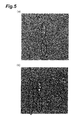
- Fig. 5 is a set of pictures illustrating integrated circuit operation images as a comparative example and an example.
- laser light having a center wavelength of 1300 nm, a wavelength width of 1 nm or less, and an output of 109 mW was emitted, so as to acquire an integrated circuit operation image by LVP, and driven parts were surrounded by ellipses ( Fig. 5(a) ).
- light having a center wavelength of 1310 nm, a wavelength width of 55 nm, and an output of 14 mW was emitted, so as to acquire an integrated circuit operation image by LVP, and driven parts (active parts) were surrounded by ellipses ( Fig. 5(b) ).
- the same integrated circuit was used as the device under test.
- the irradiation with the laser light having the center wavelength of 1300 nm, wavelength width of 1 nm or less, and output of 109 mW when compared with the irradiation with the laser light having the center wavelength of 1300 nm, wavelength width of 1 nm or less, and output of 109 mW, the irradiation with the light having the center wavelength of 1310 nm, wavelength width of 55 nm, and output of 14 mW lowered the noise generated under the influence of the back-reflected light, so that the driven parts were seen even in regions where no driven parts were found when irradiated with the laser light.
- the present invention is not limited thereto.
- the polarizer 6 it is not necessary for the polarizer 6 to be arranged between the SLD 4 and the polarization beam splitter 7.
- a light absorber 16 such as a black member which absorbs these components may be arranged on a side of the polarization beam splitter 7 opposite from the photosensor 12.
- the light generation unit 3 may have a white light source 17 in place of the SLD 4.
- a wavelength-selective filter 18 for adjusting the wavelength width of the light L may be arranged on the optical path of the light L emitted from the white light source 17.
- the control unit 14 functions, together with the wavelength-selective filter 18, as the wavelength width adjustment unit for adjusting the wavelength width of the light L irradiating the integrated circuit 20.
- the control unit 14 regulates the wavelength band of the light L to pass therethrough from the white light source 17, so as to adjust the wavelength width of the light L irradiating the integrated circuit 20. This can also appropriately adjust the wavelength width of the light L irradiating the integrated circuit 20.
- wavelength-selective filters e.g., any of bandpass filters, long-pass filters, and short-pass filters or their combinations
- the present invention can improve the accuracy of inspecting the integrated circuit.
- 1...apparatus for inspecting an integrated circuit 3...light generation unit; 4... superluminescent diode; 5...voltage application unit (wavelength width adjustment unit); 8...scan optical system (irradiation position adjustment unit); 12...photosensor (light detection unit); 14...control unit (wavelength width adjustment unit); 17...white light source; 18...wavelength-selective filter (wavelength width adjustment unit); 20... integrated circuit; 21... silicon substrate (semiconductor substrate); 22...circuit portion; L...light
Landscapes
- General Physics & Mathematics (AREA)
- Physics & Mathematics (AREA)
- Immunology (AREA)
- Pathology (AREA)
- Analytical Chemistry (AREA)
- Biochemistry (AREA)
- General Health & Medical Sciences (AREA)
- Life Sciences & Earth Sciences (AREA)
- Health & Medical Sciences (AREA)
- Chemical & Material Sciences (AREA)
- Engineering & Computer Science (AREA)
- Computer Hardware Design (AREA)
- Microelectronics & Electronic Packaging (AREA)
- General Engineering & Computer Science (AREA)
- Tests Of Electronic Circuits (AREA)
- Testing Or Measuring Of Semiconductors Or The Like (AREA)
Abstract
Description
- The present invention relates to an apparatus for inspecting an integrated circuit.
- As a technique concerning an apparatus for inspecting an integrated circuit,
Patent Literature 1 discloses a technique for irradiating an active region of a transistor formed in the integrated circuit with laser light and detecting the laser light modulated and reflected by the active region of the transistor, thereby analyzing a failure of the transistor. According toPatent Literature 1, the modulation of laser light depends on the transistor's response to a voltage applied to it, so that whether the transistor has a fault or not can be investigated by analyzing the amplitude, intensity, polarization rotation, or phase of the modulated laser light. - [Patent Literature 1]
U.S. Patent Application Publication No. 2010/0039131 - Since the technique disclosed in
Patent Literature 1 irradiates the active region of the transistor with the laser light through the rear face of a semiconductor substrate, however, the laser light reflected by the rear face of the semiconductor substrate may interfere with the laser light modulated and reflected by the active region of the transistor. That is, interference information of the laser light reflected by the rear face may be superposed on signal information of the modulated laser light, so as to lower the S/N ratio. In addition, optical distances vary depending on expansions of the semiconductor substrate and changes in its refractive index caused by temperature variations, whereby the interference information is very hard to stabilize. - It is therefore an object of the present invention to provide an apparatus for inspecting an integrated circuit, which can improve the accuracy of inspecting the integrated circuit.
- The apparatus for inspecting an integrated circuit in accordance with one aspect of the present invention is an apparatus for inspecting an integrated circuit having a semiconductor substrate and a circuit portion formed on a front face side of the semiconductor substrate, the apparatus comprising a light generation unit for generating light for irradiating the integrated circuit, a wavelength width adjustment unit for adjusting a wavelength width of the light for irradiating the integrated circuit, an irradiation position adjustment unit for adjusting an irradiation position of the light for irradiating the integrated circuit, and a light detection unit for detecting light from the integrated circuit when the light from the light generation unit irradiates the circuit portion through a rear face of the semiconductor substrate.
- In this apparatus, the wavelength width of the light irradiating the integrated circuit is adjusted by the wavelength width adjustment unit. This can increase the wavelength width (i.e., decrease the coherence length) according to the distance between the circuit portion and the rear face of the semiconductor substrate, for example, so as to inhibit the light reflected by the rear face of the semiconductor substrate (hereinafter referred to as "back-reflected light") from interfering with light from the circuit portion and its vicinity. That is, interference information of the back-reflected light can be restrained from being superposed on signal information of light from the circuit portion and its vicinity and thus lowering the S/N ratio. Hence, this apparatus can improve the accuracy of inspecting the integrated circuit.
- In the apparatus of the present invention, the light detection unit may detect an intensity of interfering light as the light from the integrated circuit. Since the back-reflected light is inhibited from interfering with the light from the circuit portion and its vicinity as mentioned above, the intensity of the interfering light detected by the light detection unit is mainly attributable to the light from the circuit portion and its vicinity. Therefore, the state of the circuit portion can be analyzed accurately according to the intensity of interfering light detected by the light detection unit.
- In the apparatus of the present invention, the light generation unit may have a superluminescent diode, while the wavelength width adjustment unit may adjust the wavelength width by regulating a voltage applied to the superluminescent diode. Alternatively, the light generation unit may have a white light source, while the wavelength width adjustment unit may adjust the wavelength width by regulating a wavelength band of light to be transmitted therethrough in light from the white light source. These structures can appropriately adjust the wavelength width of the light irradiating the integrated circuit. Light with high luminance can be obtained in particular when the light generation unit has a superluminescent diode.
- In the apparatus of the present invention, the irradiation position adjustment unit may adjust the irradiation position such that the light from the light generation unit irradiates the circuit portion through a depletion layer formed in the semiconductor substrate. In a MOS-type transistor unit, for example, this structure can irradiate the drain with light through the depletion layer, so as to detect the intensity of interfering light caused by light reflected by an interface of the drain on the depletion layer side (formed by a difference in material), light reflected by an interface of the depletion layer on the side opposite from the drain (formed by a difference in carrier density), and the like and thus can analyze the state of the circuit portion accurately.
- In the apparatus of the present invention, the wavelength width adjustment unit may adjust the wavelength width according to a center wavelength of the light irradiating the integrated circuit, a refractive index of the semiconductor substrate, a thickness of the semiconductor substrate, and a depth of the depletion layer. When irradiating the circuit portion with light through the depletion layer, this structure can appropriately adjust the wavelength width of the light irradiating the integrated circuit in order to inhibit the back-reflected light from interfering with the light from the circuit portion and its vicinity and mainly detect the light from the circuit portion and its vicinity.
- The present invention can improve the accuracy of inspecting the integrated circuit.
-
- [
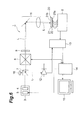
Fig. 1 ] is a structural diagram of the apparatus for inspecting an integrated circuit in accordance with an embodiment of the present invention; - [
Fig. 2 ] is a structural diagram of a part of an integrated circuit which is a device under test by the apparatus ofFig. 1 ; - [
Fig. 3 ] is an explanatory view of making an integrated circuit operation image by using the apparatus ofFig. 1 ; - [
Fig. 4 ] is an explanatory view of making an integrated circuit operation image by using the apparatus ofFig. 1 ; - [
Fig. 5 ] is a set of pictures illustrating integrated circuit operation images as a comparative example and an example; - [
Fig. 6 ] is a structural diagram of the apparatus for inspecting an integrated circuit in accordance with another embodiment of the present invention; and - [
Fig. 7 ] is a structural diagram of the apparatus for inspecting an integrated circuit in accordance with still another embodiment of the present invention. - In the following, preferred embodiments of the present invention will be explained in detail with reference to the drawings. In the drawings, the same or equivalent parts will be referred to with the same signs while omitting their overlapping descriptions.
- As illustrated in
Fig. 1 , anapparatus 1 for inspecting an integrated circuit is an apparatus for inspecting an integratedcircuit 20, which is a device under test (DUT), so as to specify a location where an abnormality occurs, and so forth. Theintegrated circuit 20, an example of which is a C-MOS-IC, for example, having a silicon substrate (semiconductor substrate) 21 and acircuit portion 22 formed on afront face 21a side of thesilicon substrate 21. A test signal (e.g., a pulse signal in a rectangular wave form) is fed into the integratedcircuit 20, so as to drive the latter at the time of inspection. - The
apparatus 1 is equipped with alight generation unit 3 for generating light L for irradiating the integratedcircuit 20. Thelight generation unit 3 has a superluminescent diode (hereinafter referred to as "SLD") 4 and avoltage application unit 5 for applying a voltage to theSLD 4. The light L emitted from theSLD 4 when the voltage is applied thereto by thevoltage application unit 5 is collimated into parallel light by a lens system and then exits from thelight generation unit 3. - The light L exiting from the
light generation unit 3 is converted by apolarizer 6 into linearly polarized light having a predetermined polarization direction. The light L transmitted through thepolarizer 6 passes through apolarization beam splitter 7 and a scan optical system (irradiation position adjustment unit) 8 in sequence and then is converted by a quarter-wave plate 9 into circularly polarized light. The light L transmitted through the quarter-wave plate 9 forms an image at a predetermined position of the integratedcircuit 20 through an image-formingoptical system 11 including a mirror, a lens, and the like. At this time, the light L irradiates thecircuit portion 22 through therear face 21b of thesilicon substrate 21. The scanoptical system 8 two-dimensionally scans theintegrated circuit 20 with the light L. That is, the scanoptical system 8 adjusts the irradiation position of the light L irradiating theintegrated circuit 20. - The light L reflected by the
integrated circuit 20 passes through the image-formingoptical system 11, so as to be converted by the quarter-wave plate 9 into linearly polarized light. The light L transmitted through the quarter-wave plate 9 passes through the scanoptical system 8 but has a polarization direction perpendicular to the above-mentioned predetermined polarization direction, so as to be reflected by thepolarization beam splitter 7, thereby being detected by a photosensor (light detection unit) 12. That is, when the light L from thelight generation unit 3 irradiates thecircuit portion 22 through therear face 21b of thesilicon substrate 21, thephotosensor 12 detects the light L from theintegrated circuit 20. Here, thephotosensor 12 detects the intensity of interfering light as the light L from theintegrated circuit 20. - An electric signal issued from the
photosensor 12 in response to an input of the optical signal is amplified and then fed into a lock-inamplifier 13. According to the test signal fed from thetester 2 to theintegrated circuit 20, the lock-inamplifier 13 extracts a signal corresponding to a specific period from the optical signal. Thus extracted signal is fed into acontrol unit 14 which controls individual parts of theapparatus 1 such as the scanoptical system 8. Thecontrol unit 14 turns the input signal into an image in association with the position at which the integratedcircuit 20 is irradiated with the light L. Thus produced integrated circuit operation image is shown on adisplay 15. A spectrum analyzer may be used in place of the lock-inamplifier 13. - The
control unit 14 functions not only as an analysis unit, but also, together with thevoltage application unit 5, as a wavelength width adjustment unit for adjusting the wavelength width of the light L irradiating theintegrated circuit 20. That is, by controlling thevoltage application unit 5 so as to regulate the voltage applied to theSLD 4, thecontrol unit 14 adjusts the wavelength width of the light L irradiating theintegrated circuit 20. TheSLD 4 has such a characteristic as to emit the light L with narrower wavelength width as the voltage applied by thevoltage application unit 5 is higher. - The wavelength width of the light L adjusted by the
control unit 14 will now be explained with reference toFig. 2. Fig. 2 is a structural diagram of a MOS-type transistor unit which is a part of theintegrated circuit 20. The position at which the integratedcircuit 20 is irradiated with the light L is adjusted by the scanoptical system 8 such that the circuit portion 22 (drain here) is irradiated with the light L through a depletion layer formed in thesilicon substrate 21. - First, the
coherence length 1 of light L is represented by the following expression:
- The intensity modulation of a signal effective in making the above-mentioned integrated circuit operation image is about several tens of ppm. That is, for reducing the noise relative to the signal so as to secure a sufficient S/N ratio, it is necessary for the
coherence length 1 to be sufficiently small as compared with the optical path length difference between the component of light L reflected by the surface to be observed (i.e., the surface of thecircuit portion 22 and its vicinity) and the component of light L reflected by the other surface (i.e., therear face 21b of the silicon substrate 21). The intensity I of interfering light is represented by the following expression:
where x is the distance from a position where the intensity I is maximized. - When |x| > 1, assuming that the maximum value of intensity I is 1, the intensity I is approximately within the range of

and, on average,
- For improving the S/N ratio, it is necessary for the intensity I of interfering light between the component of light L reflected by the surface to be observed and the component of light L reflected by the other surface to be as low as possible. In order for the intensity I to be 0.001, for example, the distance x may be about 14. For suppressing the interference with the component of light L reflected by the
rear face 21b of thesilicon substrate 21, it is necessary for the optical path length by which the light L travels back and forth through thesilicon substrate 21 to exceed thecoherence length 1. - That is, letting T be the thickness of the
silicon substrate 21, and n be the refractive index of thesilicon substrate 21 with respect to the light L, it is necessary to satisfy

- The refractive index n of the
silicon substrate 21 is about 3.5. The center wavelength (observation wavelength) of the light L is preferably as short as possible without being absorbed by thesilicon substrate 21 and thus is typically 1.3 µm. In this case, the wavelength width d of the light L is represented by
When the thickness T of thesilicon substrate 21 is 100 µm, it is necessary for the wavelength width d of the light L to exceed 33.8 nm. - Thus making the light L have the broader wavelength width d and
shorter coherence length 1 can inhibit the back-reflected light (the component of light L reflected by therear face 21b of the silicon substrate 21) from interfering with the component of light L reflected by the surface of thecircuit portion 22 and its vicinity. - On the other hand, the modulation of the reflected light of the light L is based on the change in reflectance on the surface of the
circuit portion 22 and its vicinity, and this change is caused by the movement of the reflecting surface due to the expansion/shrinkage of the depletion layer near thecircuit portion 22 and the light absorption by its inner carriers. That is, for preventing the change in reflectance from decreasing, acoherence length 1 which corresponds to 2 times the depth of the depletion layer (the distance between the interface of the drain on the depletion layer side and the interface of the depletion layer on the side opposite from the drain) multiplied by the refractive index n is necessary. This distance is in proportion to the square root of the voltage between regions in contact with each other and in reverse proportion to the carrier density. Letting t be the depth of the depletion layer accompanying a diffusion layer, the following expression holds:
- Letting the refractive index n of the
silicon substrate 21 be 3.5, and the center wavelength of the light L be 1.3 µm as mentioned above, approximately
- Hence, an appropriate wavelength width d of the light L is represented by

- When observing also the voltage of a deep diffusion layer (well structure) or the like, assuming that the depth t of the depletion layer and the thickness T of the
silicon substrate 21 are 1 µm and 100 µm, respectively, the appropriate wavelength width d of the light L is represented by
- As in the foregoing, the
control unit 14 determines the value of wavelength width d of the light L according to the center wavelength λ of the light L irradiating theintegrated circuit 20, the refractive index n of thesilicon substrate 21, the thickness T of thesilicon substrate 21, and the depth t of the depletion layer. Thecontrol unit 14 controls thevoltage application unit 5, so as to regulate the voltage applied to theSLD 4, thereby adjusting the wavelength width d of the light L such that it attains the determined value. - The making of the above-mentioned integrated circuit operation image will now be explained. Here, the making of the integrated circuit operation image is based on the LVI (Laser Voltage Imaging) method (see, for example, Patent Literature 1).
- First, the
tester 2 feeds the test signal to theintegrated circuit 20, so as to drive the latter. In this state, as illustrated inFig. 3 , the position where theintegrated circuit 20 is irradiated with the light L is placed at a position P1 by the scanoptical system 8, and the intensity of interfering light is detected by thephotosensor 12. Then, the lock-inamplifier 13 analyzes the intensity signal of the interfering light in synchronization with the test signal, so as to detect the intensity I1 of the interfering light at a specific frequency f0. - Subsequently, as illustrated in
Fig. 4 , the position where theintegrated circuit 20 is irradiated with the light L is placed at a position P2 by the scanoptical system 8, and the intensity of interfering light is detected by thephotosensor 12. Then, the lock-inamplifier 13 analyzes the intensity signal of the interfering light in synchronization with the test signal, so as to detect the intensity I2 of the interfering light at the specific frequency f0. - Thus, the
integrated circuit 20 is two-dimensionally scanned with the irradiation position of the light L, so as to detect the intensity I2 at the specific frequency f0 in the entireintegrated circuit 20. Then, thecontrol unit 14 associates the intensity of interfering light with the irradiation position of the light L, so that an interfering light intensity image at the specific frequency f0 is made as an integrated circuit operation image, which is shown on thedisplay 15. - Whether the
integrated circuit 20 is driven or not alters the range where carriers exist in thecircuit portion 22, thereby modifying the depth of the depletion layer, its light absorptance, and the like. This changes the optical path length of the light L reflected by the interface of the depletion layer on the side opposite from the drain. Therefore, a change in intensity (intensity modulation) of the light L exists between the cases where theintegrated circuit 20 is driven and not, whereas the intensity of the light L reflected by the interface does not change at a location where an abnormality occurs. Hence, detecting the intensity of the interfering light can specify the location where the abnormality occurs in theintegrated circuit 20. The irradiation position of the light L may be placed at a specific location in theintegrated circuit 20, so as to detect the intensity of the interfering light at this location, thereby inspecting the location. - In the
apparatus 1, as explained in the foregoing, the wavelength width of the light L irradiating theintegrated circuit 20 is adjusted by thecontrol unit 14 andvoltage application unit 5. This can increase the wavelength width (i.e., decrease the coherence length) according to the distance between thecircuit portion 22 and therear face 21 b of thesilicon substrate 21, so as to inhibit the back-reflected light from interfering with the light L from thecircuit portion 22 and its vicinity. That is, interference information of the back-reflected light can be restrained from being superposed on signal information of the light L from thecircuit portion 22 and its vicinity and thus lowering the S/N ratio. Hence, theapparatus 1 can improve the accuracy of inspecting theintegrated circuit 20. - The
light generation unit 3 has theSLD 4, while thecontrol unit 14 controls thevoltage application unit 5, so as to regulate the voltage applied to theSLD 4, thereby adjusting the wavelength width of the light L irradiating theintegrated circuit 20. This can appropriately adjust the wavelength width of the light L irradiating theintegrated circuit 20. Using theSLD 4 can yield the light L with high luminance in particular. - A wavelength-selective filter for adjusting the wavelength width of the light L may be arranged on an optical path of the light L emitted from the
SLD 4. In this case, thecontrol unit 14 functions, together with the wavelength-selective filter, as the wavelength width adjustment unit for adjusting the wavelength width of the light L irradiating theintegrated circuit 20. That is, by switching among several kinds of wavelength-selective filters (e.g., any of bandpass filters, long-pass filters, and short-pass filters or their combinations), for example, thecontrol unit 14 regulates the wavelength band of the light L to pass therethrough from theSLD 4, so as to adjust the wavelength width of the light L irradiating theintegrated circuit 20. This can also appropriately adjust the wavelength width of the light L irradiating theintegrated circuit 20. - Here, the
control unit 14 determines the value of wavelength width of the light L irradiating theintegrated circuit 20 according to the center wavelength of the light L, the refractive index of thesilicon substrate 21, the thickness of thesilicon substrate 21, and the depth of the depletion layer. This can appropriately adjust the wavelength width of the light L irradiating theintegrated circuit 20 in order to inhibit the back-reflected light from interfering with the light L from thecircuit portion 22 and its vicinity and mainly detect the light L from thecircuit portion 22 and its vicinity. - The scan
optical system 8 adjusts the irradiation position of the light L such that the light L from thelight generation unit 3 irradiates thecircuit portion 22 through the depletion layer formed in thesilicon substrate 21. In a MOS-type transistor unit, for example, this structure can irradiate the drain with the light L through the depletion layer, so as to detect the intensity of interfering light caused by light reflected by an interface of the drain on the depletion layer side (formed by a difference in material), light reflected by an interface of the depletion layer on the side opposite from the drain (formed by a difference in carrier density), and the like and thus can analyze the state of thecircuit portion 22 accurately. The width of a channel region between the source and drain has recently been becoming narrower than the wavelength of the light L as theintegrated circuit 20 has been made finer, so that the light L is harder to be incident on this region, whereby the above-mentioned structure can be very effective. Thecircuit portion 22 may also be irradiated with the light L from thelight generation unit 3 through a depletion layer directly under the channel region. -
Fig. 5 is a set of pictures illustrating integrated circuit operation images as a comparative example and an example. As the comparative example, laser light having a center wavelength of 1300 nm, a wavelength width of 1 nm or less, and an output of 109 mW was emitted, so as to acquire an integrated circuit operation image by LVP, and driven parts were surrounded by ellipses (Fig. 5(a) ). As the example, on the other hand, light having a center wavelength of 1310 nm, a wavelength width of 55 nm, and an output of 14 mW was emitted, so as to acquire an integrated circuit operation image by LVP, and driven parts (active parts) were surrounded by ellipses (Fig. 5(b) ). The same integrated circuit was used as the device under test. As a result, when compared with the irradiation with the laser light having the center wavelength of 1300 nm, wavelength width of 1 nm or less, and output of 109 mW, the irradiation with the light having the center wavelength of 1310 nm, wavelength width of 55 nm, and output of 14 mW lowered the noise generated under the influence of the back-reflected light, so that the driven parts were seen even in regions where no driven parts were found when irradiated with the laser light. - Though an embodiment of the present invention has been explained in the foregoing, the present invention is not limited thereto. For example, as illustrated in
Fig. 6 , it is not necessary for thepolarizer 6 to be arranged between theSLD 4 and thepolarization beam splitter 7. In this case, for preventing nonlinearly polarized components in the light L emitted from theSLD 4 from being directed to the photosensor 12 as scattered light, alight absorber 16 such as a black member which absorbs these components may be arranged on a side of thepolarization beam splitter 7 opposite from thephotosensor 12. - As illustrated in
Fig. 7 , thelight generation unit 3 may have awhite light source 17 in place of theSLD 4. In this case, a wavelength-selective filter 18 for adjusting the wavelength width of the light L may be arranged on the optical path of the light L emitted from thewhite light source 17. Here, thecontrol unit 14 functions, together with the wavelength-selective filter 18, as the wavelength width adjustment unit for adjusting the wavelength width of the light L irradiating theintegrated circuit 20. That is, by switching among several kinds of wavelength-selective filters (e.g., any of bandpass filters, long-pass filters, and short-pass filters or their combinations), for example, thecontrol unit 14 regulates the wavelength band of the light L to pass therethrough from thewhite light source 17, so as to adjust the wavelength width of the light L irradiating theintegrated circuit 20. This can also appropriately adjust the wavelength width of the light L irradiating theintegrated circuit 20. - The present invention can improve the accuracy of inspecting the integrated circuit.
- 1...apparatus for inspecting an integrated circuit; 3...light generation unit; 4... superluminescent diode; 5...voltage application unit (wavelength width adjustment unit); 8...scan optical system (irradiation position adjustment unit); 12...photosensor (light detection unit); 14...control unit (wavelength width adjustment unit); 17...white light source; 18...wavelength-selective filter (wavelength width adjustment unit); 20... integrated circuit; 21... silicon substrate (semiconductor substrate); 22...circuit portion; L...light
Claims (6)
- An apparatus for inspecting an integrated circuit having a semiconductor substrate and a circuit portion formed on a front face side of the semiconductor substrate, the apparatus comprising:a light generation unit for generating light for irradiating the integrated circuit;a wavelength width adjustment unit for adjusting a wavelength width of the light for irradiating the integrated circuit;an irradiation position adjustment unit for adjusting an irradiation position of the light for irradiating the integrated circuit; anda light detection unit for detecting light from the integrated circuit when the light from the light generation unit irradiates the circuit portion through a rear face of the semiconductor substrate.
- The apparatus according to claim 1, wherein the light detection unit detects an intensity of interfering light as the light from the integrated circuit.
- The apparatus according to claim 1 or 2, wherein the light generation unit has a superluminescent diode; and
wherein the wavelength width adjustment unit adjusts the wavelength width by regulating a voltage applied to the superluminescent diode. - The apparatus according to claim 1 or 2, wherein the light generation unit has a white light source; and
wherein the wavelength width adjustment unit adjusts the wavelength width by regulating a wavelength band of light to be transmitted therethrough in light from the white light source. - The apparatus according to any one of claims 1 to 4, wherein the irradiation position adjustment unit adjusts the irradiation position such that the light from the light generation unit irradiates the circuit portion through a depletion layer formed in the semiconductor substrate.
- The apparatus according to claim 5, wherein the wavelength width adjustment unit adjusts the wavelength width according to a center wavelength of the light irradiating the integrated circuit, a refractive index of the semiconductor substrate, a thickness of the semiconductor substrate, and a depth of the depletion layer.
Applications Claiming Priority (2)
| Application Number | Priority Date | Filing Date | Title |
|---|---|---|---|
| JP2011121893A JP5894745B2 (en) | 2011-05-31 | 2011-05-31 | Integrated circuit inspection equipment |
| PCT/JP2012/063521 WO2012165344A1 (en) | 2011-05-31 | 2012-05-25 | Integrated circuit inspection device |
Publications (3)
| Publication Number | Publication Date |
|---|---|
| EP2717305A1 true EP2717305A1 (en) | 2014-04-09 |
| EP2717305A4 EP2717305A4 (en) | 2015-03-11 |
| EP2717305B1 EP2717305B1 (en) | 2020-03-18 |
Family
ID=47259200
Family Applications (1)
| Application Number | Title | Priority Date | Filing Date |
|---|---|---|---|
| EP12793492.5A Active EP2717305B1 (en) | 2011-05-31 | 2012-05-25 | Method of integrated circuit inspection |
Country Status (7)
| Country | Link |
|---|---|
| US (2) | US9099350B2 (en) |
| EP (1) | EP2717305B1 (en) |
| JP (1) | JP5894745B2 (en) |
| KR (1) | KR101951969B1 (en) |
| CN (2) | CN106198566B (en) |
| TW (1) | TWI557415B (en) |
| WO (1) | WO2012165344A1 (en) |
Families Citing this family (17)
| Publication number | Priority date | Publication date | Assignee | Title |
|---|---|---|---|---|
| JP5894745B2 (en) | 2011-05-31 | 2016-03-30 | 浜松ホトニクス株式会社 | Integrated circuit inspection equipment |
| WO2014119676A1 (en) | 2013-02-01 | 2014-08-07 | 浜松ホトニクス株式会社 | Semiconductor device inspection device and semiconductor device inspection method |
| US10191111B2 (en) * | 2013-03-24 | 2019-01-29 | Dcg Systems, Inc. | Synchronized pulsed LADA for the simultaneous acquisition of timing diagrams and laser-induced upsets |
| JP6283501B2 (en) | 2013-11-12 | 2018-02-21 | 浜松ホトニクス株式会社 | Frequency analysis apparatus and frequency analysis method |
| JP6283507B2 (en) | 2013-11-29 | 2018-02-21 | 浜松ホトニクス株式会社 | Semiconductor device measuring apparatus and semiconductor device measuring method |
| TWI619954B (en) * | 2014-10-16 | 2018-04-01 | Dcg系統公司 | Systems and method for laser voltage imaging |
| CN107615603B (en) * | 2015-05-29 | 2024-06-04 | 浜松光子学株式会社 | Light source device and inspection device |
| JP2016223899A (en) * | 2015-05-29 | 2016-12-28 | 浜松ホトニクス株式会社 | Light source device and inspection device |
| CN108701623B (en) * | 2015-11-05 | 2022-10-04 | 米朋克斯株式会社 | Substrate evaluation method |
| KR102255480B1 (en) * | 2015-11-06 | 2021-05-24 | 에프이아이 컴파니 | Waveform Mapping and Gated Laser Voltage Imaging |
| JP6194380B2 (en) * | 2016-02-29 | 2017-09-06 | 浜松ホトニクス株式会社 | Integrated circuit inspection equipment |
| US10132861B2 (en) * | 2016-09-16 | 2018-11-20 | Qualcomm Incorporated | Visible laser circuit fault isolation |
| DE102018108283A1 (en) * | 2018-04-09 | 2019-10-10 | Carl Zeiss Smt Gmbh | Electro-optical circuit board for contacting photonic integrated circuits |
| JP7158224B2 (en) * | 2018-09-26 | 2022-10-21 | 浜松ホトニクス株式会社 | Semiconductor device inspection method and semiconductor device inspection apparatus |
| JP7398449B2 (en) * | 2019-05-31 | 2023-12-14 | 浜松ホトニクス株式会社 | Semiconductor device testing method and semiconductor device testing equipment |
| US12599020B2 (en) | 2021-06-01 | 2026-04-07 | Kulicke And Soffa Industries, Inc. | Electronic component bonding machines, and methods of measuring a distance on such machines |
| TWI831087B (en) * | 2021-11-25 | 2024-02-01 | 一品光學工業股份有限公司 | Optical sensing device |
Family Cites Families (28)
| Publication number | Priority date | Publication date | Assignee | Title |
|---|---|---|---|---|
| US4856014A (en) * | 1986-12-31 | 1989-08-08 | Trw Inc. | Angled stripe superluminescent diode |
| US5126660A (en) | 1991-01-02 | 1992-06-30 | At&T Bell Laboratories | Optical probing method and apparatus |
| JPH06102295A (en) | 1992-07-28 | 1994-04-15 | Hewlett Packard Co <Hp> | Non-contact type probe and non-contact voltage measuring device |
| US6376329B1 (en) * | 1997-08-04 | 2002-04-23 | Nikon Corporation | Semiconductor wafer alignment using backside illumination |
| US5956142A (en) * | 1997-09-25 | 1999-09-21 | Siemens Aktiengesellschaft | Method of end point detection using a sinusoidal interference signal for a wet etch process |
| US6184542B1 (en) * | 1998-06-16 | 2001-02-06 | Princeton Lightwave | Superluminescent diode and optical amplifier with extended bandwidth |
| US6633376B1 (en) * | 1998-08-10 | 2003-10-14 | Mitsubishi Denki Kabushiki Kaisha | Apparatus for inspecting a printed circuit board |
| JP3610837B2 (en) * | 1998-09-18 | 2005-01-19 | 株式会社日立製作所 | Sample surface observation method and apparatus, defect inspection method and apparatus |
| US6690469B1 (en) * | 1998-09-18 | 2004-02-10 | Hitachi, Ltd. | Method and apparatus for observing and inspecting defects |
| GB0206342D0 (en) * | 2002-03-18 | 2002-05-01 | Murgitroyd & Company | An improved process control method and apparatus |
| US7420675B2 (en) * | 2003-06-25 | 2008-09-02 | The University Of Akron | Multi-wavelength imaging system |
| JP2005077964A (en) * | 2003-09-03 | 2005-03-24 | Fujitsu Ltd | Spectroscope apparatus |
| GB0415766D0 (en) * | 2004-07-14 | 2004-08-18 | Taylor Hobson Ltd | Apparatus for and a method of determining a characteristic of a layer or layers |
| US7924892B2 (en) * | 2004-08-25 | 2011-04-12 | Kla-Tencor Technologies Corporation | Fiber amplifier based light source for semiconductor inspection |
| US7884024B2 (en) * | 2005-02-24 | 2011-02-08 | Dcg Systems, Inc. | Apparatus and method for optical interference fringe based integrated circuit processing |
| TW200717678A (en) * | 2005-05-05 | 2007-05-01 | Koninkl Philips Electronics Nv | Method for analyzing an integrated circuit, apparatus and integrated circuit |
| US7659981B2 (en) * | 2005-08-26 | 2010-02-09 | Dcg Systems, Inc. | Apparatus and method for probing integrated circuits using polarization difference probing |
| US7450245B2 (en) | 2005-06-29 | 2008-11-11 | Dcg Systems, Inc. | Method and apparatus for measuring high-bandwidth electrical signals using modulation in an optical probing system |
| US7616312B2 (en) | 2005-06-29 | 2009-11-10 | Dcg Systems, Inc. | Apparatus and method for probing integrated circuits using laser illumination |
| US7733100B2 (en) * | 2005-08-26 | 2010-06-08 | Dcg Systems, Inc. | System and method for modulation mapping |
| US7659973B2 (en) * | 2006-05-26 | 2010-02-09 | Applied Materials Southeast Asia, Pte Ltd. | Wafer inspection using short-pulsed continuous broadband illumination |
| JP5396004B2 (en) * | 2007-01-31 | 2014-01-22 | オリンパス株式会社 | Fluorescence observation apparatus and method of operating fluorescence observation apparatus |
| US7570366B2 (en) * | 2007-02-21 | 2009-08-04 | Corning Incorporated | Apparatus for measuring defects in a glass sheet |
| KR100884353B1 (en) * | 2007-09-18 | 2009-02-18 | 한국전자통신연구원 | High Brightness Diode and Method of Manufacturing the Same |
| US8045251B2 (en) * | 2007-12-06 | 2011-10-25 | The Boeing Company | Coherence length controller |
| TWI358538B (en) * | 2008-02-22 | 2012-02-21 | Ind Tech Res Inst | Apparatus for measuring defects in semiconductor w |
| US8248617B2 (en) * | 2008-04-22 | 2012-08-21 | Zygo Corporation | Interferometer for overlay measurements |
| JP5894745B2 (en) | 2011-05-31 | 2016-03-30 | 浜松ホトニクス株式会社 | Integrated circuit inspection equipment |
-
2011
- 2011-05-31 JP JP2011121893A patent/JP5894745B2/en active Active
-
2012
- 2012-05-25 WO PCT/JP2012/063521 patent/WO2012165344A1/en not_active Ceased
- 2012-05-25 KR KR1020137030653A patent/KR101951969B1/en active Active
- 2012-05-25 EP EP12793492.5A patent/EP2717305B1/en active Active
- 2012-05-25 CN CN201610452908.5A patent/CN106198566B/en active Active
- 2012-05-25 CN CN201280026635.8A patent/CN103563064B/en active Active
- 2012-05-30 TW TW101119392A patent/TWI557415B/en active
- 2012-05-31 US US13/485,016 patent/US9099350B2/en active Active
-
2015
- 2015-06-26 US US14/751,637 patent/US10508996B2/en active Active
Also Published As
| Publication number | Publication date |
|---|---|
| TWI557415B (en) | 2016-11-11 |
| CN103563064A (en) | 2014-02-05 |
| JP5894745B2 (en) | 2016-03-30 |
| CN106198566A (en) | 2016-12-07 |
| CN106198566B (en) | 2020-08-21 |
| JP2012247397A (en) | 2012-12-13 |
| CN103563064B (en) | 2016-08-17 |
| EP2717305A4 (en) | 2015-03-11 |
| TW201303332A (en) | 2013-01-16 |
| EP2717305B1 (en) | 2020-03-18 |
| US20120307249A1 (en) | 2012-12-06 |
| US20150293036A1 (en) | 2015-10-15 |
| KR101951969B1 (en) | 2019-02-25 |
| KR20140033368A (en) | 2014-03-18 |
| WO2012165344A1 (en) | 2012-12-06 |
| US10508996B2 (en) | 2019-12-17 |
| US9099350B2 (en) | 2015-08-04 |
Similar Documents
| Publication | Publication Date | Title |
|---|---|---|
| EP2717305A1 (en) | Integrated circuit inspection device | |
| US6483594B2 (en) | Apparatus and method for determining the active dopant profile in a semiconductor wafer | |
| CN107615603B (en) | Light source device and inspection device | |
| JPH05281141A (en) | Method and apparatus for measuring photoluminescence in crystal | |
| CN101551324A (en) | Device and method for measuring characteristics of semiconductor materials based on dual probe beams | |
| KR102530265B1 (en) | Carrier lifetime measurement method and carrier lifetime measurement device | |
| KR20080091085A (en) | Characteristic method by light reflectance of strain and active dopant in semiconductor structure | |
| US7212288B2 (en) | Position modulated optical reflectance measurement system for semiconductor metrology | |
| US20040104352A1 (en) | Modulated reflectance measurement system using UV probe | |
| JPWO2005022180A1 (en) | Method and apparatus for measuring electric field distribution of semiconductor device | |
| WO2003046519A1 (en) | Delay time modulation femtosecond time-resolved scanning probe microscope apparatus | |
| KR20200118791A (en) | Concentration measuring method and concentration measuring device | |
| US20050099623A1 (en) | Optical measuring method for semiconductor multiple layer structures and apparatus therefor | |
| JP6194380B2 (en) | Integrated circuit inspection equipment | |
| US6356381B1 (en) | Multi-wavelength cross-correlator for ultrashort radiation pulses | |
| US7906764B2 (en) | Measuring apparatus using terahertz wave | |
| US20080074668A1 (en) | Modulated optical reflectance measurement system with enhanced sensitivity | |
| US7230245B2 (en) | Field induced THz wave emission microscope | |
| JP2012002793A (en) | Terahertz wave measuring apparatus and terahertz wave measuring method | |
| JP2004125584A (en) | Optical modulation excitation reflection spectrometer |
Legal Events
| Date | Code | Title | Description |
|---|---|---|---|
| PUAI | Public reference made under article 153(3) epc to a published international application that has entered the european phase |
Free format text: ORIGINAL CODE: 0009012 |
|
| 17P | Request for examination filed |
Effective date: 20131126 |
|
| AK | Designated contracting states |
Kind code of ref document: A1 Designated state(s): AL AT BE BG CH CY CZ DE DK EE ES FI FR GB GR HR HU IE IS IT LI LT LU LV MC MK MT NL NO PL PT RO RS SE SI SK SM TR |
|
| RAP1 | Party data changed (applicant data changed or rights of an application transferred) |
Owner name: HAMAMATSU PHOTONICS K.K. |
|
| DAX | Request for extension of the european patent (deleted) | ||
| A4 | Supplementary search report drawn up and despatched |
Effective date: 20150205 |
|
| RIC1 | Information provided on ipc code assigned before grant |
Ipc: H01L 21/66 20060101AFI20150130BHEP Ipc: G01N 21/55 20140101ALI20150130BHEP Ipc: G01N 21/956 20060101ALI20150130BHEP Ipc: G01N 21/88 20060101ALI20150130BHEP |
|
| STAA | Information on the status of an ep patent application or granted ep patent |
Free format text: STATUS: EXAMINATION IS IN PROGRESS |
|
| 17Q | First examination report despatched |
Effective date: 20170406 |
|
| REG | Reference to a national code |
Ref country code: DE Ref legal event code: R079 Ref document number: 602012068595 Country of ref document: DE Free format text: PREVIOUS MAIN CLASS: H01L0021660000 Ipc: G01N0021550000 |
|
| GRAP | Despatch of communication of intention to grant a patent |
Free format text: ORIGINAL CODE: EPIDOSNIGR1 |
|
| STAA | Information on the status of an ep patent application or granted ep patent |
Free format text: STATUS: GRANT OF PATENT IS INTENDED |
|
| RIC1 | Information provided on ipc code assigned before grant |
Ipc: G01N 21/88 20060101ALI20191122BHEP Ipc: G01N 21/55 20140101AFI20191122BHEP Ipc: H01L 21/66 20060101ALI20191122BHEP |
|
| INTG | Intention to grant announced |
Effective date: 20191213 |
|
| GRAS | Grant fee paid |
Free format text: ORIGINAL CODE: EPIDOSNIGR3 |
|
| GRAA | (expected) grant |
Free format text: ORIGINAL CODE: 0009210 |
|
| STAA | Information on the status of an ep patent application or granted ep patent |
Free format text: STATUS: THE PATENT HAS BEEN GRANTED |
|
| AK | Designated contracting states |
Kind code of ref document: B1 Designated state(s): AL AT BE BG CH CY CZ DE DK EE ES FI FR GB GR HR HU IE IS IT LI LT LU LV MC MK MT NL NO PL PT RO RS SE SI SK SM TR |
|
| REG | Reference to a national code |
Ref country code: GB Ref legal event code: FG4D |
|
| REG | Reference to a national code |
Ref country code: DE Ref legal event code: R096 Ref document number: 602012068595 Country of ref document: DE |
|
| REG | Reference to a national code |
Ref country code: AT Ref legal event code: REF Ref document number: 1246477 Country of ref document: AT Kind code of ref document: T Effective date: 20200415 Ref country code: IE Ref legal event code: FG4D |
|
| REG | Reference to a national code |
Ref country code: NL Ref legal event code: FP |
|
| PG25 | Lapsed in a contracting state [announced via postgrant information from national office to epo] |
Ref country code: RS Free format text: LAPSE BECAUSE OF FAILURE TO SUBMIT A TRANSLATION OF THE DESCRIPTION OR TO PAY THE FEE WITHIN THE PRESCRIBED TIME-LIMIT Effective date: 20200318 Ref country code: FI Free format text: LAPSE BECAUSE OF FAILURE TO SUBMIT A TRANSLATION OF THE DESCRIPTION OR TO PAY THE FEE WITHIN THE PRESCRIBED TIME-LIMIT Effective date: 20200318 Ref country code: NO Free format text: LAPSE BECAUSE OF FAILURE TO SUBMIT A TRANSLATION OF THE DESCRIPTION OR TO PAY THE FEE WITHIN THE PRESCRIBED TIME-LIMIT Effective date: 20200618 |
|
| PG25 | Lapsed in a contracting state [announced via postgrant information from national office to epo] |
Ref country code: HR Free format text: LAPSE BECAUSE OF FAILURE TO SUBMIT A TRANSLATION OF THE DESCRIPTION OR TO PAY THE FEE WITHIN THE PRESCRIBED TIME-LIMIT Effective date: 20200318 Ref country code: BG Free format text: LAPSE BECAUSE OF FAILURE TO SUBMIT A TRANSLATION OF THE DESCRIPTION OR TO PAY THE FEE WITHIN THE PRESCRIBED TIME-LIMIT Effective date: 20200618 Ref country code: GR Free format text: LAPSE BECAUSE OF FAILURE TO SUBMIT A TRANSLATION OF THE DESCRIPTION OR TO PAY THE FEE WITHIN THE PRESCRIBED TIME-LIMIT Effective date: 20200619 Ref country code: SE Free format text: LAPSE BECAUSE OF FAILURE TO SUBMIT A TRANSLATION OF THE DESCRIPTION OR TO PAY THE FEE WITHIN THE PRESCRIBED TIME-LIMIT Effective date: 20200318 Ref country code: LV Free format text: LAPSE BECAUSE OF FAILURE TO SUBMIT A TRANSLATION OF THE DESCRIPTION OR TO PAY THE FEE WITHIN THE PRESCRIBED TIME-LIMIT Effective date: 20200318 |
|
| REG | Reference to a national code |
Ref country code: LT Ref legal event code: MG4D |
|
| PG25 | Lapsed in a contracting state [announced via postgrant information from national office to epo] |
Ref country code: IS Free format text: LAPSE BECAUSE OF FAILURE TO SUBMIT A TRANSLATION OF THE DESCRIPTION OR TO PAY THE FEE WITHIN THE PRESCRIBED TIME-LIMIT Effective date: 20200718 Ref country code: SK Free format text: LAPSE BECAUSE OF FAILURE TO SUBMIT A TRANSLATION OF THE DESCRIPTION OR TO PAY THE FEE WITHIN THE PRESCRIBED TIME-LIMIT Effective date: 20200318 Ref country code: RO Free format text: LAPSE BECAUSE OF FAILURE TO SUBMIT A TRANSLATION OF THE DESCRIPTION OR TO PAY THE FEE WITHIN THE PRESCRIBED TIME-LIMIT Effective date: 20200318 Ref country code: CZ Free format text: LAPSE BECAUSE OF FAILURE TO SUBMIT A TRANSLATION OF THE DESCRIPTION OR TO PAY THE FEE WITHIN THE PRESCRIBED TIME-LIMIT Effective date: 20200318 Ref country code: EE Free format text: LAPSE BECAUSE OF FAILURE TO SUBMIT A TRANSLATION OF THE DESCRIPTION OR TO PAY THE FEE WITHIN THE PRESCRIBED TIME-LIMIT Effective date: 20200318 Ref country code: SM Free format text: LAPSE BECAUSE OF FAILURE TO SUBMIT A TRANSLATION OF THE DESCRIPTION OR TO PAY THE FEE WITHIN THE PRESCRIBED TIME-LIMIT Effective date: 20200318 Ref country code: PT Free format text: LAPSE BECAUSE OF FAILURE TO SUBMIT A TRANSLATION OF THE DESCRIPTION OR TO PAY THE FEE WITHIN THE PRESCRIBED TIME-LIMIT Effective date: 20200812 Ref country code: LT Free format text: LAPSE BECAUSE OF FAILURE TO SUBMIT A TRANSLATION OF THE DESCRIPTION OR TO PAY THE FEE WITHIN THE PRESCRIBED TIME-LIMIT Effective date: 20200318 |
|
| REG | Reference to a national code |
Ref country code: AT Ref legal event code: MK05 Ref document number: 1246477 Country of ref document: AT Kind code of ref document: T Effective date: 20200318 |
|
| REG | Reference to a national code |
Ref country code: DE Ref legal event code: R097 Ref document number: 602012068595 Country of ref document: DE |
|
| PLBE | No opposition filed within time limit |
Free format text: ORIGINAL CODE: 0009261 |
|
| STAA | Information on the status of an ep patent application or granted ep patent |
Free format text: STATUS: NO OPPOSITION FILED WITHIN TIME LIMIT |
|
| PG25 | Lapsed in a contracting state [announced via postgrant information from national office to epo] |
Ref country code: AT Free format text: LAPSE BECAUSE OF FAILURE TO SUBMIT A TRANSLATION OF THE DESCRIPTION OR TO PAY THE FEE WITHIN THE PRESCRIBED TIME-LIMIT Effective date: 20200318 Ref country code: DK Free format text: LAPSE BECAUSE OF FAILURE TO SUBMIT A TRANSLATION OF THE DESCRIPTION OR TO PAY THE FEE WITHIN THE PRESCRIBED TIME-LIMIT Effective date: 20200318 Ref country code: ES Free format text: LAPSE BECAUSE OF FAILURE TO SUBMIT A TRANSLATION OF THE DESCRIPTION OR TO PAY THE FEE WITHIN THE PRESCRIBED TIME-LIMIT Effective date: 20200318 Ref country code: CH Free format text: LAPSE BECAUSE OF NON-PAYMENT OF DUE FEES Effective date: 20200531 Ref country code: LI Free format text: LAPSE BECAUSE OF NON-PAYMENT OF DUE FEES Effective date: 20200531 Ref country code: MC Free format text: LAPSE BECAUSE OF FAILURE TO SUBMIT A TRANSLATION OF THE DESCRIPTION OR TO PAY THE FEE WITHIN THE PRESCRIBED TIME-LIMIT Effective date: 20200318 |
|
| 26N | No opposition filed |
Effective date: 20201221 |
|
| PG25 | Lapsed in a contracting state [announced via postgrant information from national office to epo] |
Ref country code: PL Free format text: LAPSE BECAUSE OF FAILURE TO SUBMIT A TRANSLATION OF THE DESCRIPTION OR TO PAY THE FEE WITHIN THE PRESCRIBED TIME-LIMIT Effective date: 20200318 |
|
| REG | Reference to a national code |
Ref country code: BE Ref legal event code: MM Effective date: 20200531 |
|
| GBPC | Gb: european patent ceased through non-payment of renewal fee |
Effective date: 20200618 |
|
| PG25 | Lapsed in a contracting state [announced via postgrant information from national office to epo] |
Ref country code: LU Free format text: LAPSE BECAUSE OF NON-PAYMENT OF DUE FEES Effective date: 20200525 |
|
| PG25 | Lapsed in a contracting state [announced via postgrant information from national office to epo] |
Ref country code: IE Free format text: LAPSE BECAUSE OF NON-PAYMENT OF DUE FEES Effective date: 20200525 Ref country code: GB Free format text: LAPSE BECAUSE OF NON-PAYMENT OF DUE FEES Effective date: 20200618 |
|
| PG25 | Lapsed in a contracting state [announced via postgrant information from national office to epo] |
Ref country code: BE Free format text: LAPSE BECAUSE OF NON-PAYMENT OF DUE FEES Effective date: 20200531 Ref country code: SI Free format text: LAPSE BECAUSE OF FAILURE TO SUBMIT A TRANSLATION OF THE DESCRIPTION OR TO PAY THE FEE WITHIN THE PRESCRIBED TIME-LIMIT Effective date: 20200318 |
|
| PG25 | Lapsed in a contracting state [announced via postgrant information from national office to epo] |
Ref country code: TR Free format text: LAPSE BECAUSE OF FAILURE TO SUBMIT A TRANSLATION OF THE DESCRIPTION OR TO PAY THE FEE WITHIN THE PRESCRIBED TIME-LIMIT Effective date: 20200318 Ref country code: MT Free format text: LAPSE BECAUSE OF FAILURE TO SUBMIT A TRANSLATION OF THE DESCRIPTION OR TO PAY THE FEE WITHIN THE PRESCRIBED TIME-LIMIT Effective date: 20200318 Ref country code: CY Free format text: LAPSE BECAUSE OF FAILURE TO SUBMIT A TRANSLATION OF THE DESCRIPTION OR TO PAY THE FEE WITHIN THE PRESCRIBED TIME-LIMIT Effective date: 20200318 |
|
| PG25 | Lapsed in a contracting state [announced via postgrant information from national office to epo] |
Ref country code: MK Free format text: LAPSE BECAUSE OF FAILURE TO SUBMIT A TRANSLATION OF THE DESCRIPTION OR TO PAY THE FEE WITHIN THE PRESCRIBED TIME-LIMIT Effective date: 20200318 Ref country code: AL Free format text: LAPSE BECAUSE OF FAILURE TO SUBMIT A TRANSLATION OF THE DESCRIPTION OR TO PAY THE FEE WITHIN THE PRESCRIBED TIME-LIMIT Effective date: 20200318 |
|
| REG | Reference to a national code |
Ref country code: FR Ref legal event code: PLFP Year of fee payment: 12 |
|
| P01 | Opt-out of the competence of the unified patent court (upc) registered |
Effective date: 20230509 |
|
| PGFP | Annual fee paid to national office [announced via postgrant information from national office to epo] |
Ref country code: NL Payment date: 20240415 Year of fee payment: 13 |
|
| PGFP | Annual fee paid to national office [announced via postgrant information from national office to epo] |
Ref country code: FR Payment date: 20240328 Year of fee payment: 13 |
|
| PGFP | Annual fee paid to national office [announced via postgrant information from national office to epo] |
Ref country code: DE Payment date: 20240328 Year of fee payment: 13 |
|
| PGFP | Annual fee paid to national office [announced via postgrant information from national office to epo] |
Ref country code: IT Payment date: 20240411 Year of fee payment: 13 |
|
| REG | Reference to a national code |
Ref country code: DE Ref legal event code: R119 Ref document number: 602012068595 Country of ref document: DE |
|
| REG | Reference to a national code |
Ref country code: NL Ref legal event code: MM Effective date: 20250601 |
|
| PG25 | Lapsed in a contracting state [announced via postgrant information from national office to epo] |
Ref country code: NL Free format text: LAPSE BECAUSE OF NON-PAYMENT OF DUE FEES Effective date: 20250601 |
|
| PG25 | Lapsed in a contracting state [announced via postgrant information from national office to epo] |
Ref country code: DE Free format text: LAPSE BECAUSE OF NON-PAYMENT OF DUE FEES Effective date: 20251202 |
|
| PG25 | Lapsed in a contracting state [announced via postgrant information from national office to epo] |
Ref country code: IT Free format text: LAPSE BECAUSE OF NON-PAYMENT OF DUE FEES Effective date: 20250525 |
|
| PG25 | Lapsed in a contracting state [announced via postgrant information from national office to epo] |
Ref country code: FR Free format text: LAPSE BECAUSE OF NON-PAYMENT OF DUE FEES Effective date: 20250531 |