EP2713500A2 - Enhanced-efficiency energy-scavenging interface, method for operation and energy-scavenging system comprising the interface - Google Patents
Enhanced-efficiency energy-scavenging interface, method for operation and energy-scavenging system comprising the interface Download PDFInfo
- Publication number
- EP2713500A2 EP2713500A2 EP13186555.2A EP13186555A EP2713500A2 EP 2713500 A2 EP2713500 A2 EP 2713500A2 EP 13186555 A EP13186555 A EP 13186555A EP 2713500 A2 EP2713500 A2 EP 2713500A2
- Authority
- EP
- European Patent Office
- Prior art keywords
- energy
- value
- switch
- current
- transistor
- Prior art date
- Legal status (The legal status is an assumption and is not a legal conclusion. Google has not performed a legal analysis and makes no representation as to the accuracy of the status listed.)
- Granted
Links
Images







Classifications
-
- H—ELECTRICITY
- H02—GENERATION; CONVERSION OR DISTRIBUTION OF ELECTRIC POWER
- H02M—APPARATUS FOR CONVERSION BETWEEN AC AND AC, BETWEEN AC AND DC, OR BETWEEN DC AND DC, AND FOR USE WITH MAINS OR SIMILAR POWER SUPPLY SYSTEMS; CONVERSION OF DC OR AC INPUT POWER INTO SURGE OUTPUT POWER; CONTROL OR REGULATION THEREOF
- H02M3/00—Conversion of DC power input into DC power output
- H02M3/02—Conversion of DC power input into DC power output without intermediate conversion into AC
- H02M3/04—Conversion of DC power input into DC power output without intermediate conversion into AC by static converters
- H02M3/10—Conversion of DC power input into DC power output without intermediate conversion into AC by static converters using discharge tubes with control electrode or semiconductor devices with control electrode
- H02M3/145—Conversion of DC power input into DC power output without intermediate conversion into AC by static converters using discharge tubes with control electrode or semiconductor devices with control electrode using devices of a triode or transistor type requiring continuous application of a control signal
- H02M3/155—Conversion of DC power input into DC power output without intermediate conversion into AC by static converters using discharge tubes with control electrode or semiconductor devices with control electrode using devices of a triode or transistor type requiring continuous application of a control signal using semiconductor devices only
- H02M3/156—Conversion of DC power input into DC power output without intermediate conversion into AC by static converters using discharge tubes with control electrode or semiconductor devices with control electrode using devices of a triode or transistor type requiring continuous application of a control signal using semiconductor devices only with automatic control of output voltage or current, e.g. switching regulators
- H02M3/158—Conversion of DC power input into DC power output without intermediate conversion into AC by static converters using discharge tubes with control electrode or semiconductor devices with control electrode using devices of a triode or transistor type requiring continuous application of a control signal using semiconductor devices only with automatic control of output voltage or current, e.g. switching regulators including plural semiconductor devices as final control devices for a single load
- H02M3/1588—Conversion of DC power input into DC power output without intermediate conversion into AC by static converters using discharge tubes with control electrode or semiconductor devices with control electrode using devices of a triode or transistor type requiring continuous application of a control signal using semiconductor devices only with automatic control of output voltage or current, e.g. switching regulators including plural semiconductor devices as final control devices for a single load comprising at least one synchronous rectifier element
-
- H—ELECTRICITY
- H02—GENERATION; CONVERSION OR DISTRIBUTION OF ELECTRIC POWER
- H02N—ELECTRIC MACHINES NOT OTHERWISE PROVIDED FOR
- H02N2/00—Electric machines in general using piezoelectric effect, electrostriction or magnetostriction
- H02N2/18—Electric machines in general using piezoelectric effect, electrostriction or magnetostriction producing electrical output from mechanical input, e.g. generators
- H02N2/181—Circuits; Control arrangements or methods
-
- H—ELECTRICITY
- H02—GENERATION; CONVERSION OR DISTRIBUTION OF ELECTRIC POWER
- H02M—APPARATUS FOR CONVERSION BETWEEN AC AND AC, BETWEEN AC AND DC, OR BETWEEN DC AND DC, AND FOR USE WITH MAINS OR SIMILAR POWER SUPPLY SYSTEMS; CONVERSION OF DC OR AC INPUT POWER INTO SURGE OUTPUT POWER; CONTROL OR REGULATION THEREOF
- H02M1/00—Details of apparatus for conversion
- H02M1/0003—Details of control, feedback or regulation circuits
- H02M1/0009—Devices or circuits for detecting current in a converter
-
- H—ELECTRICITY
- H02—GENERATION; CONVERSION OR DISTRIBUTION OF ELECTRIC POWER
- H02M—APPARATUS FOR CONVERSION BETWEEN AC AND AC, BETWEEN AC AND DC, OR BETWEEN DC AND DC, AND FOR USE WITH MAINS OR SIMILAR POWER SUPPLY SYSTEMS; CONVERSION OF DC OR AC INPUT POWER INTO SURGE OUTPUT POWER; CONTROL OR REGULATION THEREOF
- H02M7/00—Conversion of AC power input into DC power output; Conversion of DC power input into AC power output
- H02M7/02—Conversion of AC power input into DC power output without possibility of reversal
- H02M7/04—Conversion of AC power input into DC power output without possibility of reversal by static converters
- H02M7/12—Conversion of AC power input into DC power output without possibility of reversal by static converters using discharge tubes with control electrode or semiconductor devices with control electrode
- H02M7/21—Conversion of AC power input into DC power output without possibility of reversal by static converters using discharge tubes with control electrode or semiconductor devices with control electrode using devices of a triode or transistor type requiring continuous application of a control signal
- H02M7/217—Conversion of AC power input into DC power output without possibility of reversal by static converters using discharge tubes with control electrode or semiconductor devices with control electrode using devices of a triode or transistor type requiring continuous application of a control signal using semiconductor devices only
-
- Y—GENERAL TAGGING OF NEW TECHNOLOGICAL DEVELOPMENTS; GENERAL TAGGING OF CROSS-SECTIONAL TECHNOLOGIES SPANNING OVER SEVERAL SECTIONS OF THE IPC; TECHNICAL SUBJECTS COVERED BY FORMER USPC CROSS-REFERENCE ART COLLECTIONS [XRACs] AND DIGESTS
- Y02—TECHNOLOGIES OR APPLICATIONS FOR MITIGATION OR ADAPTATION AGAINST CLIMATE CHANGE
- Y02B—CLIMATE CHANGE MITIGATION TECHNOLOGIES RELATED TO BUILDINGS, e.g. HOUSING, HOUSE APPLIANCES OR RELATED END-USER APPLICATIONS
- Y02B70/00—Technologies for an efficient end-user side electric power management and consumption
- Y02B70/10—Technologies improving the efficiency by using switched-mode power supplies [SMPS], i.e. efficient power electronics conversion e.g. power factor correction or reduction of losses in power supplies or efficient standby modes
Definitions
- the present invention relates to an enhanced-efficiency energy-scavenging interface, to a method for operating the energy-scavenging interface, and to an energy-scavenging system comprising the energy-scavenging interface.
- an energy-scavenging interface including a rectifier circuit.
- the present invention moreover regards an apparatus (for example, a vehicle or an item of footwear) comprising the energy-scavenging system.
- energy-scavenging systems are designed to harvest, store, and transfer energy generated by mechanical sources to a generic load of an electrical type.
- Low-frequency vibrations such as, for example, mechanical vibrations of disturbance in systems with moving parts
- the mechanical energy is converted, by one or more purposely provided transducers (for example, piezoelectric or electromagnetic devices) into electrical energy, which can be used for supplying an electrical load.
- the electrical load does not require batteries or other supply systems that are cumbersome and have a poor resistance to mechanical stresses.
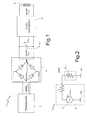
- Figure 1 is a schematic illustration by means of functional blocks of an energy-scavenging system of a known type.
- the energy-scavenging system 1 of Figure 1 comprises: a transducer 2, for example of an electromagnetic or piezoelectric type, subject during use to environmental mechanical vibrations and configured for converting mechanical energy into electrical energy, typically into AC voltages; a scavenging interface 4, for example comprising a diode-bridge rectifier circuit (also known as Graetz bridge), configured for receiving at input the AC signal generated by the transducer 2 and for supplying at output a DC signal for charging a capacitor 5 connected on the output of the rectifier circuit 4; and a DC-DC converter 6, connected to the capacitor 5 to receive at input the electrical energy stored by the capacitor 5 and supply it to an electrical load 8.
- the capacitor 5 has hence the function of element for storage of energy, which is made available, when required, to the electrical load 8 for operation of the latter.
- ⁇ TRANSD is the efficiency of the transducer 2, indicating the amount of energy available in the environment that is effectively converted, by the transducer 2, into electrical energy
- ⁇ SCAV is the efficiency of the scavenging interface 4, indicating the energy consumed by the scavenging interface 4 and the factor ⁇ COUPLE of matching between the transducer 2 and the scavenging interface 4 (indicating the impedance matching between the transducer 2 and the scavenging interface 4)
- ⁇ DCDC is the efficiency of the DC-DC converter 6.
- the transducer 2 can be represented schematically, in this context, as a voltage generator 3 provided with a resistance R S of its own.
- the power at input to the scavenging interface 4 is lower than the maximum power available P TRANSD MAX .
- P LOAD P DCDC ⁇ ⁇ DCDC
- P DCDC the power received at input by the DC-DC converter 8, in this case coinciding with P SCAV
- P LOAD is the power required by the electrical load.
- the efficiency of the system 1 of Figure 1 is markedly dependent upon the signal generated by the transducer 2.
- the efficiency drops rapidly to the zero value (i.e., the system 1 is unable to harvest environmental energy) when the amplitude of the signal of the transducer (signal V TRANSD ) assumes a value lower, in absolute value, than V OUT +2V TH_D , where V OUT is the voltage stored on the capacitor 5, and V TH_D is the threshold voltage of the diodes that form the scavenging interface 4.
- V OUT the voltage stored on the capacitor 5
- V TH_D is the threshold voltage of the diodes that form the scavenging interface 4.
- E max 0.5 ⁇ C OUT ⁇ (V TRANSD MAX - 2V TH_D ) 2 .
- V TRANSD the amplitude of the signal V TRANSD of the transducer 2 is lower than twice the threshold voltage V TH_D of the diodes of the rectifier of the scavenging interface 4 (i.e., V TRANSD ⁇ 2V TH_D ), then the efficiency of the system 1 is zero, the voltage stored on the output capacitor 5 is zero, the environmental energy is not harvested, and the electrical load 8 is not supplied.
- the aim of the present invention is to provide an enhanced-efficiency energy-scavenging interface, a method for operating the energy-scavenging interface, an energy-scavenging system comprising the energy-scavenging interface, and an apparatus comprising the energy-scavenging system that will enable the aforementioned problems and disadvantages to be overcome, and in particular that will present a high efficiency.
- an enhanced-efficiency energy-scavenging interface a method for operating the energy-scavenging interface, an energy-scavenging system comprising the energy-scavenging interface, and an apparatus comprising the energy-scavenging system are consequently provided as defined in the annexed claims.
- the energy-scavenging interface (in particular, having the configuration of a rectifier circuit) according to the present invention can be connected between an input signal source (in particular, a variable voltage signal) and an electrical load (with the possible interposition of a DC-DC converter designed to supply to the electrical load a voltage signal having a level of voltage accepted by the electrical load).
- the energy-scavenging interface comprises, according to an embodiment of the present invention, a first switch and a third switch, set in series, connected between the input terminal of the interface and an output terminal of the interface, which is set at constant voltage.
- the interface further comprises a second switch and a fourth switch, set in series, connected between the input terminal of the interface and the output terminal of the interface on which the energy is harvested.
- the energy-scavenging interface further comprises a control logic, coupled to the control terminals of the first and second switches, configured for controlling the first and second switches in off/on state by means of an appropriate control signal.
- the energy-scavenging interface moreover comprises a further third switch and fourth switch, each having a control terminal, and connected in series to the first and second switches, respectively.
- a capacitor for storing the power transferred at output of the scavenging interface.
- an electrical load which is supplied by means of the energy stored in the capacitor.
- a DC-DC converter of a buck, boost, or buck/boost type.
- the first and third switches are closed, and the energy-scavenging interface stores electrical energy in a storage element coupled to the first and third switches; the second switch is, instead, controlled in off-state so that the capacitor is not charged.
- the storage element In a second operating condition, the storage element is electrically coupled to the capacitor by opening the first switch and closing the second switch.
- the capacitor is charged by means of the electrical energy previously stored in the first operating condition.
- Passage from the first operating condition to the second operating condition, and vice versa, is cyclic.
- the energy-scavenging interface according to the present invention is described in detail with reference to a preferred application thereof, in particular as rectifier circuit of an energy-scavenging system set between a voltage source and a storage element and/or electrical load.
- the energy-scavenging interface further comprises a current-measuring and generating device coupled to conduction terminals of the third switch for detecting the current that flows, in use, through the third switch (and, consequently, also through the first switch).
- the current-measuring and generating device is moreover configured for generating a scaled copy of the current that flows through the third switch.
- generation of the scaled copy of the current is obtained by driving a further switch with a shape factor W/L reduced by an amount F with respect to the shape factor W/L of the third switch.
- the current that flows in said switch with shape factor W/L scaled by the amount F is hence F times less than the current that flows in the first and third transistors in the first operating condition.
- Figure 3a shows an energy-scavenging system 20 comprising a rectifier circuit 24, according to one embodiment of the present invention.
- the energy-scavenging system 20 comprises: a transducer 22 (similar to the transducer 2 of Figure 1 ) including output terminals 22', 22" of its own; the rectifier circuit 24, including a first input terminal 25' and a second input terminal 25", which are electrically coupled, respectively, to the output terminals 22', 22" of the transducer 22, and a first output terminal 26' and a second output terminal 26"; and a storage element 27, for example a capacitor, connected between the first and second output terminals 26', 26" of the rectifier circuit 24, and configured for storing electric charge supplied at output from the rectifier circuit 24.
- the second output terminal 26" is, according to an embodiment of the present invention, a terminal at reference voltage, for example at ground voltage GND, for instance, approximately 0 V. Other reference voltages may be used.
- the transducer 22 is, for example, an electromagnetic transducer, and is represented schematically so as to include a voltage generator 22a, designed to supply a voltage V TRANSD , an inductor 22b (typical of the electromagnetic transducer) having an inductance L S , and a resistor 22c having a resistance R S and connected in series to the inductor 22b.
- an electrical load 28 designed to be supplied by the charge stored in the storage element 27 or via a converter, for example, a DC-DC converter (not illustrated in the figure) if the electrical load requires a voltage value different from the one generated at output by the rectifier circuit 24.
- HV high-voltage
- LV low-voltage
- the switches 30a and 30b are, for example, n-channel field-effect transistors (FETs).
- the HV switch 30a is a device that is able to withstand high voltages.
- the HV switch 30a is a DMOS transistor that is able to operate with gate-to-drain voltages (V GD ) and drain-to-source voltages (V DS ) in the 30-50 V range, for example 40 V.
- the LV switch 30b is a low-voltage device.
- the LV switch 30b is a CMOS transistor that is able to operate with gate-to-source voltages (V GS ) in the 1-5 V range, in particular 2.5-3.6 V, for example 3.3 V.
- V GS gate-to-source voltages
- Other technologies for low-voltage transistors envisage slightly higher operating voltages, for example in the region of 4-5 V.
- V max_th a maximum tolerated voltage value at the first output terminal 26'(depending, for example, upon the characteristics of the capacitor 27 and/or of the load 28)
- high voltages gate-to-drain voltages (V GD ) and drain-to-source voltages (V DS ) of the respective transistor close to, but not higher than, said maximum tolerated voltage value (V max_th ).
- low voltages is, instead, understood gate-to-source voltages V GS of the respective transistor.
- a low-voltage (LV) switch 36b and a high-voltage (HV) switch 36a Connected in series with respect to one another between the first input terminal 25' and the first output terminal 26' are a low-voltage (LV) switch 36b and a high-voltage (HV) switch 36a, in particular of a voltage-controlled type.
- the switches 36b and 36a are, for example, n-channel FETs.
- the HV switch 36a is of the same type as the HV switch 30a, that is able to withstand high voltages
- the LV switch 36b is of the same type as the LV switch 30b, for low voltages.
- the HV switch 36a has the function of guaranteeing high voltages on the output terminal 26" of the rectifier circuit 24 Moreover, the rectifier circuit 24 further comprises: a high-voltage (HV) switch 31a and a low-voltage (LV) switch 31b, which are connected in series together and are electrically coupled between the second input terminal 25" and the second output terminal 26" of the rectifier circuit 24; and a high-voltage (HV) switch 38a and a low-voltage (LV) switch 38b, connected in series together and connected between the second input terminal 25" and the first output terminal 26'.
- HV high-voltage
- LV low-voltage
- the switches 31a and 31b are similar (and specular from a circuit standpoint) to the switches 30a and 30b, and such that the HV switch 31a is a device that is able to withstand high gate-to-drain and drain-to-source voltages (for example, 30-50 V, in particular 40 V), whereas the LV switch 31b is a low-voltage device, for example a CMOS, that is able to withstand low gate-to-source voltages (for example, 1-5 V, in particular 2.5-3.6 V, still more in particular 3.3 V).
- CMOS low-voltage device
- Other technologies for low-voltage transistors envisage slightly higher operating voltages, for example in the region of 4-5 V.
- the switches 38a and 38b are similar (and specular from a circuit standpoint) to the switches 36a and 36b, respectively, and such that the HV switch 38a is a device that is able to withstand high voltages, whereas the LV switch 38b is a low-voltage device, in a way similar to what has already been described with reference to the switches 36a and 36b, respectively.
- HV switches 30a, 36a, 31a, 38a will be referred to as in what follows, respectively, as high-voltage (HV) transistors 30a, 36a, 31a, 38a without this implying any loss of generality
- the low-voltage (LV) switches 30b, 36b , 31b, 38b will be referred to as in what follows, respectively, as low-voltage (LV) transistors 30b, 36b, 31b, 38b, without this implying any loss of generality.
- transistor closed will be meant in what follows a transistor biased in such a way as to enable conduction of electric current between its source and drain terminals, i.e., configured for behaving as a closed switch
- transistor open will be meant in what follows a transistor biased in such a way as not to enable conduction of electric current between its source and drain terminals, i.e., configured for behaving as an open or inhibited switch.
- FIG 3b shows the energy-scavenging system 20 of Figure 3a in which the switches have been replaced by respective transistors.
- Each transistor is moreover represented with its own internal diode (parasitic diode).
- the drain terminal D of the HV transistor 30a is connected to the first input terminal 25' of the rectifier circuit 24, whilst the source terminal S of the HV transistor 30a is connected to the drain terminal D of the LV transistor 30b; the source terminal S of the LV transistor 30b is, instead, connected to the second output terminal 26" of the rectifier circuit 24.
- the transistors 30a and 30b are effectively connected in series together between the input 25' and the output 26" of the rectifier circuit 24.
- the drain terminal D of the HV transistor 36a is connected to the first output terminal 26' of the rectifier circuit 24, and the source terminal S of the HV transistor 36a is connected to the drain terminal D of the LV transistor 36b; the source terminal S of the LV transistor is connected to the first input terminal 25' of the rectifier circuit 24.
- the HV transistor 36a and the LV transistor 36b are effectively connected in series together between the input 25' and the output 26' of the rectifier circuit 24.
- HV transistor 31a and the LV transistor 31b are connected between the second input terminal 25" and the second output terminal 26" of the rectifier circuit 24 so that the source terminal S of the LV transistor 31b is connected to the second output terminal 26", the drain terminal D of the HV transistor 31a is connected to the second input terminal 25", and the remaining drain terminal D of the LV transistor 31b and source terminal S of the HV transistor 31a are connected together.
- the HV transistor 38a and the LV transistor 38b are connected between the second input terminal 25" and the first output terminal 26' in such a way that the source terminal S of the LV transistor 38b is connected to the second input terminal 25", the drain terminal D of the HV transistor 38a is connected to the first output terminal 26', and the remaining drain terminal D of the LV transistor 38b and source terminal S of the HV transistor 38a are connected together.
- the voltage rectification is carried out by driving appropriately the HV transistors 30a and 36a, keeping the LV transistors 30b and 36b in the closed state.
- the transistors 31a, 31b, and 38b are in a closed state, whereas the transistor 38a is in an open state.
- the voltage rectification is carried out by driving appropriately the HV transistors 31a and 38a, keeping the LV transistors 31b and 38b in the closed state.
- the transistors 30a, 30b, and 36b are kept in a closed open state, whereas the transistor 36a is open.
- the rectifier circuit 24 further comprises a control circuit and a control logic, designated in Figure 3a or Figure 3b by the reference numbers 60 and 70, and described in greater detail with reference to Figures 8 and 9 .
- the control logic 60 implements the steps of the method of Figure 13 .
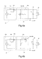
- the HV transistor 30a and the LV transistor 30b are kept closed for at least a time interval T DELAY so as to store energy in the inductor 22b (situation shown schematically in Figure 4a ).
- T DELAY time interval
- at least one between the transistors 36a and 36b is kept in an open state (according to one embodiment, the transistor 36b is always kept in the closed state).
- the transistor 31a is controlled in the closed state
- the transistor 31b is kept in the closed state
- the transistor 38a is controlled in the open state.
- the input signal V IN is, as has been said, a variable signal, i.e., a signal having a time-variable polarity.
- V IN a variable signal
- a signal having a time-variable polarity For negative polarities of V IN , what has been described with reference to Figures 4a and 4b in any case applies by controlling the transistors 31a, 31b, 38a and 38b in a similar way. The steps for control of these transistors are not described herein for reasons of brevity, but they will be apparent to any person skilled in the sector, on the basis of what has been described so far.
- the LV transistors 30b and 36b are always kept closed, and the control logic 60 drives in an open/closed state just the HV transistors 30a and 36a.
- the control logic 60 drives in an open/closed state just the HV transistors 31a and 38a, whereas the LV transistors 31b and 38b are always kept closed.
- FIG. 3b This situation is represented schematically in Figure 3b by showing voltage generators, designed to generate a voltage V DD , coupled to the control terminals G of the LV transistors 30b, 31b, 36b, and 38b.
- the voltage V DD has a value such as to drive into the closed state the LV transistors 30b, 31b, 36b, and 38b.
- control logic 60 can drive actively into an open/closed state both of the transistors 36a and 36b, and both of the transistors 38a and 38b, without thereby interfering with the steps of charging of the inductor 22b and supply of the capacitor 27/load 28 described previously.
- Figure 4a shows a circuit equivalent to the circuit of Figure 3a or Figure 3b , for positive half-waves of the input voltage V IN .
- the HV transistor 36a is open and the LV transistor 36b is closed.
- the transistors 30a and 30b are closed. In this operating condition, the transistors 30a and 30b are ideally replaced by respective resistors which have an on-state resistance R HV ON and R LV ON , respectively.
- the current I L that flows in the inductor 22b is equal to the current I ON that traverses the transistors 30a and 30b in the on state.
- the value of the current I L increases up to a maximum value, or peak value, I P (see the graph of Figure 5a ).
- the starting instant t 0 is 0 ⁇ s.
- the time interval T DELAY is the interval elapsing between the instant of closing of the HV transistor 30a (at time to) and the instant of opening of the HV transistor 30a and closing of the transistor 36a (at time t c ). It is evident that, prior to closing of the HV transistor 36a it is expedient to open the HV transistor 30a so as to prevent phenomena of cross conduction and dissipation of power from the output capacitor 27 to ground GND.
- threshold current I TH is chosen on the basis of the peak values of current I p that are reached, and/or on the basis of the application of the rectifier circuit 24. These values depend upon the characteristics of the transducer 22 and upon the environmental stresses to which the transducer 22 is subject. In particular, the value of threshold current I TH is chosen much lower than the peak value I p that is expected to be reached in the application in which the rectifier circuit 24 is used. For example, assuming that peak values I p are reached of approximately 150 mA, the threshold I TH can be chosen as comprised between approximately 5 and 10 mA. It is pointed out that the choice of a threshold current I TH too close to the peak value I p entails a low efficiency. In fact, according to what has been described, current is transferred at output only when the threshold I TH is exceeded. All the portions of signal V TRANSD that generate a current with peak value I p ⁇ I TH do not give contribution of charge transferred at output.
- the HV transistor 30a is opened, and the HV transistor 36a is closed (as has been said, preferably respecting an guard interval to prevent cross conduction); the current I L that flows from the inductor 22b to the output 26' of the rectifier 24 is the current I OUT that charges the capacitor 27.
- the current in the inductor 22b decreases with a constant slope until it reaches the pre-defined value I OFF
- I OFF is a constant value, given by I p /K, with K constant greater than 1 (chosen as explained hereinafter), we obtain the following formula for the peak value I P :
- I P V TRANSD R 1 + R S ⁇ 1 - e - T DELAY ⁇ 1 - 1 K ⁇ e - T DELAY ⁇
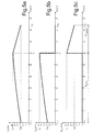
- Figure 5a shows the plot of the current I L in time t ( ⁇ s).
- the curve of the current I L reaches the peak value I P at the instant t c , when the HV transistor 30a is opened (see Figure 5b ) and the HV transistor 36a is closed.
- Figure 5b shows, using the same time scale as that of Figure 5a , the plot of the current I ON that flows through the HV transistor 30a during the step of Figure 4a of charging of the inductor 22b.
- the current I ON presents the same evolution as the current I L ; at the instant t c , the HV transistor 30a is opened and, consequently, the current I ON drops to zero.
- Figure 5c shows, using the same time scale as that of Figures 5a and 5b , the plot of the output current I OUT .
- the current I OUT remains at a zero value in the time interval t 0 -t c , and then reaches the peak value I P at the instant t c , when the capacitor 27 is electrically coupled to the inductor 22b. Then, between t c and t max (within the time interval T CHARGE ), the energy stored in the inductor 22b supplies and charges the capacitor 27.
- T CHARGE L S ⁇ I P - I OFF V OUT + R S + R ON ⁇ HV + R ON ⁇ LV ⁇ I P + I OFF 2 - V TRANSD
- the integral of the curve of I OUT ( Figure 5c ) between the time t c and the time t max indicates the charge Q CYCLE transferred between the input and the output of the rectifier 24 in the time T CHARGE .
- the value of the power P CYCLE transferred at output in each cycle of charge/discharge of the inductor 22b should be maximized.
- the power P CYCLE is a function of the design parameters T DELAY and K, and of the external variables V TRANSD (voltage of the transducer, which is not predictable) and V OUT (voltage on the capacitor 27, which is not predictable either). Maximizing the value of P CYCLE hence means finding the optimal values of T DELAY and K in such a way that the curve of P CYCLE reaches a maximum value, or a value close to the maximum value, or an optimal value that can be defined according to the particular application and design requirements.
- the curve of P CYCLE reaches an optimal value when the output of the transducer 22 and the input of the rectifier circuit 24 show the same impedance (namely, they are matched).
- the best matching efficiency ⁇ COUPLE between the transducer 22 and the rectifier circuit 24 is given by P CYCLE OPT /P TRANSD MAX , where P CYCLE OPT is the value of P CYCLE calculated with optimal values of T DELAY and K, and P TRANSD MAX is given by (V TRANSD ) 2 /4R s .
- Figure 6 shows the evolution of the matching efficiency ⁇ COUPLE as the values T DELAY and K vary.
- the graph of Figure 6 can be obtained easily starting from the expression of P CYCLE by varying the parameters T DELAY and K (fixing the values of the external variables V TRANSD and V OUT ).
- Corresponding to each value of ⁇ COUPLE is a pair of values T DELAY and K. It is thus possible to derive in an automatic way the pair of optimal values T DELAY and K to obtain a desired value of matching efficiency ⁇ COUPLE .
- the darker areas are those in which the value of matching efficiency ⁇ COUPLE is higher; instead, the lighter areas are those in which the value of matching efficiency ⁇ COUPLE is lower (low values of T DELAY and high values of K, or high values of T DELAY and low values of K).
- Figure 7 shows profiles of current I L in the inductor 22b as pairs of values of T DELAY and K vary, and with reference to a optimal ideal current value I L OPT (condition of matched load in which the matching efficiency is maximum).
- the values of peak current I p reached by the current I L according to the curve 65 are high, and the impedance matching between the transducer 22 and the rectifier circuit 24 other than optimal, causing a relatively low matching efficiency ⁇ COUPLE ( ⁇ COUPLE ⁇ 72.3%).
- the matching efficiency ⁇ COUPLE is still higher than in the case of the curve 67 (approximately 99.5%), but with the disadvantage that the driving frequency of the HV transistors 30a and 36a (or HV transistors 31a and 38a) is excessively high, thus causing an excessive current consumption by the rectifier circuit 24, with consequent reduction in the efficiency factor ⁇ SCAV not sufficiently compensated for by the increase in the value of matching efficiency ⁇ COUPLE .
- FIG 8 shows, by means of functional blocks, a control circuit 70 for driving the HV transistor 30a and the HV transistor 36a in order to implement the operating conditions of Figures 4a and 4b .
- the control circuit 70 operates, in particular, for positive half-waves (V IN + ) of the input signal V IN .
- the LV transistor 36b is biased with a gate-to-source voltage (V GS ) equal to V DD , whereas the LV transistor 30b is biased at a constant voltage V DD , in such a way as to be kept always in the on state.
- the value of the voltage V DD is hence chosen on the basis of the characteristics of the transistors 30b and 36b, in such a way as to drive them into the on state.
- control circuit 70 comprises a first current detector 72, coupled between the source terminal S and the drain terminal D of the LV transistor 30b, for detecting (during the step of Figure 4a ) when the current I ON that flows through the LV transistor 30b (and, consequently, also through the HV transistor 30a) exceeds the threshold I TH .
- the current detector 72 has also the function of generating, in the step of Figure 4a , a scaled copy of the current that flows in the LV transistor 30b, as illustrated more fully in what follows.
- Figure 9 shows in greater detail the first current detector 72, according to an embodiment.
- a first portion of the current detector 72 comprises a comparator 86 configured for receiving at input the voltage signals present on the source terminal S and on the drain terminal D of the LV transistor 30b and generating at output a digital signal that assumes a low logic level when I ON ⁇ I TH and a high logic level when I ON ⁇ I TH (or vice versa).
- the signal at output from the comparator 86 is supplied to the control logic 60, which, once the time interval T DELAY has elapsed, opens the HV transistor 30a.
- the duration of the time interval T DELAY can be determined either by the control logic 60 or by the comparator 86 belonging to the current detector 72.
- the signal at output from the comparator 86 assumes a high logic level when I ON ⁇ I TH and t ⁇ T DELAY , and the control logic 60 opens the HV transistor 30a at the rising edge of the digital signal generated by the comparator 86.
- a second portion of the current detector 72 comprises a negative-feedback loop including an amplifier 89 that controls the current that flows on an output branch 90 of the current detector 72 by acting on the control terminal of a transistor 91 belonging to the output branch 90 (i.e., by opening/closing the transistor 91).
- the negative feedback ensures that the voltage on the inverting input of the amplifier 89 is always equal to the voltage present on the non-inverting input of the amplifier 89.
- the output branch 90 moreover comprises a further transistor 92 having dimensions (understood as W/L ratio) that are smaller by a factor F than the respective dimensions (understood as W/L ratio) of the LV transistor 36b.
- the control circuit 70 further comprises a second current detector 74, coupled to the source terminal S and to the drain terminal D of the LV transistor 36b.
- the second current detector 74 is similar to the first current detector 72 and is configured for detecting the value of current that flows through the LV transistor 36b (and, consequently, through the HV transistor 36a) during the operating step of Figure 4b .
- the output signal of the second current detector 74, indicating the current value I OUT is supplied at input to the control logic 60.
- the control circuit 70 further comprises a first driving device 76 and a second driving device 78, coupled, respectively, between the control logic 60 and the control terminal G of the HV transistor 30a and of the HV transistor 36a.
- the first driving device 76 and the second driving device 78 are, in themselves, of a known type, and are designed to drive into an open/closed state the transistors 30a, 36a on the basis of a control signal received from the control logic 60.
- the control logic 60 drives, via the first driving device 76, the HV transistor 30a into the closed state and, via the second driving device 78, the HV transistor 36a into an open state.
- control logic 60 monitors, on the basis of the signal received from the second current detector 74, the value of the current I OUT for controlling passage from the current operating condition (of supply of the load, Figure 4b ) to the operating condition of storage of energy in the inductor 22b ( Figure 4a ), as soon as the current I OUT reaches the value I OFF .
- the control circuit 70 further comprises a first voltage detector 80 and a second voltage detector 82, which are, respectively, coupled between the control terminal G and the source S of the HV transistor 30a and of the HV transistor 36a.
- the first voltage detector 80 detects the voltage present between the control terminal G of the HV transistor 30a and the source terminal S of the LV transistor 30b (in this case, corresponding to the reference terminal GND) and generates an output signal indicating said voltage.
- the output signal generated by the first voltage detector 80 is supplied to the control logic 60.
- the second voltage detector 82 detects the voltage present between the control terminal G of the HV transistor 36a and the source terminal S of the LV transistor 36b (in this case, corresponding to the input node 25') and generates an output signal indicating said voltage.
- the control logic 60 knows the state, whether on or off, of the HV transistors 30a and 36a, and controls passage from the operating condition of Figure 4a to the operating condition of Figure 4b (and vice versa) inserting appropriate dead times between opening (closing) of the HV transistor 30a and closing (opening) of the HV transistor 36a. There are thus prevented phenomena of cross conduction and direct connection between the first output terminal 26' (to which the capacitor 27/load 28 is coupled) and the ground-reference terminal GND.
- Figure 9 shows, according to an embodiment of the present invention, the first current detector 72.
- the first current detector 72 further comprises means designed to store the peak value I p of the current I ON that traverses, in use, the HV transistor 30a.
- the first current detector 72 further comprises a transistor 87 having a drain terminal common to the drain terminal of the LV transistor 30b, and its source terminal coupled to a capacitor 88 (the second terminal of the capacitor 88 is connected to the reference voltage GND).
- the control terminal G of the transistor 87 is connected to the control terminal G of the HV transistor 30a. In this way, the HV transistor 30a and the transistor 87 are driven into an open/closed state by one and the same signal V GATE_LS .
- the HV transistor 30a is closed (the signal V GATE_LS has a high value and drives the HV transistor 30a into the closed state).
- the transistor 87 is closed.
- the capacitor 88 is consequently charged to the voltage present on the first input terminal 25' of the rectifier circuit 24 (in Figure 9 the voltage across the capacitor 88 is designated by V C_SAMPLE ).
- the first current detector 72 moreover comprises a further comparator 89 and a branch 90 including a transistor 91 and a transistor 92 connected in series together between a terminal 90' and the reference terminal GND.
- the transistor 91 has its own source terminal coupled to the drain terminal of the transistor 92; moreover, the transistor 92 has its own control terminal G connected to a constant-voltage supply terminal V DD .
- the transistor 92 is a low-voltage transistor, for example a CMOS.
- the transistor 92 is able to operate with gate-to-source voltages in the 1-5 V range, in particular 2.5V-3.6 V, for example 3.3 V.
- the transistor 92 is of the same type as the LV transistor 30b, but is sized so the transistor 92 has dimensions (measured in terms of shape factor W/L, width/length) F times smaller than the LV transistor 30b and is designed to conduct a current F times lower than the value assumed by I ON (current that flows through the LV transistor 30b).
- the LV transistor 30b and the transistor 92 moreover have their respective control terminals connected together and biased at the voltage V DD .
- the negative feedback, provided by means of the comparator 89 and the transistor 91, ensures that the drain voltages of the transistors 30b and 92 are identical.
- both of the transistors 30b and 92 are low-voltage transistors (e.g., CMOSs) they provide excellent matching properties so that the factor F is affected to a minimal extent by problems of mismatch between the transistors 30b and 92 (as, instead, the case if the transistor 30b and 92 were high-voltage transistors). This enables a scaled copy of the peak current I P to be obtained that is stable and with has a riproducible value.
- the comparator 89 is connected to the source terminal of the transistor 87, and, when the transistor 87 is closed, it receives at input (on the non-inverting terminal) the voltage of the drain terminal of the LV transistor 30b, and at input (on the inverting terminal) the signal present on the drain terminal of the transistor 92 and source terminal of the transistor 91; the output of the comparator 89 is coupled to the control terminal G of the transistor 91.
- the transistor 91 is always closed; the comparator 89 biases the control terminal of the transistor 91 in such a way that on the branch 90 there flows the current I ON /F, as desired.
- the negative feedback provided by the comparator 89 ensures that the signal at input to the non-inverting terminal of the comparator 89 and the signal at input to the inverting terminal of the comparator 89 are equal, so that the LV transistor 30b and the transistor 92 will have the same source-to-drain and source-to-gate voltages.
- the capacitor 88 ensures maintenance of the voltage V C_SAMPLE across it, guaranteeing an input signal that is substantially constant (but for the losses of the capacitor 88) on the non-inverting input of the comparator 89.
- This makes it possible to keep unaltered the generation of the current I ON /F on the output branch 90 of the first current detector 72 during the step of Figure 4b (in this step, the current I ON has reached the peak value I P , and consequently flowing in the output branch 90 of the first current detector 72 is a current I P /F).
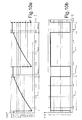
- Figure 10a shows graphically the time plot of the voltage on the drain terminal of the LV transistor 30b and of the voltage signal V C_SAMPLE across the capacitor 88. These signals have the same evolution and coincide with one another in Figure 10a.
- Figure 10b shows the time plot of the signal V GATE_LS applied to the control terminals of the HV transistor 30a and of the transistor 87.
- V C_SAMPLE drops to the value I OFF ⁇ (R HV ON +R LV ON ) where R HV ON and R LV ON are, respectively, the on-state resistances of the HV transistor 30a and the LV transistor 30b.
- FIG 11 shows, in greater detail, the second current detector 74.
- the second current detector 74 of Figure 11 comprises a transistor 97, having a source terminal S connected to the first input terminal 25' of the rectifier circuit 24, a control terminal G connected to the control terminal G of the LV transistor 36b, and a drain terminal D.
- a resistor 98 is shown representing the on-state electrical resistance R ON_DMY of the transistor 97.
- the LV transistor 36b and the HV transistor 36a are shown with their own respective on-state electrical resistances R ON ⁇ LV and R ON ⁇ HV connected in parallel (resistors 96 and 95).
- the second current detector 74 further comprises a comparator 99, having an inverting terminal connected between the drain terminal of the LV transistor 36b and the source terminal of the HV transistor 36a (to receive an intermediate output signal V OUT_INT ), and a non-inverting terminal connected to the drain terminal of the transistor 97 (to receive an intermediate reference signal V REF_INT ).
- the transistor 97 is a replica, scaled by a factor J, of the LV transistor 36b. Consequently, the transistors 36b and 97 are sized in such a way that the transistor 97 has dimensions (measured in terms of shape factor W/L, width/length) that are J times smaller than those of the LV transistor 36b and is designed to conduct a current F times lower than the value assumed by I ON (i.e., I ON /F) during the step of Figure 4a , and a current F times lower than the peak value I P (i.e., I P /F) during the step of Figure 4b .
- V REF_INT V IN + - J ⁇ R ON_DMY ⁇ I P / F
- V OUT_INT V IN + - R ON ⁇ LV ⁇ I OUT
- I OUT is the current that flows through the transistors 36b and 36a when they are in the on state.
- both of the transistors 36b and 97 are low-voltage transistors (e.g., CMOSs) of the same type and hence they guarantee excellent matching properties, such that the factor J is affected to a minimal extent by problems of mismatch between the transistors 36b and 97 (as, instead, would be the case if both of the transistors were high-voltage transistors).
- Stabilizing J around a value corresponds desired to stabilizing the value of K around the value chosen.
- the parameter K has a minimal spread around the chosen and desired value.
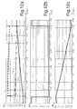
- Figures 12a-12c show, using one and the same time scale: the plot of the signals V IN + , V REF_INT , V OUT ( Figure 12a ); the plot of the signal V OUT_COMP generated at output from the comparator 99 ( Figure 12b ); and the plot of the current signal I L ( Figure 12c ).
- Figure 12c shows the current I L , in particular during the time interval T CHARGE (operating condition of Figure 4b ).
- the current I L I OUT decreases from a maximum value I P to a value minimum I OFF , supplying the capacitor 27/load 28.
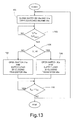
- the control logic 60 implements the method of control of the HV transistors 30a, 36a, 31a, and 38a described previously and shown schematically in Figure 13 , by means of a flowchart.
- step 100 the HV transistors 30a and 31a are closed.
- the HV transistors 36a and 38 instead, are opened.
- the LV transistors 30b, 31b, 36b and 38b are always assumed as being in the closed state (situation of Figure 3b ).
- the current value I L I ON is monitored (step 102) for detecting whether it reaches (or exceeds) the required threshold value I TH .
- the control logic 60 monitors the time interval T DELAY .
- the time to of start of the time interval T DELAY corresponds to the closing instant of the HV transistors 30a, 31a, according to step 100.
- step 104 a check is made to verify whether the input voltage V IN has a positive polarity or a negative polarity. This operation can be carried out by means of the comparator 86, which receives at input the signal V IN + .
- control passes to step 106 (output YES from step 104), where the HV transistor 30a, and possibly the LV transistor 30b, are opened to supply the capacitor 27/load 28 via the HV transistors 36a and LV switch 36b.
- control passes, instead, to step 108 (output NO from the step 104), where the capacitor 27/load 28 is supplied via the LV transistor 38b and HV transistor 38a.
- step 110 the control logic 60 monitors the value of current I OUT that flows through the LV transistor 36b (or the LV transistor 38b according to the polarity of the input voltage V IN ) towards the output of the rectifier 24 for detecting whether the current I OUT assumes a value equal to I OFF .
- the control logic 60 keeps the system 20 in the step of charging of the capacitor 27/supply of the load 28.
- the steps 100-104 are executed, as described with reference to Figures 5a-5c , in a time interval equal to at least T DELAY until the current in the inductor reaches the threshold I TH whereas the steps 106-110 are executed within the time interval T CHARGE .
- the control logic 60 is, for example, a microcontroller configured for driving the HV transistors 30a, 31a, 36a, and 38a in order to carry out the steps of the method of Figure 13 .
- FIG 14 shows a vehicle 200 comprising the energy-scavenging system 20 of Figure 3 .
- the vehicle 200 is, in particular, a motor vehicle. It is evident, however, that the energy-scavenging system 20 can be used in any vehicle 200 or in systems or apparatuses different from a vehicle. In particular, the energy-scavenging system 20 can find application in generic systems in which it is desirable to harvest, store, and use environmental energy, in particular by means of conversion of mechanical energy into electrical energy.
- the vehicle 200 comprises one or more transducers 22 coupled in a known way to a portion of the vehicle 200 that is subject to mechanical stresses and/or vibrations, for converting said mechanical stresses and/or vibrations into electric current.
- the energy-scavenging system 20 is connected to one or more electrical loads 28a, ..., 28n, for example via interposition of a DC-DC converter.
- the electrical loads 28a, ..., 28n comprise TPM (tyre-parameter monitoring) sensors 250 for monitoring parameters of tyres 202.
- the TPM sensors 250 are coupled to an internal portion of the tyres 202 of the vehicle 200.
- the transducers 22 are coupled to an internal portion of the tyres 202.
- the stress of the transducers 22 when the vehicle 200 is travelling causes production of an electric current/voltage signal at output from the transducer 22 by means of conversion of the mechanical energy into electrical energy.
- the electrical energy thus produced is stored, as has been described previously, in the storage element 27 and supplied, via the DC-DC converter that may possibly be present, to the TPM sensors 250.
- the energy-scavenging system 20, comprising one or more transducers, and the TPM sensors 250, are glued inside one or more tyres 202. Impact of the tyres 202 on the ground during motion of the vehicle 200 enables production of electrical energy.
- the energy-scavenging system 20 can be arranged in any other portion of the vehicle 200, and/or used for supplying an electrical load other than or additional to the TPM sensors 250.
- the energy-scavenging system 20 is the generation of electrical energy by exploiting the mechanical energy produced by a person when he is walking or running.
- the energy-scavenging system 20 is set inside the shoes 300 of said person (for example, inside the sole) as shown schematically in Figure 15 .
- the parameter K has a highly riproducible value (minimum spread) so as to increase the performance, robustness and efficiency of the system 20, minimizing the mismatch between the positive and negative polarities of the signal of the transducer and preventing phenomena of reversal of the flow of current from the capacitor 27 to the input terminals 25', 25" of the rectifier circuit 24.
- the rectifier 24 since the duration of the time interval T DELAY is (typically) constant, the rectifier 24 operates at constant duty cycle of the signal of opening/closing of the first and second switches 30, 31. This enables values of efficiency ⁇ SCAV (efficiency of the rectifier 24, having the function of scavenging interface of the system 20) to be obtained that are particularly high (the present applicant has found efficiency values higher than 95% irrespective of the values assumed by V TRANSD and V OUT ).
- the scavenging efficiency is moreover high even when the amplitude of the signal V TRANSD of the transducer 22 is lower than the voltage value stored in the capacitor 27, overcoming a limitation of the diode-bridge rectifier architecture.
- the rectifier 24 exploits the inductor 22b inside the transducer 22, the scavenging efficiency is high even when the amplitude of the signal of the transducer is low.
- HV high-voltage
- the method described which envisages the choice of an optimal value of T DELAY and of K, enables implementation of an active control (of the mean value and of the ripple) of the current supplied by the transducer, and enables an optimal matching of impedance between the transducer 22 and the scavenging interface 24. This ensures an efficiency ⁇ SCAV of the scavenging interface 24b that is high irrespective of the velocity of rotation of the tyres 202 and of the conditions of storage of energy in the capacitor 27.
- the value of the interval T DELAY may be varied according to the particular application in which the rectifier 24 operates.
- the rectifier 24 thus finds use in systems other than the energy-scavenging system 20, i.e., ones based upon electromagnetic transducers of any type.
- the rectifier circuit 24 may be used with transducers of another type, by interposition of an appropriate circuit between the transducer and the rectifier circuit designed to provide a storage of energy similar to the inductor 22b.
- the rectifier 24 according to the present invention and the energy-scavenging system 20 are of a fully integrated type, and consequently require minimal space for installation.
- the scavenging interface 24 is hence able to harvest energy even when the power supplied by the transducer is very low.
- the rectifier circuit 24 may comprise a number of transistors different from the one described.
- the rectifier circuit 24 may be a half-wave rectifier, comprising only the switches that operate for positive polarity of the input signal V IN (i.e., the switches 30a, 30b, 36a, and 36b) or only the switches that operate for negative polarities of the input signal V IN (i.e., the switches 31a, 31b, 38a, and 38b).
- the use of a half-wave rectifier may be advantageous in the case where the input signal V IN is of a known type and comprises only positive (or negative) half-waves. Its use is, however, not recommended (even though it is possible) in energy-scavenging systems in so far as part of the input signal would be lost, at the expense of the efficiency of the system as a whole.
- the transducer/transducers may be chosen in the group comprising: electrochemical transducers (designed to convert chemical energy into an electrical signal), electromechanical transducers (designed to convert mechanical energy into an electrical signal), electroacoustic transducers (designed to convert pressure variations into an electrical signal), electromagnetic transducers (designed to convert a magnetic field into an electrical signal), photoelectric transducers (designed to convert light energy into an electrical signal), electrostatic transducers, thermoelectric transducers, piezoelectric transducers, thermoacoustic transducers, thermomagnetic transducers, thermoionic transducers.
- electrochemical transducers designed to convert chemical energy into an electrical signal
- electromechanical transducers designed to convert mechanical energy into an electrical signal
- electroacoustic transducers designed to convert pressure variations into an electrical signal
- electromagnetic transducers designed to convert a magnetic field into an electrical signal
- photoelectric transducers designed to convert light energy into an electrical signal
- electrostatic transducers thermoelectric transducers, piezoelectric transducers, thermoacous
Landscapes
- Engineering & Computer Science (AREA)
- Power Engineering (AREA)
- Dc-Dc Converters (AREA)
- Control Of Electric Motors In General (AREA)
- Electrotherapy Devices (AREA)
Description
- The present invention relates to an enhanced-efficiency energy-scavenging interface, to a method for operating the energy-scavenging interface, and to an energy-scavenging system comprising the energy-scavenging interface. In particular it regards an energy-scavenging interface including a rectifier circuit.
- The present invention moreover regards an apparatus (for example, a vehicle or an item of footwear) comprising the energy-scavenging system.
- As is known, systems for energy scavenging or energy harvesting from environmental energy sources have aroused and continue to arouse considerable interest in a wide range of fields of technology. Typically, energy-scavenging systems are designed to harvest, store, and transfer energy generated by mechanical sources to a generic load of an electrical type.
- Low-frequency vibrations, such as, for example, mechanical vibrations of disturbance in systems with moving parts, may be a valid source of energy. The mechanical energy is converted, by one or more purposely provided transducers (for example, piezoelectric or electromagnetic devices) into electrical energy, which can be used for supplying an electrical load. In this way, the electrical load does not require batteries or other supply systems that are cumbersome and have a poor resistance to mechanical stresses.
-
Figure 1 is a schematic illustration by means of functional blocks of an energy-scavenging system of a known type. - The energy-
scavenging system 1 ofFigure 1 comprises: atransducer 2, for example of an electromagnetic or piezoelectric type, subject during use to environmental mechanical vibrations and configured for converting mechanical energy into electrical energy, typically into AC voltages; ascavenging interface 4, for example comprising a diode-bridge rectifier circuit (also known as Graetz bridge), configured for receiving at input the AC signal generated by thetransducer 2 and for supplying at output a DC signal for charging acapacitor 5 connected on the output of therectifier circuit 4; and a DC-DC converter 6, connected to thecapacitor 5 to receive at input the electrical energy stored by thecapacitor 5 and supply it to anelectrical load 8. Thecapacitor 5 has hence the function of element for storage of energy, which is made available, when required, to theelectrical load 8 for operation of the latter. - The global efficiency ηTOT of the energy-
scavenging system 1 is given by
where: ηTRANSD is the efficiency of thetransducer 2, indicating the amount of energy available in the environment that is effectively converted, by thetransducer 2, into electrical energy; ηSCAV is the efficiency of thescavenging interface 4, indicating the energy consumed by thescavenging interface 4 and the factor ηCOUPLE of matching between thetransducer 2 and the scavenging interface 4 (indicating the impedance matching between thetransducer 2 and the scavenging interface 4); and ηDCDC is the efficiency of the DC-DC converter 6. - As is known, in order to supply to the load the maximum power available, the impedance of the load should be the same as that of the source. As shown in
Figure 2 , thetransducer 2 can be represented schematically, in this context, as avoltage generator 3 provided with a resistance RS of its own. The maximum power PTRANSD MAX that thetransducer 2 can supply at output can be defined as
where: VTRANSD is the voltage supplied by the equivalent voltage generator; and RLOAD is the equivalent electrical resistance on the output of the transducer 2 (or, likewise, the resistance seen at input to the scavenging interface 4), which takes into due account the equivalent resistance of thescavenging interface 4, of the DC-DC converter 6, and of theload 8. - On account of the impedance mismatch (RLOAD ≠ RS), the power at input to the
scavenging interface 4 is lower than the maximum power available PTRANSD MAX. - The power PSCAV is supplied at output by the
scavenging interface 4 and is given by
- The power required of the DC-
DC converter 6 for supplying theelectrical load 8 is given by
where PDCDC is the power received at input by the DC-DC converter 8, in this case coinciding with PSCAV, and PLOAD is the power required by the electrical load. - The efficiency of the
system 1 ofFigure 1 is markedly dependent upon the signal generated by thetransducer 2. The efficiency drops rapidly to the zero value (i.e., thesystem 1 is unable to harvest environmental energy) when the amplitude of the signal of the transducer (signal VTRANSD) assumes a value lower, in absolute value, than VOUT+2VTH_D, where VOUT is the voltage stored on thecapacitor 5, and VTH_D is the threshold voltage of the diodes that form thescavenging interface 4. As a consequence of this, the maximum energy that can be stored in thecapacitor 5 is limited to the value Emax=0.5·COUT·(VTRANSD MAX- 2VTH_D)2. If the amplitude of the signal VTRANSD of thetransducer 2 is lower than twice the threshold voltage VTH_D of the diodes of the rectifier of the scavenging interface 4 (i.e., VTRANSD<2VTH_D), then the efficiency of thesystem 1 is zero, the voltage stored on theoutput capacitor 5 is zero, the environmental energy is not harvested, and theelectrical load 8 is not supplied. - The aim of the present invention is to provide an enhanced-efficiency energy-scavenging interface, a method for operating the energy-scavenging interface, an energy-scavenging system comprising the energy-scavenging interface, and an apparatus comprising the energy-scavenging system that will enable the aforementioned problems and disadvantages to be overcome, and in particular that will present a high efficiency.
- According to the present invention an enhanced-efficiency energy-scavenging interface, a method for operating the energy-scavenging interface, an energy-scavenging system comprising the energy-scavenging interface, and an apparatus comprising the energy-scavenging system are consequently provided as defined in the annexed claims.
- For a better understanding of the present invention, preferred embodiments thereof are now described, purely by way of non-limiting example and with reference to the attached drawings, wherein:
-
Figure 1 shows an energy-scavenging system according to a known embodiment; -
Figure 2 shows a circuit equivalent to the energy-scavenging system ofFigure 1 ; -
Figures 3a and3b show an energy-scavenging system comprising a scavenging-interface circuit that can be operated according to the steps of the method ofFigure 13 , second respective embodiments of the present invention; -
Figures 4a and 4b show the energy-scavenging system ofFigure 3a or3b in respective operating conditions, that follow one another in time; -
Figures 5a-5c show, using one and the same time scale, the time plot of current signals of the energy-scavenging system ofFigure 3a orFigure 3b in the operating conditions ofFigures 4a and 4b ; -
Figure 6 shows the plot of the matching factor between the transducer and the scavenging-interface circuit ofFigures 3a ,3b , as the operating parameters vary; -
Figure 7 shows profiles of storage/discharge of current in the energy-scavenging system in the operating conditions ofFigures 4a and 4b ; -
Figure 8 shows a circuit for management and control of the scavenging-interface circuit ofFigures 3a ,3b that can be used for positive half-waves of the signal at input to the scavenging-interface circuit; -
Figure 9 shows, in greater detail, a portion of the management and control circuit ofFigure 8 ; -
Figures 10a and 10b illustrate, using one and the same time scale, the time plot of current signals in the circuit ofFigure 8 , in particular for showing a step of passage between the operating condition ofFigure 4a and the operating condition ofFigure 4b ; -
Figure 11 shows, in greater detail, a further portion of the management and control circuit ofFigure 8 ; -
Figures 12a to 12c show, using one and the same time scale, the time plot of current signals in the circuit ofFigure 11 ; -
Figure 13 shows, using a flowchart, steps of a control method for driving the energy-scavenging system ofFigure 3a orFigure 3b , according to one embodiment of the present invention; -
Figure 14 shows a vehicle comprising the energy-scavenging system ofFigure 3a orFigure 3b ; and -
Figure 15 shows an item of footwear comprising the energy-scavenging system ofFigure 3a orFigure 3b . - The energy-scavenging interface (in particular, having the configuration of a rectifier circuit) according to the present invention can be connected between an input signal source (in particular, a variable voltage signal) and an electrical load (with the possible interposition of a DC-DC converter designed to supply to the electrical load a voltage signal having a level of voltage accepted by the electrical load). The energy-scavenging interface comprises, according to an embodiment of the present invention, a first switch and a third switch, set in series, connected between the input terminal of the interface and an output terminal of the interface, which is set at constant voltage. The interface further comprises a second switch and a fourth switch, set in series, connected between the input terminal of the interface and the output terminal of the interface on which the energy is harvested. The energy-scavenging interface further comprises a control logic, coupled to the control terminals of the first and second switches, configured for controlling the first and second switches in off/on state by means of an appropriate control signal.
- The energy-scavenging interface moreover comprises a further third switch and fourth switch, each having a control terminal, and connected in series to the first and second switches, respectively.
- Present on the output of the energy-scavenging interface is a capacitor for storing the power transferred at output of the scavenging interface. In parallel to the capacitor there may be present an electrical load, which is supplied by means of the energy stored in the capacitor. As has already been said, between the capacitor and the electrical load there can be set a DC-DC converter, of a buck, boost, or buck/boost type.
- In a first operating condition, the first and third switches are closed, and the energy-scavenging interface stores electrical energy in a storage element coupled to the first and third switches; the second switch is, instead, controlled in off-state so that the capacitor is not charged.
- In a second operating condition, the storage element is electrically coupled to the capacitor by opening the first switch and closing the second switch. The capacitor is charged by means of the electrical energy previously stored in the first operating condition.
- Passage from the first operating condition to the second operating condition, and vice versa, is cyclic.
- The energy-scavenging interface according to the present invention is described in detail with reference to a preferred application thereof, in particular as rectifier circuit of an energy-scavenging system set between a voltage source and a storage element and/or electrical load.
- According to one aspect of the present invention, the energy-scavenging interface further comprises a current-measuring and generating device coupled to conduction terminals of the third switch for detecting the current that flows, in use, through the third switch (and, consequently, also through the first switch). The current-measuring and generating device is moreover configured for generating a scaled copy of the current that flows through the third switch. In particular generation of the scaled copy of the current is obtained by driving a further switch with a shape factor W/L reduced by an amount F with respect to the shape factor W/L of the third switch. The current that flows in said switch with shape factor W/L scaled by the amount F is hence F times less than the current that flows in the first and third transistors in the first operating condition.
-
Figure 3a shows an energy-scavenging system 20 comprising arectifier circuit 24, according to one embodiment of the present invention. - In general, the energy-
scavenging system 20 comprises: a transducer 22 (similar to thetransducer 2 ofFigure 1 ) includingoutput terminals 22', 22" of its own; therectifier circuit 24, including a first input terminal 25' and asecond input terminal 25", which are electrically coupled, respectively, to theoutput terminals 22', 22" of thetransducer 22, and a first output terminal 26' and asecond output terminal 26"; and astorage element 27, for example a capacitor, connected between the first andsecond output terminals 26', 26" of therectifier circuit 24, and configured for storing electric charge supplied at output from therectifier circuit 24. Thesecond output terminal 26" is, according to an embodiment of the present invention, a terminal at reference voltage, for example at ground voltage GND, for instance, approximately 0 V. Other reference voltages may be used. - The
transducer 22 is, for example, an electromagnetic transducer, and is represented schematically so as to include avoltage generator 22a, designed to supply a voltage VTRANSD, aninductor 22b (typical of the electromagnetic transducer) having an inductance LS, and aresistor 22c having a resistance RS and connected in series to theinductor 22b. - On the output of the
rectifier circuit 24, in parallel to thestorage element 27, there may be connected anelectrical load 28, designed to be supplied by the charge stored in thestorage element 27 or via a converter, for example, a DC-DC converter (not illustrated in the figure) if the electrical load requires a voltage value different from the one generated at output by therectifier circuit 24. - Connected in series with respect to one another between the first input terminal 25' and the
second output terminal 26" of therectifier circuit 24 are a high-voltage (HV)switch 30a and a low-voltage (LV)switch 30b, in particular of a voltage-controlled type. Theswitches - The
HV switch 30a is a device that is able to withstand high voltages. According to an embodiment, theHV switch 30a is a DMOS transistor that is able to operate with gate-to-drain voltages (VGD) and drain-to-source voltages (VDS) in the 30-50 V range, for example 40 V. - The
LV switch 30b is a low-voltage device. According to an embodiment, theLV switch 30b is a CMOS transistor that is able to operate with gate-to-source voltages (VGS) in the 1-5 V range, in particular 2.5-3.6 V, for example 3.3 V. Other technologies for low-voltage transistors envisage slightly higher operating voltages, for example in the region of 4-5 V. - In general, given a maximum tolerated voltage value (Vmax_th) at the first output terminal 26'(depending, for example, upon the characteristics of the
capacitor 27 and/or of the load 28), by "high voltages" is understood gate-to-drain voltages (VGD) and drain-to-source voltages (VDS) of the respective transistor close to, but not higher than, said maximum tolerated voltage value (Vmax_th). By "low voltages" is, instead, understood gate-to-source voltages VGS of the respective transistor. - It is evident that the values appearing above apply to a possible embodiment, and vary in relation to the technology used for the transistors and to the specific application of the present invention.
- Connected in series with respect to one another between the first input terminal 25' and the first output terminal 26' are a low-voltage (LV)
switch 36b and a high-voltage (HV)switch 36a, in particular of a voltage-controlled type. Also theswitches HV switch 36a is of the same type as theHV switch 30a, that is able to withstand high voltages, whereas theLV switch 36b is of the same type as theLV switch 30b, for low voltages. - The
HV switch 36a has the function of guaranteeing high voltages on theoutput terminal 26" of therectifier circuit 24 Moreover, therectifier circuit 24 further comprises: a high-voltage (HV)switch 31a and a low-voltage (LV)switch 31b, which are connected in series together and are electrically coupled between thesecond input terminal 25" and thesecond output terminal 26" of therectifier circuit 24; and a high-voltage (HV)switch 38a and a low-voltage (LV)switch 38b, connected in series together and connected between thesecond input terminal 25" and the first output terminal 26'. - The
switches switches HV switch 31a is a device that is able to withstand high gate-to-drain and drain-to-source voltages (for example, 30-50 V, in particular 40 V), whereas theLV switch 31b is a low-voltage device, for example a CMOS, that is able to withstand low gate-to-source voltages (for example, 1-5 V, in particular 2.5-3.6 V, still more in particular 3.3 V). Other technologies for low-voltage transistors envisage slightly higher operating voltages, for example in the region of 4-5 V. - The
switches switches HV switch 38a is a device that is able to withstand high voltages, whereas theLV switch 38b is a low-voltage device, in a way similar to what has already been described with reference to theswitches - For simplicity of description the high-voltage (HV) switches 30a, 36a, 31a, 38a will be referred to as in what follows, respectively, as high-voltage (HV)
transistors transistors - Likewise, by "transistor closed" will be meant in what follows a transistor biased in such a way as to enable conduction of electric current between its source and drain terminals, i.e., configured for behaving as a closed switch, and by "transistor open" will be meant in what follows a transistor biased in such a way as not to enable conduction of electric current between its source and drain terminals, i.e., configured for behaving as an open or inhibited switch.
-
Figure 3b shows the energy-scavengingsystem 20 ofFigure 3a in which the switches have been replaced by respective transistors. Each transistor is moreover represented with its own internal diode (parasitic diode). - With reference to
Figure 3b , the drain terminal D of theHV transistor 30a is connected to the first input terminal 25' of therectifier circuit 24, whilst the source terminal S of theHV transistor 30a is connected to the drain terminal D of theLV transistor 30b; the source terminal S of theLV transistor 30b is, instead, connected to thesecond output terminal 26" of therectifier circuit 24. In this way, thetransistors output 26" of therectifier circuit 24. - The drain terminal D of the
HV transistor 36a is connected to the first output terminal 26' of therectifier circuit 24, and the source terminal S of theHV transistor 36a is connected to the drain terminal D of theLV transistor 36b; the source terminal S of the LV transistor is connected to the first input terminal 25' of therectifier circuit 24. In this way, theHV transistor 36a and theLV transistor 36b are effectively connected in series together between the input 25' and the output 26' of therectifier circuit 24. - As regards the
HV transistor 31a and theLV transistor 31b, these are connected between thesecond input terminal 25" and thesecond output terminal 26" of therectifier circuit 24 so that the source terminal S of theLV transistor 31b is connected to thesecond output terminal 26", the drain terminal D of theHV transistor 31a is connected to thesecond input terminal 25", and the remaining drain terminal D of theLV transistor 31b and source terminal S of theHV transistor 31a are connected together. - The
HV transistor 38a and theLV transistor 38b are connected between thesecond input terminal 25" and the first output terminal 26' in such a way that the source terminal S of theLV transistor 38b is connected to thesecond input terminal 25", the drain terminal D of theHV transistor 38a is connected to the first output terminal 26', and the remaining drain terminal D of theLV transistor 38b and source terminal S of theHV transistor 38a are connected together. - During positive half-cycles of the input voltage VIN, the voltage rectification is carried out by driving appropriately the
HV transistors LV transistors transistors transistor 38a is in an open state. Instead, during negative half-cycles of the input voltage VIN, the voltage rectification is carried out by driving appropriately theHV transistors LV transistors transistors transistor 36a is open. - To operate the
rectifier circuit 24, according to one embodiment of the present invention, therectifier circuit 24 further comprises a control circuit and a control logic, designated inFigure 3a orFigure 3b by thereference numbers Figures 8 and9 . Moreover, thecontrol logic 60 implements the steps of the method ofFigure 13 . - In use, for example for positive voltages of VIN, the
HV transistor 30a and theLV transistor 30b are kept closed for at least a time interval TDELAY so as to store energy in theinductor 22b (situation shown schematically inFigure 4a ). During this step, for guaranteeing storage of the energy in theinductor 22b in the absence of transfer of energy on thecapacitor 27, at least one between thetransistors HV transistor 36a) is kept in an open state (according to one embodiment, thetransistor 36b is always kept in the closed state). Thetransistor 31a is controlled in the closed state, thetransistor 31b is kept in the closed state, and thetransistor 38a is controlled in the open state. - Then, once the time interval has elapsed TDELAY and once a minimum threshold value ITH has been reached for the energy stored in the
inductor 22b, at least one between thetransistors HV transistor 30a) is opened, and thetransistors inductor 22b to thecapacitor 27/load 28. This situation is shown schematically inFigure 4b . - The input signal VIN is, as has been said, a variable signal, i.e., a signal having a time-variable polarity. For negative polarities of VIN, what has been described with reference to
Figures 4a and 4b in any case applies by controlling thetransistors - According to an embodiment of the present invention, in both of the operating conditions of
Figures 4a and 4b , for positive polarities of the input voltage VIN, theLV transistors control logic 60 drives in an open/closed state just theHV transistors control logic 60 drives in an open/closed state just theHV transistors LV transistors - This situation is represented schematically in
Figure 3b by showing voltage generators, designed to generate a voltage VDD, coupled to the control terminals G of theLV transistors LV transistors - It is evident that, according to a different embodiment, the
control logic 60 can drive actively into an open/closed state both of thetransistors transistors inductor 22b and supply of thecapacitor 27/load 28 described previously. - During the step of
Figure 4b , in which the current stored in theinductor 22b is transferred at output on thestorage element 27 by means of thetransistors transistors - In what follows, operation of the
rectifier 24 is described more fully with reference to a circuit model valid for a polarity (in particular the positive polarity) of the input signal VIN, for greater simplicity and clarity of description. As has been said, what has been described may in any case be immediately applied to control of thetransistors -
Figure 4a shows a circuit equivalent to the circuit ofFigure 3a orFigure 3b , for positive half-waves of the input voltage VIN. TheHV transistor 36a is open and theLV transistor 36b is closed. Thetransistors transistors - The current IL that flows in the
inductor 22b is equal to the current ION that traverses thetransistors Figure 5a ). - The curve of IL has a time evolution given by

and the current ION reaches the peak value Ip at time t=tc=TDELAY. For simplicity, it is assumed that the starting instant t0 is 0 µs. - Once the time interval TDELAY has elapsed, and since the current IL that flows in the
inductor 22b has reached a value equal to, or higher than, the threshold value ITH, there is a passage to the operating condition represented schematically inFigure 4b . - The time interval TDELAY is the interval elapsing between the instant of closing of the
HV transistor 30a (at time to) and the instant of opening of theHV transistor 30a and closing of thetransistor 36a (at time tc). It is evident that, prior to closing of theHV transistor 36a it is expedient to open theHV transistor 30a so as to prevent phenomena of cross conduction and dissipation of power from theoutput capacitor 27 to ground GND. - The value of threshold current ITH is chosen on the basis of the peak values of current Ip that are reached, and/or on the basis of the application of the
rectifier circuit 24. These values depend upon the characteristics of thetransducer 22 and upon the environmental stresses to which thetransducer 22 is subject. In particular, the value of threshold current ITH is chosen much lower than the peak value Ip that is expected to be reached in the application in which therectifier circuit 24 is used. For example, assuming that peak values Ip are reached of approximately 150 mA, the threshold ITH can be chosen as comprised between approximately 5 and 10 mA. It is pointed out that the choice of a threshold current ITH too close to the peak value Ip entails a low efficiency. In fact, according to what has been described, current is transferred at output only when the threshold ITH is exceeded. All the portions of signal VTRANSD that generate a current with peak value Ip<ITH do not give contribution of charge transferred at output. - With reference to
Figure 4b , at time tc, theHV transistor 30a is opened, and theHV transistor 36a is closed (as has been said, preferably respecting an guard interval to prevent cross conduction); the current IL that flows from theinductor 22b to the output 26' of therectifier 24 is the current IOUT that charges thecapacitor 27. In this step, the current in theinductor 22b decreases with a constant slope until it reaches the pre-defined value IOFF - (at time tmax, see again
Figure 5a ), according to the relation:
where
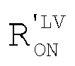
transistors - Since IOFF is a constant value, given by Ip/K, with K constant greater than 1 (chosen as explained hereinafter), we obtain the following formula for the peak value IP:

-
Figure 5a shows the plot of the current IL in time t (µs). The curve of the current IL reaches the peak value IP at the instant tc, when theHV transistor 30a is opened (seeFigure 5b ) and theHV transistor 36a is closed. - Then, between tc and tmax (time interval TCHARGE) the current IL decreases until it reaches the value IOFF=Ip/K.
-
Figure 5b shows, using the same time scale as that ofFigure 5a , the plot of the current ION that flows through theHV transistor 30a during the step ofFigure 4a of charging of theinductor 22b. In the time interval t0-tc the current ION presents the same evolution as the current IL; at the instant tc, theHV transistor 30a is opened and, consequently, the current ION drops to zero.Figure 5c shows, using the same time scale as that ofFigures 5a and 5b , the plot of the output current IOUT. The current IOUT remains at a zero value in the time interval t0-tc, and then reaches the peak value IP at the instant tc, when thecapacitor 27 is electrically coupled to theinductor 22b. Then, between tc and tmax (within the time interval TCHARGE), the energy stored in theinductor 22b supplies and charges thecapacitor 27. - The time interval TCHARGE is given by:

- At time tmax, when the current that flows towards the
capacitor 27 reaches the threshold value IOFF, theHV transistor 36a is opened, and theHV transistor 30a is closed so that theinductor 22b is charged once again, as has already been described. The steps of charging and discharging of theinductor 22b (and, consequently, of supply of thecapacitor 27/load 28) are repeated cyclically. - The integral of the curve of IOUT (
Figure 5c ) between the time tc and the time tmax indicates the charge QCYCLE transferred between the input and the output of therectifier 24 in the time TCHARGE. In order to maximize the efficiency of transfer of charge between the input and the output of therectifier 24, the value of the power PCYCLE transferred at output in each cycle of charge/discharge of theinductor 22b should be maximized. The power PCYCLE is defined as PCYCLE=VOUT·ICYCLE, where ICYCLE is given by ICYCLE= QCYCLE/TCYCLE, where TCYCLE is the time interval elapsing between t0 and tmax (TCYCLE=TDELAY+TCHARGE). - The present applicant has verified that PCYCLE is given by the following relation (where ION assumes the peak value Ip)

- From the foregoing relation it may be noted how the power PCYCLE is a function of the design parameters TDELAY and K, and of the external variables VTRANSD (voltage of the transducer, which is not predictable) and VOUT (voltage on the
capacitor 27, which is not predictable either). Maximizing the value of PCYCLE hence means finding the optimal values of TDELAY and K in such a way that the curve of PCYCLE reaches a maximum value, or a value close to the maximum value, or an optimal value that can be defined according to the particular application and design requirements. - The curve of PCYCLE reaches an optimal value when the output of the
transducer 22 and the input of therectifier circuit 24 show the same impedance (namely, they are matched). The best matching efficiency ηCOUPLE between thetransducer 22 and therectifier circuit 24 is given by PCYCLE OPT/PTRANSD MAX, where PCYCLE OPT is the value of PCYCLE calculated with optimal values of TDELAY and K, and PTRANSD MAX is given by (VTRANSD)2/4Rs. - Optimization of the value of PCYCLE enables an optimal value of the time interval TDELAY and of the factor K to be obtained (and vice versa) as a function of the value of VTRANSD and VOUT. However, the present applicant has verified that the dependence of TDELAY upon VTRANSD and VOUT is irrelevant for practical purposes, and the value of matching efficiency ηCOUPLE reaches values higher than 95% for values of VTRANSD and VOUT of practical interest.
-
Figure 6 shows the evolution of the matching efficiency ηCOUPLE as the values TDELAY and K vary. The graph ofFigure 6 can be obtained easily starting from the expression of PCYCLE by varying the parameters TDELAY and K (fixing the values of the external variables VTRANSD and VOUT). Corresponding to each value of ηCOUPLE is a pair of values TDELAY and K. It is thus possible to derive in an automatic way the pair of optimal values TDELAY and K to obtain a desired value of matching efficiency ηCOUPLE. In the graph ofFigure 6 , the darker areas are those in which the value of matching efficiency ηCOUPLE is higher; instead, the lighter areas are those in which the value of matching efficiency ηCOUPLE is lower (low values of TDELAY and high values of K, or high values of TDELAY and low values of K). -
Figure 7 shows profiles of current IL in theinductor 22b as pairs of values of TDELAY and K vary, and with reference to a optimal ideal current value IL OPT (condition of matched load in which the matching efficiency is maximum). - In particular, the
curve 65 shows the cyclic pattern, in time t, of the profiles of current IL for high values of TDELAY and K (for example, TDELAY=100µs and K=5). In this case, there is the advantage that the frequency of opening/closing of theHV transistors HV transistors rectifier circuit 24 during use. However, the values of peak current Ip reached by the current IL according to thecurve 65 are high, and the impedance matching between thetransducer 22 and therectifier circuit 24 other than optimal, causing a relatively low matching efficiency ηCOUPLE (ηCOUPLE≈72.3%). - The
curve 67 shows the cyclic pattern, in time t, of the profiles of current IL for average values of TDELAY and K (for example, TDELAY=30µs and K=2.25). In this case, the frequency of opening/closing of theHV transistors HV transistors curve 65, but there is the advantage that the values of peak current are lower than in the case of thecurve 65 and the matching efficiency is high (ηCOUPLE≈96.5%). - Finally, the
curve 69 shows the cyclic pattern, in time t, of the profiles of current IL for peak values of TDELAY and K (for example, TDELAY=10µs and K=1.3). In this case, the matching efficiency ηCOUPLE is still higher than in the case of the curve 67 (approximately 99.5%), but with the disadvantage that the driving frequency of theHV transistors HV transistors rectifier circuit 24, with consequent reduction in the efficiency factor ηSCAV not sufficiently compensated for by the increase in the value of matching efficiency ηCOUPLE. - For the purposes of application of the
rectifier circuit 24 as energy-scavenging interface in an environmental-energy-scavenging system, a compromise choice, such as for example that of thecurve 67, is preferable. It is evident that other contexts of application of the present invention may lead to a different choice of the values of TDELAY and K (and, in general, with K≥1). -
Figure 8 shows, by means of functional blocks, acontrol circuit 70 for driving theHV transistor 30a and theHV transistor 36a in order to implement the operating conditions ofFigures 4a and 4b . Thecontrol circuit 70 operates, in particular, for positive half-waves (VIN +) of the input signal VIN. TheLV transistor 36b is biased with a gate-to-source voltage (VGS) equal to VDD, whereas theLV transistor 30b is biased at a constant voltage VDD, in such a way as to be kept always in the on state. The value of the voltage VDD is hence chosen on the basis of the characteristics of thetransistors - In order to operate the
HV transistor 31a and theHV transistor 38a for negative half-waves of the input signal VIN, a circuit architecture similar to the one shown for thecontrol circuit 70 is used (not shown in detail inFigure 8 ). - In greater detail, the
control circuit 70 comprises a firstcurrent detector 72, coupled between the source terminal S and the drain terminal D of theLV transistor 30b, for detecting (during the step ofFigure 4a ) when the current ION that flows through theLV transistor 30b (and, consequently, also through theHV transistor 30a) exceeds the threshold ITH. Moreover, thecurrent detector 72 has also the function of generating, in the step ofFigure 4a , a scaled copy of the current that flows in theLV transistor 30b, as illustrated more fully in what follows. -
Figure 9 shows in greater detail the firstcurrent detector 72, according to an embodiment. With reference to saidFigure 9 , a first portion of thecurrent detector 72 comprises acomparator 86 configured for receiving at input the voltage signals present on the source terminal S and on the drain terminal D of theLV transistor 30b and generating at output a digital signal that assumes a low logic level when ION<ITH and a high logic level when ION≥ITH (or vice versa). The signal at output from thecomparator 86 is supplied to thecontrol logic 60, which, once the time interval TDELAY has elapsed, opens theHV transistor 30a. - The duration of the time interval TDELAY, according to the amplitude of the signal VTRANSD of the
transducer 22a, can be determined either by thecontrol logic 60 or by thecomparator 86 belonging to thecurrent detector 72. - In the latter case, the signal at output from the
comparator 86 assumes a high logic level when ION≥ITH and t≥TDELAY, and thecontrol logic 60 opens theHV transistor 30a at the rising edge of the digital signal generated by thecomparator 86. - A second portion of the
current detector 72 comprises a negative-feedback loop including anamplifier 89 that controls the current that flows on anoutput branch 90 of thecurrent detector 72 by acting on the control terminal of atransistor 91 belonging to the output branch 90 (i.e., by opening/closing the transistor 91). The negative feedback ensures that the voltage on the inverting input of theamplifier 89 is always equal to the voltage present on the non-inverting input of theamplifier 89. Theoutput branch 90 moreover comprises afurther transistor 92 having dimensions (understood as W/L ratio) that are smaller by a factor F than the respective dimensions (understood as W/L ratio) of theLV transistor 36b. - In use, current always flows in the
output branch 90. In the step ofFigure 4a the current is variable and equal to ION/F, while in the step ofFigure 4b the current is constant and equal to IP/F. Sizing of thetransistor 92 guarantees that the current that flows in theoutput branch 90 is afraction 1/F of the current ION (or of its peak value IP, as has been said). - To return to
Figure 8 , thecontrol circuit 70 further comprises a secondcurrent detector 74, coupled to the source terminal S and to the drain terminal D of theLV transistor 36b. The secondcurrent detector 74 is similar to the firstcurrent detector 72 and is configured for detecting the value of current that flows through theLV transistor 36b (and, consequently, through theHV transistor 36a) during the operating step ofFigure 4b . In particular, the secondcurrent detector 74 co-operates with thecontrol logic 60 in order to detect whether the current IOUT reaches the minimum expected value IOFF=IP/K. The output signal of the secondcurrent detector 74, indicating the current value IOUT, is supplied at input to thecontrol logic 60. - The second
current detector 74 receives at input the current ION/F (generated by the firstcurrent detector 72, as has been described previously), and switches when the current IOUT reaches the minimum expected value given by IOFF=IP/K. - The
control circuit 70 further comprises afirst driving device 76 and asecond driving device 78, coupled, respectively, between thecontrol logic 60 and the control terminal G of theHV transistor 30a and of theHV transistor 36a. Thefirst driving device 76 and thesecond driving device 78 are, in themselves, of a known type, and are designed to drive into an open/closed state thetransistors control logic 60. In particular, in the operating condition ofFigure 4a , thecontrol logic 60 drives, via thefirst driving device 76, theHV transistor 30a into the closed state and, via thesecond driving device 78, theHV transistor 36a into an open state. - When, on the basis of the signal generated at output from the first
current detector 72, thecontrol logic 60 detects that the current IL=ION has reached (and/or exceeded) the threshold value ITH, and the time TDELAY has elapsed, thecontrol logic 60 drives, via thefirst driving device 76, theHV transistor 30a into an open state and, via thesecond driving device 78, theHV transistor 36a into the closed state. Then, thecontrol logic 60 monitors, on the basis of the signal received from the secondcurrent detector 74, the value of the current IOUT for controlling passage from the current operating condition (of supply of the load,Figure 4b ) to the operating condition of storage of energy in theinductor 22b (Figure 4a ), as soon as the current IOUT reaches the value IOFF. - The
control circuit 70 further comprises afirst voltage detector 80 and asecond voltage detector 82, which are, respectively, coupled between the control terminal G and the source S of theHV transistor 30a and of theHV transistor 36a. Thefirst voltage detector 80 detects the voltage present between the control terminal G of theHV transistor 30a and the source terminal S of theLV transistor 30b (in this case, corresponding to the reference terminal GND) and generates an output signal indicating said voltage. The output signal generated by thefirst voltage detector 80 is supplied to thecontrol logic 60. Likewise, thesecond voltage detector 82 detects the voltage present between the control terminal G of theHV transistor 36a and the source terminal S of theLV transistor 36b (in this case, corresponding to the input node 25') and generates an output signal indicating said voltage. On the basis of the signals received by the first andsecond voltage detectors control logic 60 knows the state, whether on or off, of theHV transistors Figure 4a to the operating condition ofFigure 4b (and vice versa) inserting appropriate dead times between opening (closing) of theHV transistor 30a and closing (opening) of theHV transistor 36a. There are thus prevented phenomena of cross conduction and direct connection between the first output terminal 26' (to which thecapacitor 27/load 28 is coupled) and the ground-reference terminal GND. - What has been described herein, both from a circuit standpoint and from the standpoint of method for operating the
control circuit 70, can be applied in a corresponding way evident for the person skilled in the sector, to theHV transistors LV transistors LV transistors -
Figure 9 shows, according to an embodiment of the present invention, the firstcurrent detector 72. According to the embodiment ofFigure 9 , the firstcurrent detector 72 further comprises means designed to store the peak value Ip of the current ION that traverses, in use, theHV transistor 30a.Figure 9 shows moreover, coupled to the firstcurrent detector 72, acomparator 86 the output signal of which indicates, for thecontrol logic 60, whether the current IL=ION reaches (or exceeds) the threshold value ITH set. - The
comparator 86 is configured for receiving, at input to the non-inverting terminal, the voltage signal present on the input terminal 25' of the rectifier circuit 24 (signal VIN +), and, at input to the inverting terminal, a threshold-voltage signal VTH in such a way that VTH=ITH·(RHV ON+RLV ON), where, as has already been said, RHV ON is the on-state resistance of theHV transistor 30a and RLV ON is the on-state resistance of theLV transistor 30b. When the voltage on the input terminal 25' exceeds the threshold VTH, the output of thecomparator 86 changes state, signalling the fact that the threshold has been exceeded (and hence indicating that IL=ION≥ITH). - The first
current detector 72 further comprises atransistor 87 having a drain terminal common to the drain terminal of theLV transistor 30b, and its source terminal coupled to a capacitor 88 (the second terminal of thecapacitor 88 is connected to the reference voltage GND). The control terminal G of thetransistor 87 is connected to the control terminal G of theHV transistor 30a. In this way, theHV transistor 30a and thetransistor 87 are driven into an open/closed state by one and the same signal VGATE_LS. - During the time interval TDELAY (situation of
Figure 4a ), theHV transistor 30a is closed (the signal VGATE_LS has a high value and drives theHV transistor 30a into the closed state). Likewise, also thetransistor 87, is closed. Thecapacitor 88 is consequently charged to the voltage present on the first input terminal 25' of the rectifier circuit 24 (inFigure 9 the voltage across thecapacitor 88 is designated by VC_SAMPLE). - The first
current detector 72 moreover comprises afurther comparator 89 and abranch 90 including atransistor 91 and atransistor 92 connected in series together between a terminal 90' and the reference terminal GND. In particular, thetransistor 91 has its own source terminal coupled to the drain terminal of thetransistor 92; moreover, thetransistor 92 has its own control terminal G connected to a constant-voltage supply terminal VDD. It should be noted that thetransistor 92 is a low-voltage transistor, for example a CMOS. In particular, thetransistor 92 is able to operate with gate-to-source voltages in the 1-5 V range, in particular 2.5V-3.6 V, for example 3.3 V. Other technologies for low-voltage transistors envisage slightly higher operating voltages, for example in the region of 4-5 V. In particular, thetransistor 92 is of the same type as theLV transistor 30b, but is sized so thetransistor 92 has dimensions (measured in terms of shape factor W/L, width/length) F times smaller than theLV transistor 30b and is designed to conduct a current F times lower than the value assumed by ION (current that flows through theLV transistor 30b). TheLV transistor 30b and thetransistor 92 moreover have their respective control terminals connected together and biased at the voltage VDD. The negative feedback, provided by means of thecomparator 89 and thetransistor 91, ensures that the drain voltages of thetransistors transistor 92 assumes values equal to the value of ION scaled by the factor F (when ION reaches the peak value Ip said current will be equal to Ip/F). There is thus generated a scaled copy of the factor F of the peak current IP. Since both of thetransistors transistors 30b and 92 (as, instead, the case if thetransistor - The
comparator 89 is connected to the source terminal of thetransistor 87, and, when thetransistor 87 is closed, it receives at input (on the non-inverting terminal) the voltage of the drain terminal of theLV transistor 30b, and at input (on the inverting terminal) the signal present on the drain terminal of thetransistor 92 and source terminal of thetransistor 91; the output of thecomparator 89 is coupled to the control terminal G of thetransistor 91. Thetransistor 91 is always closed; thecomparator 89 biases the control terminal of thetransistor 91 in such a way that on thebranch 90 there flows the current ION/F, as desired. - The negative feedback provided by the
comparator 89 ensures that the signal at input to the non-inverting terminal of thecomparator 89 and the signal at input to the inverting terminal of thecomparator 89 are equal, so that theLV transistor 30b and thetransistor 92 will have the same source-to-drain and source-to-gate voltages. - When the
HV transistor 30a is open, also thetransistor 87 is open, and thecapacitor 88 is in a floating state, ensuring, during the time interval TCHARGE, a current of a practically constant value, and equal to the value IP/F, through thetransistor 92. - In fact, during the step of supply of the
capacitor 27/load 28, thecapacitor 88 ensures maintenance of the voltage VC_SAMPLE across it, guaranteeing an input signal that is substantially constant (but for the losses of the capacitor 88) on the non-inverting input of thecomparator 89. This makes it possible to keep unaltered the generation of the current ION/F on theoutput branch 90 of the firstcurrent detector 72 during the step ofFigure 4b (in this step, the current ION has reached the peak value IP, and consequently flowing in theoutput branch 90 of the firstcurrent detector 72 is a current IP/F). -
Figure 10a shows graphically the time plot of the voltage on the drain terminal of theLV transistor 30b and of the voltage signal VC_SAMPLE across thecapacitor 88. These signals have the same evolution and coincide with one another inFigure 10a. Figure 10b shows the time plot of the signal VGATE_LS applied to the control terminals of theHV transistor 30a and of thetransistor 87. - At the end of TCHARGE the voltage VC_SAMPLE drops to the value IOFF · (RHV ON+RLV ON) where RHV ON and RLV ON are, respectively, the on-state resistances of the
HV transistor 30a and theLV transistor 30b. -
Figure 11 shows, in greater detail, the secondcurrent detector 74. The secondcurrent detector 74 ofFigure 11 comprises atransistor 97, having a source terminal S connected to the first input terminal 25' of therectifier circuit 24, a control terminal G connected to the control terminal G of theLV transistor 36b, and a drain terminal D. In parallel to the transistor 97 aresistor 98 is shown representing the on-state electrical resistance RON_DMY of thetransistor 97. Likewise, also theLV transistor 36b and theHV transistor 36a are shown with their own respective on-state electrical resistances

resistors 96 and 95). - The second
current detector 74 further comprises acomparator 99, having an inverting terminal connected between the drain terminal of theLV transistor 36b and the source terminal of theHV transistor 36a (to receive an intermediate output signal VOUT_INT), and a non-inverting terminal connected to the drain terminal of the transistor 97 (to receive an intermediate reference signal VREF_INT). - The
transistor 97 is a replica, scaled by a factor J, of theLV transistor 36b. Consequently, thetransistors transistor 97 has dimensions (measured in terms of shape factor W/L, width/length) that are J times smaller than those of theLV transistor 36b and is designed to conduct a current F times lower than the value assumed by ION (i.e., ION/F) during the step ofFigure 4a , and a current F times lower than the peak value IP (i.e., IP/F) during the step ofFigure 4b . - The intermediate voltage signal VREF_INT at input to the comparator 99 (on the non-inverting terminal) is given (at time tc of
Figure 5c ) by:
- The voltage signal VOUT_INT at input to the comparator 99 (on the inverting terminal) is given by:

transistors - It follows that, since the condition that determines the change of the output of the
comparator 99 is VREF_INT=VOUT_INT, the value of IOUT at which there is a change of output of thecomparator 99 is precisely the current value IOFF previously introduced. Consequently, since IOUT=IOFF, we obtain IOFF=J/F·Ip, and, defining K=F/J, the condition previously indicated (IOFF=Ip/K) that determines the threshold of passage from the operating condition ofFigure 4b to the operating condition ofFigure 4a is obtained. - It is pointed out that both of the
transistors transistors 36b and 97 (as, instead, would be the case if both of the transistors were high-voltage transistors). Stabilizing J around a value corresponds desired to stabilizing the value of K around the value chosen. Moreover, since also the factor F is stable, the parameter K has a minimal spread around the chosen and desired value. -
Figures 12a-12c show, using one and the same time scale: the plot of the signals VIN +, VREF_INT, VOUT (Figure 12a ); the plot of the signal VOUT_COMP generated at output from the comparator 99 (Figure 12b ); and the plot of the current signal IL (Figure 12c ). - With reference to
Figure 12a , it may be noted that to an (ideal) rising edge of the input signal VIN + there corresponds a progressive fall of the signal VREF_INT and a corresponding progressive rise of the signal VOUT. Hence, with further reference toFigure 12b , when VREF_INT=VOUT (instant tx), the output VOUT_COMP of thecomparator 99 changes state and passes from a low-value state a high-value state. The change of state is recognized by thecontrol logic 60, which controls accordingly the HV switches (transistors) 30a and 36a as has been described previously. -
Figure 12c shows the current IL, in particular during the time interval TCHARGE (operating condition ofFigure 4b ). The current IL=IOUT decreases from a maximum value IP to a value minimum IOFF, supplying thecapacitor 27/load 28. - What has been described previously applies, in an altogether equivalent way, to control of the HV switches (transistors) 31a and 38a, for negative polarities of the input voltage VIN.
- The
control logic 60 implements the method of control of theHV transistors Figure 13 , by means of a flowchart. - With reference to
Figure 13 ,step 100, theHV transistors HV transistors 36a and 38, instead, are opened. In the sequel of the description theLV transistors Figure 3b ). - In this way, the
inductor 22b is charged via the current IL=ION that flows through theHV transistors - The current value IL=ION is monitored (step 102) for detecting whether it reaches (or exceeds) the required threshold value ITH. At the same time, the
control logic 60 monitors the time interval TDELAY. In this case, the time to of start of the time interval TDELAY corresponds to the closing instant of theHV transistors step 100. - In the case where the current IL has not reached the threshold ITH or the time TDELAY has not elapsed (output NO from step 102), it is necessary to wait for both of these conditions to be met, and the
control logic 60 keeps thesystem 20 in thestates next step 104. - During step 104 a check is made to verify whether the input voltage VIN has a positive polarity or a negative polarity. This operation can be carried out by means of the
comparator 86, which receives at input the signal VIN +. - As has already been said, a circuit equivalent to the shown in
Figure 9 is coupled (in a way not shown in Figure) to theHV transistor 31a, and used in a similar way to verify whether the input voltage VIN has a negative polarity. - In the case where the input voltage VIN has a positive polarity, control passes to step 106 (output YES from step 104), where the
HV transistor 30a, and possibly theLV transistor 30b, are opened to supply thecapacitor 27/load 28 via theHV transistors 36a andLV switch 36b. - In the case where the input voltage VIN has negative polarity, control passes, instead, to step 108 (output NO from the step 104), where the
capacitor 27/load 28 is supplied via theLV transistor 38b andHV transistor 38a. - Exit from
steps control logic 60 monitors the value of current IOUT that flows through theLV transistor 36b (or theLV transistor 38b according to the polarity of the input voltage VIN) towards the output of therectifier 24 for detecting whether the current IOUT assumes a value equal to IOFF. As long as IOUT>IOFF, thecontrol logic 60 keeps thesystem 20 in the step of charging of thecapacitor 27/supply of theload 28. When IOUT=IOFF, control returns to step 100. The steps 100-104 are executed, as described with reference toFigures 5a-5c , in a time interval equal to at least TDELAY until the current in the inductor reaches the threshold ITH whereas the steps 106-110 are executed within the time interval TCHARGE. - The
control logic 60 is, for example, a microcontroller configured for driving theHV transistors Figure 13 . -
Figure 14 shows avehicle 200 comprising the energy-scavengingsystem 20 ofFigure 3 . Thevehicle 200 is, in particular, a motor vehicle. It is evident, however, that the energy-scavengingsystem 20 can be used in anyvehicle 200 or in systems or apparatuses different from a vehicle. In particular, the energy-scavengingsystem 20 can find application in generic systems in which it is desirable to harvest, store, and use environmental energy, in particular by means of conversion of mechanical energy into electrical energy. - With reference to
Figure 14 , thevehicle 200 comprises one ormore transducers 22 coupled in a known way to a portion of thevehicle 200 that is subject to mechanical stresses and/or vibrations, for converting said mechanical stresses and/or vibrations into electric current. - The energy-scavenging
system 20 is connected to one or more electrical loads 28a, ..., 28n, for example via interposition of a DC-DC converter. In particular, according to an application of the present invention, the electrical loads 28a, ..., 28n comprise TPM (tyre-parameter monitoring)sensors 250 for monitoring parameters oftyres 202. In this case, theTPM sensors 250 are coupled to an internal portion of thetyres 202 of thevehicle 200. Likewise, also the transducers 22 (for example, of an electromagnetic or piezoelectric type) are coupled to an internal portion of thetyres 202. The stress of thetransducers 22 when thevehicle 200 is travelling causes production of an electric current/voltage signal at output from thetransducer 22 by means of conversion of the mechanical energy into electrical energy. The electrical energy thus produced is stored, as has been described previously, in thestorage element 27 and supplied, via the DC-DC converter that may possibly be present, to theTPM sensors 250. - According to one embodiment of the present invention, the energy-scavenging
system 20, comprising one or more transducers, and theTPM sensors 250, are glued inside one ormore tyres 202. Impact of thetyres 202 on the ground during motion of thevehicle 200 enables production of electrical energy. - As an alternative to what is shown in
Figure 14 , the energy-scavengingsystem 20 can be arranged in any other portion of thevehicle 200, and/or used for supplying an electrical load other than or additional to theTPM sensors 250. - Another possible application of the energy-scavenging
system 20 is the generation of electrical energy by exploiting the mechanical energy produced by a person when he is walking or running. In this case, the energy-scavengingsystem 20 is set inside theshoes 300 of said person (for example, inside the sole) as shown schematically inFigure 15 . In systems aimed at fitness, where it is of particular interest to count the steps, it is useful to recover energy from the vibrations induced by walking/running in order to be able to supply without using batteries acceleration sensors and/or RFID transmitters that are able to communicate with cellphones, music-player devices, or any other apparatus that might require information on the steps made. - From an examination of the characteristics of the invention provided according to the present disclosure the advantages that it affords are evident.
- In particular, the parameter K has a highly riproducible value (minimum spread) so as to increase the performance, robustness and efficiency of the
system 20, minimizing the mismatch between the positive and negative polarities of the signal of the transducer and preventing phenomena of reversal of the flow of current from thecapacitor 27 to theinput terminals 25', 25" of therectifier circuit 24. - Moreover, since the duration of the time interval TDELAY is (typically) constant, the
rectifier 24 operates at constant duty cycle of the signal of opening/closing of the first andsecond switches 30, 31. This enables values of efficiency ηSCAV (efficiency of therectifier 24, having the function of scavenging interface of the system 20) to be obtained that are particularly high (the present applicant has found efficiency values higher than 95% irrespective of the values assumed by VTRANSD and VOUT). - The scavenging efficiency is moreover high even when the amplitude of the signal VTRANSD of the
transducer 22 is lower than the voltage value stored in thecapacitor 27, overcoming a limitation of the diode-bridge rectifier architecture. - Moreover, since in the case of a
transducer 22 of an electromagnetic type therectifier 24 exploits theinductor 22b inside thetransducer 22, the scavenging efficiency is high even when the amplitude of the signal of the transducer is low. - The limitation imposed by diode-bridge rectifiers, which require a voltage of the transducer VTRANSD higher than 2VTH_D, where VTH_D is the threshold voltage of the diodes of the rectifier, is in this way overcome.
- Using an HV (high-voltage) technology for the
capacitor 27 and for the scavenging interface, it is possible to store high voltages, and hence a high energy, in the capacitor, increasing the autonomy of operation of theTPM sensors 250 accordingly. - The method described, which envisages the choice of an optimal value of TDELAY and of K, enables implementation of an active control (of the mean value and of the ripple) of the current supplied by the transducer, and enables an optimal matching of impedance between the
transducer 22 and the scavenginginterface 24. This ensures an efficiency ηSCAV of the scavenging interface 24b that is high irrespective of the velocity of rotation of thetyres 202 and of the conditions of storage of energy in thecapacitor 27. - Moreover, as has been said, the value of the interval TDELAY may be varied according to the particular application in which the
rectifier 24 operates. Therectifier 24 thus finds use in systems other than the energy-scavengingsystem 20, i.e., ones based upon electromagnetic transducers of any type. - In addition, the
rectifier circuit 24 may be used with transducers of another type, by interposition of an appropriate circuit between the transducer and the rectifier circuit designed to provide a storage of energy similar to theinductor 22b. - Moreover, the
rectifier 24 according to the present invention and the energy-scavengingsystem 20 are of a fully integrated type, and consequently require minimal space for installation. - Finally, harvesting of environmental energy is obtained even when the signal of the transducer is lower than the voltage value stored on the output capacitor, something which is not possible using an diode-bridge interface of a known type as shown in
Figure 1 . According to the present invention, the scavenginginterface 24 is hence able to harvest energy even when the power supplied by the transducer is very low. - Finally, it is clear that modifications and variations may be made to what has been described and illustrated herein, without thereby departing from the sphere of protection of the present invention, as defined in the annexed claims.
- In particular, according to an embodiment of the present invention, the
rectifier circuit 24 may comprise a number of transistors different from the one described. For example, therectifier circuit 24 may be a half-wave rectifier, comprising only the switches that operate for positive polarity of the input signal VIN (i.e., theswitches switches - The use of a half-wave rectifier may be advantageous in the case where the input signal VIN is of a known type and comprises only positive (or negative) half-waves. Its use is, however, not recommended (even though it is possible) in energy-scavenging systems in so far as part of the input signal would be lost, at the expense of the efficiency of the system as a whole.
- In addition, the conditions t>TDELAY and IL>ITH expressed with reference to the operating condition of
Figure 4a are not always both necessary. In particular, for voltage signals generated bytransducers 22 of a known type the voltage value always reaches peaks such as to enable the threshold ITH to be exceeded within the time TDELAY. Moreover, an appropriate choice of TDELAY always guarantees, for practical purposes, that an acceptable minimum threshold ITH is reached. - Furthermore, there may be present a plurality of
transducers 22, all of the same type or of types different from one another, indifferently. For example, the transducer/transducers may be chosen in the group comprising: electrochemical transducers (designed to convert chemical energy into an electrical signal), electromechanical transducers (designed to convert mechanical energy into an electrical signal), electroacoustic transducers (designed to convert pressure variations into an electrical signal), electromagnetic transducers (designed to convert a magnetic field into an electrical signal), photoelectric transducers (designed to convert light energy into an electrical signal), electrostatic transducers, thermoelectric transducers, piezoelectric transducers, thermoacoustic transducers, thermomagnetic transducers, thermoionic transducers.
Claims (20)
- An energy-scavenging interface (24) having a first input terminal (25') and a second input terminal (25") connectable to respective terminals of a first storage element (22b), and a first output terminal (26') and a second output terminal (26") connectable to respective terminals of a second storage element (27), wherein the first and second input terminals (25', 25") are configured to receive an electrical input signal (VIN), and the first and second output terminals are configured to supply to the second storage element an output signal (IOUT, VOUT), the energy-scavenging interface (24) comprising: a first switch (30a, 31a) and a second switch (30b, 31b) connected in series to one another, between the first input terminal (25'; 25") and the second output terminal (26"); a third switch (36a, 38a) and a fourth switch (36b, 38b), connected in series to one another, between the first input terminal (25'; 25") and the first output terminal (26'); a first electrical-signal detecting device (72), coupled to conduction terminals of the second switch (30b; 31b) configured for detecting whether the electric current in the storage element (22b) reaches a threshold value (ITH); and a control logic (60, 70) configured for:- controlling the first and second switches (30a, 30b; 31a, 31b) in a on-state and the third switch (36a; 38a) in an off-state for a first time interval having at least one first time duration (TDELAY) during which the first storage element (22b) stores electric charge and until the electrical charge stored by the storage element (22b) reaches the threshold value (ITH);- acquiring, once the first time interval (TDELAY) has elapsed and once the threshold value (ITH) has been reached, a scaled copy (Ip/K) of a peak value (Ip) of the electric current stored in the storage element (22b);- controlling the first switch (30a; 31a) in an off-state and the third and fourth switches (36a, 36b; 38a, 38b) in a on-state to generate the output signal that supplies the second storage element;- maintaining the first switch (30a; 31a) in the off-state and the third and fourth switches (36a, 36b; 38a, 38b) in the on-state as long as the current value of the output signal (IOUT) is higher than the value of said scaled copy (Ip/K) of the peak value.
- The energy-scavenging interface according to claim 1, further comprising:- a sampling capacitor (88) electrically coupled between a conduction terminal of the second transistor (30b; 31b) and the second output terminal (26", GND) for acquiring and storing an electrical signal (VC_SAMPLE) indicating said peak value (Ip); and- a first current-scaling switch (92), maintained in the on-state together with the second switch (30b; 31b) and configured for carrying an electric current having a value that reduced, with respect to the peak value (Ip), by a first scaling factor F.
- The energy-scavenging interface according to claim 1 or claim 2, wherein the first and third switches (30a, 36a; 38a, 38b) are high-voltage transistors, and the second and fourth switches are low-voltage transistors.
- The energy-scavenging interface according to claim 3 when depending on claim 2, wherein the first current-scaling switch (92) is a low-voltage transistor having a width/length (W/L) shape factor that is reduced, with respect to the W/L shape factor of the second switch (30b; 31b), by a value equal to said first scaling factor F.
- The energy-scavenging interface according to any one of the preceding claims, wherein said scaled copy (Ip/K) corresponds to the peak value (Ip) reduced by a scale factor (K), the first time duration (TDELAY) and the scale factor (K) being chosen of a value such as to optimize the matching efficiency to the input port of the energy-scavenging interface (24).
- The energy-scavenging interface according to claim 2 or any one of claims 3-5 when depending upon claim 2, further comprising a second electrical-signal detecting device (74) coupled to the conduction terminals of the fourth switch (36b; 38b) and configured for:- acquiring a value in current of the output signal (IOUT) that flows through the fourth switch (36b); and- detecting when the value in current of the output signal (IOUT) assumes a value equal to said scaled copy (Ip/K) of the peak value (Ip), the second electrical-signal detecting device (74) further including:- a second current-scaling switch (97) kept in the on-state together with the fourth switch (36b; 38b) and configured for carrying an electric current having a value that is reduced, with respect to the value in current of the output signal (IOUT), by a second scaling factor J; and- a comparator (99) configured for receiving at input a signal indicating the output signal (VOUT_INT) and a signal indicating the electric current carried by the second current-scaling switch (97), and for supplying at output a comparison signal (VOUT_COMP) indicating a result of the comparison between the signals at input to the comparator (99), the second current-scaling switch (97) being traversed, during the second time interval, by an electric current having a value equal to the peak value (Ip) reduced by the first scaling factor F, said comparison signal (VOUT_COMP) having a logic value identifying the fact that the output signal (IOUT) assumes a value reduced by a scale factor K, where K is given by the ratio between the first scaling factor F and the second scaling factor J.
- The energy-scavenging interface according to claim 6, wherein the second current-scaling switch (97) is a low-voltage transistor having width/length (W/L) shape factor that is reduced, with respect to the shape factor of the fourth switch (36b; 38b), by a value equal to said second scaling factor J.
- The energy-scavenging interface according to any one of the preceding claims, wherein the input port can be coupled to a transducer (22) of an electromagnetic type including an inductor (22b), said storage element (22b) being the inductor of said transducer (22) of an electromagnetic type.
- The energy-scavenging interface according to claim 5 or claim 6, wherein the control logic (60) is moreover configured for:- defining said matching efficiency as a function of the first time duration (TDELAY) and of the scale factor (K);- acquiring a plurality of values of matching efficiency associated to a respective plurality of values of said first time duration (TDELAY) and to a respective plurality of values of the scale factor (K); and- identifying a value of said first time duration (TDELAY) and a value of the scale factor (K) such as to optimize the matching efficiency at the input port of the energy-scavenging interface (24).
- The energy-scavenging interface according to any one of the preceding claims, wherein said first time duration (TDELAY) is comprised between approximately 1 µs and 100 µs.
- The energy-scavenging interface according to any one of the preceding claims, wherein the scale factor (K) is chosen of a value greater than 1.
- An energy-scavenging system (20) configured to supply an electrical load (28), comprising:- a transducer (22), configured for converting energy coming from an energy source external to said system (20) into a transduced electrical signal (VTRANSD, VIN);- an electrical-energy-scavenging interface (24) according to any one of claims 1-11, configured for receiving at input the transduced electrical signal and for supplying at output an output signal (VOUT); and- a first storage element (27) coupled to the electrical-energy-scavenging interface (24) to receive at input the output signal (VOUT), and configured for storing electrical energy designed to supply the electrical load (28).
- The system according to claim 12, further comprising a DC-DC converter (6) connected between a first storage element (27) and the electrical load (28), said DC-DC converter (6) being configured for supplying the electrical load (28) via the electrical energy stored in the first storage element (27).
- The apparatus (100) comprising the energy-scavenging system (20) according to claim 12 or claim 13.
- The apparatus according to claim 14, chosen between a vehicle and an item of sports footwear.
- A method for scavenging energy by means of an energy-scavenging interface (24) having an input port (25', 25") connectable to a first storage element (22b), and an output port (26', 26") connectable to a second storage element (27), wherein the input port is configured to receive an electrical input signal (VIN), and the output port is configured to supply to the electrical load an output signal (IOUT, VOUT),
the method comprising the steps of:- receiving, at the input port, an electrical input signal (VIN, IL);- charging, by means of the electrical input signal (VIN, IL), the first storage element (22b) for at least a first time interval having a time duration (TDELAY) and until the electrical charge stored by the storage element (22b) reaches a threshold value (ITH);- acquiring a scaled copy (Ip/K) of the peak value (Ip) of the electric current stored in the storage element (22b); and- supplying the second storage element (27) by means of the electric current stored in the first storage element (22b) as long as the value in current of the output signal (IOUT) is higher than the value of said scaled copy (Ip/K) of the peak value (Ip). - The energy-harvesting method according to claim 16, further comprising the steps of:- acquiring the peak value (Ip) of the associated electric current stored in the storage element (22b);- scaling by a scale factor (K) said peak value (Ip) of the electric current to obtain said scaled copy (Ip/K); and- identifying the time duration (TDELAY) and the scale factor (K) in such a way that the matching efficiency (ηCOUPLE) between the transducer (22) and the energy-scavenging interface (24) is optimal.
- The energy-harvesting method according to claim 17, wherein the identification step comprises:- defining said matching efficiency as a function of the time duration (TDELAY) and of the scale factor (K); and- acquiring a plurality of values of matching efficiency associated to a respective plurality of values of said time duration (TDELAY) and to a respective plurality of values of the scale factor (K).
- The energy-harvesting method according to any one of claims 16-18, further comprising the step of choosing said first time duration (TDELAY) of constant value, for example comprised between approximately 1 µs and 100 µs.
- The energy-harvesting method according to any one of claims 16-19, further comprising the step of choosing the first scale factor (K) of a value greater than 1.
Applications Claiming Priority (1)
| Application Number | Priority Date | Filing Date | Title |
|---|---|---|---|
| IT000847A ITTO20120847A1 (en) | 2012-09-27 | 2012-09-27 | ENERGY COLLECTION INTERFACE WITH IMPROVED EFFICIENCY, METHOD TO OPERATE THE ENERGY COLLECTION INTERFACE, AND ENERGY COLLECTION SYSTEM INCLUDING THE ENERGY COLLECTION INTERFACE |
Publications (3)
| Publication Number | Publication Date |
|---|---|
| EP2713500A2 true EP2713500A2 (en) | 2014-04-02 |
| EP2713500A3 EP2713500A3 (en) | 2018-03-21 |
| EP2713500B1 EP2713500B1 (en) | 2020-01-22 |
Family
ID=47226347
Family Applications (1)
| Application Number | Title | Priority Date | Filing Date |
|---|---|---|---|
| EP13186555.2A Active EP2713500B1 (en) | 2012-09-27 | 2013-09-27 | Enhanced-efficiency energy-scavenging interface, method for operation and energy-scavenging system comprising the interface |
Country Status (3)
| Country | Link |
|---|---|
| US (2) | US9461504B2 (en) |
| EP (1) | EP2713500B1 (en) |
| IT (1) | ITTO20120847A1 (en) |
Cited By (2)
| Publication number | Priority date | Publication date | Assignee | Title |
|---|---|---|---|---|
| CN105429454A (en) * | 2014-09-17 | 2016-03-23 | 意法半导体股份有限公司 | Efficient Energy Harvesting Interface and Corresponding Energy Harvesting System |
| US10211722B2 (en) | 2015-04-29 | 2019-02-19 | Stmicroelectronics S.R.L. | Energy scavenging interface with impedance matching, method for impedance matching of the energy scavenging interface, and energy scavenging system using the energy scavenging interface |
Families Citing this family (6)
| Publication number | Priority date | Publication date | Assignee | Title |
|---|---|---|---|---|
| US8630148B2 (en) * | 2011-06-02 | 2014-01-14 | Schlumberger Technology Corporation | Systems, methods, and apparatus to drive reactive loads |
| DE102013107721A1 (en) * | 2013-07-19 | 2015-01-22 | Sma Solar Technology Ag | Inverter with at least two DC inputs, photovoltaic system with such an inverter and method for controlling an inverter |
| JP6670937B2 (en) * | 2015-12-03 | 2020-03-25 | コーニンクレッカ フィリップス エヌ ヴェKoninklijke Philips N.V. | Energy generation system and method |
| US10243136B2 (en) * | 2016-08-22 | 2019-03-26 | Masoud Ghanbari | Piezoelectric energy harvesting system from vehicle's tires |
| FR3069395A1 (en) * | 2017-07-18 | 2019-01-25 | Commissariat A L'energie Atomique Et Aux Energies Alternatives | PIEZOELECTRIC GENERATOR |
| US11482949B2 (en) * | 2018-12-03 | 2022-10-25 | Honeywell Federal Manufacturings Technologies, Llc | Electrostatic harvester device |
Family Cites Families (39)
| Publication number | Priority date | Publication date | Assignee | Title |
|---|---|---|---|---|
| JPS62210834A (en) | 1986-03-10 | 1987-09-16 | セイコーインスツルメンツ株式会社 | Capacitor charging circuit |
| US5617015A (en) | 1995-06-07 | 1997-04-01 | Linear Technology Corporation | Multiple output regulator with time sequencing |
| US5923154A (en) | 1997-04-28 | 1999-07-13 | Delco Electronics Corp. | Voltage boost circuit |
| JPH11234915A (en) | 1998-02-20 | 1999-08-27 | Fujitsu Ltd | Power supply device having rechargeable battery and method of charging / discharging a plurality of batteries |
| US6064187A (en) | 1999-02-12 | 2000-05-16 | Analog Devices, Inc. | Voltage regulator compensation circuit and method |
| WO2000074224A1 (en) * | 1999-06-01 | 2000-12-07 | Continuum Control Corporation | Electrical power extraction from mechanical disturbances |
| US6504208B2 (en) | 2001-02-27 | 2003-01-07 | International Business Machines Corporation | Power MOSFET device, structures employing the same and methods of fabrication |
| JP3896258B2 (en) | 2001-04-25 | 2007-03-22 | 株式会社日立製作所 | Automotive power supply |
| US7429801B2 (en) | 2002-05-10 | 2008-09-30 | Michelin Richerche Et Technique S.A. | System and method for generating electric power from a rotating tire's mechanical energy |
| FR2848356A1 (en) | 2002-12-05 | 2004-06-11 | St Microelectronics Sa | METHOD FOR CONTROLLING A POWER SUPPLY WITH A SINGLE INDUCTIVE ELEMENT AND MULTIPLE OUTPUTS, AND CORRESPONDING POWER SUPPLY, PARTICULARLY FOR A CELLULAR MOBILE TELEPHONE |
| DE10308411A1 (en) | 2003-02-27 | 2004-09-23 | Bosch Rexroth Ag | DC converter circuit |
| US7105982B1 (en) | 2003-03-26 | 2006-09-12 | Polatis Photonics, Inc. | System for optimal energy harvesting and storage from an electromechanical transducer |
| US7119606B2 (en) | 2003-07-10 | 2006-10-10 | Qualcomm, Incorporated | Low-power, low-area power headswitch |
| TW200525869A (en) | 2004-01-28 | 2005-08-01 | Renesas Tech Corp | Switching power supply and semiconductor IC |
| US7250746B2 (en) | 2004-03-31 | 2007-07-31 | Matsushita Electric Industrial Co., Ltd. | Current mode switching regulator with predetermined on time |
| US7466112B2 (en) | 2005-02-08 | 2008-12-16 | Linear Technology Corporation | Variable frequency current-mode control for switched step up-step down regulators |
| US20060237968A1 (en) * | 2005-04-20 | 2006-10-26 | Rockwell Scientific Licensing, Llc | High efficiency power converter for energy harvesting devices |
| US7382114B2 (en) | 2005-06-07 | 2008-06-03 | Intersil Americas Inc. | PFM-PWM DC-DC converter providing DC offset correction to PWM error amplifier and equalizing regulated voltage conditions when transitioning between PFM and PWM modes |
| WO2007040536A2 (en) | 2005-10-03 | 2007-04-12 | Michelin Recherche Et Technique S.A. | System and method for harvesting electric power from a rotating tire’s acoustic energy |
| JP4640984B2 (en) | 2005-12-07 | 2011-03-02 | 富士通セミコンダクター株式会社 | Control circuit and control method for DC-DC converter |
| JP4326531B2 (en) | 2006-01-27 | 2009-09-09 | 株式会社デンソー | Control device for voltage conversion circuit |
| US7683521B2 (en) | 2006-12-05 | 2010-03-23 | Simmonds Precision Products, Inc. | Radio frequency surface acoustic wave proximity detector |
| JP4374033B2 (en) | 2007-02-26 | 2009-12-02 | 株式会社ルネサステクノロジ | Switching power supply circuit |
| JP5118411B2 (en) | 2007-08-07 | 2013-01-16 | オンセミコンダクター・トレーディング・リミテッド | Power Amplifier |
| US8594956B2 (en) | 2007-11-02 | 2013-11-26 | Cooper Technologies Company | Power line energy harvesting power supply |
| US7800928B1 (en) | 2007-12-06 | 2010-09-21 | Universal Lighting Technologies, Inc. | Method of operating a resonant inverter using zero current switching and arbitrary frequency pulse width modulation |
| US7915871B2 (en) * | 2008-01-25 | 2011-03-29 | Pacifictech Microelectronics, Inc. | Systems and methods for DC to DC conversion with current mode control |
| TWI358884B (en) * | 2008-06-13 | 2012-02-21 | Green Solution Tech Co Ltd | Dc/dc converter circuit and charge pump controller |
| JP5091027B2 (en) | 2008-06-25 | 2012-12-05 | 株式会社リコー | Switching regulator |
| US8159204B2 (en) | 2008-09-29 | 2012-04-17 | Active-Semi, Inc. | Regulating current output from a buck converter without external current sensing |
| DE102008064402B4 (en) * | 2008-12-22 | 2011-03-10 | Texas Instruments Deutschland Gmbh | Rectifier circuit |
| US8186601B2 (en) | 2009-06-02 | 2012-05-29 | Atmel Corporation | Non-volatile memory charge pump for radio frequency identification (RFID) system |
| US8526202B2 (en) * | 2009-10-22 | 2013-09-03 | Bcd Semiconductor Manufacturing Limited | System and method for synchronous rectifier |
| US9063559B2 (en) * | 2010-03-09 | 2015-06-23 | Texas Instruments Incorporation | Battery charger and method for collecting maximum power from energy harvester circuit |
| US8368290B2 (en) * | 2010-05-18 | 2013-02-05 | Georgia Tech Research Corporation | Rectifier-free piezoelectric energy harverster and battery charger |
| US20120224398A1 (en) * | 2010-11-15 | 2012-09-06 | Istituto Superiore Mario Boella Sulle Tecnologie Dell'informazione E Delle Telecomunicazioni | Charge-transfer conditioning circuit |
| US8860234B2 (en) * | 2011-01-03 | 2014-10-14 | The Boeing Company | Systems and methods for harvesting vibrational energy from vehicles |
| US8345030B2 (en) | 2011-03-18 | 2013-01-01 | Qualcomm Mems Technologies, Inc. | System and method for providing positive and negative voltages from a single inductor |
| ITTO20130144A1 (en) | 2013-02-21 | 2014-08-22 | St Microelectronics Srl | IMPROVED DC-DC CONVERTER, METHOD FOR OPERATING THE DC-DC CONVERTER, ENVIRONMENTAL ENERGY COLLECTION SYSTEM INCLUDING THE DC-DC CONVERTER, AND APPLIANCE INCLUDING THE ENERGY COLLECTION SYSTEM |
-
2012
- 2012-09-27 IT IT000847A patent/ITTO20120847A1/en unknown
-
2013
- 2013-09-25 US US14/036,751 patent/US9461504B2/en active Active
- 2013-09-27 EP EP13186555.2A patent/EP2713500B1/en active Active
-
2016
- 2016-08-02 US US15/226,473 patent/US9954394B2/en active Active
Non-Patent Citations (1)
| Title |
|---|
| None |
Cited By (3)
| Publication number | Priority date | Publication date | Assignee | Title |
|---|---|---|---|---|
| CN105429454A (en) * | 2014-09-17 | 2016-03-23 | 意法半导体股份有限公司 | Efficient Energy Harvesting Interface and Corresponding Energy Harvesting System |
| CN105429454B (en) * | 2014-09-17 | 2018-03-16 | 意法半导体股份有限公司 | Efficient Energy Harvesting Interface and Corresponding Energy Harvesting System |
| US10211722B2 (en) | 2015-04-29 | 2019-02-19 | Stmicroelectronics S.R.L. | Energy scavenging interface with impedance matching, method for impedance matching of the energy scavenging interface, and energy scavenging system using the energy scavenging interface |
Also Published As
| Publication number | Publication date |
|---|---|
| US20140084876A1 (en) | 2014-03-27 |
| US20160344235A1 (en) | 2016-11-24 |
| EP2713500B1 (en) | 2020-01-22 |
| ITTO20120847A1 (en) | 2014-03-28 |
| EP2713500A3 (en) | 2018-03-21 |
| US9461504B2 (en) | 2016-10-04 |
| US9954394B2 (en) | 2018-04-24 |
Similar Documents
| Publication | Publication Date | Title |
|---|---|---|
| EP2713500B1 (en) | Enhanced-efficiency energy-scavenging interface, method for operation and energy-scavenging system comprising the interface | |
| EP2908421B1 (en) | Energy harvesting interface with improved impedance matching, method for operating the energy harvesting interface, and energy harvesting system using the energy harvesting interface | |
| EP2530822B1 (en) | Energy scavenging interface, method for operating the energy scavenging interface, and energy harvesting system comprising the energy scavenging interface | |
| US10116208B2 (en) | DC-DC converter with improved energy management, method for operating the DC-DC converter, environmental energy harvesting system using the DC-DC converter, and apparatus using the energy harvesting system | |
| EP2518878B1 (en) | DC-DC converter, method for operating the DC-DC converter, environmental energy harvesting system comprising the DC-DC converter, and apparatus comprising the energy harvesting system | |
| US9450489B2 (en) | Enhanced DC-DC converter, method for operating the DC-DC converter, environmental energy-harvesting system comprising the DC-DC converter, and apparatus comprising the energy-harvesting system | |
| EP2518883B1 (en) | System and method for efficiently harvesting environmental energy | |
| US10211722B2 (en) | Energy scavenging interface with impedance matching, method for impedance matching of the energy scavenging interface, and energy scavenging system using the energy scavenging interface | |
| EP2518873B1 (en) | Rectifier circuit, and environmental energy harvesting system comprising the rectifier circuit | |
| US20120307537A1 (en) | Rectifier circuit, method for operating the rectifier circuit, and energy harvesting system comprising the rectifier circuit | |
| US20160294285A1 (en) | Efficient multi-mode dc-dc converter | |
| US9960685B2 (en) | System and method for supplying a synchronous rectifier driver circuit | |
| WO2015111006A1 (en) | Switching-mode power supplies | |
| US9571091B2 (en) | Methods for overdriving a base current of an emitter switched bipolar junction transistor and corresponding circuits | |
| JP6002497B2 (en) | Power circuit | |
| US9263942B2 (en) | Low-consumption and high-efficiency energy-scavenging interface, method for operating the energy-scavenging interface, and system comprising the energy-scavenging interface | |
| CN109075712A (en) | DC-DC converter | |
| US9184742B2 (en) | High side driver with power supply function | |
| EP2453566A1 (en) | DC-DC converter comprising FET switch and substrate biasing circuit | |
| KR20190007430A (en) | Power stage for DC-DC converter | |
| EP2835900B1 (en) | Inductive buck-boost-converter and method for driving an inductive buck-boost-converter | |
| US20170201187A1 (en) | Dc power supply device and lighting system using same | |
| US20170019022A1 (en) | Electrical converter | |
| Szarka et al. | Experimental investigation of inductorless, single-stage boost rectification for sub-mW electromagnetic energy harvesters | |
| JP2019004674A (en) | Power supply circuit |
Legal Events
| Date | Code | Title | Description |
|---|---|---|---|
| PUAI | Public reference made under article 153(3) epc to a published international application that has entered the european phase |
Free format text: ORIGINAL CODE: 0009012 |
|
| AK | Designated contracting states |
Kind code of ref document: A2 Designated state(s): AL AT BE BG CH CY CZ DE DK EE ES FI FR GB GR HR HU IE IS IT LI LT LU LV MC MK MT NL NO PL PT RO RS SE SI SK SM TR |
|
| AX | Request for extension of the european patent |
Extension state: BA ME |
|
| PUAL | Search report despatched |
Free format text: ORIGINAL CODE: 0009013 |
|
| AK | Designated contracting states |
Kind code of ref document: A3 Designated state(s): AL AT BE BG CH CY CZ DE DK EE ES FI FR GB GR HR HU IE IS IT LI LT LU LV MC MK MT NL NO PL PT RO RS SE SI SK SM TR |
|
| AX | Request for extension of the european patent |
Extension state: BA ME |
|
| RIC1 | Information provided on ipc code assigned before grant |
Ipc: H02N 2/18 20060101AFI20180213BHEP Ipc: H02M 1/00 20060101ALN20180213BHEP Ipc: H02M 3/158 20060101ALN20180213BHEP Ipc: H02M 7/217 20060101ALN20180213BHEP |
|
| STAA | Information on the status of an ep patent application or granted ep patent |
Free format text: STATUS: REQUEST FOR EXAMINATION WAS MADE |
|
| 17P | Request for examination filed |
Effective date: 20180824 |
|
| RBV | Designated contracting states (corrected) |
Designated state(s): AL AT BE BG CH CY CZ DE DK EE ES FI FR GB GR HR HU IE IS IT LI LT LU LV MC MK MT NL NO PL PT RO RS SE SI SK SM TR |
|
| GRAP | Despatch of communication of intention to grant a patent |
Free format text: ORIGINAL CODE: EPIDOSNIGR1 |
|
| STAA | Information on the status of an ep patent application or granted ep patent |
Free format text: STATUS: GRANT OF PATENT IS INTENDED |
|
| RIC1 | Information provided on ipc code assigned before grant |
Ipc: H02N 2/18 20060101AFI20190822BHEP Ipc: H02M 3/158 20060101ALN20190822BHEP Ipc: H02M 1/00 20060101ALN20190822BHEP Ipc: H02M 7/217 20060101ALN20190822BHEP |
|
| RIC1 | Information provided on ipc code assigned before grant |
Ipc: H02M 3/158 20060101ALN20190829BHEP Ipc: H02M 7/217 20060101ALN20190829BHEP Ipc: H02M 1/00 20060101ALN20190829BHEP Ipc: H02N 2/18 20060101AFI20190829BHEP |
|
| INTG | Intention to grant announced |
Effective date: 20190911 |
|
| GRAS | Grant fee paid |
Free format text: ORIGINAL CODE: EPIDOSNIGR3 |
|
| GRAA | (expected) grant |
Free format text: ORIGINAL CODE: 0009210 |
|
| STAA | Information on the status of an ep patent application or granted ep patent |
Free format text: STATUS: THE PATENT HAS BEEN GRANTED |
|
| AK | Designated contracting states |
Kind code of ref document: B1 Designated state(s): AL AT BE BG CH CY CZ DE DK EE ES FI FR GB GR HR HU IE IS IT LI LT LU LV MC MK MT NL NO PL PT RO RS SE SI SK SM TR |
|
| RAP1 | Party data changed (applicant data changed or rights of an application transferred) |
Owner name: STMICROELECTRONICS S.R.L. |
|
| REG | Reference to a national code |
Ref country code: GB Ref legal event code: FG4D |
|
| REG | Reference to a national code |
Ref country code: CH Ref legal event code: EP |
|
| REG | Reference to a national code |
Ref country code: AT Ref legal event code: REF Ref document number: 1227589 Country of ref document: AT Kind code of ref document: T Effective date: 20200215 |
|
| REG | Reference to a national code |
Ref country code: IE Ref legal event code: FG4D |
|
| REG | Reference to a national code |
Ref country code: DE Ref legal event code: R096 Ref document number: 602013065247 Country of ref document: DE |
|
| REG | Reference to a national code |
Ref country code: NL Ref legal event code: MP Effective date: 20200122 |
|
| REG | Reference to a national code |
Ref country code: LT Ref legal event code: MG4D |
|
| PG25 | Lapsed in a contracting state [announced via postgrant information from national office to epo] |
Ref country code: NL Free format text: LAPSE BECAUSE OF FAILURE TO SUBMIT A TRANSLATION OF THE DESCRIPTION OR TO PAY THE FEE WITHIN THE PRESCRIBED TIME-LIMIT Effective date: 20200122 Ref country code: RS Free format text: LAPSE BECAUSE OF FAILURE TO SUBMIT A TRANSLATION OF THE DESCRIPTION OR TO PAY THE FEE WITHIN THE PRESCRIBED TIME-LIMIT Effective date: 20200122 Ref country code: NO Free format text: LAPSE BECAUSE OF FAILURE TO SUBMIT A TRANSLATION OF THE DESCRIPTION OR TO PAY THE FEE WITHIN THE PRESCRIBED TIME-LIMIT Effective date: 20200422 Ref country code: FI Free format text: LAPSE BECAUSE OF FAILURE TO SUBMIT A TRANSLATION OF THE DESCRIPTION OR TO PAY THE FEE WITHIN THE PRESCRIBED TIME-LIMIT Effective date: 20200122 Ref country code: PT Free format text: LAPSE BECAUSE OF FAILURE TO SUBMIT A TRANSLATION OF THE DESCRIPTION OR TO PAY THE FEE WITHIN THE PRESCRIBED TIME-LIMIT Effective date: 20200614 |
|
| PG25 | Lapsed in a contracting state [announced via postgrant information from national office to epo] |
Ref country code: HR Free format text: LAPSE BECAUSE OF FAILURE TO SUBMIT A TRANSLATION OF THE DESCRIPTION OR TO PAY THE FEE WITHIN THE PRESCRIBED TIME-LIMIT Effective date: 20200122 Ref country code: LV Free format text: LAPSE BECAUSE OF FAILURE TO SUBMIT A TRANSLATION OF THE DESCRIPTION OR TO PAY THE FEE WITHIN THE PRESCRIBED TIME-LIMIT Effective date: 20200122 Ref country code: SE Free format text: LAPSE BECAUSE OF FAILURE TO SUBMIT A TRANSLATION OF THE DESCRIPTION OR TO PAY THE FEE WITHIN THE PRESCRIBED TIME-LIMIT Effective date: 20200122 Ref country code: IS Free format text: LAPSE BECAUSE OF FAILURE TO SUBMIT A TRANSLATION OF THE DESCRIPTION OR TO PAY THE FEE WITHIN THE PRESCRIBED TIME-LIMIT Effective date: 20200522 Ref country code: GR Free format text: LAPSE BECAUSE OF FAILURE TO SUBMIT A TRANSLATION OF THE DESCRIPTION OR TO PAY THE FEE WITHIN THE PRESCRIBED TIME-LIMIT Effective date: 20200423 Ref country code: BG Free format text: LAPSE BECAUSE OF FAILURE TO SUBMIT A TRANSLATION OF THE DESCRIPTION OR TO PAY THE FEE WITHIN THE PRESCRIBED TIME-LIMIT Effective date: 20200422 |
|
| REG | Reference to a national code |
Ref country code: DE Ref legal event code: R097 Ref document number: 602013065247 Country of ref document: DE |
|
| PG25 | Lapsed in a contracting state [announced via postgrant information from national office to epo] |
Ref country code: SM Free format text: LAPSE BECAUSE OF FAILURE TO SUBMIT A TRANSLATION OF THE DESCRIPTION OR TO PAY THE FEE WITHIN THE PRESCRIBED TIME-LIMIT Effective date: 20200122 Ref country code: EE Free format text: LAPSE BECAUSE OF FAILURE TO SUBMIT A TRANSLATION OF THE DESCRIPTION OR TO PAY THE FEE WITHIN THE PRESCRIBED TIME-LIMIT Effective date: 20200122 Ref country code: SK Free format text: LAPSE BECAUSE OF FAILURE TO SUBMIT A TRANSLATION OF THE DESCRIPTION OR TO PAY THE FEE WITHIN THE PRESCRIBED TIME-LIMIT Effective date: 20200122 Ref country code: RO Free format text: LAPSE BECAUSE OF FAILURE TO SUBMIT A TRANSLATION OF THE DESCRIPTION OR TO PAY THE FEE WITHIN THE PRESCRIBED TIME-LIMIT Effective date: 20200122 Ref country code: CZ Free format text: LAPSE BECAUSE OF FAILURE TO SUBMIT A TRANSLATION OF THE DESCRIPTION OR TO PAY THE FEE WITHIN THE PRESCRIBED TIME-LIMIT Effective date: 20200122 Ref country code: LT Free format text: LAPSE BECAUSE OF FAILURE TO SUBMIT A TRANSLATION OF THE DESCRIPTION OR TO PAY THE FEE WITHIN THE PRESCRIBED TIME-LIMIT Effective date: 20200122 Ref country code: ES Free format text: LAPSE BECAUSE OF FAILURE TO SUBMIT A TRANSLATION OF THE DESCRIPTION OR TO PAY THE FEE WITHIN THE PRESCRIBED TIME-LIMIT Effective date: 20200122 Ref country code: DK Free format text: LAPSE BECAUSE OF FAILURE TO SUBMIT A TRANSLATION OF THE DESCRIPTION OR TO PAY THE FEE WITHIN THE PRESCRIBED TIME-LIMIT Effective date: 20200122 |
|
| REG | Reference to a national code |
Ref country code: AT Ref legal event code: MK05 Ref document number: 1227589 Country of ref document: AT Kind code of ref document: T Effective date: 20200122 |
|
| PLBE | No opposition filed within time limit |
Free format text: ORIGINAL CODE: 0009261 |
|
| STAA | Information on the status of an ep patent application or granted ep patent |
Free format text: STATUS: NO OPPOSITION FILED WITHIN TIME LIMIT |
|
| 26N | No opposition filed |
Effective date: 20201023 |
|
| PG25 | Lapsed in a contracting state [announced via postgrant information from national office to epo] |
Ref country code: AT Free format text: LAPSE BECAUSE OF FAILURE TO SUBMIT A TRANSLATION OF THE DESCRIPTION OR TO PAY THE FEE WITHIN THE PRESCRIBED TIME-LIMIT Effective date: 20200122 Ref country code: IT Free format text: LAPSE BECAUSE OF FAILURE TO SUBMIT A TRANSLATION OF THE DESCRIPTION OR TO PAY THE FEE WITHIN THE PRESCRIBED TIME-LIMIT Effective date: 20200122 |
|
| PG25 | Lapsed in a contracting state [announced via postgrant information from national office to epo] |
Ref country code: SI Free format text: LAPSE BECAUSE OF FAILURE TO SUBMIT A TRANSLATION OF THE DESCRIPTION OR TO PAY THE FEE WITHIN THE PRESCRIBED TIME-LIMIT Effective date: 20200122 Ref country code: PL Free format text: LAPSE BECAUSE OF FAILURE TO SUBMIT A TRANSLATION OF THE DESCRIPTION OR TO PAY THE FEE WITHIN THE PRESCRIBED TIME-LIMIT Effective date: 20200122 |
|
| PG25 | Lapsed in a contracting state [announced via postgrant information from national office to epo] |
Ref country code: MC Free format text: LAPSE BECAUSE OF FAILURE TO SUBMIT A TRANSLATION OF THE DESCRIPTION OR TO PAY THE FEE WITHIN THE PRESCRIBED TIME-LIMIT Effective date: 20200122 |
|
| REG | Reference to a national code |
Ref country code: CH Ref legal event code: PL |
|
| GBPC | Gb: european patent ceased through non-payment of renewal fee |
Effective date: 20200927 |
|
| REG | Reference to a national code |
Ref country code: BE Ref legal event code: MM Effective date: 20200930 |
|
| PG25 | Lapsed in a contracting state [announced via postgrant information from national office to epo] |
Ref country code: LU Free format text: LAPSE BECAUSE OF NON-PAYMENT OF DUE FEES Effective date: 20200927 |
|
| PG25 | Lapsed in a contracting state [announced via postgrant information from national office to epo] |
Ref country code: FR Free format text: LAPSE BECAUSE OF NON-PAYMENT OF DUE FEES Effective date: 20200930 |
|
| PG25 | Lapsed in a contracting state [announced via postgrant information from national office to epo] |
Ref country code: BE Free format text: LAPSE BECAUSE OF NON-PAYMENT OF DUE FEES Effective date: 20200930 Ref country code: CH Free format text: LAPSE BECAUSE OF NON-PAYMENT OF DUE FEES Effective date: 20200930 Ref country code: IE Free format text: LAPSE BECAUSE OF NON-PAYMENT OF DUE FEES Effective date: 20200927 Ref country code: LI Free format text: LAPSE BECAUSE OF NON-PAYMENT OF DUE FEES Effective date: 20200930 Ref country code: GB Free format text: LAPSE BECAUSE OF NON-PAYMENT OF DUE FEES Effective date: 20200927 |
|
| PG25 | Lapsed in a contracting state [announced via postgrant information from national office to epo] |
Ref country code: TR Free format text: LAPSE BECAUSE OF FAILURE TO SUBMIT A TRANSLATION OF THE DESCRIPTION OR TO PAY THE FEE WITHIN THE PRESCRIBED TIME-LIMIT Effective date: 20200122 Ref country code: MT Free format text: LAPSE BECAUSE OF FAILURE TO SUBMIT A TRANSLATION OF THE DESCRIPTION OR TO PAY THE FEE WITHIN THE PRESCRIBED TIME-LIMIT Effective date: 20200122 Ref country code: CY Free format text: LAPSE BECAUSE OF FAILURE TO SUBMIT A TRANSLATION OF THE DESCRIPTION OR TO PAY THE FEE WITHIN THE PRESCRIBED TIME-LIMIT Effective date: 20200122 |
|
| PG25 | Lapsed in a contracting state [announced via postgrant information from national office to epo] |
Ref country code: MK Free format text: LAPSE BECAUSE OF FAILURE TO SUBMIT A TRANSLATION OF THE DESCRIPTION OR TO PAY THE FEE WITHIN THE PRESCRIBED TIME-LIMIT Effective date: 20200122 Ref country code: AL Free format text: LAPSE BECAUSE OF FAILURE TO SUBMIT A TRANSLATION OF THE DESCRIPTION OR TO PAY THE FEE WITHIN THE PRESCRIBED TIME-LIMIT Effective date: 20200122 |
|
| REG | Reference to a national code |
Ref country code: DE Ref legal event code: R081 Ref document number: 602013065247 Country of ref document: DE Owner name: STMICROELECTRONICS INTERNATIONAL N.V., CH Free format text: FORMER OWNER: STMICROELECTRONICS S.R.L., AGRATE BRIANZA, MONZA E BRIANZA, IT |
|
| PGFP | Annual fee paid to national office [announced via postgrant information from national office to epo] |
Ref country code: DE Payment date: 20250820 Year of fee payment: 13 |