EP2713414A1 - Process for the manufacture of a multilayer structure - Google Patents
Process for the manufacture of a multilayer structure Download PDFInfo
- Publication number
- EP2713414A1 EP2713414A1 EP12186861.6A EP12186861A EP2713414A1 EP 2713414 A1 EP2713414 A1 EP 2713414A1 EP 12186861 A EP12186861 A EP 12186861A EP 2713414 A1 EP2713414 A1 EP 2713414A1
- Authority
- EP
- European Patent Office
- Prior art keywords
- groups
- accordance
- polymerizable
- organic molecule
- layer
- Prior art date
- Legal status (The legal status is an assumption and is not a legal conclusion. Google has not performed a legal analysis and makes no representation as to the accuracy of the status listed.)
- Withdrawn
Links
- 238000000034 method Methods 0.000 title claims abstract description 68
- 230000008569 process Effects 0.000 title claims abstract description 60
- 238000004519 manufacturing process Methods 0.000 title claims abstract description 10
- 239000002904 solvent Substances 0.000 claims description 56
- 239000000203 mixture Substances 0.000 claims description 33
- 239000007788 liquid Substances 0.000 claims description 23
- 238000004770 highest occupied molecular orbital Methods 0.000 claims description 21
- 238000000151 deposition Methods 0.000 claims description 19
- 238000004768 lowest unoccupied molecular orbital Methods 0.000 claims description 16
- -1 siloxanes Chemical class 0.000 claims description 15
- 125000003118 aryl group Chemical group 0.000 claims description 10
- 239000000758 substrate Substances 0.000 claims description 10
- 229910052739 hydrogen Inorganic materials 0.000 claims description 8
- 239000001257 hydrogen Substances 0.000 claims description 8
- 125000004435 hydrogen atom Chemical class [H]* 0.000 claims description 8
- UHOVQNZJYSORNB-UHFFFAOYSA-N Benzene Chemical compound C1=CC=CC=C1 UHOVQNZJYSORNB-UHFFFAOYSA-N 0.000 claims description 6
- 125000002947 alkylene group Chemical group 0.000 claims description 6
- QYKIQEUNHZKYBP-UHFFFAOYSA-N Vinyl ether Chemical class C=COC=C QYKIQEUNHZKYBP-UHFFFAOYSA-N 0.000 claims description 5
- 125000004432 carbon atom Chemical group C* 0.000 claims description 5
- 125000005504 styryl group Chemical group 0.000 claims description 5
- 125000003837 (C1-C20) alkyl group Chemical group 0.000 claims description 4
- 125000004209 (C1-C8) alkyl group Chemical group 0.000 claims description 4
- 125000006834 (C4-C20) alkylene group Chemical group 0.000 claims description 4
- MYRTYDVEIRVNKP-UHFFFAOYSA-N 1,2-Divinylbenzene Chemical compound C=CC1=CC=CC=C1C=C MYRTYDVEIRVNKP-UHFFFAOYSA-N 0.000 claims description 4
- 125000003903 2-propenyl group Chemical group [H]C([*])([H])C([H])=C([H])[H] 0.000 claims description 4
- 125000003358 C2-C20 alkenyl group Chemical group 0.000 claims description 4
- DQFBYFPFKXHELB-UHFFFAOYSA-N Chalcone Natural products C=1C=CC=CC=1C(=O)C=CC1=CC=CC=C1 DQFBYFPFKXHELB-UHFFFAOYSA-N 0.000 claims description 4
- JUJWROOIHBZHMG-UHFFFAOYSA-N Pyridine Chemical compound C1=CC=NC=C1 JUJWROOIHBZHMG-UHFFFAOYSA-N 0.000 claims description 4
- 235000005513 chalcones Nutrition 0.000 claims description 4
- 238000002484 cyclic voltammetry Methods 0.000 claims description 4
- 125000000392 cycloalkenyl group Chemical group 0.000 claims description 4
- 229910052736 halogen Inorganic materials 0.000 claims description 4
- 150000002367 halogens Chemical class 0.000 claims description 4
- ZFSLODLOARCGLH-UHFFFAOYSA-N isocyanuric acid Chemical compound OC1=NC(O)=NC(O)=N1 ZFSLODLOARCGLH-UHFFFAOYSA-N 0.000 claims description 4
- 238000012986 modification Methods 0.000 claims description 4
- 230000004048 modification Effects 0.000 claims description 4
- 125000006850 spacer group Chemical group 0.000 claims description 4
- 125000000391 vinyl group Chemical group [H]C([*])=C([H])[H] 0.000 claims description 4
- 125000001140 1,4-phenylene group Chemical group [H]C1=C([H])C([*:2])=C([H])C([H])=C1[*:1] 0.000 claims description 3
- 150000001252 acrylic acid derivatives Chemical class 0.000 claims description 3
- 150000001789 chalcones Chemical class 0.000 claims description 3
- WBYWAXJHAXSJNI-UHFFFAOYSA-N cinnamic acid Chemical class OC(=O)C=CC1=CC=CC=C1 WBYWAXJHAXSJNI-UHFFFAOYSA-N 0.000 claims description 3
- 150000002921 oxetanes Chemical class 0.000 claims description 3
- 125000002030 1,2-phenylene group Chemical group [H]C1=C([H])C([*:1])=C([*:2])C([H])=C1[H] 0.000 claims description 2
- 125000001989 1,3-phenylene group Chemical group [H]C1=C([H])C([*:1])=C([H])C([*:2])=C1[H] 0.000 claims description 2
- BJELTSYBAHKXRW-UHFFFAOYSA-N 2,4,6-triallyloxy-1,3,5-triazine Chemical compound C=CCOC1=NC(OCC=C)=NC(OCC=C)=N1 BJELTSYBAHKXRW-UHFFFAOYSA-N 0.000 claims description 2
- 239000004641 Diallyl-phthalate Substances 0.000 claims description 2
- 125000000732 arylene group Chemical group 0.000 claims description 2
- QUDWYFHPNIMBFC-UHFFFAOYSA-N bis(prop-2-enyl) benzene-1,2-dicarboxylate Chemical compound C=CCOC(=O)C1=CC=CC=C1C(=O)OCC=C QUDWYFHPNIMBFC-UHFFFAOYSA-N 0.000 claims description 2
- 150000002734 metacrylic acid derivatives Chemical class 0.000 claims description 2
- 125000002347 octyl group Chemical group [H]C([*])([H])C([H])([H])C([H])([H])C([H])([H])C([H])([H])C([H])([H])C([H])([H])C([H])([H])[H] 0.000 claims description 2
- UMJSCPRVCHMLSP-UHFFFAOYSA-N pyridine Natural products COC1=CC=CN=C1 UMJSCPRVCHMLSP-UHFFFAOYSA-N 0.000 claims description 2
- 229920002554 vinyl polymer Polymers 0.000 claims description 2
- KOMNUTZXSVSERR-UHFFFAOYSA-N 1,3,5-tris(prop-2-enyl)-1,3,5-triazinane-2,4,6-trione Chemical compound C=CCN1C(=O)N(CC=C)C(=O)N(CC=C)C1=O KOMNUTZXSVSERR-UHFFFAOYSA-N 0.000 claims 1
- 230000008021 deposition Effects 0.000 abstract description 10
- 239000010410 layer Substances 0.000 description 65
- 238000004132 cross linking Methods 0.000 description 13
- 150000001875 compounds Chemical class 0.000 description 11
- 239000000463 material Substances 0.000 description 10
- 230000009467 reduction Effects 0.000 description 8
- 238000006116 polymerization reaction Methods 0.000 description 7
- 238000009835 boiling Methods 0.000 description 6
- 238000005516 engineering process Methods 0.000 description 6
- 239000011159 matrix material Substances 0.000 description 6
- 239000011368 organic material Substances 0.000 description 6
- 229920000642 polymer Polymers 0.000 description 6
- KTWOOEGAPBSYNW-UHFFFAOYSA-N ferrocene Chemical compound [Fe+2].C=1C=C[CH-]C=1.C=1C=C[CH-]C=1 KTWOOEGAPBSYNW-UHFFFAOYSA-N 0.000 description 5
- 239000007789 gas Substances 0.000 description 5
- 125000001072 heteroaryl group Chemical group 0.000 description 5
- 239000012044 organic layer Substances 0.000 description 5
- WYURNTSHIVDZCO-UHFFFAOYSA-N Tetrahydrofuran Chemical compound C1CCOC1 WYURNTSHIVDZCO-UHFFFAOYSA-N 0.000 description 4
- 125000005264 aryl amine group Chemical group 0.000 description 4
- 238000005137 deposition process Methods 0.000 description 4
- 238000005401 electroluminescence Methods 0.000 description 4
- 230000007062 hydrolysis Effects 0.000 description 4
- 238000006460 hydrolysis reaction Methods 0.000 description 4
- 230000003647 oxidation Effects 0.000 description 4
- 238000007254 oxidation reaction Methods 0.000 description 4
- YMWUJEATGCHHMB-UHFFFAOYSA-N Dichloromethane Chemical compound ClCCl YMWUJEATGCHHMB-UHFFFAOYSA-N 0.000 description 3
- 239000006057 Non-nutritive feed additive Substances 0.000 description 3
- 239000000654 additive Substances 0.000 description 3
- 239000002800 charge carrier Substances 0.000 description 3
- 230000001627 detrimental effect Effects 0.000 description 3
- 125000001624 naphthyl group Chemical group 0.000 description 3
- 125000001997 phenyl group Chemical group [H]C1=C([H])C([H])=C(*)C([H])=C1[H] 0.000 description 3
- 150000003384 small molecules Chemical class 0.000 description 3
- 239000000126 substance Substances 0.000 description 3
- XKRFYHLGVUSROY-UHFFFAOYSA-N Argon Chemical compound [Ar] XKRFYHLGVUSROY-UHFFFAOYSA-N 0.000 description 2
- PPBRXRYQALVLMV-UHFFFAOYSA-N Styrene Chemical compound C=CC1=CC=CC=C1 PPBRXRYQALVLMV-UHFFFAOYSA-N 0.000 description 2
- 241001000346 Zuniga Species 0.000 description 2
- 238000010521 absorption reaction Methods 0.000 description 2
- 238000013459 approach Methods 0.000 description 2
- 230000015572 biosynthetic process Effects 0.000 description 2
- 230000000903 blocking effect Effects 0.000 description 2
- 230000008859 change Effects 0.000 description 2
- 230000005684 electric field Effects 0.000 description 2
- 230000005284 excitation Effects 0.000 description 2
- 230000005281 excited state Effects 0.000 description 2
- 230000005525 hole transport Effects 0.000 description 2
- 230000002427 irreversible effect Effects 0.000 description 2
- 238000005259 measurement Methods 0.000 description 2
- 229910052757 nitrogen Inorganic materials 0.000 description 2
- 125000004433 nitrogen atom Chemical group N* 0.000 description 2
- 230000003287 optical effect Effects 0.000 description 2
- AHHWIHXENZJRFG-UHFFFAOYSA-N oxetane Chemical compound C1COC1 AHHWIHXENZJRFG-UHFFFAOYSA-N 0.000 description 2
- 239000002245 particle Substances 0.000 description 2
- 239000002243 precursor Substances 0.000 description 2
- 238000010526 radical polymerization reaction Methods 0.000 description 2
- 230000035484 reaction time Effects 0.000 description 2
- 238000005215 recombination Methods 0.000 description 2
- 230000006798 recombination Effects 0.000 description 2
- 239000007787 solid Substances 0.000 description 2
- 239000011877 solvent mixture Substances 0.000 description 2
- 238000004528 spin coating Methods 0.000 description 2
- YLQBMQCUIZJEEH-UHFFFAOYSA-N tetrahydrofuran Natural products C=1C=COC=1 YLQBMQCUIZJEEH-UHFFFAOYSA-N 0.000 description 2
- 238000007738 vacuum evaporation Methods 0.000 description 2
- 125000003161 (C1-C6) alkylene group Chemical group 0.000 description 1
- SKLPAQGNOYFMIH-UHFFFAOYSA-N 1-(2-phenylpyridin-3-yl)-9h-carbazole Chemical class C1=CC=CC=C1C1=NC=CC=C1C1=CC=CC2=C1NC1=CC=CC=C12 SKLPAQGNOYFMIH-UHFFFAOYSA-N 0.000 description 1
- RICKKZXCGCSLIU-UHFFFAOYSA-N 2-[2-[carboxymethyl-[[3-hydroxy-5-(hydroxymethyl)-2-methylpyridin-4-yl]methyl]amino]ethyl-[[3-hydroxy-5-(hydroxymethyl)-2-methylpyridin-4-yl]methyl]amino]acetic acid Chemical compound CC1=NC=C(CO)C(CN(CCN(CC(O)=O)CC=2C(=C(C)N=CC=2CO)O)CC(O)=O)=C1O RICKKZXCGCSLIU-UHFFFAOYSA-N 0.000 description 1
- NIXOWILDQLNWCW-UHFFFAOYSA-M Acrylate Chemical compound [O-]C(=O)C=C NIXOWILDQLNWCW-UHFFFAOYSA-M 0.000 description 1
- OKTJSMMVPCPJKN-UHFFFAOYSA-N Carbon Chemical compound [C] OKTJSMMVPCPJKN-UHFFFAOYSA-N 0.000 description 1
- HEDRZPFGACZZDS-UHFFFAOYSA-N Chloroform Chemical compound ClC(Cl)Cl HEDRZPFGACZZDS-UHFFFAOYSA-N 0.000 description 1
- RTZKZFJDLAIYFH-UHFFFAOYSA-N Diethyl ether Chemical compound CCOCC RTZKZFJDLAIYFH-UHFFFAOYSA-N 0.000 description 1
- 239000011149 active material Substances 0.000 description 1
- 238000012644 addition polymerization Methods 0.000 description 1
- 150000001299 aldehydes Chemical class 0.000 description 1
- 150000001335 aliphatic alkanes Chemical class 0.000 description 1
- 125000000217 alkyl group Chemical group 0.000 description 1
- 125000002178 anthracenyl group Chemical group C1(=CC=CC2=CC3=CC=CC=C3C=C12)* 0.000 description 1
- 229910052786 argon Inorganic materials 0.000 description 1
- 150000004982 aromatic amines Chemical group 0.000 description 1
- 239000003849 aromatic solvent Substances 0.000 description 1
- UMIVXZPTRXBADB-UHFFFAOYSA-N benzocyclobutene Chemical class C1=CC=C2CCC2=C1 UMIVXZPTRXBADB-UHFFFAOYSA-N 0.000 description 1
- 125000004369 butenyl group Chemical group C(=CCC)* 0.000 description 1
- 229910052799 carbon Inorganic materials 0.000 description 1
- 239000012159 carrier gas Substances 0.000 description 1
- 238000010538 cationic polymerization reaction Methods 0.000 description 1
- 238000006243 chemical reaction Methods 0.000 description 1
- 229960001701 chloroform Drugs 0.000 description 1
- 229940114081 cinnamate Drugs 0.000 description 1
- 238000004140 cleaning Methods 0.000 description 1
- 239000011248 coating agent Substances 0.000 description 1
- 238000000576 coating method Methods 0.000 description 1
- 229920000547 conjugated polymer Polymers 0.000 description 1
- 229920001577 copolymer Polymers 0.000 description 1
- 150000001924 cycloalkanes Chemical class 0.000 description 1
- 125000001047 cyclobutenyl group Chemical group C1(=CCC1)* 0.000 description 1
- 125000003678 cyclohexadienyl group Chemical group C1(=CC=CCC1)* 0.000 description 1
- 125000000596 cyclohexenyl group Chemical group C1(=CCCCC1)* 0.000 description 1
- 230000001419 dependent effect Effects 0.000 description 1
- 238000011161 development Methods 0.000 description 1
- 238000006471 dimerization reaction Methods 0.000 description 1
- 239000002019 doping agent Substances 0.000 description 1
- 238000001035 drying Methods 0.000 description 1
- 230000007613 environmental effect Effects 0.000 description 1
- 239000003759 ester based solvent Substances 0.000 description 1
- 150000002148 esters Chemical class 0.000 description 1
- 239000004210 ether based solvent Substances 0.000 description 1
- 238000001704 evaporation Methods 0.000 description 1
- 230000008020 evaporation Effects 0.000 description 1
- 238000002474 experimental method Methods 0.000 description 1
- 238000001912 gas jet deposition Methods 0.000 description 1
- 229910021397 glassy carbon Inorganic materials 0.000 description 1
- 125000005843 halogen group Chemical group 0.000 description 1
- 238000010438 heat treatment Methods 0.000 description 1
- 125000005842 heteroatom Chemical group 0.000 description 1
- 125000004836 hexamethylene group Chemical group [H]C([H])([*:2])C([H])([H])C([H])([H])C([H])([H])C([H])([H])C([H])([H])[*:1] 0.000 description 1
- 229930195733 hydrocarbon Natural products 0.000 description 1
- 150000002430 hydrocarbons Chemical class 0.000 description 1
- 230000006872 improvement Effects 0.000 description 1
- 230000003993 interaction Effects 0.000 description 1
- 150000002576 ketones Chemical class 0.000 description 1
- 238000004020 luminiscence type Methods 0.000 description 1
- 239000000178 monomer Substances 0.000 description 1
- 230000005693 optoelectronics Effects 0.000 description 1
- 239000003960 organic solvent Substances 0.000 description 1
- 229910052760 oxygen Inorganic materials 0.000 description 1
- SLIUAWYAILUBJU-UHFFFAOYSA-N pentacene Chemical compound C1=CC=CC2=CC3=CC4=CC5=CC=CC=C5C=C4C=C3C=C21 SLIUAWYAILUBJU-UHFFFAOYSA-N 0.000 description 1
- 238000007539 photo-oxidation reaction Methods 0.000 description 1
- 238000005424 photoluminescence Methods 0.000 description 1
- 230000000704 physical effect Effects 0.000 description 1
- 230000002028 premature Effects 0.000 description 1
- 238000012545 processing Methods 0.000 description 1
- 125000004368 propenyl group Chemical group C(=CC)* 0.000 description 1
- 150000003230 pyrimidines Chemical class 0.000 description 1
- 230000005855 radiation Effects 0.000 description 1
- 230000009257 reactivity Effects 0.000 description 1
- 238000012552 review Methods 0.000 description 1
- 239000004065 semiconductor Substances 0.000 description 1
- 239000002356 single layer Substances 0.000 description 1
- 238000010129 solution processing Methods 0.000 description 1
- 238000005507 spraying Methods 0.000 description 1
- 229910052717 sulfur Inorganic materials 0.000 description 1
- 239000003115 supporting electrolyte Substances 0.000 description 1
- 238000012719 thermal polymerization Methods 0.000 description 1
- 239000010409 thin film Substances 0.000 description 1
- DQFBYFPFKXHELB-VAWYXSNFSA-N trans-chalcone Chemical compound C=1C=CC=CC=1C(=O)\C=C\C1=CC=CC=C1 DQFBYFPFKXHELB-VAWYXSNFSA-N 0.000 description 1
- WBYWAXJHAXSJNI-VOTSOKGWSA-M trans-cinnamate Chemical compound [O-]C(=O)\C=C\C1=CC=CC=C1 WBYWAXJHAXSJNI-VOTSOKGWSA-M 0.000 description 1
- 238000012546 transfer Methods 0.000 description 1
- 238000001771 vacuum deposition Methods 0.000 description 1
- 229920006163 vinyl copolymer Polymers 0.000 description 1
Classifications
-
- H—ELECTRICITY
- H10—SEMICONDUCTOR DEVICES; ELECTRIC SOLID-STATE DEVICES NOT OTHERWISE PROVIDED FOR
- H10K—ORGANIC ELECTRIC SOLID-STATE DEVICES
- H10K71/00—Manufacture or treatment specially adapted for the organic devices covered by this subclass
- H10K71/10—Deposition of organic active material
- H10K71/12—Deposition of organic active material using liquid deposition, e.g. spin coating
- H10K71/15—Deposition of organic active material using liquid deposition, e.g. spin coating characterised by the solvent used
-
- H—ELECTRICITY
- H10—SEMICONDUCTOR DEVICES; ELECTRIC SOLID-STATE DEVICES NOT OTHERWISE PROVIDED FOR
- H10K—ORGANIC ELECTRIC SOLID-STATE DEVICES
- H10K2101/00—Properties of the organic materials covered by group H10K85/00
- H10K2101/30—Highest occupied molecular orbital [HOMO], lowest unoccupied molecular orbital [LUMO] or Fermi energy values
-
- H—ELECTRICITY
- H10—SEMICONDUCTOR DEVICES; ELECTRIC SOLID-STATE DEVICES NOT OTHERWISE PROVIDED FOR
- H10K—ORGANIC ELECTRIC SOLID-STATE DEVICES
- H10K85/00—Organic materials used in the body or electrodes of devices covered by this subclass
- H10K85/60—Organic compounds having low molecular weight
- H10K85/631—Amine compounds having at least two aryl rest on at least one amine-nitrogen atom, e.g. triphenylamine
- H10K85/633—Amine compounds having at least two aryl rest on at least one amine-nitrogen atom, e.g. triphenylamine comprising polycyclic condensed aromatic hydrocarbons as substituents on the nitrogen atom
-
- H—ELECTRICITY
- H10—SEMICONDUCTOR DEVICES; ELECTRIC SOLID-STATE DEVICES NOT OTHERWISE PROVIDED FOR
- H10K—ORGANIC ELECTRIC SOLID-STATE DEVICES
- H10K85/00—Organic materials used in the body or electrodes of devices covered by this subclass
- H10K85/60—Organic compounds having low molecular weight
- H10K85/649—Aromatic compounds comprising a hetero atom
- H10K85/657—Polycyclic condensed heteroaromatic hydrocarbons
- H10K85/6572—Polycyclic condensed heteroaromatic hydrocarbons comprising only nitrogen in the heteroaromatic polycondensed ring system, e.g. phenanthroline or carbazole
Definitions
- the present invention relates to a process for the manufacture of a multilayer structure suitable for forming part of an organic electronic device.
- electroluminescence In contrast to photoluminescence, i.e. the light emission from an active material as a consequence of optical absorption and relaxation by radiative decay of an excited state, electroluminescence (EL) is a non-thermal generation of light resulting from the application of an electric field to a substrate. In this latter case, excitation is accomplished by recombination of charge carriers of contrary signs (electrons and holes) injected into an organic semiconductor in the presence of an external circuit.
- OLED organic light-emitting diode
- a simple prototype of an organic light-emitting diode i.e. a single layer OLED, is typically composed of a thin film of an active organic material which is sandwiched between two electrodes, one of which needs to have a degree of transparency sufficient in order to observe light emission from the organic layer.
- charge carriers i.e. holes at the anode and electrons at the cathode
- charge carriers move through the active layer and are non-radiatively discharged when they reach the oppositely charged electrode.
- excitons excited singlet (anti-symmetric) and triplet (symmetric) states, so-called excitons. For every three triplet excitons that are formed by electrical excitation in an OLED, one anti-symmetric state (singlet) exciton is created.
- Light is thus generated in the organic material from the decay of molecular excited states (or excitons) according to a radiative recombination process known as either fluorescence for which spin symmetry is preserved, or phosphorescence when luminescence from both singlet and triplet excitons can be harvested.
- a radiative recombination process known as either fluorescence for which spin symmetry is preserved, or phosphorescence when luminescence from both singlet and triplet excitons can be harvested.
- High efficiency OLEDs based on small molecules usually comprise a multiplicity of different layers, each layer being optimized towards achieving the optimum efficiency of the overall device.
- OLEDs comprise a multilayer structure comprising multiple layers serving different purposes.
- Devices generally referred to as p-i-n OLED comprise typically at least five layers: a p-doped transport layer (also referred to as hole transport layer or HTL), an usually undoped hole blocking layer (HBL), at least one emissive layer (EML), an usually undoped electron blocking layer (EBL) and a doped electron transport layer (ETL).
- HTL hole transport layer
- HBL hole blocking layer
- EML emissive layer
- EBL usually undoped electron blocking layer
- ETL doped electron transport layer
- each material for each individual layer of the stack (as e.g. carrier transport properties, HOMO and LUMO levels, triplet levels ) have to be selected properly depending on the functionality of the layer.
- chemical composition and molecular structure of the materials usually differ from each other and the OLED stack of such a device is referred to as a heterojunction device.
- the organic materials are transported to the substrate with a carrier gas, which makes this process more efficient than the vacuum evaporation process, but there is still improvement in efficiency and economics desirable.
- Multilayer systems of the heterojunction type are difficult to obtain when the materials are processed from solution because deposition of one layer on the preceding layer suffers from various interactions and interferences which deteriorate device performance.
- homojunction-type OLEDs For OLEDs manufactured by vacuum technologies (deposition from the gas phase) so called homojunction-type OLEDs have been described in the literature. Such devices are characterized by the fact that the number of different matrix materials used for the different layers is lower than the number of layers, i.e. at least two of the layers have the same matrix material. In an ideal homojunction device, all the matrix materials are identical or at least very similar in molecular properties and structure.
- US patent 7,911,129 relates to an organic p-i-n type light emitting diode with a stack of layers between two electrodes wherein the overall number of matrix materials for the layers is smaller than the number of layers of the stack.
- the different layers are deposited by vacuum technologies, i.e. from the gas phase.
- OLED devices based on polymeric molecules have also been described in the literature. As these high molecular weight molecules are difficult if not impossible to vaporize, solution technologies have been described for their manufacture.
- the present invention relates to a process for the manufacture of a multilayer structure suitable for forming part of an organic electronic device having a cathode and an anode, comprising the steps of
- the three-electrode cell may consist e.g of a glassy carbon disk as working electrode, a Pt wire or a Pt rod as a counter electrode and a Pt wire or a carbon rod as pseudo-reference electrode. Ferrocene is used as an internal reference. Other cell configuration may also be used.
- the solvents used for the determination of the HOMO and LUMO levels are respectively anhydrous dichloromethane and anhydrous tetrahydrofuran, the supporting electrolyte is 0.1 M tetrabutylammonium hexafluorophosphate and the host concentrations are 2 - 0.5 millimolar.
- the scan rate is fixed to 100 mv/s.
- E ox 1/2 (Fc/Fc + ) correspond to the measured half wave potential of the ferrocene oxidation wave.
- E pa 1 peak potential value of the first oxidation wave is used instead of the half wave potential E 1ox 1/2 .
- the values of the HOMO and LUMO levels of the organic molecules M1 and M2 to be compared must each be determined using the same procedure for each molecule.
- the organic molecules M1 and M2 (which may be the same or different) used in the process in accordance with the present invention have a molecular weight of at most 1000 Dalton and more preferably of at most 700 Dalton. Even more preferably the molecular weight of organic molecules M1 and M2 is at most 600 Dalton.
- the concentration of the organic molecules M1 and M2 in the solvent systems S1 and S2 (which may be the same or different) is not particularly critical. In many cases compounds M1 and M2 will be present in a concentration in the range of from 0.05 to 20, preferably from 0.1 to 10 and even more preferably of from 0.2 to 5 wt%, based on the combined weight of solvent system and organic molecule.
- the maximum concentration of the organic molecule in the solvent system is often defined by the solubility of the organic molecule in the solvent system; it is generally preferred to use the organic molecule M1 and M2 in a concentration not exceeding the solubility in the respective solvent system to avoid having part of the organic molecule as solid particles in the solvent system as these solid particles may detrimentally influence the processibility through solvent based processing techniques.
- the organic molecule M1 comprises from 1 to 5, preferably from 1 to 3 and particularly preferably 2 or 3 polymerizable units G1.
- polymerizable unit denotes a group which is capable of being polymerized by heat, irradiation or any other suitable method described in the art for polymerization processes.
- the term includes precursor groups which, e.g. by hydrolysis or other known methods can be converted to a polymerizable group.
- the polymerizable units G1 are represented by general formula (1)
- spacer Z 1 provides two bonding sites
- a preferred group of spacers Z 1 are C 1 -C 8 alkylene groups, which may be partially or fully halogenated.
- Representative preferred examples are C 1 -C 6 alkylene groups, e.g. methylene, ethylene, propylene, butylene, pentylene or hexylene or the partly or fully halogenated equivalents thereof.
- organic molecule M1 via the unsaturation in A 1 can be polymerized to obtain higher molecular weight products, which may impart a significantly reduced solubility of layer L1 in solvent system S2 compared to the solubility of layer L1 in this solvent system prior to the polymerization. If the solubility reduction is at least 50%, no additional steps or additional measures are necessary.
- organic molecule M1 contains more than one polymerizable unit G1 which in case of polymerization will lead to crosslinking.
- crosslinked products have a lower solubility in solvent systems than uncrosslinked products, i.e. it may be expected that the reduction in solubility which can be achieved when more than one polymerizable unit G1 is present, is higher than in the case of mere polymerization with only one polymerizable unit G1. This is the reason why organic molecules M1 with more than one, especially preferably 2 or 3 and particularly preferably 2 polymerizable units G1 can be advantageously used in the process in accordance with the present invention.
- a is 1 and in accordance with a further preferred embodiment at least one of b and c is 0.
- M2 as explained above may not comprise a polymerizable unit at all, it may comprise the same polymerizable units as M1 or it may comprise different polymerizable units than M1.
- the compounds of the present invention of formula (6) comprise a substituted or unsubstituted phenyl or naphthyl group.
- the solvent compositions comprise one or more solvents which are selected to achieve a sufficient solubility of the organic molecules M1 and M2 in the respective solvent systems as this is advantageous for forming a homogenous thin layer.
- organic solvents will be used in the solvent composition.
- halogenated solvents like fluorinated hydrocarbons are in principle suitable in the process of the present invention, it is preferred to use solvents that are essentially free or entirely free of halogen atoms for safety and environmental reasons.
- liquid alkanes, cycloalkanes, aldehydes, ketones, esters, ether or aromatic solvents may be mentioned.
- solvent mixtures it may be preferable to use solvent mixtures to adjust the properties of the solvent system to achieve a homogenous thin layer in the deposition process.
- solvent compositions in addition to one or more solvents and the organic molecules may also contain further additives and processing aids commonly used in such compositions in solution based processes. These are commercially available and described in the literature and thus no further details are necessary here.
- UV-initiated cross-linking can be used for the radical polymerization of acrylates and the cationic polymerization of oxetanes.
- the radiation wavelength and intensity will be selected by the skilled person dependending on the actual organic molecules used.
- Photochemical processes offer the potential to avoid the high temperatures associated with thermal polymerization, but e.g. in the case of oxetane polymerization a heating step is also sometimes found to be useful to achieve the desired degree of reaction.
- a second layer L2 of the multilayer structure is deposited onto the first layer out of a liquid composition C2 comprising a solvents system S2 which solvent system comprises art least one organic molecule M2 as defined above.
- step c an organic molecule M2 is used which is the same as organic molecule M1.
- the liquid compositions C1 and C2 comprise the solvent compositions S1 respectively S2, which in turn contain the organic molecules M1 and M2.
- the liquid compositions C1 and C2 in accordance with the present invention may comprise additives and processing aids generally known to be useful in the deposition processes in steps a and c of the process in accordance with the present invention.
- the skilled person will select the appropriate additives and processing aids based on his professional knowledge and the circumstances of the specific application situation. Thus, no further details are necessary here.
Landscapes
- Engineering & Computer Science (AREA)
- Manufacturing & Machinery (AREA)
- Electroluminescent Light Sources (AREA)
Abstract
A process for the manufacture of a multilayer structure suitable for forming part of an organic electronic device having a cathode and an anode, comprising the subsequent deposition of at least two layers with an intermediate step to reduce the solubility of the deposited first layer before deposition of the second layer.
Description
- The present invention relates to a process for the manufacture of a multilayer structure suitable for forming part of an organic electronic device.
- Today various organic electronic devices are under active study and development, in particular optoelectronic devices based on electroluminescence (EL) from organic materials.
- In contrast to photoluminescence, i.e. the light emission from an active material as a consequence of optical absorption and relaxation by radiative decay of an excited state, electroluminescence (EL) is a non-thermal generation of light resulting from the application of an electric field to a substrate. In this latter case, excitation is accomplished by recombination of charge carriers of contrary signs (electrons and holes) injected into an organic semiconductor in the presence of an external circuit.
- A simple prototype of an organic light-emitting diode (OLED), i.e. a single layer OLED, is typically composed of a thin film of an active organic material which is sandwiched between two electrodes, one of which needs to have a degree of transparency sufficient in order to observe light emission from the organic layer.
- If an external voltage is applied to the two electrodes, charge carriers, i.e. holes at the anode and electrons at the cathode, are injected to the organic layer beyond a specific threshold voltage depending on the organic material applied. In the presence of an electric field, charge carriers move through the active layer and are non-radiatively discharged when they reach the oppositely charged electrode. However, if a hole and an electron encounter one another while drifting through the organic layer, excited singlet (anti-symmetric) and triplet (symmetric) states, so-called excitons, are formed. For every three triplet excitons that are formed by electrical excitation in an OLED, one anti-symmetric state (singlet) exciton is created. Light is thus generated in the organic material from the decay of molecular excited states (or excitons) according to a radiative recombination process known as either fluorescence for which spin symmetry is preserved, or phosphorescence when luminescence from both singlet and triplet excitons can be harvested.
- High efficiency OLEDs based on small molecules usually comprise a multiplicity of different layers, each layer being optimized towards achieving the optimum efficiency of the overall device.
- Typically such OLEDs comprise a multilayer structure comprising multiple layers serving different purposes. Devices generally referred to as p-i-n OLED comprise typically at least five layers: a p-doped transport layer (also referred to as hole transport layer or HTL), an usually undoped hole blocking layer (HBL), at least one emissive layer (EML), an usually undoped electron blocking layer (EBL) and a doped electron transport layer (ETL).
- In order to achieve an optimum efficiency, the physical properties of each material for each individual layer of the stack (as e.g. carrier transport properties, HOMO and LUMO levels, triplet levels ) have to be selected properly depending on the functionality of the layer. As a result thereof, chemical composition and molecular structure of the materials usually differ from each other and the OLED stack of such a device is referred to as a heterojunction device.
- Until today, small molecule (SM) based multilayer OLEDS have been prepared generally by vacuum deposition technologies whereby the layers are consecutively deposited on each other from the gas phase. In vacuum evaporation processes organic molecules are heated, evaporated and then condensed onto the substrate. A mask has to be used to pattern an organic layer for the actual pixels which makes the method relatively inefficient and expensive as most of the evaporated material is wasted (it does not end up on the substrate at the targeted position).
- In accordance with the organic vapour jet deposition method, the organic materials are transported to the substrate with a carrier gas, which makes this process more efficient than the vacuum evaporation process, but there is still improvement in efficiency and economics desirable.
- Multilayer systems of the heterojunction type are difficult to obtain when the materials are processed from solution because deposition of one layer on the preceding layer suffers from various interactions and interferences which deteriorate device performance. Technologies like cross-linking of a layer prior to deposition of the next layer or the so called orthogonal solvent technique, in which solvents are used for deposition of the material of a layer which do not interact or interfere with the previous layer onto which it is deposited, have been developed.
- For OLEDs manufactured by vacuum technologies (deposition from the gas phase) so called homojunction-type OLEDs have been described in the literature. Such devices are characterized by the fact that the number of different matrix materials used for the different layers is lower than the number of layers, i.e. at least two of the layers have the same matrix material. In an ideal homojunction device, all the matrix materials are identical or at least very similar in molecular properties and structure.
-
US patent 7,911,129 relates to an organic p-i-n type light emitting diode with a stack of layers between two electrodes wherein the overall number of matrix materials for the layers is smaller than the number of layers of the stack. The different layers are deposited by vacuum technologies, i.e. from the gas phase. - Cai et al., Organic Electronics 12, 843 (2011) describe high-efficiency phosphorescent homojunction organic light emitting diodes comprising bipolar host materials based on carbazolyl phenyl pyridines or pyrimidines. The consecutive layers of the stack are deposited from the gas phase.
- Harada et al. Phys. Rev. Lett., 94, 036601 (2005) describes organic homojunction diodes with a high built in potential where the various layers are deposited from the gas phase.
- Harada et al., Phys. Review 77, 195212 (2008) report on pentacene homojunctions and their electron and hole transport properties. The difficulties in the realization of organic homojunctions are described and are seen in the establishing of an efficient charge transfer between the dopant used and the matrix. p-and n-type conductivity has to be established in the same matrix material. The process used for manufacturing of the devices is a vapour deposition process.
- Zuniga et al, Chem. Mater. 2011, 23, 658-681 discuss approaches to solution processed multilayer organic light emitting diodes based on cross-linking. No homojunction type devices are reported.
- OLED devices based on polymeric molecules (sometimes also referred to as PLED) have also been described in the literature. As these high molecular weight molecules are difficult if not impossible to vaporize, solution technologies have been described for their manufacture.
- Leung et al., Proc. of SPIE, Vol. 6828, 68280D (2007) report on experiments with colour tunable vinyl copolymers for OLED applications. According to the abstract, OLEDs based on the investigated polymers have been prepared by spin coating from a solution of the copolymers in trichloromethane.
- Ho et al, Appl. Phys. Lett. 85, 4576 (2004) describe conjugated polymer homojunction devices with efficient white light emission which are prepared by solution processing.
- There still exists a need for an economical process for the manufacture of multilayer structures suitable for forming part of an organic electronic device, in particular for forming part of high performance OLEDs avoiding at least partly the disadvantages of the prior art described above.
- Accordingly it was an object of the present invention to provide a process for the manufacture of multilayer structures suitable for forming part of an organic electronic device.
- This object has been achieved with a process as claimed in claim 1.
- Preferred embodiments of the present invention are set forth in the dependent claims and the detailed description hereinafter.
- The present invention relates to a process for the manufacture of a multilayer structure suitable for forming part of an organic electronic device having a cathode and an anode, comprising the steps of
- a. depositing a first layer L1 of the multilayer structure onto a substrate out of a liquid composition C1 comprising a solvent system S1 which solvent system S1 contains at least one organic molecule M1 having a molecular weight of at most 1,000 Dalton, wherein the substrate is a previously deposited layer L0 of the multilayer structure or is an element suitable for forming the cathode or the anode of the organic electronic device,
- b. thereafter chemically modifying the first layer L1 to reduce its solubility, as measured at room temperature (23°C) and atmospheric pressure (101.325 kPa), in a solvent system S2 which is identical to or different from solvent system S1, by at least 50 %, based on the solubility of the first layer L1 in the solvent system S2 before modification and
- c. thereafter depositing a second layer L2 of the multilayer structure onto the first layer L1 out of a liquid composition C2 comprising the solvent system S2, which solvent system comprises at least one organic molecule M2 having a molecular weight of at most 1,000 Dalton,
wherein
the organic molecule M1 contains n1 polymerizable units G1 with n1 being an integer of from 1 to 5,
the organic molecule M2 is identical to M1 or differs from M1 only in that in the organic molecule M2 1 to n1 polymerizable units G1 have been replaced by polymerizable or non-polymerizable units G2 which differ from G1, and - wherein the HOMO and LUMO levels of the organic molecules M1 are the same as, or differ by at most 0.2 eV from, respectively, the HOMO and LUMO levels of the organic molecules M2. The HOMO level of the organic molecules used in the process of the present invention are determined by cyclic voltammetry in solution as follows.
- The HOMO and LUMO levels of the organic molecules used in the process of the present invention are determined from cyclic voltammetry measurements in solution.
- These measurements are performed at room temperature, under inert atmosphere, with a conventional three-electrode configuration, the solution being outgassed before use with a stream of Argon for 5-10 min. The three-electrode cell may consist e.g of a glassy carbon disk as working electrode, a Pt wire or a Pt rod as a counter electrode and a Pt wire or a carbon rod as pseudo-reference electrode. Ferrocene is used as an internal reference. Other cell configuration may also be used. The solvents used for the determination of the HOMO and LUMO levels are respectively anhydrous dichloromethane and anhydrous tetrahydrofuran, the supporting electrolyte is 0.1 M tetrabutylammonium hexafluorophosphate and the host concentrations are 2 - 0.5 millimolar. The scan rate is fixed to 100 mv/s.
- The HOMO levels (EHOMO) of the organic molecules used in the process of the present invention are calculated from the measured half wave potential of their first oxidation wave (E1 ox 1/2) using the following equation:

- wherein the ferrocene HOMO level value has been taken equal to -4.8 eV below the vacuum level according to Pommerehene et al. Adv. Mater. 7(6), 551-554 (1995) and wherein Eox 1/2(Fc/Fc+) correspond to the measured half wave potential of the ferrocene oxidation wave. For irreversible systems, Epa 1 peak potential value of the first oxidation wave is used instead of the half wave potential E1ox 1/2.
- The LUMO levels (EHOMO) of the organic molecules used in the process of the present invention are calculated from the measured half wave potential of their first reduction wave (E1ox 1/2) using the following equation:

- wherein the ferrocene HOMO level value has been taken equal to -4.8 eV below the vacuum level according to Pommerehene et al. Adv. Mater. 7(6), 551-554 (1995) and wherein Eox 1/2(Fc/Fc+) correspond to the measured half wave potential of the ferrocene oxidation wave. For irreversible systems, Epc 1 peak potential value of the first reduction wave is used instead of the half wave potential E1 red ½.
- If no reduction wave is observed in tetrahydrofuran, the LUMO level is calculated from the HOMO level deduced from cyclic voltammetry as hereabove and from the optical energy bandgap Eopt g measured from the wavelength of the absorption edge λabs. edge using the following equations:

- The values of the HOMO and LUMO levels of the organic molecules M1 and M2 to be compared must each be determined using the same procedure for each molecule.
- The organic molecules M1 and M2 (which may be the same or different) used in the process in accordance with the present invention have a molecular weight of at most 1000 Dalton and more preferably of at most 700 Dalton. Even more preferably the molecular weight of organic molecules M1 and M2 is at most 600 Dalton.
- The concentration of the organic molecules M1 and M2 in the solvent systems S1 and S2 (which may be the same or different) is not particularly critical. In many cases compounds M1 and M2 will be present in a concentration in the range of from 0.05 to 20, preferably from 0.1 to 10 and even more preferably of from 0.2 to 5 wt%, based on the combined weight of solvent system and organic molecule. The maximum concentration of the organic molecule in the solvent system is often defined by the solubility of the organic molecule in the solvent system; it is generally preferred to use the organic molecule M1 and M2 in a concentration not exceeding the solubility in the respective solvent system to avoid having part of the organic molecule as solid particles in the solvent system as these solid particles may detrimentally influence the processibility through solvent based processing techniques.
- The organic molecule M1 comprises from 1 to 5, preferably from 1 to 3 and particularly preferably 2 or 3 polymerizable units G1.
- The term polymerizable unit as used in the context of the present invention denotes a group which is capable of being polymerized by heat, irradiation or any other suitable method described in the art for polymerization processes. The term includes precursor groups which, e.g. by hydrolysis or other known methods can be converted to a polymerizable group.
- An example for such precursor groups are halosilanes which upon hydrolysis yield siloxanes, which are polymerizable.
- In accordance with a first preferred embodiment of the process of the present invention, the polymerizable units G1 are represented by general formula (1)
-
-(Z1)a - (Ph)b - Oc - (C(=O))d - Oe- A1 (1)
- wherein Z1 may be the same or different at each occurrence, and is selected from compounds of formulae (2) to (4)
-
C(R1R2)-(C(R3R4))m (2)

- wherein the spacer Z1 provides two bonding sites and
- R1 and R2, independent of one another, each represent hydrogen, halogen, a C1-C8 alkyl group or an aryl group of from 5 to 30 carbon atoms,
- R3 and R4, independent of one another, are hydrogen, a C1 to C8 alkyl group or an aryl group of from 5 to 30 carbon atoms and m is an integer of from 0 to 20,
- R5 represents hydrogen, C1 to C8-alkyl, or C5 to C30 aryl, and
- R6 and R7, independently of one another, represent C1-C8 alkylene or C5 to C30 arylene and
- a to e, independently of one another are 0 or 1.
- A preferred group of spacers Z1 are C1-C8 alkylene groups, which may be partially or fully halogenated. Representative preferred examples are C1-C6 alkylene groups, e.g. methylene, ethylene, propylene, butylene, pentylene or hexylene or the partly or fully halogenated equivalents thereof.
- A1 in polymerizable unit G1 comprises an unsaturation which, in step b of the process in accordance with the present invention, provides the reactivity to reduce the solubility of layer L1 before deposition of the layer L2.
- In accordance with a first embodiment, organic molecule M1 via the unsaturation in A1 can be polymerized to obtain higher molecular weight products, which may impart a significantly reduced solubility of layer L1 in solvent system S2 compared to the solubility of layer L1 in this solvent system prior to the polymerization. If the solubility reduction is at least 50%, no additional steps or additional measures are necessary.
- In case that the reduction of solubility is not sufficient through polymerization alone, organic molecules M3 may be used in the liquid compositions. Details will be described hereinafter.
- In accordance with a preferred embodiment as outlined above, organic molecule M1 contains more than one polymerizable unit G1 which in case of polymerization will lead to crosslinking. In general, crosslinked products have a lower solubility in solvent systems than uncrosslinked products, i.e. it may be expected that the reduction in solubility which can be achieved when more than one polymerizable unit G1 is present, is higher than in the case of mere polymerization with only one polymerizable unit G1. This is the reason why organic molecules M1 with more than one, especially preferably 2 or 3 and particularly preferably 2 polymerizable units G1 can be advantageously used in the process in accordance with the present invention.
- A1 is selected from the group consisting of C2-C20 alkenyl groups, C2-C20 halogenated alkenyl groups, C4-C20 alkadienyl groups, halogenated C4-C20 alkadienyl groups, C4-C20 cycloalkenyl groups or C4-C20 alkylene bridged cycloalkenyl groups. Representative examples are ethenyl, propenyl, butenyl, cyclobutenyl, cyclohexenyl, butadienyl, hexadienyl, cyclohexadienyl or alkylene bridged derivatives of these groups comprising two respective groups bridged by an alkylene group.
- In accordance with a preferred embodiment a is 1 and in accordance with a further preferred embodiment at least one of b and c is 0.
- In accordance with another preferred embodiment of the process of the present invention, the polymerizable unit A1 is selected from vinyl ethers, halogenated vinyl ethers, siloxanes, oxetanes, cinnamates, chalcones, acrylates, methacrylates and styryl groups.
- These polymerizable units may be generally represented by the following formulae

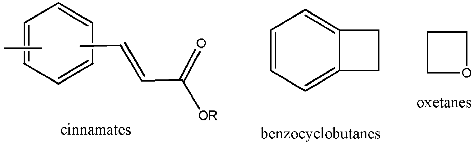

- wherein R in the above structures stands for an alkyl or an alkylene group having from 1 to 20 carbon atoms.
- Organic molecule M2 may be the same as M1 or differ from M1 only in the fact that one or more of the polymerizable units G1 in organic molecule M1 are replaced by polymerizable or non-polymerizable units G2 of formula (5)
-(Z2)a' - (Ph)b' - Oc' - (C(=O))d' - Oe' - A2 (5)
- wherein A2 is chosen from hydrogen, halogen, C1-C20 alkyl groups, halogenated C1-C20 alkyl groups, C2-C20 alkenyl groups, C2-C20 halogenated alkenyl groups, C4-C20 alkadienyl groups, halogenated C4-C20 alkadienyl groups, C4-C20 cycloalkenyl groups or C4-C20 alkylene bridged cycloalkenyl groups, Ph is o-, m- or p-phenylene and Z2 may be selected from the group of compounds defined before for Z1 and a' to e', independent of one another, are 0 or 1.
- M2 may differ from M1. In accordance with a preferred embodiment M1 and M2 are identical.
- M2 as explained above may not comprise a polymerizable unit at all, it may comprise the same polymerizable units as M1 or it may comprise different polymerizable units than M1.
- If M2 comprises different polymerizable units G2 than are present in M1, the G2 units may also be selected from the groups as described hereinbefore for G1.
- The organic molecules M1 and M2 may be selected from a wide variety of compounds and the skilled person will make the appropriate selection for his intended purpose.
- Ambipolar and cross-linkable compounds which have a sufficient solubility in the solvent systems used are generally suitable and respective compounds are known to the skilled person, who will select the appropriate compounds based on his knowledge and in accordance with the needs of the specific application.
- A first group of preferred organic molecules which may be advantageously used in the process in accordance with the present invention are arylamine compounds comprising an arylamine core and at least one polymerizable group attached to one ring of the arylamine core
- These arylamine compounds comprise an arylamine core. When used herein, the term arylamine core generally denotes a structural element where aryl groups are attached to one or more nitrogen atoms.
- Generally, an arylamine core can be depicted as NAr1Ar2Ar3 wherein Ar1, Ar2 and Ar3, which may be the same or different, represent a substituted or unsubstituted C5 to C30 aryl- or a substituted or unsubstituted C2 to C30 hetereoaryl group. Preferred examples of aryl groups are phenyl, naphthyl and anthracenyl, especially phenyl or naphthyl. Preferred heteroaryl groups are five or six membered heteroaryl compounds comprising at least one heteroatom, preferably selected from O, N and S, particularly preferred the heteroaryl ring contains at least one nitrogen atom.
- A first preferred class of arylamine compounds in accordance with the present invention is represented by compounds of general formula (6)

- wherein at least one of A and R8 to R11 carries an addition-polymerizable group attached through a spacer of general formula (1) wherein A can have the same meaning as Ar1 defined above; preferably A is selected from the group consisting of substituted or unsubstituted 5 to 7 membered aryl or heteroaryl rings, n is1, 2 or 3 and R8 to R11, independent of one another, are unsubstituted or substituted C5 to C30 aryl or C2 to C30 heteroaryl rings as defined before for Ar1.
- In accordance with another preferred embodiment, the compounds of the present invention of formula (6) comprise a substituted or unsubstituted phenyl or naphthyl group.
- The addition polymerizable group preferably comprises at least one unsaturated bond which may be polymerized by addition polymerization.
- The polymerizable unit is preferably selected from the group consisting of

- Vinyl groups are generally preferred as polymerizable unit G1 or G2, particularly vinylphenyl (also commonly referred to as styryl or vinylphenyl).
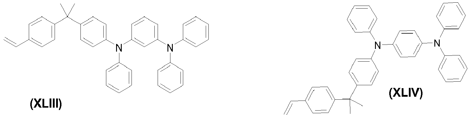
- The following specific examples of arylamine compounds (formulae I to XLIV), individually, can be advantageously used in the present invention, process of the present invention, compounds XVII to XLIV being especially preferred.


- Other suitable organic molecules which may be used as M1 and/or M2 in the process of the present invention, have been described in the literature, i.e. in Zuniga et. al, Chem. Mater. 2011, 23, 658 et seq. to which reference is made herewith.
- As a general rule, any compound known from the prior art which has been described for use in multilayer structures of organic electronic devices may be used, provided modification with a polymerizable group in case of organic molecule M1 is possible.
- The skilled person will select the appropriate organic molecules M1 and M2 depending on the purpose of the layer for which the molecules are used based on his professional skills and knowledge.
- In the first step of the process in accordance with the present invention, a first layer L1 of the desired multilayer structure is deposited onto a substrate out of a liquid composition C1 comprising a solvent system S1 which solvent system S1 comprises the organic material M1.
- The substrate may be a previously deposited layer L0 or it may be an element suitable for forming the anode or cathode of the organic electronic device comprising the multilayer structure.
- Suitable deposition methods are known to the skilled person and described in the literature, to which reference is made herewith for details. The skilled person will use his professional knowledge and select the solution based deposition method suited best for the specific situation.
- Known methods for depositing a material out of a liquid composition are spin coating, spray coating and blade coating to mention only three representative examples.
- In step b of the process in accordance with the present invention, the solubility, measured at 23°C and atmospheric pressure (101.325 kPa),of the layer L1 deposited in step a in the solvent system S2 used for depositing the second layer L2 is reduced by at least 50 %, preferably by at least 70 % and even more preferably by at least 90 %, compared to the solubility of the layer L1 in solvent system S2 before modification.
- The solvent systems S1 and S2 may be the same or different and preferably are the same as this facilitates the process due to the avoidance of intermediate cleaning or solvent change steps or the like if a change of solvent compositions takes place.
- The solvent compositions comprise one or more solvents which are selected to achieve a sufficient solubility of the organic molecules M1 and M2 in the respective solvent systems as this is advantageous for forming a homogenous thin layer.
- Accordingly, the solvent or solvents in the solvent composition will be selected depending on the chemical structure and properties of organic molecules M1 and M2 selected for the specific project.
- Generally, organic solvents will be used in the solvent composition. Although halogenated solvents like fluorinated hydrocarbons are in principle suitable in the process of the present invention, it is preferred to use solvents that are essentially free or entirely free of halogen atoms for safety and environmental reasons. Just by way of example, liquid alkanes, cycloalkanes, aldehydes, ketones, esters, ether or aromatic solvents may be mentioned. In certain deposition methods it may be preferable to use solvent mixtures to adjust the properties of the solvent system to achieve a homogenous thin layer in the deposition process. In this regard it has been shown to be advantageous in certain cases to use solvent mixtures comprising solvents with different boiling temperatures which on one hand provide smooth layers and on the other hand have an evaporation behaviour avoiding premature drying of the solvent composition during deposition which might be detrimental for the efficiency of the multilayer structure. Just by way of example, it may be mentioned here to use solvent combinations comprising a solvent with a boiling point at room temperature of at most 130°C with a solvent having a boiling point above that limit and preferably having a boiling point of at least 150°C, particularly preferably of at least 180°C. All boiling points refer to the boiling points at atmospheric pressure.
- The solvent compositions, in addition to one or more solvents and the organic molecules may also contain further additives and processing aids commonly used in such compositions in solution based processes. These are commercially available and described in the literature and thus no further details are necessary here.
- Zuniga et al., Chem. Mater. 2011, 23, 658 describe the conditions under which the polymerizable units shown above may be polymerized and/or cross-linked to achieve the reduction in solubility.
- For the purpose of this invention cross-linking would be understood as a process whereby the formation of new chemical bonds leads to insolubilization of an organic layer by forming bonds between polymer or oligomer chains.
- The formation of siloxanes with a three dimensional crosslinked network from the hydrolysis of halo- or alkoxysilanes is widely used in materials science. The process can lead to effective cross-linking and the resulting bonds are strong and stable. The hydrolysis step involves generally the exposure of the layer to moisture followed by a curing step at elevated temperature (generally 120°C or above). However, in certain cases the presence of moisture in the system is undesirable as it may be detrimental to the lifetime of the organic electronic device comprising the multilayer structure obtained in accordance with the process of the present invention. The skilled person will decide whether or not siloxanes and their crosslinking using moisture is acceptable or not in his specific situation.
- Styryl groups usually require temperatures of 150°C or above to achieve the desired cross-linking and vinyl ethers and benzocyclobutenes often require even higher temperatures exceeding in many cases 200°C. Treatment of the layer at such elevated temperatures for several hours may be detrimental to the stability and the properties of the layer and thus styryl groups, offering a reasonable compromise of cross-linking temperature and time needed, may be advantageously used in a number of cases.
- The time needed to achieve the desired decrease of solubility may range from a few minutes to several hours and depends on the structure of the respective organic molecule. Typically, reaction times in the range of from 5 minutes to 12 hours, preferably of from 15 minutes to 6 hours at the temperature needed for the respective polymerizable group are appropriate. Thus, e.g. for styryl-type polymerizable group reaction times of from 15 minutes to 6 hours at temperatures in the range of from 120 to 200°C, preferably of from 130 to 180°C have proved to yield the desired results.
- UV-initiated cross-linking can be used for the radical polymerization of acrylates and the cationic polymerization of oxetanes. The radiation wavelength and intensity will be selected by the skilled person dependending on the actual organic molecules used.
- The dimerization and crosslinking of cinnamates and chalcones in most cases occur by direct photooxidation of the polymerizable groups.
- Photochemical processes offer the potential to avoid the high temperatures associated with thermal polymerization, but e.g. in the case of oxetane polymerization a heating step is also sometimes found to be useful to achieve the desired degree of reaction.
- The oxetane and cinnamate/chalcone approaches can be advantageous because these groups are inert under radical polymerization conditions and thus can be readily incorporated as side chains into main chain acrylate or styrene polymers.
- In step c of the process in accordance with the present invention, a second layer L2 of the multilayer structure is deposited onto the first layer out of a liquid composition C2 comprising a solvents system S2 which solvent system comprises art least one organic molecule M2 as defined above.
- According to a preferred embodiment of the present invention, in step c an organic molecule M2 is used which is the same as organic molecule M1.
- If M1 and M2 differ, preferably from 1 to 2 polymerizable units G1 in M1 are replaced by different polymerizable or non-polymerizable units G2 as defined above.
- In cases where the second layer L2 is the last layer of the multilayer device deposited, it may not be necessary to use a monomer with polymerizable units and in this case M2 accordingly preferably does not comprise polymerizable units G2.
- The liquid compositions C1 and C2 comprise the solvent compositions S1 respectively S2, which in turn contain the organic molecules M1 and M2. Besides these components, the liquid compositions C1 and C2 in accordance with the present invention may comprise additives and processing aids generally known to be useful in the deposition processes in steps a and c of the process in accordance with the present invention. The skilled person will select the appropriate additives and processing aids based on his professional knowledge and the circumstances of the specific application situation. Thus, no further details are necessary here.
- In accordance with a preferred embodiment of the process in accordance with the present invention liquid composition C1 or liquid composition C2 or both liquid compositions may comprise at least one organic molecule M3, which may be the same or different in liquid composition C1 and liquid composition C2. Organic molecule M3, similar as organic molecules M1 and M2 has a molecular weight of at most 1000 Dalton, preferably of at most 700 Dalton.
- The core of the organic molecule with M3 is chosen from benzene, pyridine, cyanurate and isocyanurate and the organic molecule M3 attached to its core bears n2 polymerizable groups of formula (7)
-
- Oc" - (C(=O))d" - Oe" - A3 (7)
- wherein n2 is an integer of from 2 to 4 and A3 is vinyl or allyl and c", d" and e", independent of one another are 0 or 1. In accordance with a preferred embodiment A3 is allyl and preferred organic molecules M3 are divinyl benzene, diallyl phthalate, triallylcyanurate and ztriallylcyanurate and mixtures thereof.
- In accordance with the preferred embodiment either one or both liquid compositions comprise an organic molecule M3 and in case said organic molecule M3 is contained in both liquid compositions, preferably that same organic molecule M3 is used.
- Organic molecules M3 through their at least two polymerizable groups provide the opportunity to achieve a cross-linking in the course of the polymerization of organic molecules M1 and/or M2 which do not have more than one polymerizable group and thus will not yield a three-dimensional network with linked oligomer or polymer chains. As outlined hereinbefore, in certain cases the polymers without cross-linking may have a reduced solubility as required. If the reduction of solubility without linking of polymer or oligomer chains is not sufficient, the use of organic molecules M3 will provide the necessary cross-linking.
- The concentration of organic molecules M3, if present, is usually within the range of from 0.1 to 20 mole%, preferably of from 0,5 to 10 mole% of the amount of organic molecule M1 and/or M2.
- The process in accordance with the present invention is particularly suited for the manufacture of multilayer structures which form part of organic electronic devices, in particular organic light emitting diodes.
- Due to the fact that the process uses solution based deposition methods, the amount of material needed for deposition is reduced and therefore economic advantages achieved over e.g. vapour deposition processes.
- Due to the fact that the HOMO levels of the organic molecules M1 and M2 used for depositing the subsequent layers, as well as their LUMO levels, are very similar and in a preferred embodiment identical, certain advantages can be achieved compared to devices where there is a significant difference between either the HOMO levels, or the LUMO levels, or both, of the materials used for the subsequent layers. In principle, the subsequent layers obtained in accordance with that process of the present invention provide a homojunction between the two layers due to the very small difference in HOMO and LUMO levels of the respective layers and thus the advantages associated with homojunctions outlined hereinabove can be achieved with the process in accordance with the present invention.
- The process in accordance with the present invention may be used for forming at least two layers of a multilayer device but it is immediately apparent to the skilled person that the process may be repeatedly carried out to obtain more than two consecutive layers of a multilayer device. The process is thus useful to obtain a multilayer structure wherein all the layers have been obtained by the process in accordance with the present invention or it may be used to obtain only part of the consecutive layers of the multilayer structure with one or more remaining layers being obtainable by other processes, e.g. vapour deposition technologies or the like.
- In accordance with a preferred embodiment all the layers of the device are obtained in accordance with the process of the present invention.
Claims (14)
- A process for the manufacture of a multilayer structure suitable for forming part of an organic electronic device having a cathode and an anode, comprising the steps ofa. depositing a first layer L1 of the multilayer structure onto a substrate out of a liquid composition C1 comprising a solvent system S1 which solvent system S1 contains at least one organic molecule M1 having a molecular weight of at most 1,000 Dalton, wherein the substrate is a previously deposited layer L0 of the multilayer structure or is an element suitable for forming the cathode or the anode of the organic electronic device,b. thereafter chemically modifying the first layer L1 to reduce its solubility, as measured at room temperature (23°C) and atmospheric pressure (101.325 kPa), in a solvent system S2 which is identical to or different from solvent system S1, by at least 50 %, based on the solubility of the first layer L1 in the solvent system S2 before modification andc. thereafter depositing a second layer L2 of the multilayer structure onto the first layer L1 out of a liquid composition C2 comprising the solvent system S2, which solvent system comprises at least one organic molecule M2 having a molecular weight of at most 1,000 Dalton,
wherein
the organic molecule M1 contains n1 polymerizable groups G1 with n1 being an integer of from 1 to 5,
the organic molecule M2, which is identical to M1 or differs from M1 only in that in the organic molecule M2 1 to n1 polymerizable groups G1 have been replaced by polymerizable or non-polymerizable groups G2 which differ from G1, and
wherein the HOMO and LUMO levels of the organic molecule M1 are the same as, or differ by at most 0.2 eV from, respectively, the HOMO and LUMO levels of the organic molecule M2, as measured by cyclic voltammetry in solution. - The process in accordance with claim 1 wherein the polymerizable unit G1 is selected from the group consisting of vinyl ethers, halogenated vinyl ethers, siloxanes, oxetanes, cinnamates, chalcones, acrylates, methacrylates and styryl groups.
- The process in accordance with claim 1 wherein n1 is an integer of from 1 to 5 and the polymerizable unit G1 is represented by general formula (1)
-(Z1)a - (Ph)b - Oc - (C(=O))d - De- A1 (1)
wherein A1 is selected from the group consisting of C2-C20 alkenyl groups, C2-C20 halogenated alkenyl groups, C4-C20 alkadienyl groups, halogenated C4-C20 alkadienyl groups, C4-C20 cycloalkenyl groups or C4-C20 alkylene bridged cycloalkenyl groups, Ph is p-phenylene,
Z1 is selected from the group consisting of formulae (2) to (4)
C(R1R2)-(C(R3R4))m (2)

R1 and R2, independent of one another, each represent hydrogen, halogen, a C1-C8 alkyl group or an aryl group of from 5 to 30 carbon atoms,
R3 and R4, independent of one another, are hydrogen, a C1 to C8 alkyl group or an aryl group of from 5 to 30 carbon atoms and m is an integer of from 0 to 20,
R5 represents hydrogen, C1 to C8-alkyl, or C5 to C30 aryl, and
R6 and R7, independently of one another, represent C1-C8 alkylene or C5 to C30 arylene
and a to e, independently of one another are each 0 or 1, and
in organic molecule M2, 1 to n1 polymerizable units G1 have been replaced by polymerizable or non-polymerizable units G2, different from G1, and represented by general formulae (5)
-(Z2)a' - (Ph)b' - Oc' - (C(=O))d' - Oe' - A2 (5)
wherein A2 is chosen from hydrogen, halogen, C1-C20 alkyl groups, halogenated C1-C20 alkyl groups, C2-C20 alkenyl groups, C2-C20 halogenated alkenyl groups, C4-C20 alkadienyl groups, halogenated C4-C20 alkadienyl groups, C4-C20 cycloalkenyl groups or C4-C20 alkylene bridged cycloalkenyl groups, Ph is o-, m- or p-phenylene, Z2 is selected from the group consisting of groups as defined above for Z1 and a' to e', independently of one another are each 0 or 1. - The process in accordance with at least one of claims 1 to 3 wherein the solvent systems S1 and S2 are identical.
- The process in accordance with at least one of claims 1 to 4 wherein the solubility in step b is reduced by at least 90 %.
- The process in accordance with at least one of claims 1 to 5 wherein the HOMO levels of M1 and M2, and the LUMO levels of M1 and M2, are the same or differ by at most 0.1 eV.
- The process in accordance with at least one of claims 3 to 6 wherein n1 is 2 or 3.
- The process in accordance with at least one of claims 3 to 7 wherein a is 1.
- The process in accordance with any of claims 3 to 8 wherein at least one of b and c is 0.
- The process in accordance with at least one of claims 3 to 9 wherein M2 is identical to M1.
- The process in accordance with at least one of claims 1 to 10, wherein the liquid composition C1 or the liquid composition C2 or both liquid compositions C1 and C2 contain at least one organic molecule M3, which may be the same or different in liquid composition C1 and liquid composition C2, said organic molecule M3 having a molecular weight of at most 1,000 Dalton and having a core chosen from benzene, pyridine, cyanurate and isocyanurate, said core bearing n2 reactive groups of formula (3)
- Oc" - (C(=O))d" - Oe" - A3 (7)
wherein n2 is an integer of from 2 to 4 and A3 is vinyl or allyl and c", d" and e", independent of one another are 0 or 1. - The process in accordance with claim 11 wherein n2 is 2.
- The process in accordance with claim 11 or 12 wherein A3 is allyl.
- The process in accordance with at least one of claims 11 to 13 wherein A3 is selected from divinyl benzene, diallyl phthalate, triallylcyanurate and triallyl isocyanurate or mixtures thereof.
Priority Applications (1)
| Application Number | Priority Date | Filing Date | Title |
|---|---|---|---|
| EP12186861.6A EP2713414A1 (en) | 2012-10-01 | 2012-10-01 | Process for the manufacture of a multilayer structure |
Applications Claiming Priority (1)
| Application Number | Priority Date | Filing Date | Title |
|---|---|---|---|
| EP12186861.6A EP2713414A1 (en) | 2012-10-01 | 2012-10-01 | Process for the manufacture of a multilayer structure |
Publications (1)
| Publication Number | Publication Date |
|---|---|
| EP2713414A1 true EP2713414A1 (en) | 2014-04-02 |
Family
ID=47008377
Family Applications (1)
| Application Number | Title | Priority Date | Filing Date |
|---|---|---|---|
| EP12186861.6A Withdrawn EP2713414A1 (en) | 2012-10-01 | 2012-10-01 | Process for the manufacture of a multilayer structure |
Country Status (1)
| Country | Link |
|---|---|
| EP (1) | EP2713414A1 (en) |
Cited By (1)
| Publication number | Priority date | Publication date | Assignee | Title |
|---|---|---|---|---|
| JP2017531308A (en) * | 2014-08-21 | 2017-10-19 | ダウ グローバル テクノロジーズ エルエルシー | Composition containing benzocyclobutene-substituted carbazole and electronic device comprising the same |
Citations (3)
| Publication number | Priority date | Publication date | Assignee | Title |
|---|---|---|---|---|
| US20100323464A1 (en) * | 2009-06-17 | 2010-12-23 | Universal Display Corporation | Liquid compositions for inkjet printing of organic layers or other uses |
| US7911129B2 (en) | 2005-04-13 | 2011-03-22 | Novaled Ag | Arrangement for an organic pin-type light-emitting diode and method for manufacturing |
| WO2011119162A1 (en) * | 2010-03-25 | 2011-09-29 | Universal Display Corporation | Solution processable doped triarylamine hole injection materials |
-
2012
- 2012-10-01 EP EP12186861.6A patent/EP2713414A1/en not_active Withdrawn
Patent Citations (3)
| Publication number | Priority date | Publication date | Assignee | Title |
|---|---|---|---|---|
| US7911129B2 (en) | 2005-04-13 | 2011-03-22 | Novaled Ag | Arrangement for an organic pin-type light-emitting diode and method for manufacturing |
| US20100323464A1 (en) * | 2009-06-17 | 2010-12-23 | Universal Display Corporation | Liquid compositions for inkjet printing of organic layers or other uses |
| WO2011119162A1 (en) * | 2010-03-25 | 2011-09-29 | Universal Display Corporation | Solution processable doped triarylamine hole injection materials |
Non-Patent Citations (15)
| Title |
|---|
| CAI ET AL., ORGANIC ELECTRONICS, vol. 12, 2011, pages 843 |
| CHAO CAI ET AL: "Efficient Low-Driving-Voltage Blue Phosphorescent Homojunction Organic Light-Emitting Devices", JAPANESE JOURNAL OF APPLIED PHYSICS, THE JAPAN SOCIETY OF APPLIED PHYSICS, JAPAN SOCIETY OF APPLIED PHYSICS, TOKYO; JP, vol. 50, no. 4 - PT1, 1 April 2011 (2011-04-01), pages 40204 - 1, XP001564325, ISSN: 0021-4922, [retrieved on 20110405], DOI: 10.1143/JJAP.50.040204 * |
| CHENGMEI ZHONG ET AL: "Materials and Devices toward Fully Solution Processable Organic Light-Emitting Diodes", CHEMISTRY OF MATERIALS, AMERICAN CHEMICAL SOCIETY, WASHINGTON, DC, US, vol. 23, no. 3, 8 February 2011 (2011-02-08), pages 326 - 340, XP002683467, ISSN: 1520-5002, [retrieved on 20101021], DOI: 10.1021/CM101937P * |
| CHI-YEN LIN ET AL: "A thermally cured 9,9-diarylfluorene-based triaryldiamine polymer displaying high hole mobility and remarkable ambient stability", JOURNAL OF MATERIALS CHEMISTRY, vol. 19, no. 22, 1 January 2009 (2009-01-01), pages 3618 - 3623, XP055055226, ISSN: 0959-9428, DOI: 10.1039/b900977a * |
| GEORGIOS LIAPTSIS ET AL: "Crosslinkable TAPC-Based Hole-Transport Materials for Solution-Processed Organic Light-Emitting Diodes with Reduced Efficiency Roll-Off", ADVANCED FUNCTIONAL MATERIALS, vol. 23, no. 3, 28 August 2012 (2012-08-28), pages 359 - 365, XP055055176, ISSN: 1616-301X, DOI: 10.1002/adfm.201201197 * |
| HARADA ET AL., PHYS. REV. LETT., vol. 94, 2005, pages 036601 |
| HARADA ET AL., PHYS. REVIEW, vol. 77, 2008, pages 195212 |
| HO ET AL., APPL. PHYS. LETT., vol. 85, 2004, pages 4576 |
| LEUNG ET AL., PROC. OF SPIE, vol. 6828, 2007, pages 68280D |
| POMMEREHENE ET AL., ADV. MATER., vol. 7, no. 6, 1995, pages 551 - 554 |
| YEN-JU CHENG ET AL: "Exciplex Electroluminescence Induced by Cross-Linked Hole-Transporting Materials for White Light Polymer Light-Emitting Diodes", MACROMOLECULES, vol. 44, no. 15, 9 August 2011 (2011-08-09), pages 5968 - 5976, XP055055195, ISSN: 0024-9297, DOI: 10.1021/ma2006969 * |
| ZACHARIAS PHILIPP ET AL: "New crosslinkable hole conductors for blue-phosphorescent organic light-emitting diodes", ANGEWANDTE CHEMIE. INTERNATIONAL EDITION, WILEY VCH VERLAG, WEINHEIM, vol. 46, no. 23, 1 January 2007 (2007-01-01), pages 4388 - 4392, XP009127589, ISSN: 1433-7851, DOI: 10.1002/ANIE.200605055 * |
| ZUNIGA ET AL., CHEM. MATER., vol. 23, 2011, pages 658 |
| ZUNIGA ET AL., CHEM. MATER., vol. 23, 2011, pages 658 - 681 |
| ZUNIGA, CHEM. MATER., vol. 23, 2011, pages 658 |
Cited By (1)
| Publication number | Priority date | Publication date | Assignee | Title |
|---|---|---|---|---|
| JP2017531308A (en) * | 2014-08-21 | 2017-10-19 | ダウ グローバル テクノロジーズ エルエルシー | Composition containing benzocyclobutene-substituted carbazole and electronic device comprising the same |
Similar Documents
| Publication | Publication Date | Title |
|---|---|---|
| CN111094465B (en) | Coating composition, organic light emitting diode using the same, and method of manufacturing the same | |
| Zhao et al. | Novel small-molecule electron donor for solution-processed ternary exciplex with 24% external quantum efficiency in organic light-emitting diode | |
| CN109804027B (en) | Ionic compound, coating composition comprising the same, and organic light emitting diode | |
| KR101762964B1 (en) | Charge injection and transport layers | |
| CN102844902B (en) | Compositions and methods for making organic electronic devices | |
| KR101618395B1 (en) | Liquid compositions for inkjet printing of organic layers or other uses | |
| JP2016540381A (en) | Multilayer structure with SBF matrix material in adjacent layers | |
| EP3532566B1 (en) | Formulation of an organic functional material | |
| JP7019559B2 (en) | Compositions containing organic semiconductor compounds | |
| EP2333862B1 (en) | Process for manufacturing organic electroluminescent element | |
| EP1257611A1 (en) | Luminescent polymer | |
| TWI777192B (en) | Compound, coating composition comprising the same, and organic light emitting device using the same | |
| Hellerich et al. | Fluorescent polymer guest: small molecule host solution-processed OLEDs | |
| CN107849016A (en) | Compounds with fluorene structure | |
| JP2019057484A (en) | Organic electroluminescent device, method of manufacturing organic electroluminescent device | |
| KR20190022812A (en) | Formulation of organic functional material | |
| EP3547384B1 (en) | High polymer, mixture containing same, composition, organic electronic component, and monomer for polymerization | |
| Liguori et al. | Study of the electroluminescence of highly stereoregular poly (N-pentenyl-carbazole) for blue and white OLEDs | |
| KR20170134523A (en) | Formulation of an organic functional material comprising a siloxane solvent | |
| CN101675542A (en) | Electric organic component and method for the production thereof | |
| GB2547645A (en) | Compound,composition and organic light-emitting device | |
| JP2009505409A (en) | Solvent mixtures for organic semiconductors | |
| EP2713414A1 (en) | Process for the manufacture of a multilayer structure | |
| TWI813576B (en) | Formulations with a low content of phenol type impurities | |
| CN116584174A (en) | Organic Electroluminescent Device Materials |
Legal Events
| Date | Code | Title | Description |
|---|---|---|---|
| PUAI | Public reference made under article 153(3) epc to a published international application that has entered the european phase |
Free format text: ORIGINAL CODE: 0009012 |
|
| AK | Designated contracting states |
Kind code of ref document: A1 Designated state(s): AL AT BE BG CH CY CZ DE DK EE ES FI FR GB GR HR HU IE IS IT LI LT LU LV MC MK MT NL NO PL PT RO RS SE SI SK SM TR |
|
| AX | Request for extension of the european patent |
Extension state: BA ME |
|
| STAA | Information on the status of an ep patent application or granted ep patent |
Free format text: STATUS: THE APPLICATION IS DEEMED TO BE WITHDRAWN |
|
| 18D | Application deemed to be withdrawn |
Effective date: 20141003 |