EP2710403B1 - Detector diode - Google Patents
Detector diode Download PDFInfo
- Publication number
- EP2710403B1 EP2710403B1 EP11722043.4A EP11722043A EP2710403B1 EP 2710403 B1 EP2710403 B1 EP 2710403B1 EP 11722043 A EP11722043 A EP 11722043A EP 2710403 B1 EP2710403 B1 EP 2710403B1
- Authority
- EP
- European Patent Office
- Prior art keywords
- detector
- semiconductor
- radiation
- base material
- semiconductor base
- Prior art date
- Legal status (The legal status is an assumption and is not a legal conclusion. Google has not performed a legal analysis and makes no representation as to the accuracy of the status listed.)
- Active
Links
Images


Classifications
-
- G—PHYSICS
- G01—MEASURING; TESTING
- G01T—MEASUREMENT OF NUCLEAR OR X-RADIATION
- G01T1/00—Measuring X-radiation, gamma radiation, corpuscular radiation, or cosmic radiation
- G01T1/02—Dosimeters
- G01T1/026—Semiconductor dose-rate meters
-
- G—PHYSICS
- G01—MEASURING; TESTING
- G01T—MEASUREMENT OF NUCLEAR OR X-RADIATION
- G01T1/00—Measuring X-radiation, gamma radiation, corpuscular radiation, or cosmic radiation
- G01T1/16—Measuring radiation intensity
- G01T1/24—Measuring radiation intensity with semiconductor detectors
-
- H—ELECTRICITY
- H10—SEMICONDUCTOR DEVICES; ELECTRIC SOLID-STATE DEVICES NOT OTHERWISE PROVIDED FOR
- H10F—INORGANIC SEMICONDUCTOR DEVICES SENSITIVE TO INFRARED RADIATION, LIGHT, ELECTROMAGNETIC RADIATION OF SHORTER WAVELENGTH OR CORPUSCULAR RADIATION
- H10F39/00—Integrated devices, or assemblies of multiple devices, comprising at least one element covered by group H10F30/00, e.g. radiation detectors comprising photodiode arrays
- H10F39/10—Integrated devices
- H10F39/12—Image sensors
- H10F39/18—Complementary metal-oxide-semiconductor [CMOS] image sensors; Photodiode array image sensors
- H10F39/189—X-ray, gamma-ray or corpuscular radiation imagers
Definitions
- the present invention generally relates to a radiation sensor for use particularly in, but by no means exclusively, in measuring radiation dose in photon or electron fields such as for radiation medicine, including radiotherapy and radiation based diagnosis.
- RT Radiox-ray
- IMRT Intensity Modulated Radiation Therapy
- Traditional RT utilizes radiation beams with homogenous dose distribution in the primary beam.
- the actual dose distribution in the patient tumor is often more or less heterogenic.
- IMRT the dose distribution is optimized to be homogenous in the target. This is accomplished by calculating and delivering the primary beam as a non-flat, intensity modulated beam.
- the tool used to plan and optimize the treatment is a TPS (Treatment Planning System).
- the primary beam is shielded during different time periods for different areas in the field to be treated. This is normally performed by using a MLC (Multi Leaf Collimator) where each individual collimator leaf is controlled separately.
- MLC Multi Leaf Collimator
- a typical MLC have 60-80 pairs of 5mm leafs, wherein each pair is capable of opening a radiation slit of up to 40 cm.
- the treatment delivery was provided in a fixed number of projections.
- PTV Pre Treatment Verification
- the 3D dose distribution in a phantom is calculated using the TPS tools for a specific plan and for a specific patient.
- the phantom doesn't have the same shape and heterogeneities as the patient and thereby the dose distribution will not be the same as in the patient.
- the phantom can be irradiated using the patient specific plan and the dose distribution measured inside the phantom can thereby be compared with the planed dose distribution. If the measured dose distribution in the phantom correlates with the dose distribution in the treatment plan for the phantom, it has been proven that the planned treatment can be given as intended.
- the requirement on the isotropy (measurement dependency on incident angle) might vary. If the phantom is to cover from "head and neck" to pelvis, the requirement on isotropy is somewhat limited due to that the incident angle of the beam is limited to solid angle +/-30 degrees in a 360 degree rotation. If the intended use is to cover also full head including brain; the incident beam might be almost 4 ⁇ , i.e. almost any beam direction. High accuracy measurements will then require even higher demands on the detector system to be isotropic, i.e. directional independent.
- An isotropic detector should also fulfill other requirements such as high spatial resolution, energy independency, dose linearity, dose per pulse linearity, low temperature dependency, stability, high signal/ noise ratio, radiation tolerances, real time measurement, configurable in arrays of detectors and not least cost effect to make them useful in practice.
- part of the chip is active and part of it is inactive (bulk) in the collection of free charges.
- the geometric shape is thereby none uniform around the active part of the chip and the secondary electrons from the surrounding will thereby not be uniform; the creation of the local dose will become directional dependent.
- Secondary electrons that enter the active volume via the bulk silicon respectively directly via e.g. water equivalent surrounding the active volume will create different amounts of secondary electrons and thereby the imparted dose will vary with the incident angle.
- US 2009/0057562 Another attempt to provide an isotropic detector is presented in US 2009/0057562 , where a method, apparatus, and computer program for measuring the dose, dose rate or composition of radiation are disclosed.
- an apparatus for detecting and measuring an ambient unknown radiation field includes a large number of detector chips that are facing in different directions is disclosed.
- the detector presented in US 2009/0057562 may also be impaired with problems related to the symmetry of the detector chips, which, in turn, may lead to a signal response which is not independent of the direction of the incoming radiation.
- isotropic detectors having a signal response which is independent of the direction of the incoming radiation that at the same time fulfill other important requirements, such as high spatial resolution, energy independency, dose linearity, dose per pulse linearity, low temperature dependency, stability, high signal/ noise ratio, radiation tolerances, real time measurement, on a detector system for use in measuring radiation dose in photon or electron fields such as for radiation medicine, including radiotherapy and radiation based diagnosis.
- An object of the present invention is to provide an isotropic detector that fulfills at least some of the following requirements, such as high spatial resolution, energy independency, dose linearity, dose per pulse linearity, low temperature dependency, stability, high signal/noise ratio, radiation tolerances, real time measurement, on a detector system for use in measuring radiation dose in photon or electron fields such as for radiation medicine, including radiotherapy and radiation based diagnosis.
- a semiconductor radiation detector comprising a detector element arranged to receive radiation in at least two-non parallel directions and to produce an output corresponding to the received radiation according to claim 1.
- a semiconductor radiation detector comprising a detector element arranged such that it forms a continuous radiation sensitive portion having surfaces oriented in at least two non-parallel directions.
- the semiconductor radiation detector comprises contact means arranged in connection with the detector element for connecting the detector to external equipment.
- the detector element is arranged such that it forms a continuous radiation sensitive portion having surfaces oriented in at least two perpendicular directions.
- the detector element is arranged such that it forms a continuous radiation sensitive portion having surfaces oriented in three perpendicular directions.
- the semiconductor radiation detector further comprises a semiconductor base material.
- the semiconductor base material is shaped as a polyhedron.
- semiconductor base material is shaped as a cube.
- the semiconductor base material has a spherically-like shape.
- the semiconductor base material has a rhombohedral shape.
- a pn-junction is arranged on all sides of the cube shaped semiconductor base material, rhombic shaped semiconductor base material, or on the spherically-like shaped semiconductor base material to form a diode detector.
- This embodiment of a semiconductor radiation detector is a cubically shaped detector having six radiation sensitive surfaces and thus has a reduced or, in practice, a close to zero directional dependence.
- the detector is manufactured in one of the Si layers of a silicon-on-insulator (SOI) wafer.
- SOI silicon-on-insulator
- FIG. 1a schematically shows the semiconductor radiation detector in cross-section along the line A-A in Fig. 1b
- Fig. 1b schematically shows the semiconductor radiation detector seen the direction of the arrow in Fig. 1a .
- the semiconductor radiation detector 10 includes a cubically shaped p-doped bulk silicon semiconductor base material 12.
- Detector element 13 is provided on the semiconductor base material 12.
- the detector element 13 is n + -doped silicon and is provided as a continuous layer on all six sides of the cubically shaped semiconductor base material 12.
- the semiconductor base material 12 and the detector element 13 together form a cube having a side length a.
- contact means 14 is provided on one side of the cubically shaped semiconductor base material 12.
- a first circular contact pin 15 is provided in contact with the semiconductor base material 12 and is arranged with a diameter D.
- a second square-shaped contact pin 16 is provided in contact with the detector element 13 and is arranged with a side length b.
- the first and second contact pins 15, 16 are made of aluminum.
- an outer radiation transparent protection layer 17 made of silicon-oxide (SiO 2 ) is provided on the detector element 13.
- SiO 2 silicon-oxide
- pn-junctions are formed on all six sides of the cubically shaped semiconductor radiation detector 10.
- the semiconductor radiation detector 10 according to the present invention enables measurements of X-ray radiation with a reduced or even close to zero directional dependence. Further, as the active volume of the detector 10 is symmetrically distributed in three dimensions, the lateral extension of the detector can be reduced, which inter alia results in an increased number of detectors per wafer area.
- FIG. 2a schematically shows the semiconductor radiation detector in cross-section along the line B-B in Fig. 2b
- Fig. 2b schematically shows the semiconductor radiation detector seen from the direction of the arrow C in Fig. 2a .
- the semiconductor radiation detector 100 includes a spherically-like shaped p-doped bulk silicon semiconductor base material 102 or a semiconductor base material 102 having cube-like structure with rounded edges and corners.
- a detector element 103 is provided on the semiconductor base material 102.
- the detector element 103 is n + -doped silicon and is provided as a continuous layer on the spherically shaped semiconductor base material 102.
- the semiconductor base material 102 and the detector element 103 form a sphere-like structure or cube-like structure with rounded edges.
- contact means 104 is provided on the detector 100.
- a first circular contact pin 105 is provided in contact with the semiconductor base material 102 and is arranged with a diameter D 1 .
- a second square-shaped contact pin 106 is provided in contact with the detector element 103 and is arranged with a side length b.
- the first and second contact pins 105, 106 are made of aluminum. Moreover, an outer radiation transparent protection layer 107 made of silicon-oxide (SiO 2 ) is provided on the detector element 103. Hence, a pn-junction is formed on the spherically-like semiconductor radiation detector 100.
- the semiconductor radiation detector 100 according to the present invention enables measurements of X-ray radiation with a reduced or even close to zero directional dependence. Further, as the active volume of the detector 100 is symmetrically distributed in three dimensions, the lateral extension of the detector can be reduced, which inter alia results in an increased number of detectors per wafer area.
- the semiconductor radiation detector includes a spherical-like detector element in a cube-like detector.
- the detector element is, for example, n + -doped silicon and is provided as a continuous active volume.
- the detector element 203 is, in this embodiment, substantially circular but may also be, for example, ellipsoidal.
- the detector 200 is cube-shaped and includes p-doped bulk silicon semiconductor base material regions 202 in the corners.
- Contact means 214 is arranged for connection to external equipment including contact pins made of aluminum may be provided on the detector.
- a first contact pin 205 may be arranged close to a semiconductor base material region 202 in one of the corners of the detector 200 in contact with the detector element 203 and a second contact pin 206 may be arranged in contact with the spherically shaped active region of the detector 200.
- an outer radiation transparent protection layer 217 made of silicon-oxide (SiO 2 ) may be provided on the detector element.
- the continuous active volume may have a cube-like shape, an ellipsoidal shape, a cylindrical shape, a spherical shape, or a pyramid-like shape. However, other geometrical shapes are conceivable.
Landscapes
- Health & Medical Sciences (AREA)
- Physics & Mathematics (AREA)
- Life Sciences & Earth Sciences (AREA)
- General Physics & Mathematics (AREA)
- High Energy & Nuclear Physics (AREA)
- Molecular Biology (AREA)
- Spectroscopy & Molecular Physics (AREA)
- Measurement Of Radiation (AREA)
- Toxicology (AREA)
Description
- The present invention generally relates to a radiation sensor for use particularly in, but by no means exclusively, in measuring radiation dose in photon or electron fields such as for radiation medicine, including radiotherapy and radiation based diagnosis.
- Cancer therapy utilizing external high energy x-ray, RT (Radiation Therapy), has developed extensively since the introduction of IMRT (Intensity Modulated Radiation Therapy). Traditional RT utilizes radiation beams with homogenous dose distribution in the primary beam. However, due to variations in beam attenuation across the field caused by irregular shape of the patient anatomy and variation in tissue composition, the actual dose distribution in the patient tumor is often more or less heterogenic. In IMRT the dose distribution is optimized to be homogenous in the target. This is accomplished by calculating and delivering the primary beam as a non-flat, intensity modulated beam. The tool used to plan and optimize the treatment is a TPS (Treatment Planning System).
- To create the intensity modulated beam, the primary beam is shielded during different time periods for different areas in the field to be treated. This is normally performed by using a MLC (Multi Leaf Collimator) where each individual collimator leaf is controlled separately. A typical MLC have 60-80 pairs of 5mm leafs, wherein each pair is capable of opening a radiation slit of up to 40 cm.
- In the first generation of method for intensity modulated treatment, the treatment delivery was provided in a fixed number of projections. In each projection, either a number of fixed fields with different shapes where provided to create the Intensity Modulated field, so called "step and shoot", or, alternatively, the MLC-leafs were moved when the beam was ON, so called "sliding window".
- The introduction of fixed-projection IMRT improved the treatment results compared to previous fixed field technique but the trade-off was significantly increased treatment time and more time was thereby needed to treat each individual patient, which also increased the costs involved in treatment significantly.
- Additionally the creation of the intensity modulated fields increased the treatment complexity and new QC (Quality Control) was required to make sure the treatment was given in accordance with the plan created with the TPS. The QC method PTV, "Pre Treatment Verification", was therefore introduced. In PTV, the 3D dose distribution in a phantom (patient substitution) is calculated using the TPS tools for a specific plan and for a specific patient. The phantom doesn't have the same shape and heterogeneities as the patient and thereby the dose distribution will not be the same as in the patient. However, the phantom can be irradiated using the patient specific plan and the dose distribution measured inside the phantom can thereby be compared with the planed dose distribution. If the measured dose distribution in the phantom correlates with the dose distribution in the treatment plan for the phantom, it has been proven that the planned treatment can be given as intended.
- The ideal phantom would be similar to the patient in shape and density with detectors in the full 3D volume. That is currently not possible due to costs etc. To measure inside the real patient would require a large number of measurement points which is not feasible either. A technique that optimizes the detector configuration in relation to the requirements is described in the US patent
US 7,371,007 . - Depending on the intended use for such a phantom, the requirement on the isotropy (measurement dependency on incident angle) might vary. If the phantom is to cover from "head and neck" to pelvis, the requirement on isotropy is somewhat limited due to that the incident angle of the beam is limited to solid angle +/-30 degrees in a 360 degree rotation. If the intended use is to cover also full head including brain; the incident beam might be almost 4π, i.e. almost any beam direction. High accuracy measurements will then require even higher demands on the detector system to be isotropic, i.e. directional independent.
- An isotropic detector should also fulfill other requirements such as high spatial resolution, energy independency, dose linearity, dose per pulse linearity, low temperature dependency, stability, high signal/ noise ratio, radiation tolerances, real time measurement, configurable in arrays of detectors and not least cost effect to make them useful in practice.
- In a first approximation, for a detector that is small compared to the range of the secondary electron that creates the dose (energy per mass), most of the dose detected by the detector originate from electrons generated outside the detector itself and enters the active volume and deposit the dose. If the surrounding material of the small detection volume is inhomogeneous, the generation of the secondary electrons will depend on the mass density and electron density of the surrounding materials and if it varies the detector will not be isotropic, thereby it is important to have a homogeneous or symmetric surrounding of the detector volume.
- In a traditional diode-detector-chip part of the chip is active and part of it is inactive (bulk) in the collection of free charges. The geometric shape is thereby none uniform around the active part of the chip and the secondary electrons from the surrounding will thereby not be uniform; the creation of the local dose will become directional dependent.
- Secondary electrons that enter the active volume via the bulk silicon respectively directly via e.g. water equivalent surrounding the active volume will create different amounts of secondary electrons and thereby the imparted dose will vary with the incident angle.
- Attempts to provide isotropic detectors have been made, in the early 1990's a double chip (sandwich) detector was constructed to reduce the effect mentioned above. The sandwich detector was more isotropic than a single chip detector but is however impaired with drawbacks. For example, the construction requires that the active part is symmetrically placed in relation to the bulk-silicon and symmetric in shape which, for example, makes it difficult to manufacture. These geometrical asymmetries may lead to a signal response which is not independent of the direction of the incoming radiation.
- Another issue in detectors where the density differs from the surrounding material is energy dependency. The attenuation of low energy (<200keV) photons is for example up to 7 times higher than in water, which leads to an energy dependency in a sandwich construction being more pronounced than in a single chip detector where almost 50% of the surface is facing the surrounding material. Another semiconductor radiation detector is known from
US 4 214 253 . This document discloses a semiconductor radiation detector comprising a detector element with a continuous radiation sensitive pn junction. - Another attempt to provide an isotropic detector is presented in
US 2009/0057562 , where a method, apparatus, and computer program for measuring the dose, dose rate or composition of radiation are disclosed. In one embodiment, an apparatus for detecting and measuring an ambient unknown radiation field includes a large number of detector chips that are facing in different directions is disclosed. However, the detector presented inUS 2009/0057562 may also be impaired with problems related to the symmetry of the detector chips, which, in turn, may lead to a signal response which is not independent of the direction of the incoming radiation. - Thus, there is still a need within the art for isotropic detectors having a signal response which is independent of the direction of the incoming radiation that at the same time fulfill other important requirements, such as high spatial resolution, energy independency, dose linearity, dose per pulse linearity, low temperature dependency, stability, high signal/ noise ratio, radiation tolerances, real time measurement, on a detector system for use in measuring radiation dose in photon or electron fields such as for radiation medicine, including radiotherapy and radiation based diagnosis.
- An object of the present invention is to provide an isotropic detector that fulfills at least some of the following requirements, such as high spatial resolution, energy independency, dose linearity, dose per pulse linearity, low temperature dependency, stability, high signal/noise ratio, radiation tolerances, real time measurement, on a detector system for use in measuring radiation dose in photon or electron fields such as for radiation medicine, including radiotherapy and radiation based diagnosis.
- Further objects and advantages of the present invention will be discussed below by means of exemplifying embodiments.
- This and other features, aspects and advantages of the invention will be more fully understood when considered with respect to the following detailed description, appended claims and accompanying drawings.
- According to an aspect of the present invention, there is provided a semiconductor radiation detector comprising a detector element arranged to receive radiation in at least two-non parallel directions and to produce an output corresponding to the received radiation according to claim 1.
- According to embodiments of the present invention, there is provided a semiconductor radiation detector comprising a detector element arranged such that it forms a continuous radiation sensitive portion having surfaces oriented in at least two non-parallel directions.
- In embodiments of the present invention, the semiconductor radiation detector comprises contact means arranged in connection with the detector element for connecting the detector to external equipment.
- According to embodiments of the present invention, the detector element is arranged such that it forms a continuous radiation sensitive portion having surfaces oriented in at least two perpendicular directions.
- In embodiments of the present invention, the detector element is arranged such that it forms a continuous radiation sensitive portion having surfaces oriented in three perpendicular directions.
- According to the present invention, the semiconductor radiation detector further comprises a semiconductor base material.
- According to embodiments of the present invention, the semiconductor base material is shaped as a polyhedron.
- According to embodiments of the present invention, semiconductor base material is shaped as a cube.
- In further embodiments of the present invention, the semiconductor base material has a spherically-like shape.
- According to embodiments of the present invention, the semiconductor base material has a rhombohedral shape.
- Furthermore, according to embodiments of the present invention, a pn-junction is arranged on all sides of the cube shaped semiconductor base material, rhombic shaped semiconductor base material, or on the spherically-like shaped semiconductor base material to form a diode detector.
- Further objects and advantages of the present invention will be discussed below by means of exemplifying embodiments.
- These and other features, aspects and advantages of the invention will be more fully understood when considered with respect to the following detailed description, appended claims and accompanying drawings.
- Exemplifying embodiments of the invention are illustrated by way of example and not by way of limitation in the figures of the accompanying drawings in which like references indicate similar elements. It should be noted that references to "an" or "one" embodiment in this discussion are not necessarily to the same embodiment, and such references mean at least one.
-
Fig. 1a schematically shows a cross-sectional view of an embodiment of a semiconductor radiation detector according the present invention; -
Fig 1b schematically shows the semiconductor radiation detector according the present invention shown inFig. 1a from a different view; -
Fig. 2a schematically shows a cross-sectional view of an embodiment of a semiconductor radiation detector according the present invention; -
Fig 2b schematically shows the semiconductor radiation detector according the present invention shown inFig. 2a from a different view -
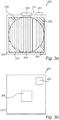
Fig. 3a schematically shows an example of a semiconductor radiation detector; and -
Fig 3b schematically shows the semiconductor radiation detector shown inFig. 3a from a different view. - The following is a description of exemplifying embodiments in accordance with the present invention. This description is not to be taken in limiting sense, but is made merely for the purposes of describing the general principles of the invention. It is to be understood that other embodiments may be utilized and structural and logical changes may be made without departing from the scope of the present invention as defined by the appended claims.
- First, an example process for manufacturing a semiconductor radiation detector according to an embodiment not covered by the present invention will be briefly
described. This embodiment of a semiconductor radiation detector is a cubically shaped detector having six radiation sensitive surfaces and thus has a reduced or, in practice, a close to zero directional dependence. In this example process, the detector is manufactured in one of the Si layers of a silicon-on-insulator (SOI) wafer. This example process involves particularly: - Creating four vertical surfaces by deep reactive ion etching of trenches through one of the Si layers of the SOI wafer, with the buried oxide acting as on etch-stop. The vertical surfaces as well as the top surface are doped from a gaseous source at elevated temperatures. Gaseous diffusion down through the trenches enables doping of vertical surfaces.
- Re-filling the trenches by deposition of one or more thin film layers to preserve the mechanical integrity of the wafer and to create a planar surface for subsequent processing.
- Etching away the second Si layer of the SOI wafer which has acted as a carrier. The re-filled trenches entails that the remaining wafer is held together without the carrier. After this step, the sixth surface of the cubic chip is exposed and is doped, e.g. by ion implantation. Metallization, passivation and chip dicing may then be carried out by conventional processing.
- With reference to
Fig. 1a and 1b , an embodiment of the detector according to the present invention, which can be fabricated using the principles described above, will be discussed.Fig. 1a schematically shows the semiconductor radiation detector in cross-section along the line A-A inFig. 1b and Fig. 1b schematically shows the semiconductor radiation detector seen the direction of the arrow inFig. 1a . - The
semiconductor radiation detector 10 according to this specific embodiment includes a cubically shaped p-doped bulk siliconsemiconductor base material 12.Detector element 13 is provided on thesemiconductor base material 12. Thedetector element 13 is n+-doped silicon and is provided as a continuous layer on all six sides of the cubically shapedsemiconductor base material 12. Thesemiconductor base material 12 and thedetector element 13 together form a cube having a side length a. - Furthermore, contact means 14 is provided on one side of the cubically shaped
semiconductor base material 12. In this embodiment, a firstcircular contact pin 15 is provided in contact with thesemiconductor base material 12 and is arranged with a diameter D. A second square-shapedcontact pin 16 is provided in contact with thedetector element 13 and is arranged with a side length b. - In this embodiment of the present invention, the first and second contact pins 15, 16 are made of aluminum. Moreover, an outer radiation
transparent protection layer 17 made of silicon-oxide (SiO2) is provided on thedetector element 13. Hence, pn-junctions are formed on all six sides of the cubically shapedsemiconductor radiation detector 10. Thesemiconductor radiation detector 10 according to the present invention enables measurements of X-ray radiation with a reduced or even close to zero directional dependence. Further, as the active volume of thedetector 10 is symmetrically distributed in three dimensions, the lateral extension of the detector can be reduced, which inter alia results in an increased number of detectors per wafer area. - With reference now to
Fig. 2a and 2b , another embodiment of a semiconductor radiation detector according to the present invention will be discussed.Fig. 2a schematically shows the semiconductor radiation detector in cross-section along the line B-B inFig. 2b and Fig. 2b schematically shows the semiconductor radiation detector seen from the direction of the arrow C inFig. 2a . - The semiconductor radiation detector 100 according to this specific embodiment includes a spherically-like shaped p-doped bulk silicon
semiconductor base material 102 or asemiconductor base material 102 having cube-like structure with rounded edges and corners. Adetector element 103 is provided on thesemiconductor base material 102. Thedetector element 103 is n+-doped silicon and is provided as a continuous layer on the spherically shapedsemiconductor base material 102. Thesemiconductor base material 102 and thedetector element 103 form a sphere-like structure or cube-like structure with rounded edges. - Furthermore, contact means 104 is provided on the detector 100. In this embodiment, a first
circular contact pin 105 is provided in contact with thesemiconductor base material 102 and is arranged with a diameter D1. A second square-shapedcontact pin 106 is provided in contact with thedetector element 103 and is arranged with a side length b. - In this embodiment of the present invention, the first and second contact pins 105, 106 are made of aluminum. Moreover, an outer radiation
transparent protection layer 107 made of silicon-oxide (SiO2) is provided on thedetector element 103. Hence, a pn-junction is formed on the spherically-like semiconductor radiation detector 100. The semiconductor radiation detector 100 according to the present invention enables measurements of X-ray radiation with a reduced or even close to zero directional dependence. Further, as the active volume of the detector 100 is symmetrically distributed in three dimensions, the lateral extension of the detector can be reduced, which inter alia results in an increased number of detectors per wafer area. - According to a further example of a detector shown in
Figs. 3a and 3b , though not being within the scope of the invention, the semiconductor radiation detector includes a spherical-like detector element in a cube-like detector. The detector element is, for example, n+-doped silicon and is provided as a continuous active volume. Thedetector element 203 is, in this embodiment, substantially circular but may also be, for example, ellipsoidal. Thedetector 200 is cube-shaped and includes p-doped bulk silicon semiconductorbase material regions 202 in the corners. Contact means 214 is arranged for connection to external equipment including contact pins made of aluminum may be provided on the detector. For example, afirst contact pin 205 may be arranged close to a semiconductorbase material region 202 in one of the corners of thedetector 200 in contact with thedetector element 203 and asecond contact pin 206 may be arranged in contact with the spherically shaped active region of thedetector 200. Moreover, an outer radiationtransparent protection layer 217 made of silicon-oxide (SiO2) may be provided on the detector element. The continuous active volume may have a cube-like shape, an ellipsoidal shape, a cylindrical shape, a spherical shape, or a pyramid-like shape. However, other geometrical shapes are conceivable. - Although certain embodiments and examples have been described herein, it will be understood by those skilled in the art that many aspects of the devices and methods shown and described in the present disclosure may be differently combined and/or modified to form still further embodiments. Alternative embodiments and/or uses of the devices and methods described above and obvious modifications and equivalents thereof are intended to be within the scope of the present disclosure. Thus, it is intended that the scope of the present invention should not be limited by the particular embodiments described above, but should be determined by a fair reading of the claims that follow.
Claims (8)
- A semiconductor radiation detector comprising a detector element (13) arranged to receive radiation in at least two non-parallel directions and to produce an output corresponding to the received radiation, wherein the detector (10) comprises a three-dimensional semiconductor base material (12), wherein said detector element is arranged such that it forms a continuous radiation sensitive pn-junction with the semiconductor base material, wherein the detector element is provided on all sides of the semiconductor base material, and wherein the detector further comprises a first contact (15) being in contact with a semiconductor base material region and a second contact (16) being in contact with the detector element.
- The semiconductor radiation detector according to claim 1, wherein said detector element (13) is arranged such that it has surfaces oriented in at least two perpendicular directions.
- The semiconductor radiation detector according to any one of the preceding claims, wherein said detector element (13) is arranged such that it has surfaces oriented in three perpendicular directions.
- The semiconductor radiation detector according to any one of the preceding claims, wherein said semiconductor base material (12) has a polyhedral shape.
- The semiconductor radiation detector according to any one of the preceding clams, wherein said semiconductor base material (12) is shaped as a cube.
- The semiconductor radiation detector according to any one of claims 1 to 4, wherein said semiconductor base material (102) has a spherically-like shape.
- The semiconductor radiation detector according to any one of claims 1 to 4, wherein said semiconductor base material (12) has a rhombohedron shape.
- The semiconductor radiation detector according to any one of preceding claims 5 to 7, wherein the pn-junction is formed on all sides of said polyhedral semiconductor base material (12).
Applications Claiming Priority (1)
| Application Number | Priority Date | Filing Date | Title |
|---|---|---|---|
| PCT/EP2011/058264 WO2012159648A1 (en) | 2011-05-20 | 2011-05-20 | Detector diode |
Publications (2)
| Publication Number | Publication Date |
|---|---|
| EP2710403A1 EP2710403A1 (en) | 2014-03-26 |
| EP2710403B1 true EP2710403B1 (en) | 2020-02-19 |
Family
ID=44119169
Family Applications (1)
| Application Number | Title | Priority Date | Filing Date |
|---|---|---|---|
| EP11722043.4A Active EP2710403B1 (en) | 2011-05-20 | 2011-05-20 | Detector diode |
Country Status (4)
| Country | Link |
|---|---|
| US (1) | US9778373B2 (en) |
| EP (1) | EP2710403B1 (en) |
| CN (1) | CN103703390A (en) |
| WO (1) | WO2012159648A1 (en) |
Families Citing this family (2)
| Publication number | Priority date | Publication date | Assignee | Title |
|---|---|---|---|---|
| CN108428329B (en) * | 2018-02-02 | 2023-05-12 | 江苏艾科半导体有限公司 | Portable detection alarm device for packaging tray of integrated circuit IC |
| EP3909234A4 (en) * | 2019-01-10 | 2022-06-15 | Shenzhen Xpectvision Technology Co., Ltd. | Image sensor having radiation detectors of different orientations |
Family Cites Families (18)
| Publication number | Priority date | Publication date | Assignee | Title |
|---|---|---|---|---|
| US3427454A (en) * | 1965-12-23 | 1969-02-11 | Webb James E | Biomedical radiation detecting probe |
| JPS5536953B2 (en) * | 1974-11-30 | 1980-09-25 | ||
| US4214253A (en) * | 1977-06-13 | 1980-07-22 | General Electric Company | Radiation detector |
| US4207518A (en) * | 1978-03-06 | 1980-06-10 | General Microwave Corporation | Broadband radiation detector with diode elements |
| DE3941706C1 (en) * | 1989-12-18 | 1991-02-28 | Gesellschaft Fuer Strahlen- Und Umweltforschung Mbh, 8042 Neuherberg, De | |
| IL96623A0 (en) * | 1989-12-26 | 1991-09-16 | Gen Electric | Low capacitance,large area semiconductor photodetector and photodetector system |
| US6046454A (en) * | 1995-10-13 | 2000-04-04 | Digirad Corporation | Semiconductor radiation detector with enhanced charge collection |
| US6037595A (en) | 1995-10-13 | 2000-03-14 | Digirad Corporation | Radiation detector with shielding electrode |
| US5698857A (en) * | 1995-12-19 | 1997-12-16 | Eastman Kodak Company | (Barium hafnate: Cu) phosphors and phosphor screens |
| US6614025B2 (en) * | 2000-03-28 | 2003-09-02 | Thomson & Nielsen Electronics Ltd. | Radiation sensor and dosimeter incorporating same |
| JP3900992B2 (en) * | 2002-04-02 | 2007-04-04 | 株式会社日立製作所 | Radiation detector and radiation inspection apparatus |
| SE0301508D0 (en) | 2003-05-23 | 2003-05-23 | Goergen Nilsson | Method of pre-treatment verification in intensity modulates radiation therapy |
| JP2007127607A (en) | 2005-11-07 | 2007-05-24 | Mitsutoyo Corp | Sensor block |
| US20120132814A1 (en) * | 2007-02-26 | 2012-05-31 | Irving Weinberg | Radiation detection device, system and related methods |
| EP2130063B1 (en) | 2007-03-09 | 2017-10-18 | European Organisation for Nuclear Research CERN | Method, apparatus and computer program for measuring the dose, dose rate or composition of radiation |
| US9557635B2 (en) * | 2007-10-18 | 2017-01-31 | Gearbox, Llc | Ionizing-radiation-responsive compositions, methods, and systems |
| IL189254A0 (en) * | 2008-02-04 | 2008-08-07 | Garber Valery | Quantum uncooled infra-red photo-detector |
| US8039790B2 (en) * | 2009-05-14 | 2011-10-18 | University Health Network | Phantoms and methods for verification in radiotherapy systems |
-
2011
- 2011-05-20 EP EP11722043.4A patent/EP2710403B1/en active Active
- 2011-05-20 WO PCT/EP2011/058264 patent/WO2012159648A1/en not_active Ceased
- 2011-05-20 US US14/118,031 patent/US9778373B2/en active Active
- 2011-05-20 CN CN201180070848.6A patent/CN103703390A/en active Pending
Non-Patent Citations (1)
| Title |
|---|
| None * |
Also Published As
| Publication number | Publication date |
|---|---|
| WO2012159648A1 (en) | 2012-11-29 |
| CN103703390A (en) | 2014-04-02 |
| US20140091413A1 (en) | 2014-04-03 |
| US9778373B2 (en) | 2017-10-03 |
| EP2710403A1 (en) | 2014-03-26 |
Similar Documents
| Publication | Publication Date | Title |
|---|---|---|
| Rosenfeld | Novel detectors for silicon based microdosimetry, their concepts and applications | |
| US12019194B2 (en) | Structured detectors and detector systems for radiation imaging | |
| US10712455B2 (en) | Structured detectors and detector systems for radiation imaging | |
| US8421022B2 (en) | Method and apparatus for tissue equivalent solid state microdosimetry | |
| US6528795B2 (en) | Compton scatter imaging instrument | |
| Tran et al. | 3D-Mesa “Bridge” Silicon Microdosimeter: Charge Collection Study and Application to RBE Studies in $^{12}{\rm C} $ Radiation Therapy | |
| US9941440B2 (en) | Radiation microdosimeters correlated with biological cells and cell components | |
| Mackin et al. | The effects of Doppler broadening and detector resolution on the performance of three‐stage Compton cameras | |
| Petasecca et al. | Angular independent silicon detector for dosimetry in external beam radiotherapy | |
| Bläckberg et al. | Light spread manipulation in scintillators using laser induced optical barriers | |
| US9778373B2 (en) | Detector diode | |
| Zahradnik et al. | A diamond guard ring microdosimeter for ion beam therapy | |
| Zhang et al. | Design and performance evaluation of a BGO+ SiPM detector for high-energy prompt gamma imaging in proton therapy monitoring | |
| WO2017017417A1 (en) | Microdosimeter comprising an inductive superconducting transition edge sensor | |
| Domingo-Pardo et al. | A novel γ‐ray imaging method for the pulse-shape characterization of position sensitive semiconductor radiation detectors | |
| Goel et al. | Spatial calibration via imaging techniques of a novel scanning system for the pulse shape characterisation of position sensitive HPGe detectors | |
| Norlin et al. | A cubic isotropic X-ray dose detector diode fabricated by DRIE of SOI substrates | |
| Alhujaili et al. | Characterization of an “edgeless” dosimeter for angular independent measurements in advanced radiotherapy treatments | |
| CN108333620A (en) | The localization method of detection device and middle low energy gamma source | |
| WO2012138792A1 (en) | Annular-array type beam-position monitor with sub-micron resolution and a parametric method for optimizing photo detectors | |
| Yamaguchi et al. | Imaging of therapeutic carbon-ion beams in a human-head phantom measuring prompt X-rays | |
| Jelinek et al. | Evaluation of Timepix3 with a 1 mm thick silicon sensor as a Compton imaging polarimeter in the hard X-ray band | |
| Granja et al. | Spatial Dosimetry Verification of Conformal Beams in Proton Radiotherapy by Spectral-Sensitive Imaging | |
| US9759672B2 (en) | Radiation detecting wearable devices | |
| McCann et al. | Performance and Inter-Comparison of Novel 4π-Optimized Compton Imagers |
Legal Events
| Date | Code | Title | Description |
|---|---|---|---|
| PUAI | Public reference made under article 153(3) epc to a published international application that has entered the european phase |
Free format text: ORIGINAL CODE: 0009012 |
|
| 17P | Request for examination filed |
Effective date: 20131107 |
|
| AK | Designated contracting states |
Kind code of ref document: A1 Designated state(s): AL AT BE BG CH CY CZ DE DK EE ES FI FR GB GR HR HU IE IS IT LI LT LU LV MC MK MT NL NO PL PT RO RS SE SI SK SM TR |
|
| DAX | Request for extension of the european patent (deleted) | ||
| STAA | Information on the status of an ep patent application or granted ep patent |
Free format text: STATUS: EXAMINATION IS IN PROGRESS |
|
| 17Q | First examination report despatched |
Effective date: 20161220 |
|
| GRAP | Despatch of communication of intention to grant a patent |
Free format text: ORIGINAL CODE: EPIDOSNIGR1 |
|
| STAA | Information on the status of an ep patent application or granted ep patent |
Free format text: STATUS: GRANT OF PATENT IS INTENDED |
|
| INTG | Intention to grant announced |
Effective date: 20190930 |
|
| RIN1 | Information on inventor provided before grant (corrected) |
Inventor name: NILSSON, GOERGEN Inventor name: NORLIN, PETER Inventor name: KAPLAN, WLODEK Inventor name: JUNIQUE, STEPHANE |
|
| GRAS | Grant fee paid |
Free format text: ORIGINAL CODE: EPIDOSNIGR3 |
|
| GRAA | (expected) grant |
Free format text: ORIGINAL CODE: 0009210 |
|
| STAA | Information on the status of an ep patent application or granted ep patent |
Free format text: STATUS: THE PATENT HAS BEEN GRANTED |
|
| AK | Designated contracting states |
Kind code of ref document: B1 Designated state(s): AL AT BE BG CH CY CZ DE DK EE ES FI FR GB GR HR HU IE IS IT LI LT LU LV MC MK MT NL NO PL PT RO RS SE SI SK SM TR |
|
| REG | Reference to a national code |
Ref country code: GB Ref legal event code: FG4D |
|
| REG | Reference to a national code |
Ref country code: CH Ref legal event code: EP |
|
| REG | Reference to a national code |
Ref country code: DE Ref legal event code: R096 Ref document number: 602011065080 Country of ref document: DE |
|
| REG | Reference to a national code |
Ref country code: AT Ref legal event code: REF Ref document number: 1235600 Country of ref document: AT Kind code of ref document: T Effective date: 20200315 |
|
| REG | Reference to a national code |
Ref country code: IE Ref legal event code: FG4D |
|
| REG | Reference to a national code |
Ref country code: NL Ref legal event code: MP Effective date: 20200219 |
|
| PG25 | Lapsed in a contracting state [announced via postgrant information from national office to epo] |
Ref country code: RS Free format text: LAPSE BECAUSE OF FAILURE TO SUBMIT A TRANSLATION OF THE DESCRIPTION OR TO PAY THE FEE WITHIN THE PRESCRIBED TIME-LIMIT Effective date: 20200219 Ref country code: FI Free format text: LAPSE BECAUSE OF FAILURE TO SUBMIT A TRANSLATION OF THE DESCRIPTION OR TO PAY THE FEE WITHIN THE PRESCRIBED TIME-LIMIT Effective date: 20200219 Ref country code: NO Free format text: LAPSE BECAUSE OF FAILURE TO SUBMIT A TRANSLATION OF THE DESCRIPTION OR TO PAY THE FEE WITHIN THE PRESCRIBED TIME-LIMIT Effective date: 20200519 |
|
| REG | Reference to a national code |
Ref country code: LT Ref legal event code: MG4D |
|
| PG25 | Lapsed in a contracting state [announced via postgrant information from national office to epo] |
Ref country code: HR Free format text: LAPSE BECAUSE OF FAILURE TO SUBMIT A TRANSLATION OF THE DESCRIPTION OR TO PAY THE FEE WITHIN THE PRESCRIBED TIME-LIMIT Effective date: 20200219 Ref country code: GR Free format text: LAPSE BECAUSE OF FAILURE TO SUBMIT A TRANSLATION OF THE DESCRIPTION OR TO PAY THE FEE WITHIN THE PRESCRIBED TIME-LIMIT Effective date: 20200520 Ref country code: BG Free format text: LAPSE BECAUSE OF FAILURE TO SUBMIT A TRANSLATION OF THE DESCRIPTION OR TO PAY THE FEE WITHIN THE PRESCRIBED TIME-LIMIT Effective date: 20200519 Ref country code: SE Free format text: LAPSE BECAUSE OF FAILURE TO SUBMIT A TRANSLATION OF THE DESCRIPTION OR TO PAY THE FEE WITHIN THE PRESCRIBED TIME-LIMIT Effective date: 20200219 Ref country code: LV Free format text: LAPSE BECAUSE OF FAILURE TO SUBMIT A TRANSLATION OF THE DESCRIPTION OR TO PAY THE FEE WITHIN THE PRESCRIBED TIME-LIMIT Effective date: 20200219 Ref country code: IS Free format text: LAPSE BECAUSE OF FAILURE TO SUBMIT A TRANSLATION OF THE DESCRIPTION OR TO PAY THE FEE WITHIN THE PRESCRIBED TIME-LIMIT Effective date: 20200619 |
|
| PG25 | Lapsed in a contracting state [announced via postgrant information from national office to epo] |
Ref country code: NL Free format text: LAPSE BECAUSE OF FAILURE TO SUBMIT A TRANSLATION OF THE DESCRIPTION OR TO PAY THE FEE WITHIN THE PRESCRIBED TIME-LIMIT Effective date: 20200219 |
|
| PG25 | Lapsed in a contracting state [announced via postgrant information from national office to epo] |
Ref country code: SK Free format text: LAPSE BECAUSE OF FAILURE TO SUBMIT A TRANSLATION OF THE DESCRIPTION OR TO PAY THE FEE WITHIN THE PRESCRIBED TIME-LIMIT Effective date: 20200219 Ref country code: PT Free format text: LAPSE BECAUSE OF FAILURE TO SUBMIT A TRANSLATION OF THE DESCRIPTION OR TO PAY THE FEE WITHIN THE PRESCRIBED TIME-LIMIT Effective date: 20200712 Ref country code: CZ Free format text: LAPSE BECAUSE OF FAILURE TO SUBMIT A TRANSLATION OF THE DESCRIPTION OR TO PAY THE FEE WITHIN THE PRESCRIBED TIME-LIMIT Effective date: 20200219 Ref country code: RO Free format text: LAPSE BECAUSE OF FAILURE TO SUBMIT A TRANSLATION OF THE DESCRIPTION OR TO PAY THE FEE WITHIN THE PRESCRIBED TIME-LIMIT Effective date: 20200219 Ref country code: SM Free format text: LAPSE BECAUSE OF FAILURE TO SUBMIT A TRANSLATION OF THE DESCRIPTION OR TO PAY THE FEE WITHIN THE PRESCRIBED TIME-LIMIT Effective date: 20200219 Ref country code: EE Free format text: LAPSE BECAUSE OF FAILURE TO SUBMIT A TRANSLATION OF THE DESCRIPTION OR TO PAY THE FEE WITHIN THE PRESCRIBED TIME-LIMIT Effective date: 20200219 Ref country code: DK Free format text: LAPSE BECAUSE OF FAILURE TO SUBMIT A TRANSLATION OF THE DESCRIPTION OR TO PAY THE FEE WITHIN THE PRESCRIBED TIME-LIMIT Effective date: 20200219 Ref country code: ES Free format text: LAPSE BECAUSE OF FAILURE TO SUBMIT A TRANSLATION OF THE DESCRIPTION OR TO PAY THE FEE WITHIN THE PRESCRIBED TIME-LIMIT Effective date: 20200219 Ref country code: LT Free format text: LAPSE BECAUSE OF FAILURE TO SUBMIT A TRANSLATION OF THE DESCRIPTION OR TO PAY THE FEE WITHIN THE PRESCRIBED TIME-LIMIT Effective date: 20200219 |
|
| REG | Reference to a national code |
Ref country code: AT Ref legal event code: MK05 Ref document number: 1235600 Country of ref document: AT Kind code of ref document: T Effective date: 20200219 |
|
| REG | Reference to a national code |
Ref country code: DE Ref legal event code: R097 Ref document number: 602011065080 Country of ref document: DE |
|
| PLBE | No opposition filed within time limit |
Free format text: ORIGINAL CODE: 0009261 |
|
| STAA | Information on the status of an ep patent application or granted ep patent |
Free format text: STATUS: NO OPPOSITION FILED WITHIN TIME LIMIT |
|
| 26N | No opposition filed |
Effective date: 20201120 |
|
| PG25 | Lapsed in a contracting state [announced via postgrant information from national office to epo] |
Ref country code: CH Free format text: LAPSE BECAUSE OF NON-PAYMENT OF DUE FEES Effective date: 20200531 Ref country code: AT Free format text: LAPSE BECAUSE OF FAILURE TO SUBMIT A TRANSLATION OF THE DESCRIPTION OR TO PAY THE FEE WITHIN THE PRESCRIBED TIME-LIMIT Effective date: 20200219 Ref country code: IT Free format text: LAPSE BECAUSE OF FAILURE TO SUBMIT A TRANSLATION OF THE DESCRIPTION OR TO PAY THE FEE WITHIN THE PRESCRIBED TIME-LIMIT Effective date: 20200219 Ref country code: LI Free format text: LAPSE BECAUSE OF NON-PAYMENT OF DUE FEES Effective date: 20200531 Ref country code: MC Free format text: LAPSE BECAUSE OF FAILURE TO SUBMIT A TRANSLATION OF THE DESCRIPTION OR TO PAY THE FEE WITHIN THE PRESCRIBED TIME-LIMIT Effective date: 20200219 |
|
| PG25 | Lapsed in a contracting state [announced via postgrant information from national office to epo] |
Ref country code: PL Free format text: LAPSE BECAUSE OF FAILURE TO SUBMIT A TRANSLATION OF THE DESCRIPTION OR TO PAY THE FEE WITHIN THE PRESCRIBED TIME-LIMIT Effective date: 20200219 Ref country code: SI Free format text: LAPSE BECAUSE OF FAILURE TO SUBMIT A TRANSLATION OF THE DESCRIPTION OR TO PAY THE FEE WITHIN THE PRESCRIBED TIME-LIMIT Effective date: 20200219 |
|
| REG | Reference to a national code |
Ref country code: BE Ref legal event code: MM Effective date: 20200531 |
|
| PG25 | Lapsed in a contracting state [announced via postgrant information from national office to epo] |
Ref country code: LU Free format text: LAPSE BECAUSE OF NON-PAYMENT OF DUE FEES Effective date: 20200520 |
|
| PG25 | Lapsed in a contracting state [announced via postgrant information from national office to epo] |
Ref country code: IE Free format text: LAPSE BECAUSE OF NON-PAYMENT OF DUE FEES Effective date: 20200520 |
|
| PG25 | Lapsed in a contracting state [announced via postgrant information from national office to epo] |
Ref country code: BE Free format text: LAPSE BECAUSE OF NON-PAYMENT OF DUE FEES Effective date: 20200531 |
|
| PG25 | Lapsed in a contracting state [announced via postgrant information from national office to epo] |
Ref country code: TR Free format text: LAPSE BECAUSE OF FAILURE TO SUBMIT A TRANSLATION OF THE DESCRIPTION OR TO PAY THE FEE WITHIN THE PRESCRIBED TIME-LIMIT Effective date: 20200219 Ref country code: MT Free format text: LAPSE BECAUSE OF FAILURE TO SUBMIT A TRANSLATION OF THE DESCRIPTION OR TO PAY THE FEE WITHIN THE PRESCRIBED TIME-LIMIT Effective date: 20200219 Ref country code: CY Free format text: LAPSE BECAUSE OF FAILURE TO SUBMIT A TRANSLATION OF THE DESCRIPTION OR TO PAY THE FEE WITHIN THE PRESCRIBED TIME-LIMIT Effective date: 20200219 |
|
| PG25 | Lapsed in a contracting state [announced via postgrant information from national office to epo] |
Ref country code: MK Free format text: LAPSE BECAUSE OF FAILURE TO SUBMIT A TRANSLATION OF THE DESCRIPTION OR TO PAY THE FEE WITHIN THE PRESCRIBED TIME-LIMIT Effective date: 20200219 Ref country code: AL Free format text: LAPSE BECAUSE OF FAILURE TO SUBMIT A TRANSLATION OF THE DESCRIPTION OR TO PAY THE FEE WITHIN THE PRESCRIBED TIME-LIMIT Effective date: 20200219 |
|
| PGFP | Annual fee paid to national office [announced via postgrant information from national office to epo] |
Ref country code: FR Payment date: 20240614 Year of fee payment: 14 |
|
| PGFP | Annual fee paid to national office [announced via postgrant information from national office to epo] |
Ref country code: GB Payment date: 20250918 Year of fee payment: 15 |
|
| PGFP | Annual fee paid to national office [announced via postgrant information from national office to epo] |
Ref country code: DE Payment date: 20251016 Year of fee payment: 15 |
|
| PG25 | Lapsed in a contracting state [announced via postgrant information from national office to epo] |
Ref country code: FR Free format text: LAPSE BECAUSE OF NON-PAYMENT OF DUE FEES Effective date: 20250531 |