EP2706655A1 - Inverter and driving method thereof - Google Patents
Inverter and driving method thereof Download PDFInfo
- Publication number
- EP2706655A1 EP2706655A1 EP13182973.1A EP13182973A EP2706655A1 EP 2706655 A1 EP2706655 A1 EP 2706655A1 EP 13182973 A EP13182973 A EP 13182973A EP 2706655 A1 EP2706655 A1 EP 2706655A1
- Authority
- EP
- European Patent Office
- Prior art keywords
- switch
- inverter
- voltage
- output
- present disclosure
- Prior art date
- Legal status (The legal status is an assumption and is not a legal conclusion. Google has not performed a legal analysis and makes no representation as to the accuracy of the status listed.)
- Granted
Links
- 238000000034 method Methods 0.000 title description 13
- 239000003990 capacitor Substances 0.000 claims description 29
- 239000000470 constituent Substances 0.000 description 4
- 238000010586 diagram Methods 0.000 description 4
- 238000001914 filtration Methods 0.000 description 1
- 238000012986 modification Methods 0.000 description 1
- 230000004048 modification Effects 0.000 description 1
Images


Classifications
-
- H—ELECTRICITY
- H02—GENERATION; CONVERSION OR DISTRIBUTION OF ELECTRIC POWER
- H02M—APPARATUS FOR CONVERSION BETWEEN AC AND AC, BETWEEN AC AND DC, OR BETWEEN DC AND DC, AND FOR USE WITH MAINS OR SIMILAR POWER SUPPLY SYSTEMS; CONVERSION OF DC OR AC INPUT POWER INTO SURGE OUTPUT POWER; CONTROL OR REGULATION THEREOF
- H02M7/00—Conversion of AC power input into DC power output; Conversion of DC power input into AC power output
- H02M7/42—Conversion of DC power input into AC power output without possibility of reversal
- H02M7/44—Conversion of DC power input into AC power output without possibility of reversal by static converters
-
- H—ELECTRICITY
- H02—GENERATION; CONVERSION OR DISTRIBUTION OF ELECTRIC POWER
- H02M—APPARATUS FOR CONVERSION BETWEEN AC AND AC, BETWEEN AC AND DC, OR BETWEEN DC AND DC, AND FOR USE WITH MAINS OR SIMILAR POWER SUPPLY SYSTEMS; CONVERSION OF DC OR AC INPUT POWER INTO SURGE OUTPUT POWER; CONTROL OR REGULATION THEREOF
- H02M1/00—Details of apparatus for conversion
- H02M1/42—Circuits or arrangements for compensating for or adjusting power factor in converters or inverters
- H02M1/4208—Arrangements for improving power factor of AC input
- H02M1/4216—Arrangements for improving power factor of AC input operating from a three-phase input voltage
-
- H—ELECTRICITY
- H02—GENERATION; CONVERSION OR DISTRIBUTION OF ELECTRIC POWER
- H02M—APPARATUS FOR CONVERSION BETWEEN AC AND AC, BETWEEN AC AND DC, OR BETWEEN DC AND DC, AND FOR USE WITH MAINS OR SIMILAR POWER SUPPLY SYSTEMS; CONVERSION OF DC OR AC INPUT POWER INTO SURGE OUTPUT POWER; CONTROL OR REGULATION THEREOF
- H02M3/00—Conversion of DC power input into DC power output
- H02M3/005—Conversion of DC power input into DC power output using Cuk converters
-
- H—ELECTRICITY
- H02—GENERATION; CONVERSION OR DISTRIBUTION OF ELECTRIC POWER
- H02M—APPARATUS FOR CONVERSION BETWEEN AC AND AC, BETWEEN AC AND DC, OR BETWEEN DC AND DC, AND FOR USE WITH MAINS OR SIMILAR POWER SUPPLY SYSTEMS; CONVERSION OF DC OR AC INPUT POWER INTO SURGE OUTPUT POWER; CONTROL OR REGULATION THEREOF
- H02M1/00—Details of apparatus for conversion
- H02M1/0067—Converter structures employing plural converter units, other than for parallel operation of the units on a single load
- H02M1/007—Plural converter units in cascade
-
- H—ELECTRICITY
- H02—GENERATION; CONVERSION OR DISTRIBUTION OF ELECTRIC POWER
- H02M—APPARATUS FOR CONVERSION BETWEEN AC AND AC, BETWEEN AC AND DC, OR BETWEEN DC AND DC, AND FOR USE WITH MAINS OR SIMILAR POWER SUPPLY SYSTEMS; CONVERSION OF DC OR AC INPUT POWER INTO SURGE OUTPUT POWER; CONTROL OR REGULATION THEREOF
- H02M7/00—Conversion of AC power input into DC power output; Conversion of DC power input into AC power output
- H02M7/02—Conversion of AC power input into DC power output without possibility of reversal
- H02M7/04—Conversion of AC power input into DC power output without possibility of reversal by static converters
- H02M7/12—Conversion of AC power input into DC power output without possibility of reversal by static converters using discharge tubes with control electrode or semiconductor devices with control electrode
- H02M7/145—Conversion of AC power input into DC power output without possibility of reversal by static converters using discharge tubes with control electrode or semiconductor devices with control electrode using devices of a thyratron or thyristor type requiring extinguishing means
- H02M7/155—Conversion of AC power input into DC power output without possibility of reversal by static converters using discharge tubes with control electrode or semiconductor devices with control electrode using devices of a thyratron or thyristor type requiring extinguishing means using semiconductor devices only
- H02M7/162—Conversion of AC power input into DC power output without possibility of reversal by static converters using discharge tubes with control electrode or semiconductor devices with control electrode using devices of a thyratron or thyristor type requiring extinguishing means using semiconductor devices only in a bridge configuration
- H02M7/1623—Conversion of AC power input into DC power output without possibility of reversal by static converters using discharge tubes with control electrode or semiconductor devices with control electrode using devices of a thyratron or thyristor type requiring extinguishing means using semiconductor devices only in a bridge configuration with control circuit
- H02M7/1626—Conversion of AC power input into DC power output without possibility of reversal by static converters using discharge tubes with control electrode or semiconductor devices with control electrode using devices of a thyratron or thyristor type requiring extinguishing means using semiconductor devices only in a bridge configuration with control circuit with automatic control of the output voltage or current
-
- H—ELECTRICITY
- H02—GENERATION; CONVERSION OR DISTRIBUTION OF ELECTRIC POWER
- H02M—APPARATUS FOR CONVERSION BETWEEN AC AND AC, BETWEEN AC AND DC, OR BETWEEN DC AND DC, AND FOR USE WITH MAINS OR SIMILAR POWER SUPPLY SYSTEMS; CONVERSION OF DC OR AC INPUT POWER INTO SURGE OUTPUT POWER; CONTROL OR REGULATION THEREOF
- H02M7/00—Conversion of AC power input into DC power output; Conversion of DC power input into AC power output
- H02M7/42—Conversion of DC power input into AC power output without possibility of reversal
- H02M7/44—Conversion of DC power input into AC power output without possibility of reversal by static converters
- H02M7/48—Conversion of DC power input into AC power output without possibility of reversal by static converters using discharge tubes with control electrode or semiconductor devices with control electrode
- H02M7/4807—Conversion of DC power input into AC power output without possibility of reversal by static converters using discharge tubes with control electrode or semiconductor devices with control electrode having a high frequency intermediate AC stage
-
- H—ELECTRICITY
- H02—GENERATION; CONVERSION OR DISTRIBUTION OF ELECTRIC POWER
- H02P—CONTROL OR REGULATION OF ELECTRIC MOTORS, ELECTRIC GENERATORS OR DYNAMO-ELECTRIC CONVERTERS; CONTROLLING TRANSFORMERS, REACTORS OR CHOKE COILS
- H02P27/00—Arrangements or methods for the control of AC motors characterised by the kind of supply voltage
- H02P27/04—Arrangements or methods for the control of AC motors characterised by the kind of supply voltage using variable-frequency supply voltage, e.g. inverter or converter supply voltage
- H02P27/06—Arrangements or methods for the control of AC motors characterised by the kind of supply voltage using variable-frequency supply voltage, e.g. inverter or converter supply voltage using DC to AC converters or inverters
- H02P27/08—Arrangements or methods for the control of AC motors characterised by the kind of supply voltage using variable-frequency supply voltage, e.g. inverter or converter supply voltage using DC to AC converters or inverters with pulse width modulation
- H02P27/085—Arrangements or methods for the control of AC motors characterised by the kind of supply voltage using variable-frequency supply voltage, e.g. inverter or converter supply voltage using DC to AC converters or inverters with pulse width modulation wherein the PWM mode is adapted on the running conditions of the motor, e.g. the switching frequency
Definitions
- the present disclosure relates to an inverter, and more particularly, to an inverter with high efficiency.
- the boosted or bucked voltage is switched at high speed using four switches through PWM control in the switching device unit to generate an AC voltage, which is subject to a filtering process with a filter and then subject to a process of converting the AC voltage into a DC voltage.
- DC/DC converter boost converter or buck converter
- a technical task of the present invention contrived to solve the foregoing problem is to reduce the number of switching cycles in a switch within the inverter, thereby reducing the switching loss of the inverter.
- an inverter may include a converter having a switch, configured to convert a DC voltage into a half-wave rectified sine waveform voltage; a switching device unit having a switch, configured to convert the half-wave rectified sine waveform voltage into a sine waveform voltage; and a controller configured to control the on/off of the switch of the converter and the switch of the switching device unit.
- an inverter may include a first inductor; a first switch having an end thereof connected to an end of the first inductor; a first capacitor having an end thereof connected to an end of the first switch; a diode having an anode connected to the other end of the first capacitor and a cathode connected to the other end of the first switch; four second switches connected in a bridge form having two input ends and two output ends; and a controller, wherein the two input ends are connected to both ends of the diode, respectively.
- a portion in case where a portion is "connected" to the other portion, it may include a case of being electrically connected to the other portion by interposing another device therebetween as well as a case of being directly connected the other portion.
- An inverter according to the present disclosure may be operated as a single-phase inverter with a single device, a three-phase inverter when three devices are linked together, or the like.
- the inverter can be used in various applications, such as a grid connected type, a stand alone type, a motor drive type, for an apparatus in which the inverter is used.
- FIGS. 1 through 6 an inverter according to an embodiment of the present disclosure will be described with reference to FIGS. 1 through 6 .
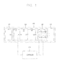
- FIG. 1 is a circuit diagram illustrating an inverter according to an embodiment of the present disclosure.
- the inverter 100 may include an input unit 110, a controller 115, a Cuk converter 120, a switching device unit 130, and an output unit 140.
- the input unit 110 output an input voltage (Vi) to the Cuk converter 120.
- the input unit 110 may include a capacitor (C1).
- An end of the capacitor (C1) within the input unit 110 is connected to a plus terminal, and the other end of the capacitor (C1) is connected to a minus terminal.
- the controller 115 controls the on/off of switches through a switching signal.
- the controller 115 adjusts the switching signal, thereby changing a switching duty of the switch.
- the Cuk converter 120 receives the input voltage (Vi) and outputs an output voltage (Vinv1) to the switching device unit 130.
- the Cuk converter 120 may include a first inductor (L1), a second inductor (L2), a first capacitor (C2), a second capacitor (C3), a diode (D1) and a switch (S5) within the converter.
- An end of the first inductor (L1) is connected to an end of the capacitor (C1), and the other end of the first inductor (L1) is connected to an end of the first capacitor (C2).
- An end of the switch (S5) within the converter is connected to a matching point between the first inductor (L1) and the first capacitor (C2), and the other end of the switch (S5) within the converter is connected to the minus terminal.
- the other end of the first capacitor (C2) is connected to an end of the second inductor (L2).
- the other end of the second inductor (L2) is connected to an end of the second capacitor (C3).
- the other end of the second capacitor (C3) is connected to the minus terminal.
- An anode of the diode (D1) is connected to a matching point between the first capacitor (C2) and the second inductor (L2), and a cathode of the diode (D1) is connected to the minus terminal.
- a ratio of the output voltage (Vinv1) of the Cuk converter 120 to the input voltage (Vi) may be defined as Equation 1.
- Vinv1/Vi D/(1-D) (Vinv1: output voltage of the Cuk converter 120, Vi: input voltage, D: switching duty of the switch (S5) within the Cuk converter)
- Equation 1 if the switching duty is changed, then the output voltage (Vinv1) of the Cuk converter 120 varies in correspondence to this.
- the controller 115 changes the switching duty (D) of the switch (S5) within the Cuk converter 120, then the output voltage (Vinv1) of the Cuk converter 120 varies in correspondence to the value of D. Accordingly, the output voltage (Vinv1) of the Cuk converter 120 with a user's desired form may be obtained by adjusting the value of D.
- the controller 115 adjusts the switching duty (D) of S5
- the Cuk converter 120 changes the input voltage (Vi) to a half-wave rectified sine waveform for the output.
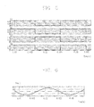
- FIG. 2 is a view illustrating the switching duty of a switch (S5) within the Cuk converter 120 according to an embodiment of the present disclosure
- FIG. 3 is a view illustrating the output voltage waveform of a Cuk converter according to an embodiment of the present disclosure.
- the Cuk converter 120 may output the output voltage of the Cuk converter 120 in the form of a half-wave rectified sine waveform voltage as illustrated in FIG. 3 .
- the switching device unit 130 receives the output voltage (Vinv1) of the Cuk converter 120 as an input and outputs the output voltage (Vout1).
- the switching device unit 130 may include four switches (S1, S2, S3, S4).
- the first and the second switch (S1, S2) and the third and the fourth switch (S3, S4) connected in series to each other are connected in parallel to the second capacitor (C3), respectively.
- the switches (S1-S4) operate by receiving a switching signal of the controller 115.
- the controller 115 may adjust the switching signal, thereby allowing a set of the first and the fourth switch (first switch set) and another set of the second and the third switch (second switch set) to be alternately switched for each set.
- the alternate timing of the switch is a time point at which the output voltage of the switching device unit 130 becomes zero.
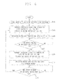
- FIG. 4 is a flow chart illustrating the output process of a switching device unit.
- the output process of the switching device unit 130 will be described with reference to FIG. 4 .
- the controller 115 senses the output voltage of the output voltage (Vinv1) of the Cuk converter 120 being received at the switching device unit 130.
- the output voltage (Vinv1) of the Cuk converter 120 has a half-wave rectified sine waveform (S101).
- the controller 115 transmits the switching signal to the switches (S1-S4) to turn off the first switch set (S1, S4) and turn on the second switch set (S2, S3) (S103).
- the switching device unit 130 When the first switch set (S1, S4) is turned off and the second switch set (S2, S3) is turned on, the switching device unit 130 outputs the input as it is. According to an embodiment of the present disclosure, the switching device unit 130 outputs a half-wave rectified sine waveform as it is (S105). In other words, a positive region of the sine waveform is output.
- the controller 115 transmits the switching signal to the switches (S1-S4) to turn off the second switch set and turn on the first switch set (S109). If the output of the switching device unit does not reach zero, then the controller 115 does not transmit the switching signal. Accordingly, the switching device unit 130 maintains a state of outputting the input as it is (S107).
- the switching device unit 130 When the controller 115 transmits the switching signal to the switches (S1-S4) to turn off the second switch set and turn on the first switch set, the switching device unit 130 outputs the input in a reverse manner (S111). In other words, the switching device unit 130 outputs a negative region of the sine wave.
- the controller 115 transmits the switching signal again to the switches (S1-S4) to turn off the first switch set (S1, S4) and turn on the second switch set (S2, S3). Then, the foregoing processes (S103-S113) are repeated again. If the output of the switching device unit 130 does not reach zero, then the controller 115 does not transmit the switching signal. Accordingly, the switching device unit 130 continues to output the reversed input (S113).
- the switching device unit 130 changes the input of a half-wave rectified sine waveform to a sine waveform for the output.
- the switching device unit 130 first, when the controller 115 turns on the second switch set and turns off the first switch set through the switching signal, the switching device unit 130 output a sine waveform for the output. Then, the switching device unit 130 outputs all the positive portion of the sine wave, the controller 115 turns off the second switch set and turn on the first switch set through the switching signal. At this time, the switching device unit 130 outputs the input in a reverse manner. In other words, the switching device unit 130 outputs a negative portion of the sine wave. Furthermore, the process may be repeated to form a sine waveform voltage.
- the positive direction of a sine waveform is output when switches S2, S3 within the switching device unit 130 are closed, and switches S1, S4 are open
- the negative direction of a sine waveform is output when switches S1, S4 within the switching device unit 130 are closed and switches S2, S3 are open.
- the controller 115 varies the duty of the switch (S5) in time such that a half-wave rectified sine waveform voltage is present at both ends of the diode, and controls the four switches (S1-S4) such that the output end outputs a sine waveform voltage.
- FIG. 5 is a view illustrating the switching duty of switches in a switching device unit according to an embodiment of the present disclosure.
- switches (S1-S4) in the switching device unit 130 are switched less frequently than the switch (S5) within the Cuk converter 120.
- the switches (S1, S2, S3, S4) within the switching device unit 130 merely performs the role of converting an output with a half-wave rectified sine waveform into a sine waveform, but the switches (S1, S2, S3, S4) within the switching device unit 130 does not involve in PWM control according to high-speed switching, thereby reducing switching loss compared to the related art.
- the output unit 140 outputs a value being output from the switching device unit 130.
- the switches (S1, S2, S3, S4) within the switching device unit 130 merely perform the role of converting an output with a half-wave rectified sine waveform into a sine waveform, but the switches (S1, S2, S3, S4) within the switching device unit 130 does not involve in PWM control according to high-speed switching, thereby reducing switching loss compared to the related art.
- the output unit 140 outputs a value (Vout1) being output from the switching device unit 130.
- the output unit 140 is output between the switch (S1) and switch (S2) and between the switch (S3) and switch (S4) among the switches within the switching device unit 130 as illustrated in FIG. 2 .
- FIG. 6 is a view illustrating the waveform of an output voltage according to an embodiment of the present disclosure.
- the output voltage (Vout1) As illustrated in FIG. 6 , the output voltage (Vout1) according to an embodiment of the present disclosure has a sine waveform.
- an inverter according to an embodiment of the present disclosure will be described with reference to FIGS. 7 through 11 .
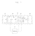
- FIG. 7 is view illustrating an inverter according to another embodiment of the present disclosure.
- an inverter 200 may include an input unit 110, a controller 115, a Cuk converter from which a filter portion is removed 220, a switching device unit 230, a filter unit 240, and an output unit 250.
- the Cuk converter from which a filter portion is removed 220 receives an input voltage (Vi) and outputs an output voltage (Vinv2) to the switching device unit 230.
- the Cuk converter from which a filter portion is removed 220 may include an inductor (L3), a capacitor (C4), a diode (D2) and a switch (S10) within the converter.
- L3 inductor
- C4 capacitor
- D2 diode
- S10 switch
- An end of the inductor (L3) is connected to an end of the capacitor (C1), and the other end of the inductor (L3) is connected to an end of the capacitor (C4).
- An end of the switch (S10) within the converter is connected to a matching point between the inductor (L1) and the capacitor (C4), and the other end of the switch (S10) within the converter is connected to the minus terminal.
- the other end of the capacitor (C4) is connected to an anode of the diode (D2).
- a cathode of the diode (D2) is connected to the minus terminal.
- a ratio of the output voltage (Vinv2) of the Cuk converter from which a filter portion is removed 220 to the input voltage (Vi) may be defined as Equation 2.
- Vinv2/Vi D/(1-D) (Vinv2: output voltage of the Cuk converter from which a filter portion is removed 220, Vi: input voltage, D: switching duty of the switch (S10) within the Cuk converter from which a filter portion is removed 220)
- Equation 2 if the switching duty is changed, then the output voltage (Vinv2) of the Cuk converter from which a filter portion is removed 220 varies in correspondence to this.
- the controller 115 changes the switching duty (D) of the switch (S10) within the Cuk converter from which a filter portion is removed 220, then the output voltage (Vinv2) of the Cuk converter from which a filter portion is removed 220 varies in correspondence to the value of D. Accordingly, the output voltage (Vinv2) of the Cuk converter from which a filter portion is removed 220 with a user's desired form may be obtained by adjusting the value of D.
- the Cuk converter from which a filter portion is removed 220 when the controller 115 adjusts the switching duty (D) of S10, the Cuk converter from which a filter portion is removed 220 according to an embodiment of the present disclosure changes the input voltage (Vi) to a half-wave rectified sine waveform PWM control voltage for the output.
- FIG. 8 is a view illustrating the switching duty of a switch within a Cuk converter from which a filter portion is removed according to an embodiment of the present disclosure
- FIG. 9 is a view illustrating the output voltage wave form diagram of a Cuk converter from which a filter portion is removed according to an embodiment of the present disclosure.
- the controller 115 when the controller 115 adjusts the switching duty of the switch (S10) within the Cuk converter from which a filter portion is removed 220 in an arbitrary manner as illustrated in FIG. 8 , the Cuk converter from which a filter portion is removed 220 may output the output (Vinv2) as a half-wave rectified sine waveform voltage as illustrated in FIG. 9 .
- the switching device unit 230 receives the output voltage (Vinv2) of the Cuk converter 220 as an input and outputs the output voltage (Vout2).
- the switching device unit 230 may include four switches (S6, S7, S8, S9).
- the first and the second switch (S6, S7) and the third and the fourth switch (S8, S9) connected in series to each other are connected in parallel to the diode (D2), respectively.
- the switches (S6-S9) operate by receiving a switching signal of the controller 115.
- the controller 115 may adjust the switching signal, thereby allowing a set of the sixth and the ninth switch (first switch set) and another set of the seventh and the eighth switch (second switch set) to be alternately switched for each set.
- the alternate timing of the switch is a time point at which the output voltage of the switching device unit 130 becomes zero.
- the output process of the switching device unit follows the foregoing processes (S103-S113).
- the switches S1-S4 correspond to the switches S6-S9, respectively.
- the input voltage of the switching device unit is a half-wave rectified sine waveform PWM control voltage other than a half-wave rectified sine waveform voltage.
- the controller 115 varies the duty of the switch (S10) in time such that a half-wave rectified sine waveform voltage is present at both ends of the diode, and controls the four switches (S6-S9) such that the output end outputs a sine waveform voltage.
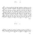
- FIG. 10 is a view illustrating the switching duty of switches in a switching device unit according to an embodiment of the present disclosure.
- switches (S6-S9) in the switching device unit 230 are switched less frequently than the switch (S10) within the Cuk converter from which a filter portion is removed 220.
- the switches (S6, S7, S8, S9) within the switching device unit 230 merely performs the role of converting a half-wave rectified sine waveform PWM control voltage into a sine waveform PWM control voltage, but the switches (S6, S7, S8, S9) within the switching device unit 230 does not involve in PWM control according to high-speed switching, thereby reducing switching loss compared to the related art.
- the filter unit 240 filters the output of the display unit 230.
- the filter unit 240 may include the inductor (L4) and the capacitor (C5).
- An end of the inductor (L4) is connected to a matching point between the switch (S6) and the switch (S7), and the other end of the inductor (L4) is connected to an end of the capacitor (C5).
- the other end of the capacitor (C5) is connected to a matching point between the switch (S8) and the switch (S9).
- the output unit 250 outputs a filtered value from the filter unit 240.
- the output unit 250 outputs a voltage (Vout2) at both ends of the capacitor (C5) as illustrated in FIG. 7 .
- FIG. 11 is a view illustrating the waveform of an output voltage according to an embodiment of the present disclosure.
- the output voltage (Vout2) has a sine waveform.
- the switching loss of the inverter may be reduced, thereby increasing the efficiency of the inverter.
- the foregoing embodiment according to the present disclosure may not be implemented only through an apparatus and a method using the same, and also implemented through a program for executing a function corresponding to the configuration of the embodiment according to the present disclosure or through a recording medium written with the program, and the implementation may be easily carried out by those skilled in the art to which the invention pertains from the foregoing description of the embodiment.
Landscapes
- Engineering & Computer Science (AREA)
- Power Engineering (AREA)
- Dc-Dc Converters (AREA)
- Inverter Devices (AREA)
Abstract
Description
- The present disclosure relates to an inverter, and more particularly, to an inverter with high efficiency.
- For an inverter in the related art, when an input voltage through the input unit is boosted or bucked through a DC/DC converter (boost converter or buck converter), the boosted or bucked voltage is switched at high speed using four switches through PWM control in the switching device unit to generate an AC voltage, which is subject to a filtering process with a filter and then subject to a process of converting the AC voltage into a DC voltage.
- However, according to the related art, all switched thereinside may be switched at high speed, thereby causing a problem in which a lot of switching loss is generated.
- A technical task of the present invention contrived to solve the foregoing problem is to reduce the number of switching cycles in a switch within the inverter, thereby reducing the switching loss of the inverter.
- In order to accomplish the foregoing objective, an inverter according to an embodiment of the present disclosure may include a converter having a switch, configured to convert a DC voltage into a half-wave rectified sine waveform voltage; a switching device unit having a switch, configured to convert the half-wave rectified sine waveform voltage into a sine waveform voltage; and a controller configured to control the on/off of the switch of the converter and the switch of the switching device unit.
- In order to accomplish the foregoing objective, an inverter according to an embodiment of the present disclosure may include a first inductor; a first switch having an end thereof connected to an end of the first inductor; a first capacitor having an end thereof connected to an end of the first switch; a diode having an anode connected to the other end of the first capacitor and a cathode connected to the other end of the first switch; four second switches connected in a bridge form having two input ends and two output ends; and a controller, wherein the two input ends are connected to both ends of the diode, respectively.
- The accompanying drawings, which are included to provide a further understanding of the invention and are incorporated in and constitute a part of this specification, illustrate embodiments of the invention and together with the description serve to explain the principles of the invention.
- In the drawings:
-
FIG. 1 is a circuit diagram illustrating an inverter according to an embodiment of the present disclosure; -
FIG. 2 is a view illustrating the switching duty of a switch within a converter according to an embodiment of the present disclosure; -
FIG. 3 is a view illustrating the output voltage waveform of a Cuk converter according to an embodiment of the present disclosure; -
FIG. 4 is a flow chart illustrating the output process of a switching device unit; -
FIG. 5 is a view illustrating the switching duty of switches in a switching device unit according to an embodiment of the present disclosure; -
FIG. 6 is a view illustrating the waveform of an output voltage according to an embodiment of the present disclosure; -
FIG. 7 is view illustrating an inverter according to another embodiment of the present disclosure; -
FIG. 8 is a view illustrating the switching duty of a switch within a Cuk converter from which a filter portion is removed according to an embodiment of the present disclosure; -
FIG. 9 is a view illustrating the output voltage wave form diagram of a Cuk converter from which a filter portion is removed according to an embodiment of the present disclosure; -
FIG. 10 is a view illustrating the switching duty of switches in a switching device unit according to an embodiment of the present disclosure; and -
FIG. 11 is a view illustrating the waveform of an output voltage according to an embodiment of the present disclosure. - Hereinafter, preferred embodiments of the present invention will be described in detail with reference to the accompanying drawings to such an extent that the present invention can be easily embodied by a person having ordinary skill in the art to which the present invention pertains. However, the present invention may be implemented in various different forms, and therefore, the present invention is not limited to the illustrated embodiments. In order to clearly describe the present invention, parts not related to the description are omitted, and like reference numerals designate like constituent elements throughout the specification.
- Throughout the specification, when a portion may "include" a certain constituent element, unless specified otherwise, it may not be construed to exclude another constituent element but may be construed to further include other constituent elements.
- Throughout the specification, in case where a portion is "connected" to the other portion, it may include a case of being electrically connected to the other portion by interposing another device therebetween as well as a case of being directly connected the other portion. An inverter according to the present disclosure may be operated as a single-phase inverter with a single device, a three-phase inverter when three devices are linked together, or the like.
- Furthermore, the inverter can be used in various applications, such as a grid connected type, a stand alone type, a motor drive type, for an apparatus in which the inverter is used.
- Hereinafter, an inverter according to an embodiment of the present disclosure will be described with reference to
FIGS. 1 through 6 . -
FIG. 1 is a circuit diagram illustrating an inverter according to an embodiment of the present disclosure. - As illustrated in
FIG. 1 , theinverter 100 according to an embodiment of the present disclosure may include aninput unit 110, acontroller 115, aCuk converter 120, aswitching device unit 130, and anoutput unit 140. - The
input unit 110 output an input voltage (Vi) to theCuk converter 120. Theinput unit 110 according to an embodiment of the present disclosure may include a capacitor (C1). - An end of the capacitor (C1) within the
input unit 110 according to an embodiment of the present disclosure is connected to a plus terminal, and the other end of the capacitor (C1) is connected to a minus terminal. - The
controller 115 controls the on/off of switches through a switching signal. - The
controller 115 according to an embodiment of the present disclosure adjusts the switching signal, thereby changing a switching duty of the switch. - The
Cuk converter 120 receives the input voltage (Vi) and outputs an output voltage (Vinv1) to theswitching device unit 130. - The
Cuk converter 120 according to an embodiment of the present disclosure may include a first inductor (L1), a second inductor (L2), a first capacitor (C2), a second capacitor (C3), a diode (D1) and a switch (S5) within the converter. - An end of the first inductor (L1) is connected to an end of the capacitor (C1), and the other end of the first inductor (L1) is connected to an end of the first capacitor (C2).
- An end of the switch (S5) within the converter is connected to a matching point between the first inductor (L1) and the first capacitor (C2), and the other end of the switch (S5) within the converter is connected to the minus terminal.
- The other end of the first capacitor (C2) is connected to an end of the second inductor (L2).
- The other end of the second inductor (L2) is connected to an end of the second capacitor (C3).
- The other end of the second capacitor (C3) is connected to the minus terminal.
- An anode of the diode (D1) is connected to a matching point between the first capacitor (C2) and the second inductor (L2), and a cathode of the diode (D1) is connected to the minus terminal.
- A ratio of the output voltage (Vinv1) of the
Cuk converter 120 to the input voltage (Vi) may be defined asEquation 1. - Vinv1/Vi = D/(1-D) (Vinv1: output voltage of the
Cuk converter 120, Vi: input voltage, D: switching duty of the switch (S5) within the Cuk converter) - According to
Equation 1, if the switching duty is changed, then the output voltage (Vinv1) of theCuk converter 120 varies in correspondence to this. - According to an embodiment of the present disclosure, in case where a constant DC voltage is applied to the input voltage (Vi), if the
controller 115 changes the switching duty (D) of the switch (S5) within theCuk converter 120, then the output voltage (Vinv1) of theCuk converter 120 varies in correspondence to the value of D. Accordingly, the output voltage (Vinv1) of theCuk converter 120 with a user's desired form may be obtained by adjusting the value of D. According to an embodiment of the present disclosure, when thecontroller 115 adjusts the switching duty (D) of S5, theCuk converter 120 according to an embodiment of the present disclosure changes the input voltage (Vi) to a half-wave rectified sine waveform for the output. -
FIG. 2 is a view illustrating the switching duty of a switch (S5) within theCuk converter 120 according to an embodiment of the present disclosure, andFIG. 3 is a view illustrating the output voltage waveform of a Cuk converter according to an embodiment of the present disclosure. - According to an embodiment of the present disclosure, when the
controller 115 adjusts the switching duty of the switch (S5) within theconverter 120 in an arbitrary manner as illustrated inFIG. 2 , theCuk converter 120 may output the output voltage of theCuk converter 120 in the form of a half-wave rectified sine waveform voltage as illustrated inFIG. 3 . - The
switching device unit 130 receives the output voltage (Vinv1) of theCuk converter 120 as an input and outputs the output voltage (Vout1). - The
switching device unit 130 according to an embodiment of the present disclosure may include four switches (S1, S2, S3, S4). - For the switches according to an embodiment of the present disclosure, the first and the second switch (S1, S2) and the third and the fourth switch (S3, S4) connected in series to each other are connected in parallel to the second capacitor (C3), respectively.
- The switches (S1-S4) according to an embodiment of the present disclosure operate by receiving a switching signal of the
controller 115. According to an embodiment of the present disclosure, thecontroller 115 may adjust the switching signal, thereby allowing a set of the first and the fourth switch (first switch set) and another set of the second and the third switch (second switch set) to be alternately switched for each set. - The alternate timing of the switch is a time point at which the output voltage of the
switching device unit 130 becomes zero. -
FIG. 4 is a flow chart illustrating the output process of a switching device unit. - The output process of the
switching device unit 130 will be described with reference toFIG. 4 . - The
controller 115 senses the output voltage of the output voltage (Vinv1) of theCuk converter 120 being received at theswitching device unit 130. According to an embodiment of the present disclosure, the output voltage (Vinv1) of theCuk converter 120 has a half-wave rectified sine waveform (S101). - Then, the
controller 115 transmits the switching signal to the switches (S1-S4) to turn off the first switch set (S1, S4) and turn on the second switch set (S2, S3) (S103). - When the first switch set (S1, S4) is turned off and the second switch set (S2, S3) is turned on, the
switching device unit 130 outputs the input as it is. According to an embodiment of the present disclosure, theswitching device unit 130 outputs a half-wave rectified sine waveform as it is (S105). In other words, a positive region of the sine waveform is output. - Then, when the output of the
switching device unit 130 reaches zero, thecontroller 115 transmits the switching signal to the switches (S1-S4) to turn off the second switch set and turn on the first switch set (S109). If the output of the switching device unit does not reach zero, then thecontroller 115 does not transmit the switching signal. Accordingly, theswitching device unit 130 maintains a state of outputting the input as it is (S107). - When the
controller 115 transmits the switching signal to the switches (S1-S4) to turn off the second switch set and turn on the first switch set, theswitching device unit 130 outputs the input in a reverse manner (S111). In other words, theswitching device unit 130 outputs a negative region of the sine wave. - Then, the output of the
switching device unit 130 reaches zero again, thecontroller 115 transmits the switching signal again to the switches (S1-S4) to turn off the first switch set (S1, S4) and turn on the second switch set (S2, S3). Then, the foregoing processes (S103-S113) are repeated again. If the output of theswitching device unit 130 does not reach zero, then thecontroller 115 does not transmit the switching signal. Accordingly, theswitching device unit 130 continues to output the reversed input (S113). - According to an embodiment of the present disclosure, through the processes (S101-S113), the
switching device unit 130 changes the input of a half-wave rectified sine waveform to a sine waveform for the output. - According to an embodiment of the present disclosure, first, when the
controller 115 turns on the second switch set and turns off the first switch set through the switching signal, theswitching device unit 130 output a sine waveform for the output. Then, theswitching device unit 130 outputs all the positive portion of the sine wave, thecontroller 115 turns off the second switch set and turn on the first switch set through the switching signal. At this time, theswitching device unit 130 outputs the input in a reverse manner. In other words, theswitching device unit 130 outputs a negative portion of the sine wave. Furthermore, the process may be repeated to form a sine waveform voltage. - Accordingly, the positive direction of a sine waveform is output when switches S2, S3 within the
switching device unit 130 are closed, and switches S1, S4 are open, and the negative direction of a sine waveform is output when switches S1, S4 within theswitching device unit 130 are closed and switches S2, S3 are open. - According to an embodiment of the present disclosure, the
controller 115 varies the duty of the switch (S5) in time such that a half-wave rectified sine waveform voltage is present at both ends of the diode, and controls the four switches (S1-S4) such that the output end outputs a sine waveform voltage. -
FIG. 5 is a view illustrating the switching duty of switches in a switching device unit according to an embodiment of the present disclosure. - Referring to
FIG. 5 , it is seen that the switches (S1-S4) in theswitching device unit 130 are switched less frequently than the switch (S5) within theCuk converter 120. - In this manner, contrary to the related art, the switches (S1, S2, S3, S4) within the
switching device unit 130 merely performs the role of converting an output with a half-wave rectified sine waveform into a sine waveform, but the switches (S1, S2, S3, S4) within theswitching device unit 130 does not involve in PWM control according to high-speed switching, thereby reducing switching loss compared to the related art. - The
output unit 140 outputs a value being output from theswitching device unit 130. - Owing to such a method, the switches (S1, S2, S3, S4) within the
switching device unit 130 merely perform the role of converting an output with a half-wave rectified sine waveform into a sine waveform, but the switches (S1, S2, S3, S4) within theswitching device unit 130 does not involve in PWM control according to high-speed switching, thereby reducing switching loss compared to the related art. - The
output unit 140 outputs a value (Vout1) being output from theswitching device unit 130. - The
output unit 140 according to an embodiment of the present disclosure is output between the switch (S1) and switch (S2) and between the switch (S3) and switch (S4) among the switches within theswitching device unit 130 as illustrated inFIG. 2 . -
FIG. 6 is a view illustrating the waveform of an output voltage according to an embodiment of the present disclosure. - As illustrated in
FIG. 6 , the output voltage (Vout1) according to an embodiment of the present disclosure has a sine waveform. Next, an inverter according to an embodiment of the present disclosure will be described with reference toFIGS. 7 through 11 . -
FIG. 7 is view illustrating an inverter according to another embodiment of the present disclosure. - As illustrated in
FIG. 7 , aninverter 200 according to an embodiment of the present disclosure may include aninput unit 110, acontroller 115, a Cuk converter from which a filter portion is removed 220, a switching device unit 230, a filter unit 240, and an output unit 250. - The Cuk converter from which a filter portion is removed 220 receives an input voltage (Vi) and outputs an output voltage (Vinv2) to the switching device unit 230.
- The Cuk converter from which a filter portion is removed 220 according to an embodiment of the present disclosure may include an inductor (L3), a capacitor (C4), a diode (D2) and a switch (S10) within the converter.
- An end of the inductor (L3) is connected to an end of the capacitor (C1), and the other end of the inductor (L3) is connected to an end of the capacitor (C4).
- An end of the switch (S10) within the converter is connected to a matching point between the inductor (L1) and the capacitor (C4), and the other end of the switch (S10) within the converter is connected to the minus terminal.
- The other end of the capacitor (C4) is connected to an anode of the diode (D2).
- A cathode of the diode (D2) is connected to the minus terminal.
- A ratio of the output voltage (Vinv2) of the Cuk converter from which a filter portion is removed 220 to the input voltage (Vi) may be defined as
Equation 2. - Vinv2/Vi = D/(1-D) (Vinv2: output voltage of the Cuk converter from which a filter portion is removed 220, Vi: input voltage, D: switching duty of the switch (S10) within the Cuk converter from which a filter portion is removed 220)
- According to
Equation 2, if the switching duty is changed, then the output voltage (Vinv2) of the Cuk converter from which a filter portion is removed 220 varies in correspondence to this. - According to an embodiment of the present disclosure, in case where a constant DC voltage is applied to the input voltage (Vi), if the
controller 115 changes the switching duty (D) of the switch (S10) within the Cuk converter from which a filter portion is removed 220, then the output voltage (Vinv2) of the Cuk converter from which a filter portion is removed 220 varies in correspondence to the value of D. Accordingly, the output voltage (Vinv2) of the Cuk converter from which a filter portion is removed 220 with a user's desired form may be obtained by adjusting the value of D. According to an embodiment of the present disclosure, when thecontroller 115 adjusts the switching duty (D) of S10, the Cuk converter from which a filter portion is removed 220 according to an embodiment of the present disclosure changes the input voltage (Vi) to a half-wave rectified sine waveform PWM control voltage for the output. -
FIG. 8 is a view illustrating the switching duty of a switch within a Cuk converter from which a filter portion is removed according to an embodiment of the present disclosure, andFIG. 9 is a view illustrating the output voltage wave form diagram of a Cuk converter from which a filter portion is removed according to an embodiment of the present disclosure. - According to an embodiment of the present disclosure, when the
controller 115 adjusts the switching duty of the switch (S10) within the Cuk converter from which a filter portion is removed 220 in an arbitrary manner as illustrated inFIG. 8 , the Cuk converter from which a filter portion is removed 220 may output the output (Vinv2) as a half-wave rectified sine waveform voltage as illustrated inFIG. 9 . - The switching device unit 230 receives the output voltage (Vinv2) of the Cuk converter 220 as an input and outputs the output voltage (Vout2).
- The switching device unit 230 according to an embodiment of the present disclosure may include four switches (S6, S7, S8, S9).
- For the switches according to an embodiment of the present disclosure, the first and the second switch (S6, S7) and the third and the fourth switch (S8, S9) connected in series to each other are connected in parallel to the diode (D2), respectively.
- The switches (S6-S9) according to an embodiment of the present disclosure operate by receiving a switching signal of the
controller 115. According to an embodiment of the present disclosure, thecontroller 115 may adjust the switching signal, thereby allowing a set of the sixth and the ninth switch (first switch set) and another set of the seventh and the eighth switch (second switch set) to be alternately switched for each set. - The alternate timing of the switch is a time point at which the output voltage of the
switching device unit 130 becomes zero. - The output process of the switching device unit follows the foregoing processes (S103-S113). However, the switches S1-S4 correspond to the switches S6-S9, respectively. Furthermore, the input voltage of the switching device unit is a half-wave rectified sine waveform PWM control voltage other than a half-wave rectified sine waveform voltage.
- According to an embodiment of the present disclosure, the
controller 115 varies the duty of the switch (S10) in time such that a half-wave rectified sine waveform voltage is present at both ends of the diode, and controls the four switches (S6-S9) such that the output end outputs a sine waveform voltage. -
FIG. 10 is a view illustrating the switching duty of switches in a switching device unit according to an embodiment of the present disclosure. - Referring to
FIG. 10 , it is seen that the switches (S6-S9) in the switching device unit 230 are switched less frequently than the switch (S10) within the Cuk converter from which a filter portion is removed 220. - In this manner, contrary to the related art, the switches (S6, S7, S8, S9) within the switching device unit 230 merely performs the role of converting a half-wave rectified sine waveform PWM control voltage into a sine waveform PWM control voltage, but the switches (S6, S7, S8, S9) within the switching device unit 230 does not involve in PWM control according to high-speed switching, thereby reducing switching loss compared to the related art.
- The filter unit 240 filters the output of the display unit 230.
- The filter unit 240 may include the inductor (L4) and the capacitor (C5).
- An end of the inductor (L4) is connected to a matching point between the switch (S6) and the switch (S7), and the other end of the inductor (L4) is connected to an end of the capacitor (C5).
- The other end of the capacitor (C5) is connected to a matching point between the switch (S8) and the switch (S9).
- The output unit 250 outputs a filtered value from the filter unit 240.
- The output unit 250 according to an embodiment of the present disclosure outputs a voltage (Vout2) at both ends of the capacitor (C5) as illustrated in
FIG. 7 . -
FIG. 11 is a view illustrating the waveform of an output voltage according to an embodiment of the present disclosure. - As illustrated in
FIG. 11 , the output voltage (Vout2) according to an embodiment of the present disclosure has a sine waveform. - According to an embodiment of the present disclosure, the switching loss of the inverter may be reduced, thereby increasing the efficiency of the inverter.
- The foregoing embodiment according to the present disclosure may not be implemented only through an apparatus and a method using the same, and also implemented through a program for executing a function corresponding to the configuration of the embodiment according to the present disclosure or through a recording medium written with the program, and the implementation may be easily carried out by those skilled in the art to which the invention pertains from the foregoing description of the embodiment.
- Although the embodiment of the present disclosure has been described in detail, the rights scope of the present invention is not limited to the embodiments and various modifications and improvements thereto made by those skilled in the art using the basic concept of the present invention as defined in the accompanying claims will fall in the rights scope of the invention.
Claims (9)
- An inverter (100) for converting DC voltage to AC voltage, the inverter (100), comprising:a converter (120) having a switch, configured to convert the DC voltage into a half-wave rectified sine waveform voltage;a switching device (130) unit having a switch, configured to convert the half-wave rectified sine waveform voltage into a sine waveform voltage; anda controller (115) configured to control the on/off of the switch of the converter (120) and the switch of the switching device (130) unit.
- The inverter (100) of claim 1, wherein the converter (120) is a Cuk converter.
- The inverter (100) of any of claims 1 to 2, wherein the converter (120) comprises a filter.
- The inverter (100) of any of claims 1 to 2, wherein a filter is located at an output end of the switching device (130) unit.
- The inverter (100) of any of claims 1 to 4, wherein the controller (115) varies the switching duty of a switch within the Cuk converter in time such that a half-wave rectified sine waveform voltage is present at an output end of the Cuk converter, and controls the switch of the switching device (130) unit such that a sine waveform voltage is output at an output end of the inverter (100).
- An inverter (200) for converting DC voltage to AC voltage, the inverter (200), comprising:a first inductor (L3);a first switch (S10) having an end thereof connected to an end of the first inductor (L3);a first capacitor (C4) having an end thereof connected to an end of the first switch (S10);a diode (D2) having an anode connected to the other end of the first capacitor (C4) and a cathode connected to the other end of the first switch (S10);four second switches (230) connected in a bridge form having two input ends and two output ends; anda controller (115),wherein the two input ends are connected to both ends of the diode (D2), respectively.
- The inverter (200) of claim 6, wherein the controller (115) varies the duty of the first switch (S10) in time such that a half-wave rectified sine waveform voltage is present at both ends of the diode (D2), and controls the four second switches (230) such that the two output ends output sine waveform voltages.
- The inverter (200) of claim 7, further comprising:an inductor connected to an anode of the diode (D2); anda capacitor connected to the other end of the inverter (200) and a cathode of the diode (D2).
- The inverter (200) of any of claims 7 to 8, further comprising:an inductor an end of which is connected to either one of the two output ends; anda capacitor an end of which is connected to the other one of the two output ends,wherein the other end of the inductor and the other end of the capacitor are connected to each other.
Applications Claiming Priority (1)
| Application Number | Priority Date | Filing Date | Title |
|---|---|---|---|
| KR1020120098501A KR20140031766A (en) | 2012-09-05 | 2012-09-05 | Inverter and driving method thereof |
Publications (2)
| Publication Number | Publication Date |
|---|---|
| EP2706655A1 true EP2706655A1 (en) | 2014-03-12 |
| EP2706655B1 EP2706655B1 (en) | 2016-08-24 |
Family
ID=49084893
Family Applications (1)
| Application Number | Title | Priority Date | Filing Date |
|---|---|---|---|
| EP13182973.1A Not-in-force EP2706655B1 (en) | 2012-09-05 | 2013-09-04 | Inverter |
Country Status (6)
| Country | Link |
|---|---|
| US (1) | US8971078B2 (en) |
| EP (1) | EP2706655B1 (en) |
| JP (1) | JP2014054175A (en) |
| KR (1) | KR20140031766A (en) |
| CN (1) | CN103684006A (en) |
| ES (1) | ES2602265T3 (en) |
Cited By (1)
| Publication number | Priority date | Publication date | Assignee | Title |
|---|---|---|---|---|
| WO2016050477A1 (en) * | 2014-09-30 | 2016-04-07 | Siemens Aktiengesellschaft | Device and method for generating an alternating voltage using a step-down converter with a pole-reversing bridge |
Families Citing this family (1)
| Publication number | Priority date | Publication date | Assignee | Title |
|---|---|---|---|---|
| KR102589640B1 (en) * | 2018-12-12 | 2023-10-16 | 삼성전자주식회사 | Converter and circuit device including the same |
Citations (2)
| Publication number | Priority date | Publication date | Assignee | Title |
|---|---|---|---|---|
| WO2011029650A1 (en) * | 2009-09-11 | 2011-03-17 | Robert Bosch Gmbh | Dc-ac inverter assembly, in particular solar cell inverter |
| DE102011017601A1 (en) * | 2011-04-27 | 2012-10-31 | Robert Bosch Gmbh | Control method for an inverter and inverter arrangement, in particular solar cell inverter |
Family Cites Families (7)
| Publication number | Priority date | Publication date | Assignee | Title |
|---|---|---|---|---|
| FR2508737B1 (en) * | 1981-06-24 | 1986-03-21 | Westinghouse Electric Corp | APPARATUS FOR CONTROLLING AC MOTORS |
| JP3245523B2 (en) * | 1995-10-16 | 2002-01-15 | シャープ株式会社 | Inverter control method and inverter control device |
| JPH09252593A (en) * | 1996-03-14 | 1997-09-22 | Sharp Corp | Inverter device |
| US5969484A (en) * | 1998-05-14 | 1999-10-19 | Optimum Power Conversion, Inc. | Electronic ballast |
| EP1249928A1 (en) | 2001-04-10 | 2002-10-16 | Siemens Aktiengesellschaft | Method and voltage-converter for transforming an input DC voltage into an AC voltage with a frequency close to the grid frequency |
| TWI332742B (en) * | 2006-04-21 | 2010-11-01 | Delta Electronics Inc | Uninterruptible power supply capable of providing sinusoidal-wave ouput ac voltage and method thereof |
| TWI455470B (en) * | 2011-12-30 | 2014-10-01 | Nat Univ Tsing Hua | Two - stage isolated DC / AC conversion circuit architecture |
-
2012
- 2012-09-05 KR KR1020120098501A patent/KR20140031766A/en not_active Ceased
-
2013
- 2013-09-04 EP EP13182973.1A patent/EP2706655B1/en not_active Not-in-force
- 2013-09-04 JP JP2013183364A patent/JP2014054175A/en active Pending
- 2013-09-04 US US14/017,873 patent/US8971078B2/en active Active
- 2013-09-04 ES ES13182973.1T patent/ES2602265T3/en active Active
- 2013-09-05 CN CN201310485922.1A patent/CN103684006A/en active Pending
Patent Citations (2)
| Publication number | Priority date | Publication date | Assignee | Title |
|---|---|---|---|---|
| WO2011029650A1 (en) * | 2009-09-11 | 2011-03-17 | Robert Bosch Gmbh | Dc-ac inverter assembly, in particular solar cell inverter |
| DE102011017601A1 (en) * | 2011-04-27 | 2012-10-31 | Robert Bosch Gmbh | Control method for an inverter and inverter arrangement, in particular solar cell inverter |
Non-Patent Citations (1)
| Title |
|---|
| SANCHIS P ET AL: "Operation and control of a high performance inverter consisting of a buck-boost and a zero switching losses H-bridge for photovoltaic systems", POWER ELECTRONICS SPECIALISTS CONFERENCE, 2004. PESC 04. 2004 IEEE 35TH ANNUAL, AACHEN, GERMANY 20-25 JUNE 2004, PISCATAWAY, NJ, USA,IEEE, US, vol. 3, 20 June 2004 (2004-06-20), pages 2089 - 2094, XP010739593, ISBN: 978-0-7803-8399-9, DOI: 10.1109/PESC.2004.1355440 * |
Cited By (1)
| Publication number | Priority date | Publication date | Assignee | Title |
|---|---|---|---|---|
| WO2016050477A1 (en) * | 2014-09-30 | 2016-04-07 | Siemens Aktiengesellschaft | Device and method for generating an alternating voltage using a step-down converter with a pole-reversing bridge |
Also Published As
| Publication number | Publication date |
|---|---|
| KR20140031766A (en) | 2014-03-13 |
| JP2014054175A (en) | 2014-03-20 |
| US8971078B2 (en) | 2015-03-03 |
| EP2706655B1 (en) | 2016-08-24 |
| ES2602265T3 (en) | 2017-02-20 |
| CN103684006A (en) | 2014-03-26 |
| US20140063881A1 (en) | 2014-03-06 |
Similar Documents
| Publication | Publication Date | Title |
|---|---|---|
| US10958180B2 (en) | DC-DC converter for wide input voltage | |
| US9263967B2 (en) | AC/DC power conversion methods and apparatus | |
| US8811048B2 (en) | Medium voltage variable frequency driving system | |
| EP3317955A1 (en) | Electric power conversion apparatus | |
| TW200939602A (en) | Parallel-connected resonant converter circuit and controlling method thereof | |
| JP2007110856A (en) | Bidirectional dc-ac inverter | |
| CN101588139A (en) | High power factor isolated buck-type power factor correction converter | |
| KR101681958B1 (en) | Cascaded multilevel ac-ac converter | |
| JP2014197945A (en) | Power conversion device and motor drive device having the same | |
| WO2015141319A1 (en) | Power conditioner and method for controlling same | |
| EP2317637B1 (en) | Circuit device for driving an AC electric load | |
| EP2706655B1 (en) | Inverter | |
| CN104410278B (en) | DCDC converter | |
| JP2008086107A (en) | Motor drive control device | |
| CN218276471U (en) | A two-wire PFC circuit and device | |
| KR101300273B1 (en) | Apparatus for controlling operation of air conditioner | |
| CN100367646C (en) | Single/Three-phase Impedance Source Up/Down Voltage AC/AC Converter | |
| JP2017112686A (en) | AC power supply circuit | |
| JP5340130B2 (en) | DC / DC power converter | |
| KR100900940B1 (en) | Emergency drive device for three-phase induction motor | |
| CN113890384A (en) | A single-phase Cuk variable frequency AC-AC converter | |
| CN114552993B (en) | A dual-wire PFC circuit and device | |
| KR20150066379A (en) | Synchronous rectifier circuit of three-phase step down resonant type | |
| US20250128620A1 (en) | Transformerless bidirectional dc charger for electric vehicles | |
| JP2015080370A (en) | Power conversion device |
Legal Events
| Date | Code | Title | Description |
|---|---|---|---|
| PUAI | Public reference made under article 153(3) epc to a published international application that has entered the european phase |
Free format text: ORIGINAL CODE: 0009012 |
|
| AK | Designated contracting states |
Kind code of ref document: A1 Designated state(s): AL AT BE BG CH CY CZ DE DK EE ES FI FR GB GR HR HU IE IS IT LI LT LU LV MC MK MT NL NO PL PT RO RS SE SI SK SM TR |
|
| AX | Request for extension of the european patent |
Extension state: BA ME |
|
| 17P | Request for examination filed |
Effective date: 20140331 |
|
| RBV | Designated contracting states (corrected) |
Designated state(s): AL AT BE BG CH CY CZ DE DK EE ES FI FR GB GR HR HU IE IS IT LI LT LU LV MC MK MT NL NO PL PT RO RS SE SI SK SM TR |
|
| 17Q | First examination report despatched |
Effective date: 20150303 |
|
| GRAP | Despatch of communication of intention to grant a patent |
Free format text: ORIGINAL CODE: EPIDOSNIGR1 |
|
| INTG | Intention to grant announced |
Effective date: 20160331 |
|
| GRAS | Grant fee paid |
Free format text: ORIGINAL CODE: EPIDOSNIGR3 |
|
| GRAA | (expected) grant |
Free format text: ORIGINAL CODE: 0009210 |
|
| AK | Designated contracting states |
Kind code of ref document: B1 Designated state(s): AL AT BE BG CH CY CZ DE DK EE ES FI FR GB GR HR HU IE IS IT LI LT LU LV MC MK MT NL NO PL PT RO RS SE SI SK SM TR |
|
| REG | Reference to a national code |
Ref country code: GB Ref legal event code: FG4D |
|
| REG | Reference to a national code |
Ref country code: CH Ref legal event code: EP |
|
| REG | Reference to a national code |
Ref country code: AT Ref legal event code: REF Ref document number: 823858 Country of ref document: AT Kind code of ref document: T Effective date: 20160915 |
|
| REG | Reference to a national code |
Ref country code: IE Ref legal event code: FG4D |
|
| REG | Reference to a national code |
Ref country code: FR Ref legal event code: PLFP Year of fee payment: 4 |
|
| REG | Reference to a national code |
Ref country code: DE Ref legal event code: R096 Ref document number: 602013010547 Country of ref document: DE |
|
| REG | Reference to a national code |
Ref country code: LT Ref legal event code: MG4D |
|
| REG | Reference to a national code |
Ref country code: NL Ref legal event code: MP Effective date: 20160824 |
|
| REG | Reference to a national code |
Ref country code: AT Ref legal event code: MK05 Ref document number: 823858 Country of ref document: AT Kind code of ref document: T Effective date: 20160824 |
|
| PG25 | Lapsed in a contracting state [announced via postgrant information from national office to epo] |
Ref country code: HR Free format text: LAPSE BECAUSE OF FAILURE TO SUBMIT A TRANSLATION OF THE DESCRIPTION OR TO PAY THE FEE WITHIN THE PRESCRIBED TIME-LIMIT Effective date: 20160824 Ref country code: RS Free format text: LAPSE BECAUSE OF FAILURE TO SUBMIT A TRANSLATION OF THE DESCRIPTION OR TO PAY THE FEE WITHIN THE PRESCRIBED TIME-LIMIT Effective date: 20160824 Ref country code: NL Free format text: LAPSE BECAUSE OF FAILURE TO SUBMIT A TRANSLATION OF THE DESCRIPTION OR TO PAY THE FEE WITHIN THE PRESCRIBED TIME-LIMIT Effective date: 20160824 Ref country code: FI Free format text: LAPSE BECAUSE OF FAILURE TO SUBMIT A TRANSLATION OF THE DESCRIPTION OR TO PAY THE FEE WITHIN THE PRESCRIBED TIME-LIMIT Effective date: 20160824 Ref country code: NO Free format text: LAPSE BECAUSE OF FAILURE TO SUBMIT A TRANSLATION OF THE DESCRIPTION OR TO PAY THE FEE WITHIN THE PRESCRIBED TIME-LIMIT Effective date: 20161124 Ref country code: LT Free format text: LAPSE BECAUSE OF FAILURE TO SUBMIT A TRANSLATION OF THE DESCRIPTION OR TO PAY THE FEE WITHIN THE PRESCRIBED TIME-LIMIT Effective date: 20160824 |
|
| REG | Reference to a national code |
Ref country code: ES Ref legal event code: FG2A Ref document number: 2602265 Country of ref document: ES Kind code of ref document: T3 Effective date: 20170220 |
|
| PG25 | Lapsed in a contracting state [announced via postgrant information from national office to epo] |
Ref country code: BE Free format text: LAPSE BECAUSE OF NON-PAYMENT OF DUE FEES Effective date: 20160930 Ref country code: SE Free format text: LAPSE BECAUSE OF FAILURE TO SUBMIT A TRANSLATION OF THE DESCRIPTION OR TO PAY THE FEE WITHIN THE PRESCRIBED TIME-LIMIT Effective date: 20160824 Ref country code: GR Free format text: LAPSE BECAUSE OF FAILURE TO SUBMIT A TRANSLATION OF THE DESCRIPTION OR TO PAY THE FEE WITHIN THE PRESCRIBED TIME-LIMIT Effective date: 20161125 Ref country code: LV Free format text: LAPSE BECAUSE OF FAILURE TO SUBMIT A TRANSLATION OF THE DESCRIPTION OR TO PAY THE FEE WITHIN THE PRESCRIBED TIME-LIMIT Effective date: 20160824 Ref country code: AT Free format text: LAPSE BECAUSE OF FAILURE TO SUBMIT A TRANSLATION OF THE DESCRIPTION OR TO PAY THE FEE WITHIN THE PRESCRIBED TIME-LIMIT Effective date: 20160824 Ref country code: PT Free format text: LAPSE BECAUSE OF FAILURE TO SUBMIT A TRANSLATION OF THE DESCRIPTION OR TO PAY THE FEE WITHIN THE PRESCRIBED TIME-LIMIT Effective date: 20161226 |
|
| PG25 | Lapsed in a contracting state [announced via postgrant information from national office to epo] |
Ref country code: RO Free format text: LAPSE BECAUSE OF FAILURE TO SUBMIT A TRANSLATION OF THE DESCRIPTION OR TO PAY THE FEE WITHIN THE PRESCRIBED TIME-LIMIT Effective date: 20160824 Ref country code: EE Free format text: LAPSE BECAUSE OF FAILURE TO SUBMIT A TRANSLATION OF THE DESCRIPTION OR TO PAY THE FEE WITHIN THE PRESCRIBED TIME-LIMIT Effective date: 20160824 |
|
| REG | Reference to a national code |
Ref country code: CH Ref legal event code: PL |
|
| REG | Reference to a national code |
Ref country code: DE Ref legal event code: R097 Ref document number: 602013010547 Country of ref document: DE |
|
| PG25 | Lapsed in a contracting state [announced via postgrant information from national office to epo] |
Ref country code: SM Free format text: LAPSE BECAUSE OF FAILURE TO SUBMIT A TRANSLATION OF THE DESCRIPTION OR TO PAY THE FEE WITHIN THE PRESCRIBED TIME-LIMIT Effective date: 20160824 Ref country code: PL Free format text: LAPSE BECAUSE OF FAILURE TO SUBMIT A TRANSLATION OF THE DESCRIPTION OR TO PAY THE FEE WITHIN THE PRESCRIBED TIME-LIMIT Effective date: 20160824 Ref country code: CZ Free format text: LAPSE BECAUSE OF FAILURE TO SUBMIT A TRANSLATION OF THE DESCRIPTION OR TO PAY THE FEE WITHIN THE PRESCRIBED TIME-LIMIT Effective date: 20160824 Ref country code: BG Free format text: LAPSE BECAUSE OF FAILURE TO SUBMIT A TRANSLATION OF THE DESCRIPTION OR TO PAY THE FEE WITHIN THE PRESCRIBED TIME-LIMIT Effective date: 20161124 Ref country code: SK Free format text: LAPSE BECAUSE OF FAILURE TO SUBMIT A TRANSLATION OF THE DESCRIPTION OR TO PAY THE FEE WITHIN THE PRESCRIBED TIME-LIMIT Effective date: 20160824 Ref country code: DK Free format text: LAPSE BECAUSE OF FAILURE TO SUBMIT A TRANSLATION OF THE DESCRIPTION OR TO PAY THE FEE WITHIN THE PRESCRIBED TIME-LIMIT Effective date: 20160824 Ref country code: BE Free format text: LAPSE BECAUSE OF FAILURE TO SUBMIT A TRANSLATION OF THE DESCRIPTION OR TO PAY THE FEE WITHIN THE PRESCRIBED TIME-LIMIT Effective date: 20160824 |
|
| REG | Reference to a national code |
Ref country code: FR Ref legal event code: PLFP Year of fee payment: 5 |
|
| REG | Reference to a national code |
Ref country code: IE Ref legal event code: MM4A |
|
| PG25 | Lapsed in a contracting state [announced via postgrant information from national office to epo] |
Ref country code: MC Free format text: LAPSE BECAUSE OF FAILURE TO SUBMIT A TRANSLATION OF THE DESCRIPTION OR TO PAY THE FEE WITHIN THE PRESCRIBED TIME-LIMIT Effective date: 20160824 |
|
| PLBE | No opposition filed within time limit |
Free format text: ORIGINAL CODE: 0009261 |
|
| STAA | Information on the status of an ep patent application or granted ep patent |
Free format text: STATUS: NO OPPOSITION FILED WITHIN TIME LIMIT |
|
| PG25 | Lapsed in a contracting state [announced via postgrant information from national office to epo] |
Ref country code: LI Free format text: LAPSE BECAUSE OF NON-PAYMENT OF DUE FEES Effective date: 20160930 Ref country code: IE Free format text: LAPSE BECAUSE OF NON-PAYMENT OF DUE FEES Effective date: 20160904 Ref country code: CH Free format text: LAPSE BECAUSE OF NON-PAYMENT OF DUE FEES Effective date: 20160930 |
|
| 26N | No opposition filed |
Effective date: 20170526 |
|
| PG25 | Lapsed in a contracting state [announced via postgrant information from national office to epo] |
Ref country code: SI Free format text: LAPSE BECAUSE OF FAILURE TO SUBMIT A TRANSLATION OF THE DESCRIPTION OR TO PAY THE FEE WITHIN THE PRESCRIBED TIME-LIMIT Effective date: 20160824 Ref country code: LU Free format text: LAPSE BECAUSE OF NON-PAYMENT OF DUE FEES Effective date: 20160904 |
|
| PG25 | Lapsed in a contracting state [announced via postgrant information from national office to epo] |
Ref country code: HU Free format text: LAPSE BECAUSE OF FAILURE TO SUBMIT A TRANSLATION OF THE DESCRIPTION OR TO PAY THE FEE WITHIN THE PRESCRIBED TIME-LIMIT; INVALID AB INITIO Effective date: 20130904 Ref country code: CY Free format text: LAPSE BECAUSE OF FAILURE TO SUBMIT A TRANSLATION OF THE DESCRIPTION OR TO PAY THE FEE WITHIN THE PRESCRIBED TIME-LIMIT Effective date: 20160824 |
|
| REG | Reference to a national code |
Ref country code: FR Ref legal event code: PLFP Year of fee payment: 6 |
|
| PG25 | Lapsed in a contracting state [announced via postgrant information from national office to epo] |
Ref country code: MK Free format text: LAPSE BECAUSE OF FAILURE TO SUBMIT A TRANSLATION OF THE DESCRIPTION OR TO PAY THE FEE WITHIN THE PRESCRIBED TIME-LIMIT Effective date: 20160824 Ref country code: IS Free format text: LAPSE BECAUSE OF FAILURE TO SUBMIT A TRANSLATION OF THE DESCRIPTION OR TO PAY THE FEE WITHIN THE PRESCRIBED TIME-LIMIT Effective date: 20160824 Ref country code: MT Free format text: LAPSE BECAUSE OF NON-PAYMENT OF DUE FEES Effective date: 20160930 |
|
| PG25 | Lapsed in a contracting state [announced via postgrant information from national office to epo] |
Ref country code: AL Free format text: LAPSE BECAUSE OF FAILURE TO SUBMIT A TRANSLATION OF THE DESCRIPTION OR TO PAY THE FEE WITHIN THE PRESCRIBED TIME-LIMIT Effective date: 20160824 Ref country code: TR Free format text: LAPSE BECAUSE OF FAILURE TO SUBMIT A TRANSLATION OF THE DESCRIPTION OR TO PAY THE FEE WITHIN THE PRESCRIBED TIME-LIMIT Effective date: 20160824 |
|
| PGFP | Annual fee paid to national office [announced via postgrant information from national office to epo] |
Ref country code: IT Payment date: 20220606 Year of fee payment: 10 |
|
| PGFP | Annual fee paid to national office [announced via postgrant information from national office to epo] |
Ref country code: FR Payment date: 20220607 Year of fee payment: 10 |
|
| PGFP | Annual fee paid to national office [announced via postgrant information from national office to epo] |
Ref country code: GB Payment date: 20220705 Year of fee payment: 10 Ref country code: DE Payment date: 20220603 Year of fee payment: 10 |
|
| PGFP | Annual fee paid to national office [announced via postgrant information from national office to epo] |
Ref country code: ES Payment date: 20221011 Year of fee payment: 10 |
|
| REG | Reference to a national code |
Ref country code: DE Ref legal event code: R119 Ref document number: 602013010547 Country of ref document: DE |
|
| GBPC | Gb: european patent ceased through non-payment of renewal fee |
Effective date: 20230904 |
|
| PG25 | Lapsed in a contracting state [announced via postgrant information from national office to epo] |
Ref country code: GB Free format text: LAPSE BECAUSE OF NON-PAYMENT OF DUE FEES Effective date: 20230904 |
|
| PG25 | Lapsed in a contracting state [announced via postgrant information from national office to epo] |
Ref country code: GB Free format text: LAPSE BECAUSE OF NON-PAYMENT OF DUE FEES Effective date: 20230904 Ref country code: FR Free format text: LAPSE BECAUSE OF NON-PAYMENT OF DUE FEES Effective date: 20230930 Ref country code: DE Free format text: LAPSE BECAUSE OF NON-PAYMENT OF DUE FEES Effective date: 20240403 |
|
| REG | Reference to a national code |
Ref country code: ES Ref legal event code: FD2A Effective date: 20241028 |
|
| PG25 | Lapsed in a contracting state [announced via postgrant information from national office to epo] |
Ref country code: IT Free format text: LAPSE BECAUSE OF NON-PAYMENT OF DUE FEES Effective date: 20230904 |
|
| PG25 | Lapsed in a contracting state [announced via postgrant information from national office to epo] |
Ref country code: IT Free format text: LAPSE BECAUSE OF NON-PAYMENT OF DUE FEES Effective date: 20230904 |
|
| PG25 | Lapsed in a contracting state [announced via postgrant information from national office to epo] |
Ref country code: ES Free format text: LAPSE BECAUSE OF NON-PAYMENT OF DUE FEES Effective date: 20230905 |
|
| PG25 | Lapsed in a contracting state [announced via postgrant information from national office to epo] |
Ref country code: ES Free format text: LAPSE BECAUSE OF NON-PAYMENT OF DUE FEES Effective date: 20230905 |