EP2706554A1 - Method of using a compound particle-optical lens - Google Patents
Method of using a compound particle-optical lens Download PDFInfo
- Publication number
- EP2706554A1 EP2706554A1 EP12183662.1A EP12183662A EP2706554A1 EP 2706554 A1 EP2706554 A1 EP 2706554A1 EP 12183662 A EP12183662 A EP 12183662A EP 2706554 A1 EP2706554 A1 EP 2706554A1
- Authority
- EP
- European Patent Office
- Prior art keywords
- lens
- sample
- detector
- group
- electrode
- Prior art date
- Legal status (The legal status is an assumption and is not a legal conclusion. Google has not performed a legal analysis and makes no representation as to the accuracy of the status listed.)
- Granted
Links
Images

Classifications
-
- H—ELECTRICITY
- H01—ELECTRIC ELEMENTS
- H01J—ELECTRIC DISCHARGE TUBES OR DISCHARGE LAMPS
- H01J37/00—Discharge tubes with provision for introducing objects or material to be exposed to the discharge, e.g. for the purpose of examination or processing thereof
- H01J37/02—Details
- H01J37/04—Arrangements of electrodes and associated parts for generating or controlling the discharge, e.g. electron-optical arrangement or ion-optical arrangement
- H01J37/10—Lenses
- H01J37/14—Lenses magnetic
-
- H—ELECTRICITY
- H01—ELECTRIC ELEMENTS
- H01J—ELECTRIC DISCHARGE TUBES OR DISCHARGE LAMPS
- H01J37/00—Discharge tubes with provision for introducing objects or material to be exposed to the discharge, e.g. for the purpose of examination or processing thereof
- H01J37/02—Details
- H01J37/04—Arrangements of electrodes and associated parts for generating or controlling the discharge, e.g. electron-optical arrangement or ion-optical arrangement
- H01J37/10—Lenses
- H01J37/145—Combinations of electrostatic and magnetic lenses
-
- H—ELECTRICITY
- H01—ELECTRIC ELEMENTS
- H01J—ELECTRIC DISCHARGE TUBES OR DISCHARGE LAMPS
- H01J37/00—Discharge tubes with provision for introducing objects or material to be exposed to the discharge, e.g. for the purpose of examination or processing thereof
- H01J37/26—Electron or ion microscopes; Electron or ion diffraction tubes
- H01J37/28—Electron or ion microscopes; Electron or ion diffraction tubes with scanning beams
-
- H—ELECTRICITY
- H01—ELECTRIC ELEMENTS
- H01J—ELECTRIC DISCHARGE TUBES OR DISCHARGE LAMPS
- H01J2237/00—Discharge tubes exposing object to beam, e.g. for analysis treatment, etching, imaging
- H01J2237/10—Lenses
- H01J2237/103—Lenses characterised by lens type
- H01J2237/1035—Immersion lens
-
- H—ELECTRICITY
- H01—ELECTRIC ELEMENTS
- H01J—ELECTRIC DISCHARGE TUBES OR DISCHARGE LAMPS
- H01J2237/00—Discharge tubes exposing object to beam, e.g. for analysis treatment, etching, imaging
- H01J2237/244—Detection characterized by the detecting means
- H01J2237/24475—Scattered electron detectors
-
- H—ELECTRICITY
- H01—ELECTRIC ELEMENTS
- H01J—ELECTRIC DISCHARGE TUBES OR DISCHARGE LAMPS
- H01J2237/00—Discharge tubes exposing object to beam, e.g. for analysis treatment, etching, imaging
- H01J2237/244—Detection characterized by the detecting means
- H01J2237/24485—Energy spectrometers
-
- H—ELECTRICITY
- H01—ELECTRIC ELEMENTS
- H01J—ELECTRIC DISCHARGE TUBES OR DISCHARGE LAMPS
- H01J2237/00—Discharge tubes exposing object to beam, e.g. for analysis treatment, etching, imaging
- H01J2237/248—Components associated with the control of the tube
Definitions
- the invention relates to a method of forming an image of a sample at a sample position by scanning a finely focused beam of charged particles over the sample, as a result of which backscattered electrons emerge from the sample, the image formed by detecting backscattered electrons, the beam focused by a compound charged particle lens, the compound lens showing
- the invention also relates to a compound charged particle lens equipped to perform the method.
- Such a method is inter alia known from European Patent Application EP12165423 .
- Said patent application discloses a lens as set forth forming part of a Scanning Electron Microscope (SEM) column.
- a SEM column comprises an electron source for producing an electron beam with a selectable energy of, for example, between 200 eV and 30 keV, lenses to manipulate (focus, magnify, demagnify) the electron beam, deflectors for deflecting and centering the beam, and an objective lens to focus the beam on a sample.
- the objective lens may for example be a simple magnetic lens, an immersion lens in which the sample is immersed in a magnetic field, or a compound lens as described here.
- Advantages of such a compound lens are for example improved resolution at low energies due to the decelerating electrostatic field, improved resolution due to the immersion magnetic field.
- not all samples can be viewed with all 'modes' of such a compound lens: for example a magnetisable sample, such as old fashioned audiotape or videotape, cannot be viewed in an immersion magnetic field without changing the magnetic properties of the sample.
- the compound lens has at least three degrees determining the focal length of the lens
- several combinations of electrostatic field, magnetic immersion field (governed by the excitation of the first coil) and focusing magnetic field (governed by the excitation of the second coil) can be used to form a focus on the sample.
- the electrostatic field is used to determine the energy with which the electrons impact on the sample. Even then a range of combinations of excitation of the first and the second coil can be used to form the focus at the appropriate location.
- SE's secondary electrons
- BSE's backscattered electrons
- the direction of the electrostatic field is defined: the SE's are accelerated to the lens and pass through the hole in the electrode. This is the normal mode in which the compound lens is used.
- the SE's can be detected by a detector between the electrode and the electron source.
- BSE's leave the sample with an energy from e.g. 50 eV up to an energy equal to the energy with which the impinging electrons land on the sample, for example 10 keV or more.
- the BSE's emerge from the sample under an angle ⁇ relative to the normal to the sample's surface, and an energy E.
- ⁇ relative to the normal to the sample's surface
- E energy
- the statistical distribution of this angle and energy is a function of sample material and beam energy.
- the invention is based on the insight that several ratios (or combinations) of excitation of the first and the second coil, each ratio resulting in a beam focused on the sample. However, different ratios result in a different radial distribution of BSE's over the detector. By now forming the detector such that the detector can give information of the distance from the axis that the detected electrons impact the detector, additional information about the BSE's is gathered.
- this is done by equipping the detector with two or more annular detector areas (sensitive areas).
- a pixilated detector such as a CMOS chip
- the data from such a detector can be processed to resemble the data of two or more annular areas.
- BSE's will pass through the hole of the detector/electrode surface.
- Such electrons can be detected by a detector between the electron source and the detector/electrode.
- detectors are known, e.g. the detector from US patent number US6,646,261 .
- the detector can be a semiconductor detector, but also a scintillator based detector, using for example a SiPMT, or a conventional PMT, with or without light guides.
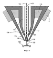
- Figure 1 schematically shows a prior art compound lens.
- Figure 1 schematically shows a beam of charged particles 102 travelling around particle-optical axis 104 and impinging on a sample 100.
- the sample is mounted on a sample carrier 122 that is movable with respect to the beam.
- the objective lens comprises a magnetic yoke with two pole pieces 106 and 108 guiding the magnetic field generated with coil 110 to an area near the beam.
- the yoke is electrically connected to ground.
- the outer pole piece 106 also guides the magnetic field generated by coil 112 to the sample, thus generating an immersion field.
- Electrode 114 is formed as a tube surrounding the beam, ending with a face 116 facing the sample. Insulator 112 centers the tube within the magnetic yoke and electrically insulates the two.
- the tube and the face need not be one piece, or even one material. Important for its functioning as one electrode is that the parts are sufficiently electrically conductive and electrically connected to each other to form one electric surface.
- a sensitive surface such as a YAP:Ce or a YAG:Ce crystal is mounted on the face 116 .
- the photons generated by the scintillator are detected with a photon detector.
- the scintillator should be formed as a disk with a central hole in it.
- the scintillator disk is preferably coated with a thin (10-100 nm) layer of aluminium, the coating forming a conductive layer and the coating reflecting photons that otherwise would emerge from the scintillator in the direction of the sample.
- a second charged particle detector 120 is located in an electrically field free region within the second electrode. This second detector may, for example, be a solid state electron detector, or a detector comprising a scintillator and photon detector. It is noted that magnetic deflectors can be placed in, for example, area 118 between the inner yoke and the second electrode.
- the sensitive surface may, instead of being a scintillator based detector as described above, also be a semiconductor based detector, e.g. a pixilated CMOS detector or a segmented photodetector.
- the primary electrons when impinging on the sample, cause the emission of secondary radiation, including backscattered electrons (BSEs) and secondary electrons (SEs). From a detection point of view the difference between these two is that an SE is often defined as an electron emerging from the sample with an energy of less than 50 eV, many of those with an energy of less than 5 eV, while a BSE emerges from the sample with an energy above 50 eV (up to the energy of the primary beam).
- the electric field between the sample and the second electrode directs both these electrons towards the direction of face 116, and the electrons enter the magnetic immersion field breaking out of the lens.
- the low energy electrons (all SEs and a small part of the BSEs) are kept so close to the axis that they travel through the hole in face 116 and enter the field free region within the second electrode. Many of these electrons are then detected by detector 120.
- the back-scattered electrons with a large energy for example an energy in excess of 80% of the energy of the primary electrons, are less confined by the combined effect of the electrostatic and magnetic field and hit the face 116, and thus the scintillator, thereby generating photons to be detected by a photon detector.
- Figure 2 schematically shows a detail of a compound lens according to the invention.
- FIG. 2 schematically shows the sample 100, the tip of lens pole 106, the extremity of the electrode 114, with the detector and beam 102.
- the detector is now split in three annular rings 205, 206 and 207.
- a first group of BSE's comprising BSE 202, impinge on ring 205, a second group of BSE's, including BSE 203, impinge on ring 206 and a third group of BSE's, including BSE 204 impinge on ring 207.
- BSE's comprising BSE 202, impinge on ring 205
- BSE 203 impinge on ring 206
- BSE 204 impinge on ring 207.
- the, in this case three, groups of BSE's can be measured separately from each other.
- the three groups have different combinations of ⁇ (the angle relative to the perpendicular to the surface of the sample with which the BSE emerges from the sample) and E (the energy with which the BSE emerges from the sample).
- ⁇ the angle relative to the perpendicular to the surface of the sample with which the BSE emerges from the sample
- E the energy with which the BSE emerges from the sample.
- Figure 3 schematically shows a detector for use in the compound lens according to the invention.
- Figure 3 not only shows a detector in which the sensitive parts are arranged as annular segments.
- the sensitive parts are arranged as annular segments.
- Around central hole 208 three annular segments, three segments 205-1...205-3 are arranged, surrounded by a second group of segments 206-1...206-3 and a third group of segments 207-1...207-3, each group of segments forming an annulus.
- This detector not only enables, for example, material contrast, but, as clear to the skilled artisan, topological contrast resulting in non-circle symmetric distribution of the BSE's over the detector annuli.
- a compound objective lens for a Scanning Electron Microscope comprising a conventional magnetic lens excited by lens coil 110, an immersion magnetic lens excited by lens coil 112, and an immersion electrostatic lens excited by the voltage difference between the sample 100 and electrode 114.
- the electron beam 102 can be focused on the sample using several combinations of excitations of coils 110 and 112.
- An electron detector (116) is positioned close to the sample (100) to detect backscattered electrons (BSE's). Inventors found that more information of the BSE's could be obtained when the detector can distinguish between BSE's that strike the detector close to the axis and BSE's that strike the detector further removed from the axis.
- the compound lens can be made to function as an energy selective detector
Landscapes
- Chemical & Material Sciences (AREA)
- Analytical Chemistry (AREA)
- Analysing Materials By The Use Of Radiation (AREA)
Abstract
Description
- The invention relates to a method of forming an image of a sample at a sample position by scanning a finely focused beam of charged particles over the sample, as a result of which backscattered electrons emerge from the sample, the image formed by detecting backscattered electrons, the beam focused by a compound charged particle lens, the compound lens showing
- a symmetry axis;
- a first magnetic lens pole near the sample position and a second magnetic lens pole more removed from the sample position;
- a first coil for generating a focusing magnetic field between the first magnetic lens pole and the second magnetic lens pole
- a second lens coil for generating a focusing immersion magnetic field between the first magnetic lens pole and the sample position; and
- an electrode with a central hole, the central hole for passing the beam of charged particles through the lens to the sample, the electrode for generating a decelerating electric field between the lens and the sample by applying a voltage difference between the electrode and the sample;
the compound lens thus having at least three parameters to determine the focal strength of the compound lens;
the compound lens comprising an electron detector showing a sensitive surface with a central hole, the sensitive surface coinciding with and electrically forming a part of the electrode;
the method comprising - exciting the immersion coil, the lens coil and the decelerating electric field of the compound lens so that
- ○ the finely focused beam is focused at the sample; and
- ○ the voltage difference of the sample is a predetermined voltage difference; and
- detecting backscattered electrons impacting on the detector, the backscattered electrons emerging from the sample with a selected angle α and a selected energy E, with α the angle with which the backscattered electrons leave the sample with respect to the symmetry axis of the compound lens, and E the energy with which the backscattered electrons leave the sample.
- The invention also relates to a compound charged particle lens equipped to perform the method.
- Such a method is inter alia known from European Patent Application
EP12165423 - A SEM column comprises an electron source for producing an electron beam with a selectable energy of, for example, between 200 eV and 30 keV, lenses to manipulate (focus, magnify, demagnify) the electron beam, deflectors for deflecting and centering the beam, and an objective lens to focus the beam on a sample. The objective lens may for example be a simple magnetic lens, an immersion lens in which the sample is immersed in a magnetic field, or a compound lens as described here. Advantages of such a compound lens, as known to the person skilled in the art, are for example improved resolution at low energies due to the decelerating electrostatic field, improved resolution due to the immersion magnetic field. However, not all samples can be viewed with all 'modes' of such a compound lens: for example a magnetisable sample, such as old fashioned audiotape or videotape, cannot be viewed in an immersion magnetic field without changing the magnetic properties of the sample.
- As the compound lens has at least three degrees determining the focal length of the lens, several combinations of electrostatic field, magnetic immersion field (governed by the excitation of the first coil) and focusing magnetic field (governed by the excitation of the second coil) can be used to form a focus on the sample. In many cases the electrostatic field is used to determine the energy with which the electrons impact on the sample. Even then a range of combinations of excitation of the first and the second coil can be used to form the focus at the appropriate location.
- When electrons impinge on a sample, secondary radiation is formed. Most importantly secondary electrons (SE's) are formed, exiting the sample with an energy of less than 50 eV, and backscattered electrons (BSE's) are formed, exiting the sample with an energy in excess of 50 eV.
- Assuming the compound lens uses an electrostatic field that decelerates the impinging beam, the direction of the electrostatic field is defined: the SE's are accelerated to the lens and pass through the hole in the electrode. This is the normal mode in which the compound lens is used.
- It is noted that the SE's can be detected by a detector between the electrode and the electron source.
- BSE's leave the sample with an energy from e.g. 50 eV up to an energy equal to the energy with which the impinging electrons land on the sample, for example 10 keV or more. The BSE's emerge from the sample under an angle α relative to the normal to the sample's surface, and an energy E. As known to the person skilled in the art the statistical distribution of this angle and energy is a function of sample material and beam energy.
- There is a demand for a configurable compound lens with electron detector that gives information for energy and/or angle distribution of BSE's.
- To that end a method of using the compound lens with the electron detector is
-
- the electron detector is equipped to distinguish backscattered electrons of a first group and a second group, the first group impacting on the detector closer to the symmetry axis than the second group, the backscattered electrons from the first group having different combinations of α and E than electrons of the second group; and
- the ratio of excitation of the first coil and the second coil is used to control the part of the backscattered electrons belonging to the first group and the part of the backscattered electrons belonging to the second group, while keeping the focus on the sample.
- The invention is based on the insight that several ratios (or combinations) of excitation of the first and the second coil, each ratio resulting in a beam focused on the sample. However, different ratios result in a different radial distribution of BSE's over the detector. By now forming the detector such that the detector can give information of the distance from the axis that the detected electrons impact the detector, additional information about the BSE's is gathered.
- Preferably this is done by equipping the detector with two or more annular detector areas (sensitive areas).
- However, also a pixilated detector, such as a CMOS chip, can be used as the data from such a detector can be processed to resemble the data of two or more annular areas.
- It is noted that some BSE's will pass through the hole of the detector/electrode surface. Such electrons can be detected by a detector between the electron source and the detector/electrode. Such detectors are known, e.g. the detector from US patent number
US6,646,261 . - It is mentioned that the detector can be a semiconductor detector, but also a scintillator based detector, using for example a SiPMT, or a conventional PMT, with or without light guides.
- The foregoing has outlined rather broadly the features and technical advantages of the present invention in order that the detailed description of the invention that follows may be better understood. Additional features and advantages of the invention will be described hereinafter. It should be appreciated by those skilled in the art that the conception and specific embodiments disclosed may be readily utilized as a basis for modifying or designing other structures for carrying out the same purposes of the present invention. It should also be realized by those skilled in the art that such equivalent constructions do not depart from the invention as set forth in the appended claims.
- For a more thorough understanding of the present invention, and advantages thereof, the invention is explained using figures, in which identical reference numerals indicate corresponding features.
- To that end:
-
Figure 1 schematically shows a prior art compound lens; -
Figure 2 schematically shows a detail of a compound lens according to the invention; and -
Figure 3 schematically shows a detector for use in the compound lens according to the invention. -
Figure 1 schematically shows a prior art compound lens. -
Figure 1 schematically shows a beam ofcharged particles 102 travelling around particle-optical axis 104 and impinging on asample 100. The sample is mounted on asample carrier 122 that is movable with respect to the beam. The objective lens comprises a magnetic yoke with twopole pieces coil 110 to an area near the beam. The yoke is electrically connected to ground. Theouter pole piece 106 also guides the magnetic field generated bycoil 112 to the sample, thus generating an immersion field. Electrode 114 is formed as a tube surrounding the beam, ending with aface 116 facing the sample.Insulator 112 centers the tube within the magnetic yoke and electrically insulates the two. - It is noted that the tube and the face need not be one piece, or even one material. Important for its functioning as one electrode is that the parts are sufficiently electrically conductive and electrically connected to each other to form one electric surface.
On the face 116 a sensitive surface, such as a YAP:Ce or a YAG:Ce crystal is mounted. The photons generated by the scintillator are detected with a photon detector. As is clear from the figure, the scintillator should be formed as a disk with a central hole in it.
It is noted that the scintillator disk is preferably coated with a thin (10-100 nm) layer of aluminium, the coating forming a conductive layer and the coating reflecting photons that otherwise would emerge from the scintillator in the direction of the sample.
A second chargedparticle detector 120 is located in an electrically field free region within the second electrode. This second detector may, for example, be a solid state electron detector, or a detector comprising a scintillator and photon detector.
It is noted that magnetic deflectors can be placed in, for example,area 118 between the inner yoke and the second electrode. - It is noted that the sensitive surface may, instead of being a scintillator based detector as described above, also be a semiconductor based detector, e.g. a pixilated CMOS detector or a segmented photodetector.
- It is also noted that it is known to further decelerate the beam between the
first electrode 106 and the sample position by biasing the sample to a positive energy. - The primary electrons, when impinging on the sample, cause the emission of secondary radiation, including backscattered electrons (BSEs) and secondary electrons (SEs). From a detection point of view the difference between these two is that an SE is often defined as an electron emerging from the sample with an energy of less than 50 eV, many of those with an energy of less than 5 eV, while a BSE emerges from the sample with an energy above 50 eV (up to the energy of the primary beam). The electric field between the sample and the second electrode directs both these electrons towards the direction of
face 116, and the electrons enter the magnetic immersion field breaking out of the lens. The low energy electrons (all SEs and a small part of the BSEs) are kept so close to the axis that they travel through the hole inface 116 and enter the field free region within the second electrode. Many of these electrons are then detected bydetector 120.
The back-scattered electrons with a large energy, for example an energy in excess of 80% of the energy of the primary electrons, are less confined by the combined effect of the electrostatic and magnetic field and hit theface 116, and thus the scintillator, thereby generating photons to be detected by a photon detector. - Due to the potential difference between the sample and the electrode, the BSEs impinge on the scintillator with an energy of several keV. Using the lens shown in
figure 1 , a grounded sample and first electrode (and yoke) and a potential of approximately +8 kV on the electrode, a detection efficiency for BSEs of 85% is obtained, depending on working distance (distance between sample and first pole piece), landing energy and BSE energy (influenced by for example a bias voltage between sample and first pole piece). -
Figure 2 schematically shows a detail of a compound lens according to the invention. -
Figure 2 schematically shows thesample 100, the tip oflens pole 106, the extremity of theelectrode 114, with the detector andbeam 102. The detector is now split in threeannular rings BSE 202, impinge onring 205, a second group of BSE's, includingBSE 203, impinge onring 206 and a third group of BSE's, includingBSE 204 impinge onring 207. Hereby the, in this case three, groups of BSE's can be measured separately from each other. The three groups have different combinations of α (the angle relative to the perpendicular to the surface of the sample with which the BSE emerges from the sample) and E (the energy with which the BSE emerges from the sample). Using this detector information, such as material contrast, can be obtained. -
Figure 3 schematically shows a detector for use in the compound lens according to the invention. -
Figure 3 not only shows a detector in which the sensitive parts are arranged as annular segments. Aroundcentral hole 208 three annular segments, three segments 205-1...205-3 are arranged, surrounded by a second group of segments 206-1...206-3 and a third group of segments 207-1...207-3, each group of segments forming an annulus. - This detector not only enables, for example, material contrast, but, as clear to the skilled artisan, topological contrast resulting in non-circle symmetric distribution of the BSE's over the detector annuli.
- So, in conclusion: a compound objective lens for a Scanning Electron Microscope, the lens comprising a conventional magnetic lens excited by
lens coil 110, an immersion magnetic lens excited bylens coil 112, and an immersion electrostatic lens excited by the voltage difference between thesample 100 andelectrode 114. For a predetermined excitation of the electrostatic immersion lens theelectron beam 102 can be focused on the sample using several combinations of excitations ofcoils - An electron detector (116) is positioned close to the sample (100) to detect backscattered electrons (BSE's). Inventors found that more information of the BSE's could be obtained when the detector can distinguish between BSE's that strike the detector close to the axis and BSE's that strike the detector further removed from the axis.
- Inventors found that, by tuning the ratio of the excitation of the
coils
Claims (5)
- Method of forming an image of a sample (100) at a sample position by scanning a finely focused beam of charged particles (102) over the sample, as a result of which backscattered electrons emerge from the sample, the image formed by detecting backscattered electrons, the beam focused by a compound charged particle lens, the compound lens showing• a symmetry axis (104);• a first magnetic lens pole (106) near the sample position and a second magnetic lens pole (108) more removed from the sample position;• a first coil (110) for generating a focusing magnetic field between the first magnetic lens pole and the second magnetic lens pole;• a second lens coil (112) for generating a focusing immersion magnetic field between the first magnetic lens pole and the sample position; and• an electrode (114) with a central hole, the central hole for passing the beam of charged particles through the lens to the sample, the electrode for generating a decelerating electric field between the lens and the sample by applying a voltage difference between the electrode and the sample;
the compound lens thus having at least three parameters to determine the focal strength of the compound lens;
the compound lens comprising an electron detector showing a sensitive surface (116) with a central hole, the sensitive surface coinciding with and electrically forming a part of the electrode;
the method comprising• exciting the immersion coil, the lens coil and the decelerating electric field of the compound lens so that
○ the finely focused beam is focused at the sample; and
○ the voltage difference of the sample is a predetermined voltage difference;
and• detecting backscattered electrons impacting on the detector, the backscattered electrons emerging from the sample with a selected angle α and a selected energy E, with α the angle with which the backscattered electrons leave the sample with respect to the symmetry axis of the compound lens, and E the energy with which the backscattered electrons leave the sample;
characterized in that• the electron detector is equipped to distinguish backscattered electrons of a first group and a second group, the first group impacting on the detector closer to the symmetry axis than the second group, the backscattered electrons from the first group having different combinations of α and E than electrons of the second group; and• the ratio of exciting the first coil and the second coil is used to control the part of the backscattered electrons belonging to the first group and the part of the backscattered electrons belonging to the second group, while keeping the beam focused on the sample. - The method of claim 1 in which the detector is a detector equipped with two or more annular detection areas, one of the annular detection areas for detecting electrons from the first group and the other annular detection area for detecting electrons from the second group.
- The method of claim 1 in which the detector is a pixilated detector, and the signal of a first group of pixels is combined to give a first signal and the signal of a second group of pixels is combined to give a second signal, the first signal proportional to the amount of impinging electrons of the first group and the second signal proportional to the amount of impinging electrons of the second group.
- The method of any of the preceding claims in which a second detector is positioned further removed from the sample position than the detector coinciding with the electrode, the second detector giving a signal proportional to a third group of backscattered electrons, the third group of backscattered electrons passing through the central hole.
- Compound charged particle lens, the compound lens showing• a symmetry axis;• a first magnetic lens pole (104) near the sample position and a second magnetic lens pole (106) more removed from the sample position;• an immersion coil (108) for generating a focusing magnetic field between the first magnetic lens pole (104) and the sample position;• a lens coil (110) for generating a focusing magnetic field between the first magnetic lens pole (104) and the second magnetic lens pole (106);• an electrode (112) with a central hole, the central hole for passing the beam of charged particles through the lens to the sample, the electrode for generating a decelerating electric field between the lens and the sample by applying a voltage difference between the electrode and the sample;
the compound lens thus having at least three parameters to determine the focal strength of the compound lens;
the compound lens comprising an electron detector showing a sensitive surface (116) with a central hole, the sensitive surface coinciding with the electrode
characterized in that• the detector is equipped to distinguish between impinging backscattered electrons from a first group and a second group, the first group impinging closer to the axis than the second group.
Priority Applications (4)
| Application Number | Priority Date | Filing Date | Title |
|---|---|---|---|
| EP12183662.1A EP2706554B1 (en) | 2012-09-10 | 2012-09-10 | Method of using a compound particle-optical lens |
| JP2013185068A JP6239322B2 (en) | 2012-09-10 | 2013-09-06 | Method of using composite particle optical lens |
| CN201310405430.7A CN103681186B (en) | 2012-09-10 | 2013-09-09 | Method of using a compound particle-optical lens |
| US14/021,480 US9490100B2 (en) | 2012-09-10 | 2013-09-09 | Method of using a compound particle-optical lens |
Applications Claiming Priority (1)
| Application Number | Priority Date | Filing Date | Title |
|---|---|---|---|
| EP12183662.1A EP2706554B1 (en) | 2012-09-10 | 2012-09-10 | Method of using a compound particle-optical lens |
Publications (2)
| Publication Number | Publication Date |
|---|---|
| EP2706554A1 true EP2706554A1 (en) | 2014-03-12 |
| EP2706554B1 EP2706554B1 (en) | 2016-05-25 |
Family
ID=46939554
Family Applications (1)
| Application Number | Title | Priority Date | Filing Date |
|---|---|---|---|
| EP12183662.1A Active EP2706554B1 (en) | 2012-09-10 | 2012-09-10 | Method of using a compound particle-optical lens |
Country Status (4)
| Country | Link |
|---|---|
| US (1) | US9490100B2 (en) |
| EP (1) | EP2706554B1 (en) |
| JP (1) | JP6239322B2 (en) |
| CN (1) | CN103681186B (en) |
Cited By (2)
| Publication number | Priority date | Publication date | Assignee | Title |
|---|---|---|---|---|
| CN110376229A (en) * | 2019-06-12 | 2019-10-25 | 聚束科技(北京)有限公司 | The scanning electron microscope and sample detection method for having combined type detection system |
| WO2021204740A1 (en) * | 2020-04-10 | 2021-10-14 | Asml Netherlands B.V. | Charged particle beam apparatus with multiple detectors and methods for imaging |
Families Citing this family (11)
| Publication number | Priority date | Publication date | Assignee | Title |
|---|---|---|---|---|
| US9190241B2 (en) * | 2013-03-25 | 2015-11-17 | Hermes-Microvision, Inc. | Charged particle beam apparatus |
| EP3161851B1 (en) * | 2014-06-27 | 2018-08-15 | Gatan, Inc. | Electron energy loss spectrometer |
| US10236156B2 (en) | 2015-03-25 | 2019-03-19 | Hermes Microvision Inc. | Apparatus of plural charged-particle beams |
| US10297418B2 (en) * | 2015-07-14 | 2019-05-21 | ICT Integrated Circuit Testing Gesellschaft für Halbleiterprüftechnik mbH | Method of reducing coma and chromatic aberration in a charged particle beam device, and charged particle beam device |
| IL267670B2 (en) * | 2016-12-30 | 2025-10-01 | Asml Netherlands Bv | An apparatus using multiple charged particle beams |
| JP6741858B2 (en) * | 2017-03-24 | 2020-08-19 | 株式会社日立ハイテク | Charged particle beam device |
| US10777382B2 (en) | 2017-11-21 | 2020-09-15 | Focus-Ebeam Technology (Beijing) Co., Ltd. | Low voltage scanning electron microscope and method for specimen observation |
| EP3525229A1 (en) * | 2018-02-13 | 2019-08-14 | Universiteit Maastricht | Incident particle localization method and system |
| JP7085258B2 (en) * | 2018-04-13 | 2022-06-16 | 株式会社ホロン | Ultra-high-speed electron detector and scanning electron beam inspection device incorporating the detector |
| CN114256043B (en) | 2020-12-02 | 2024-04-05 | 聚束科技(北京)有限公司 | An electron beam system |
| CN114220725B (en) | 2020-12-02 | 2024-05-07 | 聚束科技(北京)有限公司 | Electron microscope |
Citations (5)
| Publication number | Priority date | Publication date | Assignee | Title |
|---|---|---|---|---|
| DE19845329A1 (en) * | 1998-03-10 | 1999-09-23 | Erik Essers | Scanning electron microscope for acquiring images of specimens in high pressure chamber |
| EP1216542A1 (en) | 1999-09-29 | 2002-06-26 | Mobilian Corporation | Multiple wireless communication protocol methods and apparatuses including quality of service considerations |
| US20030127595A1 (en) * | 1998-03-02 | 2003-07-10 | Hitachi, Ltd. | Method and apparatus for scanning transmission electron microscopy |
| US6646261B2 (en) | 2000-12-22 | 2003-11-11 | Jan Martijn Krans | SEM provided with a secondary electron detector having a central electrode |
| US20060054814A1 (en) * | 2003-07-30 | 2006-03-16 | Dror Shemesh | Scanning electron microscope having multiple detectors and a method for multiple detector based imaging |
Family Cites Families (11)
| Publication number | Priority date | Publication date | Assignee | Title |
|---|---|---|---|---|
| US4897545A (en) * | 1987-05-21 | 1990-01-30 | Electroscan Corporation | Electron detector for use in a gaseous environment |
| US5866905A (en) * | 1991-05-15 | 1999-02-02 | Hitachi, Ltd. | Electron microscope |
| US6590210B1 (en) | 1998-03-10 | 2003-07-08 | Erik Essers | Scanning electron microscope |
| GB2348048A (en) * | 1999-03-19 | 2000-09-20 | Shimadzu Research Lab | Magnetic immersion lenses |
| NL1023260C1 (en) | 2003-04-24 | 2004-10-27 | Fei Co | Particle-optical device with a permanent magnetic lens and an electrostatic lens. |
| CN2779548Y (en) * | 2005-03-09 | 2006-05-10 | 浙江大学 | Solid immersion lens |
| JP4822925B2 (en) * | 2006-04-28 | 2011-11-24 | 日本電子株式会社 | Transmission electron microscope |
| JP4597207B2 (en) * | 2008-03-31 | 2010-12-15 | 株式会社日立ハイテクノロジーズ | Scanning electron microscope |
| JP5386596B2 (en) * | 2010-01-20 | 2014-01-15 | 株式会社日立ハイテクノロジーズ | Charged particle beam equipment |
| DE102010026169B4 (en) * | 2010-07-06 | 2014-09-04 | Carl Zeiss Microscopy Gmbh | A particle beam system |
| EP2518755B1 (en) | 2011-04-26 | 2014-10-15 | FEI Company | In-column detector for particle-optical column |
-
2012
- 2012-09-10 EP EP12183662.1A patent/EP2706554B1/en active Active
-
2013
- 2013-09-06 JP JP2013185068A patent/JP6239322B2/en active Active
- 2013-09-09 CN CN201310405430.7A patent/CN103681186B/en active Active
- 2013-09-09 US US14/021,480 patent/US9490100B2/en active Active
Patent Citations (5)
| Publication number | Priority date | Publication date | Assignee | Title |
|---|---|---|---|---|
| US20030127595A1 (en) * | 1998-03-02 | 2003-07-10 | Hitachi, Ltd. | Method and apparatus for scanning transmission electron microscopy |
| DE19845329A1 (en) * | 1998-03-10 | 1999-09-23 | Erik Essers | Scanning electron microscope for acquiring images of specimens in high pressure chamber |
| EP1216542A1 (en) | 1999-09-29 | 2002-06-26 | Mobilian Corporation | Multiple wireless communication protocol methods and apparatuses including quality of service considerations |
| US6646261B2 (en) | 2000-12-22 | 2003-11-11 | Jan Martijn Krans | SEM provided with a secondary electron detector having a central electrode |
| US20060054814A1 (en) * | 2003-07-30 | 2006-03-16 | Dror Shemesh | Scanning electron microscope having multiple detectors and a method for multiple detector based imaging |
Cited By (3)
| Publication number | Priority date | Publication date | Assignee | Title |
|---|---|---|---|---|
| CN110376229A (en) * | 2019-06-12 | 2019-10-25 | 聚束科技(北京)有限公司 | The scanning electron microscope and sample detection method for having combined type detection system |
| US11145487B2 (en) | 2019-06-12 | 2021-10-12 | Focus-Ebeam Technology (Beijing) Co., Ltd. | Scanning electron microscope with composite detection system and specimen detection method |
| WO2021204740A1 (en) * | 2020-04-10 | 2021-10-14 | Asml Netherlands B.V. | Charged particle beam apparatus with multiple detectors and methods for imaging |
Also Published As
| Publication number | Publication date |
|---|---|
| CN103681186B (en) | 2017-03-22 |
| US20140070098A1 (en) | 2014-03-13 |
| EP2706554B1 (en) | 2016-05-25 |
| US9490100B2 (en) | 2016-11-08 |
| CN103681186A (en) | 2014-03-26 |
| JP2014053306A (en) | 2014-03-20 |
| JP6239322B2 (en) | 2017-11-29 |
Similar Documents
| Publication | Publication Date | Title |
|---|---|---|
| EP2706554B1 (en) | Method of using a compound particle-optical lens | |
| EP2518755B1 (en) | In-column detector for particle-optical column | |
| TWI382442B (en) | An electron beam appartus | |
| JP5860642B2 (en) | Scanning electron microscope | |
| US6392231B1 (en) | Swinging objective retarding immersion lens electron optics focusing, deflection and signal collection system and method | |
| US20210110994A1 (en) | Scanning electron microscope objective lens system and method for specimen observation | |
| US9601303B2 (en) | Charged particle beam device and method for inspecting and/or imaging a sample | |
| EP2511939B1 (en) | Arrangement and method for the contrast improvement in a charged particle beam device for inspecting a specimen | |
| JP3723260B2 (en) | Particle beam column | |
| US8629395B2 (en) | Charged particle beam apparatus | |
| JP6880209B2 (en) | Scanning electron microscope | |
| EP1288996B1 (en) | Particle beam apparatus | |
| US6646261B2 (en) | SEM provided with a secondary electron detector having a central electrode | |
| EP2219204B1 (en) | Arrangement and method for the contrast improvement in a charged particle beam device for inspecting a specimen | |
| US6570163B1 (en) | Electron detectors | |
| KR100813210B1 (en) | System and Method for Electro-optical Focusing, Detection and Signal Acquisition of Vibration Delay Immersion Objective Lens | |
| WO2025202056A1 (en) | Multi electron-beam system for inspection with backscattered electrons | |
| EP2833390A1 (en) | Use of electrostatic objective lens in an electron microscope |
Legal Events
| Date | Code | Title | Description |
|---|---|---|---|
| PUAI | Public reference made under article 153(3) epc to a published international application that has entered the european phase |
Free format text: ORIGINAL CODE: 0009012 |
|
| AK | Designated contracting states |
Kind code of ref document: A1 Designated state(s): AL AT BE BG CH CY CZ DE DK EE ES FI FR GB GR HR HU IE IS IT LI LT LU LV MC MK MT NL NO PL PT RO RS SE SI SK SM TR |
|
| AX | Request for extension of the european patent |
Extension state: BA ME |
|
| 17P | Request for examination filed |
Effective date: 20140820 |
|
| RBV | Designated contracting states (corrected) |
Designated state(s): AL AT BE BG CH CY CZ DE DK EE ES FI FR GB GR HR HU IE IS IT LI LT LU LV MC MK MT NL NO PL PT RO RS SE SI SK SM TR |
|
| GRAP | Despatch of communication of intention to grant a patent |
Free format text: ORIGINAL CODE: EPIDOSNIGR1 |
|
| RIC1 | Information provided on ipc code assigned before grant |
Ipc: H01J 37/145 20060101AFI20160115BHEP Ipc: H01J 37/28 20060101ALI20160115BHEP |
|
| INTG | Intention to grant announced |
Effective date: 20160209 |
|
| GRAS | Grant fee paid |
Free format text: ORIGINAL CODE: EPIDOSNIGR3 |
|
| GRAA | (expected) grant |
Free format text: ORIGINAL CODE: 0009210 |
|
| AK | Designated contracting states |
Kind code of ref document: B1 Designated state(s): AL AT BE BG CH CY CZ DE DK EE ES FI FR GB GR HR HU IE IS IT LI LT LU LV MC MK MT NL NO PL PT RO RS SE SI SK SM TR |
|
| REG | Reference to a national code |
Ref country code: GB Ref legal event code: FG4D |
|
| REG | Reference to a national code |
Ref country code: CH Ref legal event code: EP |
|
| REG | Reference to a national code |
Ref country code: IE Ref legal event code: FG4D Ref country code: AT Ref legal event code: REF Ref document number: 802948 Country of ref document: AT Kind code of ref document: T Effective date: 20160615 |
|
| REG | Reference to a national code |
Ref country code: DE Ref legal event code: R096 Ref document number: 602012018897 Country of ref document: DE |
|
| REG | Reference to a national code |
Ref country code: LT Ref legal event code: MG4D Ref country code: FR Ref legal event code: PLFP Year of fee payment: 5 |
|
| REG | Reference to a national code |
Ref country code: NL Ref legal event code: MP Effective date: 20160525 |
|
| PG25 | Lapsed in a contracting state [announced via postgrant information from national office to epo] |
Ref country code: NO Free format text: LAPSE BECAUSE OF FAILURE TO SUBMIT A TRANSLATION OF THE DESCRIPTION OR TO PAY THE FEE WITHIN THE PRESCRIBED TIME-LIMIT Effective date: 20160825 Ref country code: LT Free format text: LAPSE BECAUSE OF FAILURE TO SUBMIT A TRANSLATION OF THE DESCRIPTION OR TO PAY THE FEE WITHIN THE PRESCRIBED TIME-LIMIT Effective date: 20160525 Ref country code: NL Free format text: LAPSE BECAUSE OF FAILURE TO SUBMIT A TRANSLATION OF THE DESCRIPTION OR TO PAY THE FEE WITHIN THE PRESCRIBED TIME-LIMIT Effective date: 20160525 Ref country code: FI Free format text: LAPSE BECAUSE OF FAILURE TO SUBMIT A TRANSLATION OF THE DESCRIPTION OR TO PAY THE FEE WITHIN THE PRESCRIBED TIME-LIMIT Effective date: 20160525 |
|
| REG | Reference to a national code |
Ref country code: AT Ref legal event code: MK05 Ref document number: 802948 Country of ref document: AT Kind code of ref document: T Effective date: 20160525 |
|
| PG25 | Lapsed in a contracting state [announced via postgrant information from national office to epo] |
Ref country code: ES Free format text: LAPSE BECAUSE OF FAILURE TO SUBMIT A TRANSLATION OF THE DESCRIPTION OR TO PAY THE FEE WITHIN THE PRESCRIBED TIME-LIMIT Effective date: 20160525 Ref country code: GR Free format text: LAPSE BECAUSE OF FAILURE TO SUBMIT A TRANSLATION OF THE DESCRIPTION OR TO PAY THE FEE WITHIN THE PRESCRIBED TIME-LIMIT Effective date: 20160826 Ref country code: RS Free format text: LAPSE BECAUSE OF FAILURE TO SUBMIT A TRANSLATION OF THE DESCRIPTION OR TO PAY THE FEE WITHIN THE PRESCRIBED TIME-LIMIT Effective date: 20160525 Ref country code: PT Free format text: LAPSE BECAUSE OF FAILURE TO SUBMIT A TRANSLATION OF THE DESCRIPTION OR TO PAY THE FEE WITHIN THE PRESCRIBED TIME-LIMIT Effective date: 20160926 Ref country code: SE Free format text: LAPSE BECAUSE OF FAILURE TO SUBMIT A TRANSLATION OF THE DESCRIPTION OR TO PAY THE FEE WITHIN THE PRESCRIBED TIME-LIMIT Effective date: 20160525 Ref country code: LV Free format text: LAPSE BECAUSE OF FAILURE TO SUBMIT A TRANSLATION OF THE DESCRIPTION OR TO PAY THE FEE WITHIN THE PRESCRIBED TIME-LIMIT Effective date: 20160525 |
|
| PG25 | Lapsed in a contracting state [announced via postgrant information from national office to epo] |
Ref country code: IT Free format text: LAPSE BECAUSE OF FAILURE TO SUBMIT A TRANSLATION OF THE DESCRIPTION OR TO PAY THE FEE WITHIN THE PRESCRIBED TIME-LIMIT Effective date: 20160525 |
|
| PG25 | Lapsed in a contracting state [announced via postgrant information from national office to epo] |
Ref country code: EE Free format text: LAPSE BECAUSE OF FAILURE TO SUBMIT A TRANSLATION OF THE DESCRIPTION OR TO PAY THE FEE WITHIN THE PRESCRIBED TIME-LIMIT Effective date: 20160525 Ref country code: DK Free format text: LAPSE BECAUSE OF FAILURE TO SUBMIT A TRANSLATION OF THE DESCRIPTION OR TO PAY THE FEE WITHIN THE PRESCRIBED TIME-LIMIT Effective date: 20160525 Ref country code: CZ Free format text: LAPSE BECAUSE OF FAILURE TO SUBMIT A TRANSLATION OF THE DESCRIPTION OR TO PAY THE FEE WITHIN THE PRESCRIBED TIME-LIMIT Effective date: 20160525 Ref country code: RO Free format text: LAPSE BECAUSE OF FAILURE TO SUBMIT A TRANSLATION OF THE DESCRIPTION OR TO PAY THE FEE WITHIN THE PRESCRIBED TIME-LIMIT Effective date: 20160525 Ref country code: SK Free format text: LAPSE BECAUSE OF FAILURE TO SUBMIT A TRANSLATION OF THE DESCRIPTION OR TO PAY THE FEE WITHIN THE PRESCRIBED TIME-LIMIT Effective date: 20160525 |
|
| PG25 | Lapsed in a contracting state [announced via postgrant information from national office to epo] |
Ref country code: PL Free format text: LAPSE BECAUSE OF FAILURE TO SUBMIT A TRANSLATION OF THE DESCRIPTION OR TO PAY THE FEE WITHIN THE PRESCRIBED TIME-LIMIT Effective date: 20160525 Ref country code: AT Free format text: LAPSE BECAUSE OF FAILURE TO SUBMIT A TRANSLATION OF THE DESCRIPTION OR TO PAY THE FEE WITHIN THE PRESCRIBED TIME-LIMIT Effective date: 20160525 Ref country code: BE Free format text: LAPSE BECAUSE OF NON-PAYMENT OF DUE FEES Effective date: 20160525 Ref country code: SM Free format text: LAPSE BECAUSE OF FAILURE TO SUBMIT A TRANSLATION OF THE DESCRIPTION OR TO PAY THE FEE WITHIN THE PRESCRIBED TIME-LIMIT Effective date: 20160525 |
|
| REG | Reference to a national code |
Ref country code: DE Ref legal event code: R097 Ref document number: 602012018897 Country of ref document: DE |
|
| PLBE | No opposition filed within time limit |
Free format text: ORIGINAL CODE: 0009261 |
|
| STAA | Information on the status of an ep patent application or granted ep patent |
Free format text: STATUS: NO OPPOSITION FILED WITHIN TIME LIMIT |
|
| PG25 | Lapsed in a contracting state [announced via postgrant information from national office to epo] |
Ref country code: MC Free format text: LAPSE BECAUSE OF FAILURE TO SUBMIT A TRANSLATION OF THE DESCRIPTION OR TO PAY THE FEE WITHIN THE PRESCRIBED TIME-LIMIT Effective date: 20160525 |
|
| REG | Reference to a national code |
Ref country code: CH Ref legal event code: PL |
|
| 26N | No opposition filed |
Effective date: 20170228 |
|
| GBPC | Gb: european patent ceased through non-payment of renewal fee |
Effective date: 20160910 |
|
| PG25 | Lapsed in a contracting state [announced via postgrant information from national office to epo] |
Ref country code: SI Free format text: LAPSE BECAUSE OF FAILURE TO SUBMIT A TRANSLATION OF THE DESCRIPTION OR TO PAY THE FEE WITHIN THE PRESCRIBED TIME-LIMIT Effective date: 20160525 |
|
| REG | Reference to a national code |
Ref country code: IE Ref legal event code: MM4A |
|
| PG25 | Lapsed in a contracting state [announced via postgrant information from national office to epo] |
Ref country code: CH Free format text: LAPSE BECAUSE OF NON-PAYMENT OF DUE FEES Effective date: 20160930 Ref country code: GB Free format text: LAPSE BECAUSE OF NON-PAYMENT OF DUE FEES Effective date: 20160910 Ref country code: LI Free format text: LAPSE BECAUSE OF NON-PAYMENT OF DUE FEES Effective date: 20160930 Ref country code: IE Free format text: LAPSE BECAUSE OF NON-PAYMENT OF DUE FEES Effective date: 20160910 |
|
| REG | Reference to a national code |
Ref country code: FR Ref legal event code: PLFP Year of fee payment: 6 |
|
| PG25 | Lapsed in a contracting state [announced via postgrant information from national office to epo] |
Ref country code: LU Free format text: LAPSE BECAUSE OF NON-PAYMENT OF DUE FEES Effective date: 20160910 |
|
| PG25 | Lapsed in a contracting state [announced via postgrant information from national office to epo] |
Ref country code: HU Free format text: LAPSE BECAUSE OF FAILURE TO SUBMIT A TRANSLATION OF THE DESCRIPTION OR TO PAY THE FEE WITHIN THE PRESCRIBED TIME-LIMIT; INVALID AB INITIO Effective date: 20120910 Ref country code: CY Free format text: LAPSE BECAUSE OF FAILURE TO SUBMIT A TRANSLATION OF THE DESCRIPTION OR TO PAY THE FEE WITHIN THE PRESCRIBED TIME-LIMIT Effective date: 20160525 |
|
| PG25 | Lapsed in a contracting state [announced via postgrant information from national office to epo] |
Ref country code: MT Free format text: LAPSE BECAUSE OF NON-PAYMENT OF DUE FEES Effective date: 20160930 Ref country code: HR Free format text: LAPSE BECAUSE OF FAILURE TO SUBMIT A TRANSLATION OF THE DESCRIPTION OR TO PAY THE FEE WITHIN THE PRESCRIBED TIME-LIMIT Effective date: 20160525 Ref country code: MK Free format text: LAPSE BECAUSE OF FAILURE TO SUBMIT A TRANSLATION OF THE DESCRIPTION OR TO PAY THE FEE WITHIN THE PRESCRIBED TIME-LIMIT Effective date: 20160525 Ref country code: IS Free format text: LAPSE BECAUSE OF FAILURE TO SUBMIT A TRANSLATION OF THE DESCRIPTION OR TO PAY THE FEE WITHIN THE PRESCRIBED TIME-LIMIT Effective date: 20160525 |
|
| PG25 | Lapsed in a contracting state [announced via postgrant information from national office to epo] |
Ref country code: BG Free format text: LAPSE BECAUSE OF FAILURE TO SUBMIT A TRANSLATION OF THE DESCRIPTION OR TO PAY THE FEE WITHIN THE PRESCRIBED TIME-LIMIT Effective date: 20160525 |
|
| REG | Reference to a national code |
Ref country code: FR Ref legal event code: PLFP Year of fee payment: 7 |
|
| PG25 | Lapsed in a contracting state [announced via postgrant information from national office to epo] |
Ref country code: AL Free format text: LAPSE BECAUSE OF FAILURE TO SUBMIT A TRANSLATION OF THE DESCRIPTION OR TO PAY THE FEE WITHIN THE PRESCRIBED TIME-LIMIT Effective date: 20160525 Ref country code: TR Free format text: LAPSE BECAUSE OF FAILURE TO SUBMIT A TRANSLATION OF THE DESCRIPTION OR TO PAY THE FEE WITHIN THE PRESCRIBED TIME-LIMIT Effective date: 20160525 |
|
| P01 | Opt-out of the competence of the unified patent court (upc) registered |
Effective date: 20230524 |
|
| PGFP | Annual fee paid to national office [announced via postgrant information from national office to epo] |
Ref country code: DE Payment date: 20250820 Year of fee payment: 14 |
|
| PGFP | Annual fee paid to national office [announced via postgrant information from national office to epo] |
Ref country code: FR Payment date: 20250912 Year of fee payment: 14 |