EP2706393A1 - Optical deflector including narrow piezoelectric sensor element between torsion bar and piezoelectric actuator - Google Patents
Optical deflector including narrow piezoelectric sensor element between torsion bar and piezoelectric actuator Download PDFInfo
- Publication number
- EP2706393A1 EP2706393A1 EP20130020089 EP13020089A EP2706393A1 EP 2706393 A1 EP2706393 A1 EP 2706393A1 EP 20130020089 EP20130020089 EP 20130020089 EP 13020089 A EP13020089 A EP 13020089A EP 2706393 A1 EP2706393 A1 EP 2706393A1
- Authority
- EP
- European Patent Office
- Prior art keywords
- piezoelectric sensor
- piezoelectric
- optical deflector
- support frame
- sensor element
- Prior art date
- Legal status (The legal status is an assumption and is not a legal conclusion. Google has not performed a legal analysis and makes no representation as to the accuracy of the status listed.)
- Granted
Links
Images







Classifications
-
- G—PHYSICS
- G02—OPTICS
- G02B—OPTICAL ELEMENTS, SYSTEMS OR APPARATUS
- G02B26/00—Optical devices or arrangements for the control of light using movable or deformable optical elements
- G02B26/08—Optical devices or arrangements for the control of light using movable or deformable optical elements for controlling the direction of light
- G02B26/10—Scanning systems
-
- G—PHYSICS
- G02—OPTICS
- G02B—OPTICAL ELEMENTS, SYSTEMS OR APPARATUS
- G02B26/00—Optical devices or arrangements for the control of light using movable or deformable optical elements
- G02B26/08—Optical devices or arrangements for the control of light using movable or deformable optical elements for controlling the direction of light
- G02B26/0816—Optical devices or arrangements for the control of light using movable or deformable optical elements for controlling the direction of light by means of one or more reflecting elements
- G02B26/0833—Optical devices or arrangements for the control of light using movable or deformable optical elements for controlling the direction of light by means of one or more reflecting elements the reflecting element being a micromechanical device, e.g. a MEMS mirror, DMD
- G02B26/0858—Optical devices or arrangements for the control of light using movable or deformable optical elements for controlling the direction of light by means of one or more reflecting elements the reflecting element being a micromechanical device, e.g. a MEMS mirror, DMD the reflecting means being moved or deformed by piezoelectric means
-
- H—ELECTRICITY
- H10—SEMICONDUCTOR DEVICES; ELECTRIC SOLID-STATE DEVICES NOT OTHERWISE PROVIDED FOR
- H10N—ELECTRIC SOLID-STATE DEVICES NOT OTHERWISE PROVIDED FOR
- H10N30/00—Piezoelectric or electrostrictive devices
- H10N30/101—Piezoelectric or electrostrictive devices with electrical and mechanical input and output, e.g. having combined actuator and sensor parts
Definitions
- the presently disclosed subject matter relates to an optical deflector used as a scanner in a projector, a bar code reader, a laser printer, a laser read amplifier, a head-up display apparatus or the like.
- an optical deflector is a micro electro mechanical system (MEMS) device manufactured by semiconductor manufacturing processes and micro machine technology.
- MEMS micro electro mechanical system
- a first prior art one-dimensional optical deflector is constructed by a circular mirror, a support frame surrounding the circular mirror, a pair of torsion bars connected between the support frame and the circular mirror, piezoelectric actuators provided between the support frame and the torsion bars for vibrating (rocking) the circular mirror through the torsion bars with respect to an axis of the circular mirror, and two semi-ring-shaped piezoelectric sensors provided at a circumference of the circular mirror for sensing rocking vibrations caused by the piezoelectric actuators (see: Fig. 1 of JP2011-150055 ).
- one piezoelectric sensor is provided between one of the torsion bars and one of the piezoelectric actuators on the same beam as that of the one of the piezoelectric actuators, thus solving all the problems of the above-described first prior art one-dimensional optical deflector (see: Figs. 16 , 17 and 18 of JP2010-197994A & US2010/0195180A1 ).
- the presently disclosed subject matter seeks to solve one or more of the above-described problems.
- an optical deflector including a mirror, a support frame surrounding the mirror, at least one torsion bar arranged along an axis of the mirror having an end coupled to an outer circumference of the mirror, a pair of piezoelectric actuators arranged between the support frame and the torsion bar, and a piezoelectric sensor inserted between the torsion bar and one of the piezoelectric actuators
- the piezoelectric sensor includes at least one piezoelectric sensor element the width thereof being smaller than two-fifths of the width of the one of the piezoelectric actuators and being arranged at a wide portion within two-fifths of the width from an inner end of the one of the piezoelectric actuators.
- a resonant state can be realized by the feedback control of a sense voltage of the piezoelectric sensor element to drive voltages of the piezoelectric actuators.
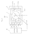
- a one-dimensional optical deflector 10A is constructed by a circular mirror 1 for reflecting a spotlight L from a laser diode 20, a rectangular support frame 2 surrounding the circular mirror 1, a pair of torsion bars 3-1 and 3-2 arranged along an X-axis of the circular mirror 1 coupled to the outer circumference of the circular mirror 1, a pair of linear piezoelectric actuators 4-1a and 4-1b arranged between the rectangular support frame 2 and the torsion bar 3-1, a pair of linear piezoelectric actuators 4-2a and 4-2b arranged between the rectangular support frame 2 and the torsion bar 3-2, and a piezoelectric sensor 5 inserted between the torsion bar 3-2 and the linear piezoelectric actuator 4-2a. Also, a groove 6 is provided to separate the piezoelectric sensor 5 from the linear piezoelectric actuator 4-2a.
- the circular mirror 1 is supported by a four-point support at the rectangular support frame 2.
- the linear piezoelectric actuators 4-1a, 4-1b, 4-2a and 4-2b serve as cantilevers for rocking the circular mirror 1 with respect to the X-axis through the torsion bars 3-1 and 3-2.
- the linear piezoelectric actuator 4-1a opposes the linear piezoelectric actuator 4-1b along the Y-axis of the circular mirror 1 perpendicular to the X-axis thereof and sandwich the torsion bar 3-1.
- the flexing direction of the linear piezoelectric actuator 4-1a is opposite to that of the linear piezoelectric actuator 4-1b.
- the linear piezoelectric actuator 4-2a opposes the linear piezoelectric actuator 4-2b along the Y-axis and sandwich the torsion bar 3-2.
- the flexing direction of the linear piezoelectric actuator 4-2a is opposite to that of the linear piezoelectric actuator 4-2b. Therefore, the torsion bars 3-1 and 3-2 are twisted by the linear piezoelectric actuators 4-1a, 4-1b, 4-2a and 4-2b to rock the circular mirror 1 with respect to the X-axis.
- pads P Xa , P Xb , P XS and P GND are provided on the rectangular support frame 2 .
- the pads P Xa , P Xb and P XS are connected to a control circuit 30 which is constructed by a microcomputer or the like, while the pad P GND is grounded.
- the control circuit 30 supplies a sinusoidal-wave drive voltage V Xa to the pad P Xa which is connected to the Pt upper electrode layer 109 (shown not in Fig. 1 , but in Figs. 4 , 6 , 9, 10 and 11 ) of the linear piezoelectric actuators 4-1a and 4-2a, thus driving the linear piezoelectric actuators 4-1a and 4-2a.
- the control circuit 30 supplies a sinusoidal-wave drive voltage V Xb opposite in phase to the sinusoidal-wave drive voltage V Xa to the pad P Xb which is connected to the Pt upper electrode layer 109 (shown not in Fig. 2 , but in Figs. 4 , 6 , 9, 10 and 11 ) of the linear piezoelectric actuators 4-1b and 4-2b, thus driving the linear piezoelectric actuators 4-1b and 4-2b.
- control circuit 30 receives a sense voltage V XS from the pad P XS which is connected to the Pt upper electrode layer 109 (shown not in Fig. 2 , but in Figs. 5 , 6 and 12 ) of the piezoelectric sensor 5, and controls the sinusoidal-wave drive voltages V Xa and V Xb by the feedback of the sense voltage V XS thereto.
- the pad P GND is connected to the lower electrode layer 107 (shown not in Fig. 1 , but in Figs. 4, 5 , 6 , 9, 10 , 11, 12 and 13 ) of the linear piezoelectric actuators 4-1a, 4-1b, 4-2a, 4-2b and the piezoelectric sensor 5.
- control circuit 30 controls the laser diode 20 to turn ON and OFF the spotlight L. As occasion demands, the control circuit 30 may adjust the laser diode 20 to change the light amount of the spotlight L.
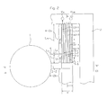
- Fig. 2 which is a partial enlargement of the one-dimensional optical deflector 10A of Fig. 1 , the lengths of the linear piezoelectric actuator 4-2a and the piezoelectric sensor 5 are defined by L 4a and L 5 , respectively.
- L 4 ⁇ a / 6 ⁇ L 5 ⁇ L 4 ⁇ a / 3
- the width of the linear piezoelectric actuators 4-2a and 4-2b and the piezoelectric sensor 5 is representatively defined by W.
- the piezoelectric sensor 5 is divided into five piezoelectric sensor elements 5-1, 5-2, 5-3, 5-4 and 5-5 which are equidistantly arranged along the width direction. That is, the width of each of the piezoelectric sensor elements 5-1, 5-2, 5-3, 5-4 and 5-5 is W/5.
- the piezoelectric sensor element 5-1 is connected via a conductive layer 112-1 over the linear piezoelectric actuator 4-2a to the pad P XS on the rectangular support frame 2, while the piezoelectric sensor elements 5-2, 5-3, 5-4 and 5-5 are connected via conductive layers 112-2, 112-3, 112-4 and 112-5 over the linear piezoelectric actuator 4-2a to the pad P GND on the rectangular support frame 2.
- the Pt upper electrode layers of the piezoelectric sensor elements 5-2, 5-3, 5-4 and 5-5 are grounded, so that the piezoelectric sensor elements 5-2, 5-3, 5-4 and 5-5 are inactivated.
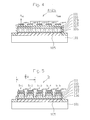
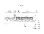
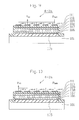
- Figs. 3 , 4 , 5 and 6 which are cross-sectional views of the optical deflector of Fig. 2 taken along the line III-III, the line IV-IV, the line V-V and the line VI-VI, respectively, in Fig. 2 , an about 40 ⁇ m thick silicon "Device” layer 101, an about 2 ⁇ m thick silicon dioxide “Box” layer 102 and an about 400 ⁇ m thick silicon "Handle” layer 103 are formed by using a silicon-on-insulator (SOI) wafer.
- SOI silicon-on-insulator
- silicon dioxide layers 104 and 105 are formed on both surfaces of the SOI wafer.
- an about 50 nm thick Ti (or TiO x ) contact layer 106 is formed on the silicon dioxide layer 105, and an about 150 nm thick Pt lower electrode layer 107 is formed on the contact layer 106. Also, an about 3 ⁇ m thick lead titanate zirconate PbZrTiO 2 (PZT) piezoelectric layer 108 is formed on the Pt lower electrode layer 107. Further, an about 150 nm thick Pt upper electrode layer 109 and an about 50 nm thick Ti contact layer 110 are formed on the PZT layer 108.
- an about 500 nm thick silicon dioxide layer 111 is formed on the Ti contact layer 110 and is patterned to form contact holes in the silicon dioxide layer 111.
- the above-mentioned conductive layers 112-1, 112-2, 112-3, 112-4 and 112-5 and conductive layers (not shown) for the pads P Xa , P Xb , P GND and P S are made of about 500 nm thick Al or Au and are formed in the contact holes of the silicon dioxide layer 111.
- a Ti contact layer 113 and an Ag reflective layer 114 are formed.
- the circular mirror 1 is constructed by the silicon "Device” layers 101, the Ti contact layer 113 and the Ag or Au reflective layer 114.
- the rectangular support frame 2 is constructed by the silicon "Device” layers 101, the silicon dioxide “Box” layer 102, the silicon “Handle” layer 103 and the silicon dioxide layers 104 and 111.
- the torsion bar 3-2 as well as the torsion bar 3-1 are constructed by the silicon "Device” layer 101 and the silicon dioxide layer 111.
- the linear piezoelectric actuator 4-2a as well as the linear piezoelectric actuators 4-1a, 4-1b and 4-2b are constructed by the silicon "Device" layer 101, the silicon dioxide layer 105, the Ti contact layer 106, the Pt lower electrode layer 107, the PZT piezoelectric layer 108, the Pt upper electrode layer 109, the Ti contact layer 110 and the silicon dioxide layer 111.
- the conductive layers 112-1, 112-2, 112-3, 112-4 and 112-5 are not connected to the Pt upper electrode layer 109 of the linear piezoelectric actuator 4-2a.
- the piezoelectric sensor 5 is constructed by the silicon "Device" layer 101, the silicon dioxide layer 105, the Ti contact layer 106, the Pt lower electrode layer 107, the PZT piezoelectric layer 108, the Pt upper electrode layer 109, the Ti contact layer 110, the silicon dioxide layer 111 and the conductive layers 112-1, 112-2, 112-3, 112-4 and 112-5.
- the groove 6 is formed between the linear piezoelectric actuator 4-2a and the piezoelectric sensor 5, so that the PZT piezoelectric layer 108, the Pt upper electrode layer 109 and the Ti contact layer 110 of the linear piezoelectric actuator 4-2a are electrically separated from those of the piezoelectric sensor 5.
- the conductive layers 112-1, 112-2, 112-3, 112-4 and 112-5 are present in the groove 6.
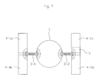
- a stress distribution as illustrated in Fig. 7 was obtained in the one-dimensional optical deflector 10A of Fig. 1 .
- the stronger stress whether it is a compression stress or a tension stress, is shown as darker in the illustration. That is, the strong stress was concentrated at an inner-side portion of the piezoelectric sensor 5 in the vicinity of the torsion bar 3-2. Therefore, the piezoelectric sensor elements 5-1 and 5-2 than the piezoelectric sensor element 5-3, 5-4 and 5-5 are susceptible to the stress generated in the one-dimensional optical deflector 10A of Fig. 1 .
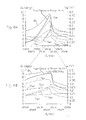
- Fig. 8A depicts a graph showing the relationship between the frequency f x of the sinusoidal-wave drive voltages V Xa and V Xb and the deflection angle ⁇ x of the circular mirror 1 of Fig. 1 and the relationship between the frequency f x and the peak-to-peak voltages V pp1 , V pp2 , V pp3 , V pp4 and V pp5 of the sense voltages of the piezoelectric sensor elements 5-1, 5-2, 5-3, 5-4 and 5-5 where the piezoelectric sensor elements 5-1, 5-2, 5-3, 5-4 and 5-5 are separated from each other, i.e., the conductive layers 112-2, 112-3, 112-4 and 112-5 are not connected to the pad P GND .
- Fig. 8B is a partial enlargement of Fig. 8A .
- the sense voltages at the conductive layers 112-1, 112-2, 112-3, 112-4 and 112-5 are derived by using probes, so that the peak-to-peak voltages V pp thereof can be calculated.
- the deflection angle ⁇ x can be detected by using a one-dimensional position sensitive detector (PSD) which detects a center of the spotlight L reflected from the circular mirror 1.
- PSD position sensitive detector
- the one-dimensional PSD is connected to the control circuit 30; however, the one-dimensional PSD is removed in a usual operation mode.
- the peak-to-peak voltage V pp1 of the sense voltage of the piezoelectric sensor element 5-1 is maximum, i.e., 0.356V.
- the piezoelectric sensor elements 5-1, 5-2, 5-3, 5-4 and 5-5 are combined into a single piezoelectric sensor which is expected to generate a sense voltage with a peak-to-peak voltage V pp0 as shown in Figs. 8A and 8B .
- the peak-to-peak voltage V pp0 would be generated in the above-mentioned second prior art one-dimensional piezoelectric actuator.
- the frequency f x of the sinusoidal-wave drive voltages V Xa and V Xb is 25137 Hz (>f R )
- the peak-to-peak voltage V pp0 is maximum, i.e., 0.450V.
- a resonant state can be realized by the peak-to-peak voltage V pp2 of the sense voltage of the piezoelectric sensor element 5-2.
- the conductive layer 112-2 is connected to the pad P S
- the conductive layers 112-1, 112-3, 112-4 and 112-5 are connected to the pad P GND . Therefore, the piezoelectric sensor element 5-2 can be electrostatically shielded by the piezoelectric sensor elements 5-1 and 5-3 whose Pt upper electrode layers are grounded, thus improving the crosstalk characteristics.
- a resonant state can be realized by both of the peak-to-peak voltages V pp1 and V pp2 of the sense voltages of the piezoelectric sensor elements 5-1 and 5-2.
- the conductive layers 112-1 and 112-2 are connected to the pad P S
- the conductive layers 112-3, 112-4 and 112-5 are connected to the pad P GND .
- the piezoelectric sensor elements 5-1 and 5-2 can be combined into a single piezoelectric sensor element 5-12 with a single conductive layer 112-12.
- Fig. 13 which illustrates another modification of Fig. 5 , the PZT piezoelectric layer 108, the Pt upper electrode layer 109 and the Ti contact layer 110 are removed from the piezoelectric sensor elements 5-2, 5-3, 5-4 and 5-5 of Fig. 5 , to simplify the structure of the one-dimensional optical deflector 10A of Fig. 1 .
- the piezoelectric sensor elements 5-1 and/or 5-2, and 5-12 connected to the pad P XS have a width smaller than two-fifths (2/5) of the width W of the piezoelectric actuator 4-2a, and are arranged at a wide portion within two-fifths (2/5) of the width W from the inner end of the linear piezoelectric actuator 4-2a.
- a one-dimensional optical deflector 10B includes torsion bars 3'-1 and 3'-2 instead of the torsion bars 3-1 and 3-2 of Fig. 1 .
- the torsion bars 3'-1 and 3'-2 are coupled between the outer circumference of the circular mirror 1 and the inner end of the rectangular support frame 2. Since the circular mirror 1 is supported by a six-point support at the rectangular support frame 2, the support of the circular mirror 1 is more stable in the optical deflector 10B of Fig. 14 than in the optical deflector 10A of Fig. 1 .
- Fig. 15 which is a partial enlargement of the one-dimensional optical deflector 10B of Fig. 14 , the piezoelectric sensor element 5-1 is connected via a conductive layer 112'-1 over the torsion bar 3'-2 to the pad P XS on the rectangular support frame 2, while the piezoelectric sensor elements 5-2, 5-3, 5-4 and 5-5 are connected via conductive layers 112'-2, 112'-3, 112'-4 and 112'-5 over the torsion bar 3'-2 to the pad P GND on the rectangular support frame 2.
- the Pt upper electrode layers of the piezoelectric sensor elements 5-2, 5-3, 5-4 and 5-5 are grounded, so that the piezoelectric sensor elements 5-2, 5-3, 5-4 and 5-5 are inactivated.
- Figs. 16 , 17 , 18 and 19 are cross-sectional views of the optical deflector of Fig. 15 taken along the line XVI-XVI, the line XVII-XVII, the line XVIII-XVIII and the line XIX-XIX, respectively, in Fig. 15 .
- the conductive layers 112'-1, 112'-2, 112'-3, 112'-4 and 112'-5 extend over the torsion bar 3'-2 to the rectangular support frame 2. Therefore, since the conductive layers 112'-1, 112'-2, 112'-3, 112'-4 and 112'-5 are not provided on the linear piezoelectric actuator 4-2a which would generate noise relating to the crosstalk, the piezoelectric sensor 5 is hardly subject to the crosstalk.
- the conductive layers 112'-1, 112'-2, 112'-3, 112'-4 and 112'-5 are provided on the linear piezoelectric actuator 4-2a.
- the piezoelectric sensor 5 including the piezoelectric sensor elements 5-1, 5-2, 5-3, 5-4 and 5-5 is the same as that as illustrated in Fig. 5 .
- the conductive layer 112'-3 extends from the piezoelectric sensor 5 to the torsion bar 3'-2.
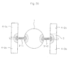
- a stress distribution as illustrated in Fig. 20 was obtained in the one-dimensional optical deflector 10B of Fig. 14 .
- the stronger stress whether it is a compression stress or a tension stress, is shown as darker in the illustration. That is, the stress distribution of Fig. 20 is a little broader that of Fig. 7 .
- the piezoelectric sensor elements 5-1 and 5-2 more than the piezoelectric sensor element 5-3, 5-4 and 5-5 are susceptible to the stress generated in the one-dimensional optical deflector 10B of Fig. 14 .
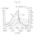
- Fig. 21 depicts a graph showing the relationship between the frequency f x of the sinusoidal-wave drive voltages V Xa and V Xb and the deflection angle ⁇ x of the circular mirror 1 of Fig. 14 and the relationship between the frequency f x and the peak-to-peak voltages V pp1 , V pp2 , V pp3 , V pp4 and V pp5 of the sense voltages of the piezoelectric sensor elements 5-1, 5-2, 5-3, 5-4 and 5-5 where the piezoelectric sensor elements 5-1, 5-2, 5-3, 5-4 and 5-5 are separated from each other, i.e., the conductive layers 112'-2, 112'-3, 112'-4 and 112'-5 are not connected to the pad P GND .
- the sense voltages at the conductive layers 11'2-1, 112'-2, 112'-3, 112'-4 and 112'-5 are derived by using probes, so that the peak-to-peak voltages V pp thereof
- the peak-to-peak voltage V pp1 of the sense voltage of the piezoelectric sensor element 5-1 is maximum, i.e., 0.427V.
- the piezoelectric sensor elements 5-1 and/or 5-2, and 5-12 connected to the pad P XS have a width smaller than two-fifths (2/5) of the width W of the piezoelectric actuator 4-2a, and are arranged at a wide portion within two-fifths (2/5) of the width W from the inner end of the linear piezoelectric actuator 4-2a.
- the mirror 1 can be rectangular or square.
- a one-dimensional optical deflector 10C includes a semi-ring-shaped piezoelectric sensor 4-a with a base coupling portion 7-a coupled to the rectangular support frame 2, instead of the linear piezoelectric actuators 4-1a and 4-2a of Fig. 1 , and also, includes a semi-ring-shaped piezoelectric sensor 4-b with a base coupling portion 7-b coupled to the rectangular support frame 2, instead of the linear piezoelectric actuators 4-1b and 4-2b of Fig. 1 .
- the base coupling portions 7-a and 7-b alternate with the torsion bars 3-1 and 3-2 at 90 degrees.
- the one-dimensional optical deflector 10C includes a curved piezoelectric sensor 5' instead of the piezoelectric sensor 5 of Fig. 1 .
- the circular mirror 1 is supported by a two-point support at the rectangular support frame 2.
- Fig. 23 which is a partial enlargement of the one-dimensional optical deflector 10C of Fig. 22 , the lengths of the semi-ring-shaped piezoelectric actuator 4-a and the curved piezoelectric sensor 5' along their center lines between the base coupling portion 7-a and the torsion bar 7-2 are defined by L' 4a and L' 5 , respectively.
- L ⁇ 4 ⁇ a / 6 L ⁇ 5 ⁇ L ⁇ 4 ⁇ a / 3
- the width of the semi-ring-shaped piezoelectric actuators 4-a and 4-b and the curved piezoelectric sensor 5' is representatively defined by W'.
- the curved piezoelectric sensor 5' is divided into five piezoelectric sensor elements 5'-1, 5'-2, 5'-3, 5'-4 and 5'-5 which are equidistantly arranged along the width direction. That is, the width of each of the piezoelectric sensor elements 5'-1, 5'-2, 5'-3, 5'-4 and 5'-5 is W'/5.
- the piezoelectric sensor element 5'-1 is connected via a conductive layer 112-1 over the semi-ring-shaped piezoelectric actuator 4-a to the pad P XS on the rectangular support frame 2, while the piezoelectric sensor elements 5'-2, 5'-3, 5'-4 and 5'-5 are connected via conductive layers 112-2, 112-3, 112-4 and 112-5 over the semi-ring-shaped piezoelectric actuator 4-a to the pad P GND on the rectangular support frame 2.
- the Pt upper electrode layers of the piezoelectric sensor elements 5'-2, 5'-3, 5'-4 and 5'-5 are grounded, so that the piezoelectric sensor elements 5'-2, 5'-3, 5'-4 and 5'-5 are inactivated.
- conductive layers 112-1, 112-2, 112-3, 112-4 and 112-5 are about the same as those of Figs. 2 , 4 , 6 , 9 , 10 , 11 , 12 and 13 .
- a stress distribution as illustrated in Fig. 24 was obtained in the one-dimensional optical deflector 10C of Fig. 22 .
- the stronger stress whether it is a compression stress or a tension stress, is shown as darker in the illustration. That is, the strong stress was concentrated at an inner-side portion of the curved piezoelectric sensor 5' in the vicinity of the torsion bar 3-2.
- the piezoelectric sensor elements 5'-1 and 5'-2 than the piezoelectric sensor element 5'-3, 5'-4 and 5'-5 are susceptible to the stress generated in the one-dimensional optical deflector 10C of Fig. 22 , in the same way as in the first embodiment.
- the piezoelectric sensor elements 5-1 connected to the pad P XS have a width smaller than two-fifths (2/5) of the width W' of the semi-ring-shaped piezoelectric actuator 4-a, and are arranged at a wide portion within two-fifths (2/5) of the width W' from the inner end of the semi-ring-shaped piezoelectric actuator 4-a.
- a one-dimensional optical deflector 10D includes torsion bars 3'-1 and 3'-2 instead of the torsion bars 3-1 and 3-2 of Fig. 22 .
- the torsion bars 3'-1 and 3'-2 are coupled between the outer circumference of the circular mirror 1 and the inner end of the rectangular support frame 2. Since the circular mirror 1 is supported by a four-point support at the rectangular support frame 2, the support of the circular mirror 1 is more stable in the optical deflector 10D of Fig. 25 than the optical deflector 10C of Fig. 22 .
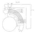
- Fig. 26 which is a partial enlargement of the one-dimensional optical deflector 10D of Fig. 25 , the piezoelectric sensor element 5'-1 is connected via a conductive layer 112'-1 over the torsion bar 3'-2 to the pad P XS on the rectangular support frame 2, while the piezoelectric sensor elements 5'-2, 5'-3, 5'-4 and 5'-5 are connected via conductive layers 112'-2, 112'-3, 112'-4 and 112'-5 over the torsion bar 3'-2 to the pad P GND on the rectangular support frame 2.
- the Pt upper electrode layers of the piezoelectric sensor elements 5'-2, 5'-3, 5'-4 and 5'-5 are grounded, so that the piezoelectric sensor elements 5'-2, 5'-3, 5'-4 and 5'-5 are inactivated.
- conductive layers 112'-1, 112'-2, 112'-3, 112'-4 and 112'-5 are about the same as those of Figs. 15 , 16 , 17, 18 and 19 .
- a stress distribution as illustrated in Fig. 27 was obtained in the one-dimensional optical deflector 10D of Fig. 25 .
- the stronger stress whether it is a compression stress or a tension stress, is shown as darker in the illustration. That is, the stress distribution of Fig. 27 is a little broader that of Fig. 24 .
- the piezoelectric sensor elements 5'-1 and 5'-2 than the piezoelectric sensor element 5'-3, 5'-4 and 5'-5 are susceptible to the stress generated in the one-dimensional optical deflector 10D of Fig. 25 .
- the piezoelectric sensor elements 5'-1 connected to the pad P XS have a width smaller than two-fifths (2/5) of the width W' of the semi-ring-shaped piezoelectric actuator 4-a, and are arranged at a wide portion within two-fifths (2/5) of the width W' from the inner end of the semi-ring-shaped piezoelectric actuator 4-a.
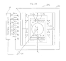
- a one-dimensional optical deflector 10D' includes two piezoelectric sensors 5'a and 5'b which have the same structure as that of the piezoelectric sensor 5' of Fig. 25 .
- the piezoelectric sensors 5'a and 5'b are symmetrical with respect to the center of the optical deflector 10D' of Fig. 28 .
- the semi-ring-shaped piezoelectric actuators 4-a and 4-b are symmetrical with respect to the center of the optical deflector 10D' of Fig. 28 , so that the drive forces (torques) of the semi-ring-shaped piezoelectric actuators 4-a and 4-b are so balanced as to stabilize the operation of the optical deflector 10D'.
- the sense voltages of the piezoelectric sensors 5'a and 5'b are in-phase with each other, a combined sense voltage of the two sense voltages can improve the operation of the optical deflector 10D' of Fig. 28 .
- the operation of the optical deflector 10A, 10B and 10C of Figs. 1 , 14 and 22 can have two piezoelectric sensors in the same way as the optical deflector 10D' of Fig. 28 .
- a two-dimensional optical deflector 10A' includes a movable rectangular support frame 2' instead of the rectangular support frame 2 of Fig. 1 .
- the movable rectangular support frame 2' is constructed by the silicon "Device" layers 101 and the silicon dioxide layer 111 in the same way as the torsion bars 3-1 and 3-2.
- the two-dimensional optical deflector 10A' is further constructed by a rectangular support frame 11 surrounding the movable rectangular support frame 2', a pair of torsion bars 12-1 and 12-2 arranged along the Y-axis coupled to the outer end of the movable rectangular support frame 2', a pair of linear piezoelectric actuators 13-1a and 13-1b arranged between the rectangular support frame 11 and the torsion bar 13-1, a pair of linear piezoelectric actuators 13-2a and 13-2b arranged between the rectangular support frame 11 and the torsion bar 12-2, and a piezoelectric sensor 14 inserted between the torsion bar 12-2 and the linear piezoelectric actuator 13-2a. Also, a groove 15 is provided to separate the piezoelectric sensor 14 from the linear piezoelectric actuator 13-2a.
- movable rectangular support frame 2' is supported by a four-point support at the rectangular support frame 11.
- the linear piezoelectric actuators 13-1a, 13-1b, 13-2a and 13-2b serve as cantilevers for rocking the circular mirror 1 with respect to the Y-axis through the torsion bars 12-1 and 12-2.
- the linear piezoelectric actuator 13-1a opposes the linear piezoelectric actuator 13-1b along the X-axis and sandwich the torsion bar 12-1.
- the flexing direction of the linear piezoelectric actuator 13-1a is opposite to that of the linear piezoelectric actuator 13-1b.
- the linear piezoelectric actuator 13-2a opposes the linear piezoelectric actuator 13-2b along the X-axis and sandwich the torsion bar 12-2.
- the flexing direction of the linear piezoelectric actuator 13-2a is opposite to that of the linear piezoelectric actuator 13-2b. Therefore, the torsion bars 12-1 and 12-2 are twisted by the linear piezoelectric actuators 13-1a, 13-1b, 13-2a and 13-2b to rock the circular mirror 1 with respect to the Y-axis.
- pads P Xa , P Xb , P XS , P Ya , P Yb , P YS and P GND are provided on the rectangular support frame 11 .
- the pads P Ya , P Yb and P YS as well as the pads P Xa , P Xb , P XS are connected to the control circuit 30.
- the control circuit 30 supplies a sinusoidal-wave drive voltage V Ya to the pad P Ya which is connected to the Pt upper electrode layers of the linear piezoelectric actuators 13-1a and 13-2a, thus driving the linear piezoelectric actuators 13-1a and 13-2a.
- the control circuit 30 supplies a sinusoidal-wave drive voltage V Yb opposite in phase to the sinusoidal-wave drive voltage V Ya to the pad P Yb which is connected to the Pt upper electrode layers of the linear piezoelectric actuators 13-1b and 13-2b, thus driving the linear piezoelectric actuators 13-1b and 13-2b.
- control circuit 30 receives a sense voltage V YS from the pad P YS which is connected to the Pt upper electrode layers of the piezoelectric sensor 14, and controls the sinusoidal-wave drive voltages V Ya and V Yb by the feedback of the sense voltage V YS thereto.
- pad P GND is further connected to the Pt lower electrode layers of the linear piezoelectric actuators 13-1a, 13-1b, 13-2a, 13-2b and the piezoelectric sensor 14.
- the frequency f Y of the sinusoidal-wave drive voltages V Ya and V Yb is smaller the frequency f X of the sinusoidal-wave drive voltages V Xa and V Xb .
- the rectangular support frame 11 is constructed by the silicon “Device” layers 101, the silicon dioxide “Box” layer 102, the silicon “Handle” layer 103 and the silicon dioxide layers 104 and 111 in the same way as the rectangular support frame 2 of Fig. 1 .
- the torsion bars 12-1 and 12-2, the linear piezoelectric actuator 13-1a, 13-1b, 13-2a and 13-2b, the piezoelectric sensor 14 and the groove 15 have the same structures as the torsion bars 3-1 and 3-2, the linear piezoelectric actuator 4-1a, 4-1b, 4-2a and 4-2b, the piezoelectric sensor 5 and the groove 6, respectively, of Fig. 1 .
- the piezoelectric sensor 14 has the same structure as the piezoelectric sensor 5 of Fig. 1 . That is, the piezoelectric sensor 14 has one or two piezoelectric sensor elements connected to the pad P XS which have a width smaller than two-fifths (2/5) of the width W of the piezoelectric actuator 13-2a, and are arranged at a wide portion within two-fifths (2/5) of the width W from the inner end of the linear piezoelectric actuator 13-2a.
- Fig. 30 illustrates a two-dimensional optical deflector 10B' which is a modification of the optical deflector 10B of Fig. 14 , torsion bars 12'-1 and 12'-2 and a piezoelectric sensor 14' provided instead of the torsion bars 12-1 and 12-2 and the piezoelectric sensor 14 of Fig. 29 .
- the torsion bars 12'-1 and 12'-2 and coupled between the outer end of the movable rectangular support frame 2' and the inner end of the rectangular support frame 11. Since the movable rectangular support frame 2' is supported by a six-point support at the rectangular support frame 11, the support of the movable rectangular support frame 2' is more stable in the optical deflector 10B' of Fig. 30 than in the optical deflector 10A' of Fig. 29 .
- the piezoelectric sensor 14 has the same structure as the piezoelectric sensor 5 of Fig. 15 . That is, the piezoelectric sensor 14 has one or two piezoelectric sensor elements connected to the pad P XS which have a width smaller than two-fifths (2/5) of the width W of the linear piezoelectric actuator 13-2a, and are arranged at a wide portion within two-fifths (2/5) of the width W from the inner end of the linear piezoelectric actuator 13-2a.
- the one-dimensional optical deflectors 10C, 10D and 10D' of Figs. 22 , 25 and 28 can be modified into two-dimensional optical deflectors, in the same way as the two-dimensional optical deflectors 10A' and 10B' of Figs. 29 and 30 .
- two torsion bars are provided for the X-axis of the mirror 1: however, a single torsion bar can be provided for the X-axis of the mirror 1. Also, in the above-described modifications as illustrated in Figs. 29 and 30 , two torsion bars are provided for the Y-axis of the mirror 1; however, a single torsion bar can be provided for the Y-axis of the mirror 1.
Landscapes
- Physics & Mathematics (AREA)
- General Physics & Mathematics (AREA)
- Optics & Photonics (AREA)
- Mechanical Light Control Or Optical Switches (AREA)
- Micromachines (AREA)
- Mechanical Optical Scanning Systems (AREA)
- Facsimile Scanning Arrangements (AREA)
Abstract
Description
- This application claims the priority benefit under 35 U.S.C. §119 to Japanese Patent Application No.
JP2012-199364 filed on September 11, 2012 - The presently disclosed subject matter relates to an optical deflector used as a scanner in a projector, a bar code reader, a laser printer, a laser read amplifier, a head-up display apparatus or the like.
- Recently, in a projector or the like, a spotlight is deflected by an optical deflector and then, is projected on a screen. Such an optical deflector is a micro electro mechanical system (MEMS) device manufactured by semiconductor manufacturing processes and micro machine technology.
- A first prior art one-dimensional optical deflector is constructed by a circular mirror, a support frame surrounding the circular mirror, a pair of torsion bars connected between the support frame and the circular mirror, piezoelectric actuators provided between the support frame and the torsion bars for vibrating (rocking) the circular mirror through the torsion bars with respect to an axis of the circular mirror, and two semi-ring-shaped piezoelectric sensors provided at a circumference of the circular mirror for sensing rocking vibrations caused by the piezoelectric actuators (see:
Fig. 1 ofJP2011-150055 - The above-described first prior art one-dimensional optical deflector has, however, the following problems:
- a) Since the semi-ring-shaped piezoelectric actuators are also rocked in association with rocking of the mirror, the resonant frequency thereof would be decreased.
- b) Since conductive layers located from the semi-ring-shaped piezoelectric sensors on the circular mirror through the torsion bars to pads on the support frame are very long, the resonant frequency of the circular mirror is also affected by the weight of the conductive layers, so that the resonant frequency of the circular mirror would fluctuate from an optimum design value.
- c) When one of the semi-ring-shaped piezoelectric sensors is expanded, and the other semi-ring-shaped piezoelectric sensor is retracted, the sense voltages of the two semi-ring-shaped piezoelectric sensors opposite in phase to each other would be compensated for by each other, thus reducing the entire detected sense voltages of the semi-ring-shaped piezoelectric sensors.
- In a second prior art one-dimensional optical deflector, one piezoelectric sensor is provided between one of the torsion bars and one of the piezoelectric actuators on the same beam as that of the one of the piezoelectric actuators, thus solving all the problems of the above-described first prior art one-dimensional optical deflector (see:
Figs. 16 ,17 and 18 ofJP2010-197994A US2010/0195180A1 ). - In the above-described second prior art one-dimensional optical deflector, however, since the width of the piezoelectric sensor is the same as that of the piezoelectric actuators, the accuracy of the sense voltage of the piezoelectric sensor with respect to a resonant frequency is insufficient. As a result, even when the frequency of sinusoidal-wave drive voltages for the piezoelectric actuators is controlled by the sense voltage of the piezoelectric sensor, a resonant state cannot be realized. This will be discussed in detail later.
- Note that, if a resonant state cannot be realized, it would be required to increase the drive voltages for the piezoelectric actuators in order to obtain a desired deflection angle of the circular mirror.
- The presently disclosed subject matter seeks to solve one or more of the above-described problems.
- According to the presently disclosed subject matter, in an optical deflector including a mirror, a support frame surrounding the mirror, at least one torsion bar arranged along an axis of the mirror having an end coupled to an outer circumference of the mirror, a pair of piezoelectric actuators arranged between the support frame and the torsion bar, and a piezoelectric sensor inserted between the torsion bar and one of the piezoelectric actuators, the piezoelectric sensor includes at least one piezoelectric sensor element the width thereof being smaller than two-fifths of the width of the one of the piezoelectric actuators and being arranged at a wide portion within two-fifths of the width from an inner end of the one of the piezoelectric actuators.
- According to the presently disclosed subject matter, since the piezoelectric sensor element is narrow, within two-fifths of the width from an inner end of the one of the piezoelectric actuators, a resonant state can be realized by the feedback control of a sense voltage of the piezoelectric sensor element to drive voltages of the piezoelectric actuators.
- The above and other advantages and features of the presently disclosed subject matter will be more apparent from the following description of certain embodiments, taken in conjunction with the accompanying drawings, wherein:
-
Fig. 1 is a plan view illustrating a first embodiment of the optical deflector according to the presently disclosed subject matter; -
Fig. 2 is a partial enlargement of the optical deflector ofFig. 1 ; -
Fig. 3 is a cross-sectional view of the optical deflector taken along the line III-III inFig. 2 ; -
Fig. 4 is a cross-sectional view of the optical deflector taken along the line IV-IV inFig. 2 ; -
Fig. 5 is a cross-sectional view of the optical deflector taken along the line V-V inFig. 2 ; -
Fig. 6 is a cross-sectional view of the optical deflector taken along the line VI-VI inFig. 2 ; -
Fig. 7 is a diagram illustrating a simulated stress distribution in the optical deflector ofFig. 1 ; -
Fig. 8A is a graph showing the relationship between the frequency of sinusoidal-wave drive voltages and the deflection angle of the circular mirror ofFig. 1 and the relationship between the frequency of sinusoidal-wave drive voltages and the peak-to-peak voltages of the sense voltages of the piezoelectric sensor elements of the piezoelectric sensor ofFig. 1 ; -
Fig. 8B is a partial enlargement ofFig. 8A ; -
Fig. 9 is a cross-sectional view illustrating a modification ofFig. 4 ; -
Fig. 10 is a cross-sectional view illustrating another modification ofFig. 4 ; -
Fig. 11 is a cross-sectional view illustrating a further modification ofFig. 4 ; -
Fig. 12 is a cross-sectional view illustrating a modification ofFig. 5 ; -
Fig. 13 is a cross-sectional view illustrating another modification ofFig. 5 ; -
Fig. 14 is a plan view illustrating a second embodiment of the optical deflector according to the presently disclosed subject matter; -
Fig. 15 is a partial enlargement of the optical deflector ofFig. 14 ; -
Fig. 16 is a cross-sectional view of the optical deflector taken along the line XVI-XVI inFig. 15 ; -
Fig. 17 is a cross-sectional view of the optical deflector taken along the line XVII-XVII inFig. 15 ; -
Fig. 18 is a cross-sectional view of the optical deflector taken along the line XVIII-XVIII inFig. 15 ; -
Fig. 19 is a cross-sectional view of the optical deflector taken along the line XIX-XIX inFig. 15 ; -
Fig. 20 is a diagram illustrating a simulated stress distribution in the optical deflector ofFig. 14 ; -
Fig. 21 is a graph showing the relationship between the frequency of sinusoidal-wave drive voltages and the deflection angle of the circular mirror ofFig. 14 and the relationship between the frequency of sinusoidal-wave drive voltages and the peak-to-peak voltages of the sense voltages of the piezoelectric sensor elements of the piezoelectric sensor ofFig. 14 ; -
Fig. 22 is a plan view illustrating a third embodiment of the optical deflector according to the presently disclosed subject matter; -
Fig. 23 is a partial enlargement of the optical deflector ofFig. 22 ; -
Fig. 24 is a diagram illustrating a simulated stress distribution in the optical deflector ofFig. 22 ; -
Fig. 25 is a plan view illustrating a fourth embodiment of the optical deflector according to the presently disclosed subject matter; -
Fig. 26 is a partial enlargement of the optical deflector ofFig. 25 ; -
Fig. 27 is a diagram illustrating a simulated stress distribution in the optical deflector ofFig. 25 ; -
Fig. 28 is a plan view illustrating a modification of the optical deflector ofFig. 22 ; -
Fig. 29 is a plan view illustrating a modification of the optical deflector ofFig. 1 ; and -
Fig. 30 is a plan view illustrating a modification of the optical deflector ofFig. 14 . - In
Fig. 1 , which illustrates a first embodiment of the optical deflector according to the presently disclosed subject matter, a one-dimensionaloptical deflector 10A is constructed by acircular mirror 1 for reflecting a spotlight L from alaser diode 20, arectangular support frame 2 surrounding thecircular mirror 1, a pair of torsion bars 3-1 and 3-2 arranged along an X-axis of thecircular mirror 1 coupled to the outer circumference of thecircular mirror 1, a pair of linear piezoelectric actuators 4-1a and 4-1b arranged between therectangular support frame 2 and the torsion bar 3-1, a pair of linear piezoelectric actuators 4-2a and 4-2b arranged between therectangular support frame 2 and the torsion bar 3-2, and apiezoelectric sensor 5 inserted between the torsion bar 3-2 and the linear piezoelectric actuator 4-2a. Also, agroove 6 is provided to separate thepiezoelectric sensor 5 from the linear piezoelectric actuator 4-2a. - In
Fig. 1 , thecircular mirror 1 is supported by a four-point support at therectangular support frame 2. - The linear piezoelectric actuators 4-1a, 4-1b, 4-2a and 4-2b serve as cantilevers for rocking the
circular mirror 1 with respect to the X-axis through the torsion bars 3-1 and 3-2. - In more detail, the linear piezoelectric actuator 4-1a opposes the linear piezoelectric actuator 4-1b along the Y-axis of the
circular mirror 1 perpendicular to the X-axis thereof and sandwich the torsion bar 3-1. In this case, the flexing direction of the linear piezoelectric actuator 4-1a is opposite to that of the linear piezoelectric actuator 4-1b. Similarly, the linear piezoelectric actuator 4-2a opposes the linear piezoelectric actuator 4-2b along the Y-axis and sandwich the torsion bar 3-2. In this case, the flexing direction of the linear piezoelectric actuator 4-2a is opposite to that of the linear piezoelectric actuator 4-2b. Therefore, the torsion bars 3-1 and 3-2 are twisted by the linear piezoelectric actuators 4-1a, 4-1b, 4-2a and 4-2b to rock thecircular mirror 1 with respect to the X-axis. - Provided on the
rectangular support frame 2 are pads PXa, PXb, PXS and PGND. The pads PXa, PXb and PXS are connected to acontrol circuit 30 which is constructed by a microcomputer or the like, while the pad PGND is grounded. - The
control circuit 30 supplies a sinusoidal-wave drive voltage VXa to the pad PXa which is connected to the Pt upper electrode layer 109 (shown not inFig. 1 , but inFigs. 4 ,6 ,9, 10 and11 ) of the linear piezoelectric actuators 4-1a and 4-2a, thus driving the linear piezoelectric actuators 4-1a and 4-2a. On the other hand, thecontrol circuit 30 supplies a sinusoidal-wave drive voltage VXb opposite in phase to the sinusoidal-wave drive voltage VXa to the pad PXb which is connected to the Pt upper electrode layer 109 (shown not inFig. 2 , but inFigs. 4 ,6 ,9, 10 and11 ) of the linear piezoelectric actuators 4-1b and 4-2b, thus driving the linear piezoelectric actuators 4-1b and 4-2b. - Also, the
control circuit 30 receives a sense voltage VXS from the pad PXS which is connected to the Pt upper electrode layer 109 (shown not inFig. 2 , but inFigs. 5 ,6 and12 ) of thepiezoelectric sensor 5, and controls the sinusoidal-wave drive voltages VXa and VXb by the feedback of the sense voltage VXS thereto. - Note that the pad PGND is connected to the lower electrode layer 107 (shown not in
Fig. 1 , but inFigs. 4, 5 ,6 ,9, 10 ,11, 12 and13 ) of the linear piezoelectric actuators 4-1a, 4-1b, 4-2a, 4-2b and thepiezoelectric sensor 5. - Further, the
control circuit 30 controls thelaser diode 20 to turn ON and OFF the spotlight L. As occasion demands, thecontrol circuit 30 may adjust thelaser diode 20 to change the light amount of the spotlight L. - In
Fig. 2 , which is a partial enlargement of the one-dimensionaloptical deflector 10A ofFig. 1 , the lengths of the linear piezoelectric actuator 4-2a and thepiezoelectric sensor 5 are defined by L4a and L5, respectively. In this case,
- Note that the length Lg of the
groove 6 is very small and can be negligible. - When L5 ≦ L4a/6, the sense voltage VXS of the
piezoelectric sensor 5 is too small. On the other hand, when L5 ≧ L4a/3, the drive force of the piezoelectric actuator 4-2a is too small. - Also, the width of the linear piezoelectric actuators 4-2a and 4-2b and the
piezoelectric sensor 5 is representatively defined by W. - The
piezoelectric sensor 5 is divided into five piezoelectric sensor elements 5-1, 5-2, 5-3, 5-4 and 5-5 which are equidistantly arranged along the width direction. That is, the width of each of the piezoelectric sensor elements 5-1, 5-2, 5-3, 5-4 and 5-5 is W/5. The piezoelectric sensor element 5-1 is connected via a conductive layer 112-1 over the linear piezoelectric actuator 4-2a to the pad PXS on therectangular support frame 2, while the piezoelectric sensor elements 5-2, 5-3, 5-4 and 5-5 are connected via conductive layers 112-2, 112-3, 112-4 and 112-5 over the linear piezoelectric actuator 4-2a to the pad PGND on therectangular support frame 2. In other words, the Pt upper electrode layers of the piezoelectric sensor elements 5-2, 5-3, 5-4 and 5-5 are grounded, so that the piezoelectric sensor elements 5-2, 5-3, 5-4 and 5-5 are inactivated. - In
Figs. 3 ,4 ,5 and6 , which are cross-sectional views of the optical deflector ofFig. 2 taken along the line III-III, the line IV-IV, the line V-V and the line VI-VI, respectively, inFig. 2 , an about 40 µ m thick silicon "Device"layer 101, an about 2 µ m thick silicon dioxide "Box"layer 102 and an about 400 µ m thick silicon "Handle"layer 103 are formed by using a silicon-on-insulator (SOI) wafer. - Also, about 500 nm thick silicon dioxide layers 104 and 105 are formed on both surfaces of the SOI wafer.
- Further, an about 50 nm thick Ti (or TiOx)
contact layer 106 is formed on thesilicon dioxide layer 105, and an about 150 nm thick Ptlower electrode layer 107 is formed on thecontact layer 106. Also, an about 3 µ m thick lead titanate zirconate PbZrTiO2 (PZT)piezoelectric layer 108 is formed on the Ptlower electrode layer 107. Further, an about 150 nm thick Ptupper electrode layer 109 and an about 50 nm thickTi contact layer 110 are formed on thePZT layer 108. - Still further, an about 500 nm thick
silicon dioxide layer 111 is formed on theTi contact layer 110 and is patterned to form contact holes in thesilicon dioxide layer 111. The above-mentioned conductive layers 112-1, 112-2, 112-3, 112-4 and 112-5 and conductive layers (not shown) for the pads PXa, PXb, PGND and PS are made of about 500 nm thick Al or Au and are formed in the contact holes of thesilicon dioxide layer 111. - Furthermore, a
Ti contact layer 113 and an Agreflective layer 114 are formed. - As illustrated in
Fig. 3 , thecircular mirror 1 is constructed by the silicon "Device" layers 101, theTi contact layer 113 and the Ag or Aureflective layer 114. - As illustrated in
Fig. 3 , therectangular support frame 2 is constructed by the silicon "Device" layers 101, the silicon dioxide "Box"layer 102, the silicon "Handle"layer 103 and the silicon dioxide layers 104 and 111. - As illustrated in
Fig. 3 , the torsion bar 3-2 as well as the torsion bar 3-1 are constructed by the silicon "Device"layer 101 and thesilicon dioxide layer 111. - As illustrated in
Figs. 4 and6 , the linear piezoelectric actuator 4-2a as well as the linear piezoelectric actuators 4-1a, 4-1b and 4-2b are constructed by the silicon "Device"layer 101, thesilicon dioxide layer 105, theTi contact layer 106, the Ptlower electrode layer 107, the PZTpiezoelectric layer 108, the Ptupper electrode layer 109, theTi contact layer 110 and thesilicon dioxide layer 111. Note that the conductive layers 112-1, 112-2, 112-3, 112-4 and 112-5 are not connected to the Ptupper electrode layer 109 of the linear piezoelectric actuator 4-2a. - As illustrated in
Figs. 5 and6 , thepiezoelectric sensor 5 is constructed by the silicon "Device"layer 101, thesilicon dioxide layer 105, theTi contact layer 106, the Ptlower electrode layer 107, the PZTpiezoelectric layer 108, the Ptupper electrode layer 109, theTi contact layer 110, thesilicon dioxide layer 111 and the conductive layers 112-1, 112-2, 112-3, 112-4 and 112-5. - Also, in
Fig. 6 , thegroove 6 is formed between the linear piezoelectric actuator 4-2a and thepiezoelectric sensor 5, so that the PZTpiezoelectric layer 108, the Ptupper electrode layer 109 and theTi contact layer 110 of the linear piezoelectric actuator 4-2a are electrically separated from those of thepiezoelectric sensor 5. However, the conductive layers 112-1, 112-2, 112-3, 112-4 and 112-5 are present in thegroove 6. - When a simulation using the Oofelie-Multiphysics V4.4 (trademark) simulation software provided by Open Engineering was performed upon the one-dimensional
optical deflector 10A ofFig. 1 , a stress distribution as illustrated inFig. 7 was obtained in the one-dimensionaloptical deflector 10A ofFig. 1 . InFig. 7 , the stronger stress, whether it is a compression stress or a tension stress, is shown as darker in the illustration. That is, the strong stress was concentrated at an inner-side portion of thepiezoelectric sensor 5 in the vicinity of the torsion bar 3-2. Therefore, the piezoelectric sensor elements 5-1 and 5-2 than the piezoelectric sensor element 5-3, 5-4 and 5-5 are susceptible to the stress generated in the one-dimensionaloptical deflector 10A ofFig. 1 . -
Fig. 8A depicts a graph showing the relationship between the frequency fx of the sinusoidal-wave drive voltages VXa and VXb and the deflection angle θ x of thecircular mirror 1 ofFig. 1 and the relationship between the frequency fx and the peak-to-peak voltages Vpp1, Vpp2, Vpp3, Vpp4 and Vpp5 of the sense voltages of the piezoelectric sensor elements 5-1, 5-2, 5-3, 5-4 and 5-5 where the piezoelectric sensor elements 5-1, 5-2, 5-3, 5-4 and 5-5 are separated from each other, i.e., the conductive layers 112-2, 112-3, 112-4 and 112-5 are not connected to the pad PGND. Also,Fig. 8B is a partial enlargement ofFig. 8A . The sense voltages at the conductive layers 112-1, 112-2, 112-3, 112-4 and 112-5 are derived by using probes, so that the peak-to-peak voltages Vpp thereof can be calculated. - Note that the deflection angle θ x can be detected by using a one-dimensional position sensitive detector (PSD) which detects a center of the spotlight L reflected from the
circular mirror 1. The one-dimensional PSD is connected to thecontrol circuit 30; however, the one-dimensional PSD is removed in a usual operation mode. - As shown in
Figs. 8A and 8B , when the frequency fx of the sinusoidal-wave drive voltages VXa and VXb is 25134 Hz, the deflection angle θx of thecircular mirror 1 is maximum. Therefore, 25134 Hz is a resonant frequency fR, i.e., fR=25134 Hz. - Also, as shown in
Figs. 8A and 8B , when the frequency fx of the sinusoidal-wave drive voltages VXa and VXb is 25134 Hz (=fR), the peak-to-peak voltage Vpp1 of the sense voltage of the piezoelectric sensor element 5-1 is maximum, i.e., 0.356V. In this case, the noise level at a frequency 20032 Hz of the sinusoidal-wave drive voltages VXa and VXb is 0.0374V, and therefore, the signal-to-noise (S/N) ratio is 9.5 (=0.356/0.0374) which is sufficiently high. Therefore, when the frequency fx of the sinusoidal-wave drive voltages VXa and VXb is controlled by the feedback of the peak-to-peak voltage Vpp1 of the sense voltage of the piezoelectric sensor element 5-1 thereto, so that the peak-to-peak voltage Vpp1 is brought close to its maximum value 0.356V, a resonant state (fx=fR) can be realized. - Further, as shown in
Figs. 8A and 8B , when the frequency fx of the sinusoidal-wave drive voltages VXa and VXb is 25134 Hz (=fR), the peak-to-peak voltage Vpp2 of the sense voltage of the piezoelectric sensor element 5-2 is maximum, i.e., 0.235V. In this case, the S/N ratio is a little low. However, when the frequency fx of the sinusoidal-wave drive voltages VXa and VXb is controlled by the feedback of the peak-to-peak voltage Vpp2 of the sense voltage of the piezoelectric sensor element 5-2 thereto, so that the peak-to-peak voltage Vpp2 is brought close to its maximum value 0.235V, a resonant state (fx=fR) can be realized. - On the other hand, as shown in
Figs. 8A and 8B , when the frequency fx of the sinusoidal-wave drive voltages VXa and VXb is 25138 Hz (>fR), the peak-to-peak voltage Vpp3 of the sense voltage of the piezoelectric sensor element 5-3 is maximum, i.e., 0.250V. Therefore, even when the frequency fx of the sinusoidal-wave drive voltages VXa and VXb is controlled by the feedback of the peak-to-peak voltage Vpp3 of the sense voltage of the piezoelectric sensor element 5-3 thereto, so that the peak-to-peak voltage Vpp3 is brought close to its maximum value 0.250V, a resonant state (fx=fR) cannot be realized. - Also, as shown in
Figs. 8A and 8B , when the frequency fx of the sinusoidal-wave drive voltages VXa and VXb is 25138 Hz (>fR), the peak-to-peak voltage Vpp4 of the sense voltage of the piezoelectric sensor element 5-4 is maximum, i.e., 0.270V. Therefore, even when the frequency fx of the sinusoidal-wave drive voltages VXa and VXb is controlled by the feedback of the peak-to-peak voltage Vpp4 of the sense voltage of the piezoelectric sensor element 5-4 thereto, so that the peak-to-peak voltage Vpp4 is brought close to its maximum value 0.270V, a resonant state (fx=fR) cannot be realized. - Further, as shown in
Figs. 8A and 8B , when the frequency fx of the sinusoidal-wave drive voltages VXa and VXb is 25140 Hz (>fR), the peak-to-peak voltage Vpp5 of the sense voltage of the piezoelectric sensor element 5-5 is maximum, i.e., 0.141V. Therefore, even when the frequency fx of the sinusoidal-wave drive voltages VXa and VXb is controlled by the feedback of the peak-to-peak voltage Vpp5 of the sense voltage of the piezoelectric sensor element 5-5 thereto, so that the peak-to-peak voltage Vpp5 is brought close to its maximum value 0.141V, a resonant state (fx=fR) cannot be realized. - If the piezoelectric sensor elements 5-1, 5-2, 5-3, 5-4 and 5-5 are combined into a single piezoelectric sensor which is expected to generate a sense voltage with a peak-to-peak voltage Vpp0 as shown in
Figs. 8A and 8B . Note that the peak-to-peak voltage Vpp0 would be generated in the above-mentioned second prior art one-dimensional piezoelectric actuator. When the frequency fx of the sinusoidal-wave drive voltages VXa and VXb is 25137 Hz (>fR), the peak-to-peak voltage Vpp0 is maximum, i.e., 0.450V. Therefore, even when the frequency fx of the sinusoidal-wave drive voltages VXa and VXb is controlled by the feedback of the peak-to-peak voltage Vpp0 of the sense voltage of the single piezoelectric sensor thereto, so that the peak-to-peak voltage Vpp0 is brought close to its maximum value 0.450V, a resonant state cannot be realized. - As explained above, a resonant state can be realized by the peak-to-peak voltage Vpp2 of the sense voltage of the piezoelectric sensor element 5-2. In this case, as illustrated in
Fig. 9 , the conductive layer 112-2 is connected to the pad PS, while the conductive layers 112-1, 112-3, 112-4 and 112-5 are connected to the pad PGND. Therefore, the piezoelectric sensor element 5-2 can be electrostatically shielded by the piezoelectric sensor elements 5-1 and 5-3 whose Pt upper electrode layers are grounded, thus improving the crosstalk characteristics. - Also, a resonant state can be realized by both of the peak-to-peak voltages Vpp1 and Vpp2 of the sense voltages of the piezoelectric sensor elements 5-1 and 5-2. In this case, as illustrated in
Fig. 10 , the conductive layers 112-1 and 112-2 are connected to the pad PS, while the conductive layers 112-3, 112-4 and 112-5 are connected to the pad PGND. However, as illustrated inFigs. 11 and 12 , the piezoelectric sensor elements 5-1 and 5-2 can be combined into a single piezoelectric sensor element 5-12 with a single conductive layer 112-12. - In
Fig. 13 , which illustrates another modification ofFig. 5 , the PZTpiezoelectric layer 108, the Ptupper electrode layer 109 and theTi contact layer 110 are removed from the piezoelectric sensor elements 5-2, 5-3, 5-4 and 5-5 ofFig. 5 , to simplify the structure of the one-dimensionaloptical deflector 10A ofFig. 1 . - As illustrated in
Figs. 5 ,12 and13 , the piezoelectric sensor elements 5-1 and/or 5-2, and 5-12 connected to the pad PXS have a width smaller than two-fifths (2/5) of the width W of the piezoelectric actuator 4-2a, and are arranged at a wide portion within two-fifths (2/5) of the width W from the inner end of the linear piezoelectric actuator 4-2a. - In
Fig. 14 , which illustrates a second embodiment of the optical deflector according to the presently disclosed subject matter, a one-dimensionaloptical deflector 10B includes torsion bars 3'-1 and 3'-2 instead of the torsion bars 3-1 and 3-2 ofFig. 1 . The torsion bars 3'-1 and 3'-2 are coupled between the outer circumference of thecircular mirror 1 and the inner end of therectangular support frame 2. Since thecircular mirror 1 is supported by a six-point support at therectangular support frame 2, the support of thecircular mirror 1 is more stable in theoptical deflector 10B ofFig. 14 than in theoptical deflector 10A ofFig. 1 . - In
Fig. 15 , which is a partial enlargement of the one-dimensionaloptical deflector 10B ofFig. 14 , the piezoelectric sensor element 5-1 is connected via a conductive layer 112'-1 over the torsion bar 3'-2 to the pad PXS on therectangular support frame 2, while the piezoelectric sensor elements 5-2, 5-3, 5-4 and 5-5 are connected via conductive layers 112'-2, 112'-3, 112'-4 and 112'-5 over the torsion bar 3'-2 to the pad PGND on therectangular support frame 2. In other words, the Pt upper electrode layers of the piezoelectric sensor elements 5-2, 5-3, 5-4 and 5-5 are grounded, so that the piezoelectric sensor elements 5-2, 5-3, 5-4 and 5-5 are inactivated. -
Figs. 16 ,17 ,18 and19 are cross-sectional views of the optical deflector ofFig. 15 taken along the line XVI-XVI, the line XVII-XVII, the line XVIII-XVIII and the line XIX-XIX, respectively, inFig. 15 . - As illustrated in
Figs. 15 and16 , the conductive layers 112'-1, 112'-2, 112'-3, 112'-4 and 112'-5 extend over the torsion bar 3'-2 to therectangular support frame 2. Therefore, since the conductive layers 112'-1, 112'-2, 112'-3, 112'-4 and 112'-5 are not provided on the linear piezoelectric actuator 4-2a which would generate noise relating to the crosstalk, thepiezoelectric sensor 5 is hardly subject to the crosstalk. - As illustrated in
Figs. 15 and17 , the conductive layers 112'-1, 112'-2, 112'-3, 112'-4 and 112'-5 are provided on the linear piezoelectric actuator 4-2a. - As illustrated in
Fig. 18 , thepiezoelectric sensor 5 including the piezoelectric sensor elements 5-1, 5-2, 5-3, 5-4 and 5-5 is the same as that as illustrated inFig. 5 . - As illustrated in
Fig. 19 , the conductive layer 112'-3 extends from thepiezoelectric sensor 5 to the torsion bar 3'-2. - When a simulation using Oofelie-Multiphysics V4.4 (trademark) simulation software provided by Open Engineering was performed upon the one-dimensional
optical deflector 10B ofFig. 14 , a stress distribution as illustrated inFig. 20 was obtained in the one-dimensionaloptical deflector 10B ofFig. 14 . InFig. 20 , the stronger stress, whether it is a compression stress or a tension stress, is shown as darker in the illustration. That is, the stress distribution ofFig. 20 is a little broader that ofFig. 7 . Even in this case, the piezoelectric sensor elements 5-1 and 5-2 more than the piezoelectric sensor element 5-3, 5-4 and 5-5 are susceptible to the stress generated in the one-dimensionaloptical deflector 10B ofFig. 14 . -
Fig. 21 depicts a graph showing the relationship between the frequency fx of the sinusoidal-wave drive voltages VXa and VXb and the deflection angle θ x of thecircular mirror 1 ofFig. 14 and the relationship between the frequency fx and the peak-to-peak voltages Vpp1, Vpp2, Vpp3, Vpp4 and Vpp5 of the sense voltages of the piezoelectric sensor elements 5-1, 5-2, 5-3, 5-4 and 5-5 where the piezoelectric sensor elements 5-1, 5-2, 5-3, 5-4 and 5-5 are separated from each other, i.e., the conductive layers 112'-2, 112'-3, 112'-4 and 112'-5 are not connected to the pad PGND. The sense voltages at the conductive layers 11'2-1, 112'-2, 112'-3, 112'-4 and 112'-5 are derived by using probes, so that the peak-to-peak voltages Vpp thereof can be calculated. - As shown in
Fig. 21 , when the frequency fx of the sinusoidal-wave drive voltages VXa and VXb is 25134 Hz, the deflection angle θ x of thecircular mirror 1 is maximum. Therefore, 25134 Hz is a resonant frequency fR, i.e., fR=25134 Hz. - Also, as shown in
Fig. 21 , when the frequency fx of the sinusoidal-wave drive voltages VXa and VXb is 25134 Hz (=fR), the peak-to-peak voltage Vpp1 of the sense voltage of the piezoelectric sensor element 5-1 is maximum, i.e., 0.427V. In this case, the noise level at a frequency 20032 Hz is 0.0440V, and therefore, the S/N ratio is 9. 7 (=0.427/0.0440) which is higher than the S/N ratio 9.5 in theoptical deflector 10A ofFig. 2 . This is because the conductive layers 112'-1, 112'-2, 112'-3, 112'-4 and 112'-5 are shorter than the conductive layers 112-1, 112-2, 112-3, 112-4 and 112-5 ofFig. 2 and the stress distribution ofFig. 20 is broader than that ofFig. 7 due to the six-point support of thecircular mirror 1. Therefore, when the frequency fx of the sinusoidal-wave drive voltages VXa and VXb is controlled by the feedback of the peak-to-peak voltage Vpp1 of the sense voltage of the piezoelectric sensor element 5-1 thereto, so that the peak-to-peak voltage Vpp1 is brought close to its maximum value 0.427V, a resonant state (fx=fR) can be realized. - Other peak-to-peak voltages Vpp2, Vpp3, Vpp4 and Vpp5 of
Fig. 21 are similar to those ofFigs. 8A and Fig. 8B ; however, the other peak-to-peak voltages Vpp2, Vpp3, Vpp4 and Vpp5 ofFig. 21 are a little higher than those ofFigs. 8A and 8B . - The modifications as illustrated in
Figs. 9, 10 ,11, 12 and13 can be applied to theoptical deflector 10B ofFig. 14 . - As illustrated in
Fig. 18 , the piezoelectric sensor elements 5-1 and/or 5-2, and 5-12 connected to the pad PXS have a width smaller than two-fifths (2/5) of the width W of the piezoelectric actuator 4-2a, and are arranged at a wide portion within two-fifths (2/5) of the width W from the inner end of the linear piezoelectric actuator 4-2a. - In the above-described first and second embodiments, the
mirror 1 can be rectangular or square. - In
Fig. 22 , which illustrates a third embodiment of the optical deflector according to the presently disclosed subject matter, a one-dimensionaloptical deflector 10C includes a semi-ring-shaped piezoelectric sensor 4-a with a base coupling portion 7-a coupled to therectangular support frame 2, instead of the linear piezoelectric actuators 4-1a and 4-2a ofFig. 1 , and also, includes a semi-ring-shaped piezoelectric sensor 4-b with a base coupling portion 7-b coupled to therectangular support frame 2, instead of the linear piezoelectric actuators 4-1b and 4-2b ofFig. 1 . The base coupling portions 7-a and 7-b alternate with the torsion bars 3-1 and 3-2 at 90 degrees. Also, the one-dimensionaloptical deflector 10C includes a curved piezoelectric sensor 5' instead of thepiezoelectric sensor 5 ofFig. 1 . - In
Fig. 22 , thecircular mirror 1 is supported by a two-point support at therectangular support frame 2. - In
Fig. 23 , which is a partial enlargement of the one-dimensionaloptical deflector 10C ofFig. 22 , the lengths of the semi-ring-shaped piezoelectric actuator 4-a and the curved piezoelectric sensor 5' along their center lines between the base coupling portion 7-a and the torsion bar 7-2 are defined by L'4a and L'5, respectively. In this case,
- When L'5 ≦ L'4a/6, the sense voltage VXS of the curved piezoelectric sensor 5' is too small. On the other hand, when L'5 ≧ L'4a/3, the drive force of the semi-ring-shaped piezoelectric actuator 4-a is too small.
- Also, the width of the semi-ring-shaped piezoelectric actuators 4-a and 4-b and the curved piezoelectric sensor 5' is representatively defined by W'.
- The curved piezoelectric sensor 5' is divided into five piezoelectric sensor elements 5'-1, 5'-2, 5'-3, 5'-4 and 5'-5 which are equidistantly arranged along the width direction. That is, the width of each of the piezoelectric sensor elements 5'-1, 5'-2, 5'-3, 5'-4 and 5'-5 is W'/5. The piezoelectric sensor element 5'-1 is connected via a conductive layer 112-1 over the semi-ring-shaped piezoelectric actuator 4-a to the pad PXS on the
rectangular support frame 2, while the piezoelectric sensor elements 5'-2, 5'-3, 5'-4 and 5'-5 are connected via conductive layers 112-2, 112-3, 112-4 and 112-5 over the semi-ring-shaped piezoelectric actuator 4-a to the pad PGND on therectangular support frame 2. In other words, the Pt upper electrode layers of the piezoelectric sensor elements 5'-2, 5'-3, 5'-4 and 5'-5 are grounded, so that the piezoelectric sensor elements 5'-2, 5'-3, 5'-4 and 5'-5 are inactivated. - Note that the conductive layers 112-1, 112-2, 112-3, 112-4 and 112-5 are about the same as those of
Figs. 2 ,4 ,6 ,9 ,10 ,11 ,12 and13 . - When a simulation using the Oofelie-Multiphysics V4.4 (trademark) simulation software provided by Open Engineering was performed upon the one-dimensional
optical deflector 10C ofFig. 22 , a stress distribution as illustrated inFig. 24 was obtained in the one-dimensionaloptical deflector 10C ofFig. 22 . InFig. 24 , the stronger stress, whether it is a compression stress or a tension stress, is shown as darker in the illustration. That is, the strong stress was concentrated at an inner-side portion of the curved piezoelectric sensor 5' in the vicinity of the torsion bar 3-2. Therefore, the piezoelectric sensor elements 5'-1 and 5'-2 than the piezoelectric sensor element 5'-3, 5'-4 and 5'-5 are susceptible to the stress generated in the one-dimensionaloptical deflector 10C ofFig. 22 , in the same way as in the first embodiment. - As illustrated in
Fig. 23 , the piezoelectric sensor elements 5-1 connected to the pad PXS have a width smaller than two-fifths (2/5) of the width W' of the semi-ring-shaped piezoelectric actuator 4-a, and are arranged at a wide portion within two-fifths (2/5) of the width W' from the inner end of the semi-ring-shaped piezoelectric actuator 4-a. - In
Fig. 25 , which illustrates a fourth embodiment of the optical deflector according to the presently disclosed subject matter, a one-dimensionaloptical deflector 10D includes torsion bars 3'-1 and 3'-2 instead of the torsion bars 3-1 and 3-2 ofFig. 22 . The torsion bars 3'-1 and 3'-2 are coupled between the outer circumference of thecircular mirror 1 and the inner end of therectangular support frame 2. Since thecircular mirror 1 is supported by a four-point support at therectangular support frame 2, the support of thecircular mirror 1 is more stable in theoptical deflector 10D ofFig. 25 than theoptical deflector 10C ofFig. 22 . - In
Fig. 26 , which is a partial enlargement of the one-dimensionaloptical deflector 10D ofFig. 25 , the piezoelectric sensor element 5'-1 is connected via a conductive layer 112'-1 over the torsion bar 3'-2 to the pad PXS on therectangular support frame 2, while the piezoelectric sensor elements 5'-2, 5'-3, 5'-4 and 5'-5 are connected via conductive layers 112'-2, 112'-3, 112'-4 and 112'-5 over the torsion bar 3'-2 to the pad PGND on therectangular support frame 2. In other words, the Pt upper electrode layers of the piezoelectric sensor elements 5'-2, 5'-3, 5'-4 and 5'-5 are grounded, so that the piezoelectric sensor elements 5'-2, 5'-3, 5'-4 and 5'-5 are inactivated. - Note that the conductive layers 112'-1, 112'-2, 112'-3, 112'-4 and 112'-5 are about the same as those of
Figs. 15 ,16 ,17, 18 and19 . - When a simulation using the Oofelie-Multiphysics V4.4 (trademark) simulation software provided by Open Engineering was performed upon the one-dimensional
optical deflector 10D ofFig. 25 , a stress distribution as illustrated inFig. 27 was obtained in the one-dimensionaloptical deflector 10D ofFig. 25 . InFig. 27 , the stronger stress, whether it is a compression stress or a tension stress, is shown as darker in the illustration. That is, the stress distribution ofFig. 27 is a little broader that ofFig. 24 . Even in this case, the piezoelectric sensor elements 5'-1 and 5'-2 than the piezoelectric sensor element 5'-3, 5'-4 and 5'-5 are susceptible to the stress generated in the one-dimensionaloptical deflector 10D ofFig. 25 . - As illustrated in
Fig. 26 , the piezoelectric sensor elements 5'-1 connected to the pad PXS have a width smaller than two-fifths (2/5) of the width W' of the semi-ring-shaped piezoelectric actuator 4-a, and are arranged at a wide portion within two-fifths (2/5) of the width W' from the inner end of the semi-ring-shaped piezoelectric actuator 4-a. - Each of the above-described embodiments includes only one piezoelectric sensor; however, the presently disclosed subject matter can be a one-dimensional optical deflector including two piezoelectric sensors. For example, as illustrated in
Fig. 28 , which is a modification of theoptical deflector 10D ofFig. 25 , a one-dimensionaloptical deflector 10D' includes two piezoelectric sensors 5'a and 5'b which have the same structure as that of the piezoelectric sensor 5' ofFig. 25 . Also, the piezoelectric sensors 5'a and 5'b are symmetrical with respect to the center of theoptical deflector 10D' ofFig. 28 . Therefore, the semi-ring-shaped piezoelectric actuators 4-a and 4-b are symmetrical with respect to the center of theoptical deflector 10D' ofFig. 28 , so that the drive forces (torques) of the semi-ring-shaped piezoelectric actuators 4-a and 4-b are so balanced as to stabilize the operation of theoptical deflector 10D'. In addition, since the sense voltages of the piezoelectric sensors 5'a and 5'b are in-phase with each other, a combined sense voltage of the two sense voltages can improve the operation of theoptical deflector 10D' ofFig. 28 . - Note that the operation of the
optical deflector Figs. 1 ,14 and22 can have two piezoelectric sensors in the same way as theoptical deflector 10D' ofFig. 28 . - The presently disclosed subject matter can be applied to a two-dimensional optical deflector as illustrated in
Fig. 29 , which is a modification of as theoptical deflector 10A ofFig. 1 . InFig. 29 , a two-dimensionaloptical deflector 10A' includes a movable rectangular support frame 2' instead of therectangular support frame 2 ofFig. 1 . In this case, the movable rectangular support frame 2' is constructed by the silicon "Device" layers 101 and thesilicon dioxide layer 111 in the same way as the torsion bars 3-1 and 3-2. - The two-dimensional
optical deflector 10A' is further constructed by arectangular support frame 11 surrounding the movable rectangular support frame 2', a pair of torsion bars 12-1 and 12-2 arranged along the Y-axis coupled to the outer end of the movable rectangular support frame 2', a pair of linear piezoelectric actuators 13-1a and 13-1b arranged between therectangular support frame 11 and the torsion bar 13-1, a pair of linear piezoelectric actuators 13-2a and 13-2b arranged between therectangular support frame 11 and the torsion bar 12-2, and apiezoelectric sensor 14 inserted between the torsion bar 12-2 and the linear piezoelectric actuator 13-2a. Also, agroove 15 is provided to separate thepiezoelectric sensor 14 from the linear piezoelectric actuator 13-2a. - In
Fig. 29 , the movable rectangular support frame 2' is supported by a four-point support at therectangular support frame 11. - The linear piezoelectric actuators 13-1a, 13-1b, 13-2a and 13-2b serve as cantilevers for rocking the
circular mirror 1 with respect to the Y-axis through the torsion bars 12-1 and 12-2. - In more detail, the linear piezoelectric actuator 13-1a opposes the linear piezoelectric actuator 13-1b along the X-axis and sandwich the torsion bar 12-1. In this case, the flexing direction of the linear piezoelectric actuator 13-1a is opposite to that of the linear piezoelectric actuator 13-1b. Similarly, the linear piezoelectric actuator 13-2a opposes the linear piezoelectric actuator 13-2b along the X-axis and sandwich the torsion bar 12-2. In this case, the flexing direction of the linear piezoelectric actuator 13-2a is opposite to that of the linear piezoelectric actuator 13-2b. Therefore, the torsion bars 12-1 and 12-2 are twisted by the linear piezoelectric actuators 13-1a, 13-1b, 13-2a and 13-2b to rock the
circular mirror 1 with respect to the Y-axis. - Provided on the
rectangular support frame 11 are pads PXa, PXb, PXS, PYa, PYb, PYS and PGND. The pads PYa, PYb and PYS as well as the pads PXa, PXb, PXS are connected to thecontrol circuit 30. - The
control circuit 30 supplies a sinusoidal-wave drive voltage VYa to the pad PYa which is connected to the Pt upper electrode layers of the linear piezoelectric actuators 13-1a and 13-2a, thus driving the linear piezoelectric actuators 13-1a and 13-2a. On the other hand, thecontrol circuit 30 supplies a sinusoidal-wave drive voltage VYb opposite in phase to the sinusoidal-wave drive voltage VYa to the pad PYb which is connected to the Pt upper electrode layers of the linear piezoelectric actuators 13-1b and 13-2b, thus driving the linear piezoelectric actuators 13-1b and 13-2b. - Also, the
control circuit 30 receives a sense voltage VYS from the pad PYS which is connected to the Pt upper electrode layers of thepiezoelectric sensor 14, and controls the sinusoidal-wave drive voltages VYa and VYb by the feedback of the sense voltage VYS thereto. - Note that the pad PGND is further connected to the Pt lower electrode layers of the linear piezoelectric actuators 13-1a, 13-1b, 13-2a, 13-2b and the
piezoelectric sensor 14. - Generally, the frequency fY of the sinusoidal-wave drive voltages VYa and VYb is smaller the frequency fX of the sinusoidal-wave drive voltages VXa and VXb.
- The
rectangular support frame 11 is constructed by the silicon "Device" layers 101, the silicon dioxide "Box"layer 102, the silicon "Handle"layer 103 and the silicon dioxide layers 104 and 111 in the same way as therectangular support frame 2 ofFig. 1 . - The torsion bars 12-1 and 12-2, the linear piezoelectric actuator 13-1a, 13-1b, 13-2a and 13-2b, the
piezoelectric sensor 14 and thegroove 15 have the same structures as the torsion bars 3-1 and 3-2, the linear piezoelectric actuator 4-1a, 4-1b, 4-2a and 4-2b, thepiezoelectric sensor 5 and thegroove 6, respectively, ofFig. 1 . - The
piezoelectric sensor 14 has the same structure as thepiezoelectric sensor 5 ofFig. 1 . That is, thepiezoelectric sensor 14 has one or two piezoelectric sensor elements connected to the pad PXS which have a width smaller than two-fifths (2/5) of the width W of the piezoelectric actuator 13-2a, and are arranged at a wide portion within two-fifths (2/5) of the width W from the inner end of the linear piezoelectric actuator 13-2a. - Also,
Fig. 30 illustrates a two-dimensionaloptical deflector 10B' which is a modification of theoptical deflector 10B ofFig. 14 , torsion bars 12'-1 and 12'-2 and a piezoelectric sensor 14' provided instead of the torsion bars 12-1 and 12-2 and thepiezoelectric sensor 14 ofFig. 29 . The torsion bars 12'-1 and 12'-2 and coupled between the outer end of the movable rectangular support frame 2' and the inner end of therectangular support frame 11. Since the movable rectangular support frame 2' is supported by a six-point support at therectangular support frame 11, the support of the movable rectangular support frame 2' is more stable in theoptical deflector 10B' ofFig. 30 than in theoptical deflector 10A' ofFig. 29 . - The
piezoelectric sensor 14 has the same structure as thepiezoelectric sensor 5 ofFig. 15 . That is, thepiezoelectric sensor 14 has one or two piezoelectric sensor elements connected to the pad PXS which have a width smaller than two-fifths (2/5) of the width W of the linear piezoelectric actuator 13-2a, and are arranged at a wide portion within two-fifths (2/5) of the width W from the inner end of the linear piezoelectric actuator 13-2a. - Note that the one-dimensional
optical deflectors Figs. 22 ,25 and28 can be modified into two-dimensional optical deflectors, in the same way as the two-dimensionaloptical deflectors 10A' and 10B' ofFigs. 29 and30 . - In the above-described embodiments and modifications as illustrated in
Figs. 1 ,14 ,22 ,25 ,28 and29 , two torsion bars are provided for the X-axis of the mirror 1: however, a single torsion bar can be provided for the X-axis of themirror 1. Also, in the above-described modifications as illustrated inFigs. 29 and30 , two torsion bars are provided for the Y-axis of themirror 1; however, a single torsion bar can be provided for the Y-axis of themirror 1. - It will be apparent to those skilled in the art that various modifications and variations can be made in the presently disclosed subject matter without departing from the spirit or scope of the presently disclosed subject matter. Thus, it is intended that the presently disclosed subject matter covers the modifications and variations of the presently disclosed subject matter provided they come within the scope of the appended claims and their equivalents. All related or prior art references described above and in the Background section of the present specification are hereby incorporated in their entirety by reference.
Claims (14)
- An optical deflector comprising:a mirror (1);a first support frame (2) surrounding said mirror (1);at least one first torsion bar (3-2, 3'-2) arranged along a first axis (X) of said mirror (1) having an end coupled to an outer circumference of said mirror (1);a pair of first piezoelectric actuators (4-2a, 4-2b; 4-a, 4-b) arranged between said first support frame (2) and said first torsion bar (3-2, 3'-2); anda first piezoelectric sensor (5, 5') inserted between said first torsion bar (3-2, 3'-2) and one of said first piezoelectric actuators (4-2a, 4-a),characterized in that said first piezoelectric sensor (5, 5') includes at least one first piezoelectric sensor element (5-1, 5-2; 5'-1, 5'-2) having a width being smaller than two-fifths of a width (W) of the one of said first piezoelectric actuators (4-2a, 4-a) and being arranged at a wide portion within two-fifths of said width (W) from an inner end of the one of said first piezoelectric actuators (4-2a, 4-a).
- The optical deflector as set forth in claim 1,
wherein said first piezoelectric sensor (5, 5') further comprises at least one first inactivated piezoelectric sensor element (5-3, 5-4, 5-5; 5'-3, 5'-4, 5'-5) on one side of said first piezoelectric sensor element (5-1, 5-2; 5'-1, 5'-2). - The optical deflector as set forth in claim 1,
wherein said first piezoelectric sensor (5, 5') further comprises at least one first grounded conductive layer (112-3, 112-4, 112-5; 112'-3, 112'-4, 112'-5) on one side of said first piezoelectric sensor element (5-1, 5-2; 5'-1, 5'-2). - The optical deflector as set forth in claim 2,
wherein a conductive layer (112-1, 112-2) of said first piezoelectric sensor element (5-1, 5-2; 5'-1, 5'-2) serving as an output terminal thereof and a conductive layer (112-3, 112-4, 112-5) of said first inactivated piezoelectric sensor element (5-3, 5-4, 5-5; 5'-3, 5'-4, 5'-5) serving as the output terminal thereof extend over the one of said first piezoelectric actuators (4-2a, 4-a) to reach said first support frame (2). - The optical deflector as set forth in claim 3,
wherein a conductive layer (112-1, 112-2) of said first piezoelectric sensor element (5-1, 5-2; 5'-1, 5'-2) serving as an output terminal thereof and said first grounded conductive layer (112-3, 112-4, 112-5) extend over the one of said first piezoelectric actuators (4-2a, 4-a) to reach said first support frame (2). - The optical deflector as set forth in claim 2,
wherein said first torsion bar (3'-2) has another end coupled to said first support frame (2), and
wherein a conductive layer (112'-1, 112'-2) of said first piezoelectric sensor element (5-1, 5-2; 5'-1, 5'-2) serving as an output terminal thereof and a conductive layer (112'-3, 112'-4, 112'-5) of said first inactivated piezoelectric sensor element (5-3, 5-4, 5-5; 5'-3, 5'-4, 5'-5) serving as the output terminal thereof extend over the one of said first torsion bar (3'-2) to reach said first support frame (2). - The optical deflector as set forth in claim 2,
wherein said first torsion bar (3'-2) has another end coupled to said first support frame (2), and
wherein a conductive layer (112'-1, 112'-2) of said first piezoelectric sensor element (5-1, 5-2; 5'-1, 5'-2) serving as an output terminal thereof and said first grounded conductive layer (112'-3, 112'-4, 112'-5) extend over the one of said first torsion bar (3'-2) to reach said first support frame (2). - The optical deflector as set forth in any one of claims 1 to 7, further comprising:a second support frame (11) surrounding said first support frame (2);at least one second torsion bar (12-2, 12'-2) arranged along a second axis (Y) of said mirror (1) perpendicular to said first axis (X) having an end coupled to an outer end of said first support frame (2);a pair of second piezoelectric actuators (13-2a, 13-2b) arranged between said second support frame (11) and said second torsion bar (12-2, 12'-2); anda second piezoelectric sensor (14) inserted between said second torsion bar (12-2, 12'-2) and one of said second piezoelectric actuators (13-2a),said second piezoelectric sensor (14) including at least one second piezoelectric sensor element having a width being smaller than two-fifths of a width of the one of said second piezoelectric actuators (13-2a) and being arranged at a wide portion within two-fifths of said width from an inner end of the one of said second piezoelectric actuators (13-2a).
- The optical deflector as set forth in claim 8,
wherein said second piezoelectric sensor (14) further comprises at least one second inactivated piezoelectric sensor element on one side of said second piezoelectric sensor element. - The optical deflector as set forth in claim 8, wherein said second piezoelectric sensor (14) further comprises at least one second grounded conductive layer on one side of said second piezoelectric sensor element.
- The optical deflector as set forth in claim 9, wherein a conductive layer of said second piezoelectric sensor element serving as an output terminal thereof and a conductive layer of said second inactivated piezoelectric sensor element serving as the output terminal thereof extend over the one of said second piezoelectric actuators (13-2a) to reach said second support frame (11).
- The optical deflector as set forth in claim 10, wherein a conductive layer of said second piezoelectric sensor element serving as an output terminal thereof and said second grounded conductive layer extend over the one of said second piezoelectric actuators (13-2a) to reach said second support frame (11).
- The optical deflector as set forth in claim 9, wherein said second torsion bar (12'-2) has another end coupled to said second support frame (11), and
wherein a conductive layer of said second piezoelectric sensor element serving as an output terminal thereof and a conductive layer of said second inactivated piezoelectric sensor element serving as the output terminal thereof extend over said second torsion bar (12'-2) to reach said second support frame (11). - The optical deflector as set forth in claim 9, wherein said second torsion bar (12'-2) has another end coupled to said second support frame (11), and
wherein a conductive layer of said second piezoelectric sensor element serving as an output terminal thereof and said second grounded conductive layer extend over said second torsion bar (12'-2) to reach said second support frame (11).
Applications Claiming Priority (1)
| Application Number | Priority Date | Filing Date | Title |
|---|---|---|---|
| JP2012199364A JP5934615B2 (en) | 2012-09-11 | 2012-09-11 | Optical deflector |
Publications (2)
| Publication Number | Publication Date |
|---|---|
| EP2706393A1 true EP2706393A1 (en) | 2014-03-12 |
| EP2706393B1 EP2706393B1 (en) | 2021-01-27 |
Family
ID=49150736
Family Applications (1)
| Application Number | Title | Priority Date | Filing Date |
|---|---|---|---|
| EP13020089.2A Active EP2706393B1 (en) | 2012-09-11 | 2013-09-06 | Optical deflector including narrow piezoelectric sensor element between torsion bar and piezoelectric actuator |
Country Status (3)
| Country | Link |
|---|---|
| US (1) | US9097897B2 (en) |
| EP (1) | EP2706393B1 (en) |
| JP (1) | JP5934615B2 (en) |
Cited By (2)
| Publication number | Priority date | Publication date | Assignee | Title |
|---|---|---|---|---|
| CN105405961A (en) * | 2014-09-05 | 2016-03-16 | 弗劳恩霍夫应用研究促进协会 | Piezoelectric Position Sensor For Piezoelectrically Driven Resonant Micromirrors |
| IT201600079604A1 (en) * | 2016-07-28 | 2018-01-28 | St Microelectronics Srl | OSCILLATING STRUCTURE WITH PIEZOELECTRIC IMPLEMENTATION, SYSTEM AND MANUFACTURING METHOD |
Families Citing this family (11)
| Publication number | Priority date | Publication date | Assignee | Title |
|---|---|---|---|---|
| KR101633988B1 (en) * | 2014-09-23 | 2016-06-27 | 이화여자대학교 산학협력단 | Scanning micromirror |
| IT201700010342A1 (en) * | 2017-01-31 | 2018-07-31 | St Microelectronics Srl | MEMS DEVICE INCLUDING A PIEZOELECTRIC ACTUATOR WITH A REDUCED VOLUME |
| JP7140959B2 (en) * | 2018-03-14 | 2022-09-22 | ミツミ電機株式会社 | Actuator and optical scanner |
| JP7354758B2 (en) * | 2019-10-18 | 2023-10-03 | 株式会社リコー | Mobile devices, image projection devices, head-up displays, laser headlamps, head-mounted displays, object recognition devices, and vehicles |
| JP7363352B2 (en) * | 2019-10-18 | 2023-10-18 | 株式会社リコー | Mobile devices, image projection devices, head-up displays, laser headlamps, head-mounted displays, object recognition devices, and vehicles |
| CN218413054U (en) * | 2021-04-30 | 2023-01-31 | 意法半导体股份有限公司 | Micro-electromechanical mirror device, micro projector apparatus, and portable electronic apparatus |
| IT202100011039A1 (en) * | 2021-04-30 | 2022-10-30 | St Microelectronics Srl | PROCEDURE FOR MANUFACTURING A MIRROR MICROELECTROMECHANICAL DEVICE AND MIRROR MICROELECTROMECHANICAL DEVICE |
| CN117458912A (en) * | 2022-07-18 | 2024-01-26 | 中光电智能感测股份有限公司 | Piezoelectric Actuator |
| DE102023116050A1 (en) * | 2023-06-20 | 2024-12-24 | OQmented GmbH | MEMS DEVICE WITH A LEVER STRUCTURE |
| WO2024261200A1 (en) | 2023-06-20 | 2024-12-26 | OQmented GmbH | Mems device having a holding structure comprising a spring structure, inner frame structure and/or lever structure |
| DE102023116051A1 (en) * | 2023-06-20 | 2024-12-24 | OQmented GmbH | MEMS DEVICE WITH A LEVER STRUCTURE |
Citations (5)
| Publication number | Priority date | Publication date | Assignee | Title |
|---|---|---|---|---|
| WO1995024652A1 (en) * | 1994-03-08 | 1995-09-14 | Neukermans Armand P | Monolithic silicon rate-gyro with integrated sensors |
| US20090185253A1 (en) * | 2008-01-21 | 2009-07-23 | Stanley Electric Co., Ltd. | Optical deflector |
| US20100195180A1 (en) | 2009-01-30 | 2010-08-05 | Goichi Akanuma | Deflecting mirror for deflecting and scanning light beam |
| JP2011150055A (en) | 2010-01-20 | 2011-08-04 | Stanley Electric Co Ltd | Light deflector and optical device using the same |
| EP2495600A1 (en) * | 2011-03-04 | 2012-09-05 | Stanley Electric Co., Ltd. | Driver for optical deflector using complex-sinusoidal-wave drive voltages and method for setting the same |
Family Cites Families (7)
| Publication number | Priority date | Publication date | Assignee | Title |
|---|---|---|---|---|
| JP3518099B2 (en) * | 1995-10-06 | 2004-04-12 | 株式会社デンソー | Optical scanner device |
| US7659918B2 (en) * | 2003-10-08 | 2010-02-09 | Texas Instruments Incorporated | Apparatus and methods for adjusting the rotational frequency of a scanning device |
| JP2007199682A (en) * | 2005-12-27 | 2007-08-09 | Konica Minolta Holdings Inc | Optical deflector and light beam scanning apparatus |
| JP5184905B2 (en) * | 2007-03-23 | 2013-04-17 | キヤノン株式会社 | Oscillator device, optical deflector, and image forming apparatus using optical deflector |
| US7864390B2 (en) * | 2007-05-28 | 2011-01-04 | Konica Minolta Opto, Inc. | Image display apparatus |
| JP5736766B2 (en) * | 2010-12-22 | 2015-06-17 | ミツミ電機株式会社 | Optical scanning device |
| JP5640741B2 (en) * | 2010-12-29 | 2014-12-17 | 株式会社リコー | Two-dimensional optical scanning device and optical scanning image display device |
-
2012
- 2012-09-11 JP JP2012199364A patent/JP5934615B2/en active Active
-
2013
- 2013-09-06 EP EP13020089.2A patent/EP2706393B1/en active Active
- 2013-09-10 US US14/023,126 patent/US9097897B2/en active Active
Patent Citations (6)
| Publication number | Priority date | Publication date | Assignee | Title |
|---|---|---|---|---|
| WO1995024652A1 (en) * | 1994-03-08 | 1995-09-14 | Neukermans Armand P | Monolithic silicon rate-gyro with integrated sensors |
| US20090185253A1 (en) * | 2008-01-21 | 2009-07-23 | Stanley Electric Co., Ltd. | Optical deflector |
| US20100195180A1 (en) | 2009-01-30 | 2010-08-05 | Goichi Akanuma | Deflecting mirror for deflecting and scanning light beam |
| JP2010197994A (en) | 2009-01-30 | 2010-09-09 | Ricoh Co Ltd | Deflecting mirror, optical scanning device, image forming apparatus and image projecting apparatus |
| JP2011150055A (en) | 2010-01-20 | 2011-08-04 | Stanley Electric Co Ltd | Light deflector and optical device using the same |
| EP2495600A1 (en) * | 2011-03-04 | 2012-09-05 | Stanley Electric Co., Ltd. | Driver for optical deflector using complex-sinusoidal-wave drive voltages and method for setting the same |
Cited By (6)
| Publication number | Priority date | Publication date | Assignee | Title |
|---|---|---|---|---|
| CN105405961A (en) * | 2014-09-05 | 2016-03-16 | 弗劳恩霍夫应用研究促进协会 | Piezoelectric Position Sensor For Piezoelectrically Driven Resonant Micromirrors |
| US10101222B2 (en) | 2014-09-05 | 2018-10-16 | Fraunhofer-Gesellschaft Zur Foerderung Der Angewandten Forschung E.V. | Piezoelectric position sensor for piezoelectrically driven resonant micromirrors |
| CN105405961B (en) * | 2014-09-05 | 2019-07-16 | 弗劳恩霍夫应用研究促进协会 | Piezoelectric type position sensor for Piezoelectric Driving resonance micro mirror |
| IT201600079604A1 (en) * | 2016-07-28 | 2018-01-28 | St Microelectronics Srl | OSCILLATING STRUCTURE WITH PIEZOELECTRIC IMPLEMENTATION, SYSTEM AND MANUFACTURING METHOD |
| EP3276391A1 (en) * | 2016-07-28 | 2018-01-31 | STMicroelectronics S.r.l. | Oscillating structure with piezoelectric actuation, system and manufacturing method |
| US10365475B2 (en) | 2016-07-28 | 2019-07-30 | Stmicroelectronics S.R.L. | Oscillating structure with piezoelectric actuation, system and manufacturing method |
Also Published As
| Publication number | Publication date |
|---|---|
| US20140071507A1 (en) | 2014-03-13 |
| US9097897B2 (en) | 2015-08-04 |
| EP2706393B1 (en) | 2021-01-27 |
| JP2014056015A (en) | 2014-03-27 |
| JP5934615B2 (en) | 2016-06-15 |
Similar Documents
| Publication | Publication Date | Title |
|---|---|---|
| EP2706393B1 (en) | Optical deflector including narrow piezoelectric sensor element between torsion bar and piezoelectric actuator | |
| US7466474B2 (en) | Micromechanical device with tilted electrodes | |
| EP2808719B1 (en) | Optical deflector including separated piezoelectric portions on piezoelectric actuators | |
| US9151947B2 (en) | Optical deflector including piezoelectric sensor incorporated into outermost piezoelectric cantilever | |
| US6353492B2 (en) | Method of fabrication of a torsional micro-mechanical mirror system | |
| US8526089B2 (en) | MEMS scanning micromirror | |
| US7684102B2 (en) | Oscillator device and image forming apparatus using the same | |
| EP2201421B1 (en) | Mems scanning micromirror with reduced dynamic deformation | |
| US8730549B2 (en) | Two-dimensional optical deflector including piezoelectric sensor on movable frame | |
| US9696541B2 (en) | Two-dimensional optical deflector including two SOI structures and its manufacturing method | |
| US7649301B2 (en) | Actuator capable of driving with large rotational angle or large deflection angle | |
| US20140320943A1 (en) | Optical scanning device | |
| US20090185253A1 (en) | Optical deflector | |
| CN104169778A (en) | Optical reflecting element and actuator | |
| KR20090098801A (en) | Micromirror actuators with encapsulation potential and methods for their preparation | |
| CN110312944A (en) | MEMS scan module for photoscanner | |
| JP5105527B2 (en) | Optical deflector | |
| JPWO2019176204A1 (en) | Optical scanning device and its control method | |
| US20150062677A1 (en) | Micromechanical component and method for producing a micromechanical component | |
| JP2011069954A (en) | Optical scanner | |
| WO2001061400A2 (en) | Two-dimensional micro-mirror array enhancements | |
| JP2009210955A (en) | Optical scanner | |
| CN112731653B (en) | MEMS scanning mirror and laser projector | |
| JP2003262803A (en) | Movable structure, deflection mirror element, optical switch element, and deformable mirror using the same | |
| EP4336240A1 (en) | Optical scanning device and electronic apparatus |
Legal Events
| Date | Code | Title | Description |
|---|---|---|---|
| PUAI | Public reference made under article 153(3) epc to a published international application that has entered the european phase |
Free format text: ORIGINAL CODE: 0009012 |
|
| AK | Designated contracting states |
Kind code of ref document: A1 Designated state(s): AL AT BE BG CH CY CZ DE DK EE ES FI FR GB GR HR HU IE IS IT LI LT LU LV MC MK MT NL NO PL PT RO RS SE SI SK SM TR |
|
| AX | Request for extension of the european patent |
Extension state: BA ME |
|
| 17P | Request for examination filed |
Effective date: 20140327 |
|
| RBV | Designated contracting states (corrected) |
Designated state(s): AL AT BE BG CH CY CZ DE DK EE ES FI FR GB GR HR HU IE IS IT LI LT LU LV MC MK MT NL NO PL PT RO RS SE SI SK SM TR |
|
| STAA | Information on the status of an ep patent application or granted ep patent |
Free format text: STATUS: EXAMINATION IS IN PROGRESS |
|
| 17Q | First examination report despatched |
Effective date: 20180703 |
|
| GRAP | Despatch of communication of intention to grant a patent |
Free format text: ORIGINAL CODE: EPIDOSNIGR1 |
|
| STAA | Information on the status of an ep patent application or granted ep patent |
Free format text: STATUS: GRANT OF PATENT IS INTENDED |
|
| INTG | Intention to grant announced |
Effective date: 20200828 |
|
| GRAS | Grant fee paid |
Free format text: ORIGINAL CODE: EPIDOSNIGR3 |
|
| GRAA | (expected) grant |
Free format text: ORIGINAL CODE: 0009210 |
|
| STAA | Information on the status of an ep patent application or granted ep patent |
Free format text: STATUS: THE PATENT HAS BEEN GRANTED |
|
| AK | Designated contracting states |
Kind code of ref document: B1 Designated state(s): AL AT BE BG CH CY CZ DE DK EE ES FI FR GB GR HR HU IE IS IT LI LT LU LV MC MK MT NL NO PL PT RO RS SE SI SK SM TR |
|
| REG | Reference to a national code |
Ref country code: GB Ref legal event code: FG4D |
|
| REG | Reference to a national code |
Ref country code: CH Ref legal event code: EP |
|
| REG | Reference to a national code |
Ref country code: AT Ref legal event code: REF Ref document number: 1358897 Country of ref document: AT Kind code of ref document: T Effective date: 20210215 |
|
| REG | Reference to a national code |
Ref country code: IE Ref legal event code: FG4D |
|
| REG | Reference to a national code |
Ref country code: DE Ref legal event code: R096 Ref document number: 602013075463 Country of ref document: DE |
|
| REG | Reference to a national code |
Ref country code: NL Ref legal event code: MP Effective date: 20210127 |
|
| REG | Reference to a national code |
Ref country code: LT Ref legal event code: MG9D |
|
| REG | Reference to a national code |
Ref country code: AT Ref legal event code: MK05 Ref document number: 1358897 Country of ref document: AT Kind code of ref document: T Effective date: 20210127 |
|
| PG25 | Lapsed in a contracting state [announced via postgrant information from national office to epo] |
Ref country code: LT Free format text: LAPSE BECAUSE OF FAILURE TO SUBMIT A TRANSLATION OF THE DESCRIPTION OR TO PAY THE FEE WITHIN THE PRESCRIBED TIME-LIMIT Effective date: 20210127 Ref country code: PT Free format text: LAPSE BECAUSE OF FAILURE TO SUBMIT A TRANSLATION OF THE DESCRIPTION OR TO PAY THE FEE WITHIN THE PRESCRIBED TIME-LIMIT Effective date: 20210527 Ref country code: HR Free format text: LAPSE BECAUSE OF FAILURE TO SUBMIT A TRANSLATION OF THE DESCRIPTION OR TO PAY THE FEE WITHIN THE PRESCRIBED TIME-LIMIT Effective date: 20210127 Ref country code: GR Free format text: LAPSE BECAUSE OF FAILURE TO SUBMIT A TRANSLATION OF THE DESCRIPTION OR TO PAY THE FEE WITHIN THE PRESCRIBED TIME-LIMIT Effective date: 20210428 Ref country code: FI Free format text: LAPSE BECAUSE OF FAILURE TO SUBMIT A TRANSLATION OF THE DESCRIPTION OR TO PAY THE FEE WITHIN THE PRESCRIBED TIME-LIMIT Effective date: 20210127 Ref country code: BG Free format text: LAPSE BECAUSE OF FAILURE TO SUBMIT A TRANSLATION OF THE DESCRIPTION OR TO PAY THE FEE WITHIN THE PRESCRIBED TIME-LIMIT Effective date: 20210427 Ref country code: NO Free format text: LAPSE BECAUSE OF FAILURE TO SUBMIT A TRANSLATION OF THE DESCRIPTION OR TO PAY THE FEE WITHIN THE PRESCRIBED TIME-LIMIT Effective date: 20210427 Ref country code: NL Free format text: LAPSE BECAUSE OF FAILURE TO SUBMIT A TRANSLATION OF THE DESCRIPTION OR TO PAY THE FEE WITHIN THE PRESCRIBED TIME-LIMIT Effective date: 20210127 |
|
| PG25 | Lapsed in a contracting state [announced via postgrant information from national office to epo] |
Ref country code: RS Free format text: LAPSE BECAUSE OF FAILURE TO SUBMIT A TRANSLATION OF THE DESCRIPTION OR TO PAY THE FEE WITHIN THE PRESCRIBED TIME-LIMIT Effective date: 20210127 Ref country code: LV Free format text: LAPSE BECAUSE OF FAILURE TO SUBMIT A TRANSLATION OF THE DESCRIPTION OR TO PAY THE FEE WITHIN THE PRESCRIBED TIME-LIMIT Effective date: 20210127 Ref country code: PL Free format text: LAPSE BECAUSE OF FAILURE TO SUBMIT A TRANSLATION OF THE DESCRIPTION OR TO PAY THE FEE WITHIN THE PRESCRIBED TIME-LIMIT Effective date: 20210127 Ref country code: AT Free format text: LAPSE BECAUSE OF FAILURE TO SUBMIT A TRANSLATION OF THE DESCRIPTION OR TO PAY THE FEE WITHIN THE PRESCRIBED TIME-LIMIT Effective date: 20210127 Ref country code: SE Free format text: LAPSE BECAUSE OF FAILURE TO SUBMIT A TRANSLATION OF THE DESCRIPTION OR TO PAY THE FEE WITHIN THE PRESCRIBED TIME-LIMIT Effective date: 20210127 |
|
| PG25 | Lapsed in a contracting state [announced via postgrant information from national office to epo] |
Ref country code: IS Free format text: LAPSE BECAUSE OF FAILURE TO SUBMIT A TRANSLATION OF THE DESCRIPTION OR TO PAY THE FEE WITHIN THE PRESCRIBED TIME-LIMIT Effective date: 20210527 |
|
| REG | Reference to a national code |
Ref country code: DE Ref legal event code: R097 Ref document number: 602013075463 Country of ref document: DE |
|
| PG25 | Lapsed in a contracting state [announced via postgrant information from national office to epo] |
Ref country code: CZ Free format text: LAPSE BECAUSE OF FAILURE TO SUBMIT A TRANSLATION OF THE DESCRIPTION OR TO PAY THE FEE WITHIN THE PRESCRIBED TIME-LIMIT Effective date: 20210127 Ref country code: EE Free format text: LAPSE BECAUSE OF FAILURE TO SUBMIT A TRANSLATION OF THE DESCRIPTION OR TO PAY THE FEE WITHIN THE PRESCRIBED TIME-LIMIT Effective date: 20210127 Ref country code: SM Free format text: LAPSE BECAUSE OF FAILURE TO SUBMIT A TRANSLATION OF THE DESCRIPTION OR TO PAY THE FEE WITHIN THE PRESCRIBED TIME-LIMIT Effective date: 20210127 |
|
| PG25 | Lapsed in a contracting state [announced via postgrant information from national office to epo] |
Ref country code: ES Free format text: LAPSE BECAUSE OF FAILURE TO SUBMIT A TRANSLATION OF THE DESCRIPTION OR TO PAY THE FEE WITHIN THE PRESCRIBED TIME-LIMIT Effective date: 20210127 Ref country code: DK Free format text: LAPSE BECAUSE OF FAILURE TO SUBMIT A TRANSLATION OF THE DESCRIPTION OR TO PAY THE FEE WITHIN THE PRESCRIBED TIME-LIMIT Effective date: 20210127 Ref country code: SK Free format text: LAPSE BECAUSE OF FAILURE TO SUBMIT A TRANSLATION OF THE DESCRIPTION OR TO PAY THE FEE WITHIN THE PRESCRIBED TIME-LIMIT Effective date: 20210127 Ref country code: RO Free format text: LAPSE BECAUSE OF FAILURE TO SUBMIT A TRANSLATION OF THE DESCRIPTION OR TO PAY THE FEE WITHIN THE PRESCRIBED TIME-LIMIT Effective date: 20210127 |
|
| PLBE | No opposition filed within time limit |
Free format text: ORIGINAL CODE: 0009261 |
|
| STAA | Information on the status of an ep patent application or granted ep patent |
Free format text: STATUS: NO OPPOSITION FILED WITHIN TIME LIMIT |
|
| 26N | No opposition filed |
Effective date: 20211028 |
|
| PG25 | Lapsed in a contracting state [announced via postgrant information from national office to epo] |
Ref country code: AL Free format text: LAPSE BECAUSE OF FAILURE TO SUBMIT A TRANSLATION OF THE DESCRIPTION OR TO PAY THE FEE WITHIN THE PRESCRIBED TIME-LIMIT Effective date: 20210127 |
|
| PG25 | Lapsed in a contracting state [announced via postgrant information from national office to epo] |
Ref country code: SI Free format text: LAPSE BECAUSE OF FAILURE TO SUBMIT A TRANSLATION OF THE DESCRIPTION OR TO PAY THE FEE WITHIN THE PRESCRIBED TIME-LIMIT Effective date: 20210127 |
|
| PG25 | Lapsed in a contracting state [announced via postgrant information from national office to epo] |
Ref country code: IT Free format text: LAPSE BECAUSE OF FAILURE TO SUBMIT A TRANSLATION OF THE DESCRIPTION OR TO PAY THE FEE WITHIN THE PRESCRIBED TIME-LIMIT Effective date: 20210127 |
|
| REG | Reference to a national code |
Ref country code: CH Ref legal event code: PL |
|
| REG | Reference to a national code |
Ref country code: BE Ref legal event code: MM Effective date: 20210930 |
|
| PG25 | Lapsed in a contracting state [announced via postgrant information from national office to epo] |
Ref country code: IS Free format text: LAPSE BECAUSE OF FAILURE TO SUBMIT A TRANSLATION OF THE DESCRIPTION OR TO PAY THE FEE WITHIN THE PRESCRIBED TIME-LIMIT Effective date: 20210527 Ref country code: MC Free format text: LAPSE BECAUSE OF FAILURE TO SUBMIT A TRANSLATION OF THE DESCRIPTION OR TO PAY THE FEE WITHIN THE PRESCRIBED TIME-LIMIT Effective date: 20210127 |
|
| PG25 | Lapsed in a contracting state [announced via postgrant information from national office to epo] |
Ref country code: LU Free format text: LAPSE BECAUSE OF NON-PAYMENT OF DUE FEES Effective date: 20210906 Ref country code: IE Free format text: LAPSE BECAUSE OF NON-PAYMENT OF DUE FEES Effective date: 20210906 Ref country code: BE Free format text: LAPSE BECAUSE OF NON-PAYMENT OF DUE FEES Effective date: 20210930 |
|
| PG25 | Lapsed in a contracting state [announced via postgrant information from national office to epo] |
Ref country code: LI Free format text: LAPSE BECAUSE OF NON-PAYMENT OF DUE FEES Effective date: 20210930 Ref country code: CH Free format text: LAPSE BECAUSE OF NON-PAYMENT OF DUE FEES Effective date: 20210930 |
|
| PG25 | Lapsed in a contracting state [announced via postgrant information from national office to epo] |
Ref country code: HU Free format text: LAPSE BECAUSE OF FAILURE TO SUBMIT A TRANSLATION OF THE DESCRIPTION OR TO PAY THE FEE WITHIN THE PRESCRIBED TIME-LIMIT; INVALID AB INITIO Effective date: 20130906 |
|
| PG25 | Lapsed in a contracting state [announced via postgrant information from national office to epo] |
Ref country code: CY Free format text: LAPSE BECAUSE OF FAILURE TO SUBMIT A TRANSLATION OF THE DESCRIPTION OR TO PAY THE FEE WITHIN THE PRESCRIBED TIME-LIMIT Effective date: 20210127 |
|
| PG25 | Lapsed in a contracting state [announced via postgrant information from national office to epo] |
Ref country code: MK Free format text: LAPSE BECAUSE OF FAILURE TO SUBMIT A TRANSLATION OF THE DESCRIPTION OR TO PAY THE FEE WITHIN THE PRESCRIBED TIME-LIMIT Effective date: 20210127 |
|
| PG25 | Lapsed in a contracting state [announced via postgrant information from national office to epo] |
Ref country code: TR Free format text: LAPSE BECAUSE OF FAILURE TO SUBMIT A TRANSLATION OF THE DESCRIPTION OR TO PAY THE FEE WITHIN THE PRESCRIBED TIME-LIMIT Effective date: 20210127 |
|
| PG25 | Lapsed in a contracting state [announced via postgrant information from national office to epo] |
Ref country code: MT Free format text: LAPSE BECAUSE OF FAILURE TO SUBMIT A TRANSLATION OF THE DESCRIPTION OR TO PAY THE FEE WITHIN THE PRESCRIBED TIME-LIMIT Effective date: 20210127 |
|
| PGFP | Annual fee paid to national office [announced via postgrant information from national office to epo] |
Ref country code: FR Payment date: 20240808 Year of fee payment: 12 |
|
| PGFP | Annual fee paid to national office [announced via postgrant information from national office to epo] |
Ref country code: DE Payment date: 20250730 Year of fee payment: 13 |
|
| PGFP | Annual fee paid to national office [announced via postgrant information from national office to epo] |
Ref country code: GB Payment date: 20250731 Year of fee payment: 13 |
|
| PG25 | Lapsed in a contracting state [announced via postgrant information from national office to epo] |
Ref country code: FR Free format text: LAPSE BECAUSE OF NON-PAYMENT OF DUE FEES Effective date: 20250930 |