EP2704251A1 - Assembly comprising a device with a planar antenna - Google Patents
Assembly comprising a device with a planar antenna Download PDFInfo
- Publication number
- EP2704251A1 EP2704251A1 EP12182491.6A EP12182491A EP2704251A1 EP 2704251 A1 EP2704251 A1 EP 2704251A1 EP 12182491 A EP12182491 A EP 12182491A EP 2704251 A1 EP2704251 A1 EP 2704251A1
- Authority
- EP
- European Patent Office
- Prior art keywords
- assembly
- electrically conductive
- housing
- antenna element
- conductive structure
- Prior art date
- Legal status (The legal status is an assumption and is not a legal conclusion. Google has not performed a legal analysis and makes no representation as to the accuracy of the status listed.)
- Withdrawn
Links
- 230000005540 biological transmission Effects 0.000 claims description 10
- 239000012811 non-conductive material Substances 0.000 claims description 4
- 238000005259 measurement Methods 0.000 description 9
- 230000005284 excitation Effects 0.000 description 5
- 230000009286 beneficial effect Effects 0.000 description 2
- 230000005684 electric field Effects 0.000 description 2
- 229910052751 metal Inorganic materials 0.000 description 2
- 239000002184 metal Substances 0.000 description 2
- 229910000831 Steel Inorganic materials 0.000 description 1
- 239000004411 aluminium Substances 0.000 description 1
- 229910052782 aluminium Inorganic materials 0.000 description 1
- XAGFODPZIPBFFR-UHFFFAOYSA-N aluminium Chemical compound [Al] XAGFODPZIPBFFR-UHFFFAOYSA-N 0.000 description 1
- 238000005452 bending Methods 0.000 description 1
- 239000003034 coal gas Substances 0.000 description 1
- 239000011248 coating agent Substances 0.000 description 1
- 238000000576 coating method Methods 0.000 description 1
- 238000004891 communication Methods 0.000 description 1
- 239000004020 conductor Substances 0.000 description 1
- 230000001627 detrimental effect Effects 0.000 description 1
- 230000000694 effects Effects 0.000 description 1
- 239000012799 electrically-conductive coating Substances 0.000 description 1
- 238000005265 energy consumption Methods 0.000 description 1
- 238000005516 engineering process Methods 0.000 description 1
- 230000035755 proliferation Effects 0.000 description 1
- 230000000284 resting effect Effects 0.000 description 1
- 230000000717 retained effect Effects 0.000 description 1
- 125000006850 spacer group Chemical group 0.000 description 1
- 239000010959 steel Substances 0.000 description 1
- 229920002994 synthetic fiber Polymers 0.000 description 1
Images


Classifications
-
- H—ELECTRICITY
- H01—ELECTRIC ELEMENTS
- H01Q—ANTENNAS, i.e. RADIO AERIALS
- H01Q1/00—Details of, or arrangements associated with, antennas
- H01Q1/12—Supports; Mounting means
- H01Q1/22—Supports; Mounting means by structural association with other equipment or articles
- H01Q1/24—Supports; Mounting means by structural association with other equipment or articles with receiving set
- H01Q1/241—Supports; Mounting means by structural association with other equipment or articles with receiving set used in mobile communications, e.g. GSM
- H01Q1/242—Supports; Mounting means by structural association with other equipment or articles with receiving set used in mobile communications, e.g. GSM specially adapted for hand-held use
-
- H—ELECTRICITY
- H01—ELECTRIC ELEMENTS
- H01Q—ANTENNAS, i.e. RADIO AERIALS
- H01Q1/00—Details of, or arrangements associated with, antennas
- H01Q1/44—Details of, or arrangements associated with, antennas using equipment having another main function to serve additionally as an antenna, e.g. means for giving an antenna an aesthetic aspect
Definitions
- This invention relates to an assembly comprising a device with a planar antenna.
- stand-alone devices for measuring some physical parameter can be deployed somewhere in the field and report measurements only via such a radio interface, making them easy to deploy even in places difficult to access.
- radio frequencies can be used for the radio interface.
- comparatively low frequency bands such as VHF (Very High Frequency)
- VHF Very High Frequency
- planar antennas with slits to increase the electrical length of the antenna.
- the required frequency may be transmitted since the electrical length of the antenna element can be increased up till the minimum half wavelength while still being able to fit the antenna in a relatively small housing.
- a further problem with devices that make use of such a described antenna arises when such devices are connected to some kind of sensor to measure for instance a physical parameter in an electrically conducting, box-like structure.
- the antenna directly or indirectly share a common printed circuit board with circuits that are in contact with the sensor and further is operated on a comparatively low frequency, such a sensor can have a negative effect on the antenna efficiency.
- a main object is consequently to propose a device with a planar antenna with an improved efficiency.
- the solution to this problem according to the invention is to use an electrically conducting surface of a structure where a housing of the device is mounted, as a part of the radiating structure. In this way - thinking out of the box so to speak - the antenna of the device can be significantly increased in size by employing the outer electrically conductive structure 6 as a part of the antenna.
- the assembly additionally also solves the problem of antenna efficiency in connection with such devices having an antenna and which are also in contact with a sensor, a sensor that is at least partly introduced inside an electrically conducting box.
- the antenna element of the device is galvanically connected to the electrically conducting box to make the electrically conducting box a part of the resulting antenna.
- the connection of the antenna element to the electrically conducting box effectively short-circuits the sensor radio-wise in relation to the antenna element. Therefore, the printed circuit board is practically not a part of the resulting antenna and thus there is a much lower energy transfer to the sensor from the antenna element without the need for any additional components or measures.
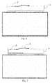
- a possible device with a housing 5 enclosing an antenna element 2 that is to be used at a relatively long wavelength compared to the size of the device is illustrated in fig. 1 .
- the housing 5 of the device is, as an example, shown mounted on a box-like structure.
- a solution to the problem of operating an antenna at a frequency implying a wavelength that is comparably long in relation to the size of a housing 5 of a device including the antenna can be seen in fig. 2 .
- planar antenna element 2 is made larger by folding twice in the box. In this way, the effective antenna surface becomes larger and therefore the efficiency of the antenna can be improved. Also, since the antenna is larger, the electric length of the antenna can be made longer permitting to send radio waves with a lower frequency/greater wavelength.
- the device with the housing 5 is depicted without a top cover in fig. 2 for simplicity of interpreting the figure. In reality, when deploying the device, it would also comprise a top cover to make the housing 5 completely enclose the antenna element and other electrical components inside the device to protect them. This is also true for the other figures of this application.
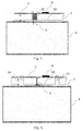
- fig. 3 It is an assembly 1 comprising an electrical device having a housing 5 comprising at least partly an electrically non-conductive material. Inside the housing 5 is located a planar antenna element 2 connected by a transmission line 3 to a radio circuit (not shown in the figure). The planar antenna element (2) further is connected to an electrically conducting connection member (9) which penetrates the housing (5)
- radio waves can be emitted by the antenna element 2 and propagate through the housing 5.
- the assembly can be seen to further comprise an electrically conductive structure 6, having an electrically conductive outer surface 7.
- the housing 5 of the electrical device is configured to be mechanically fastened to the electrically conductive structure 6 and the antenna element 2 inside the housing 5 is configured to be situated at least partly in parallel with the outer surface 7 of the electrically conductive structure 6 and to be in electrical connection with the outer surface 7 via the electrically conducting connection member 9 such that the electrically conductive structure 6 forms a radiating part when the antenna element 2 inside the housing 5 is excited by a radio signal from the radio circuit (not shown).
- this assembly increases the size of the radiating area of the assembly, compared to what is possible to contain in the device housing 5 alone, by employing the outer electrically conductive structure 6 as a radiating part of the antenna. Thereby, the efficiency of the assembly can be improved. It should be noticed that this antenna only has one excitation point and that the antenna element and the electrically conductive structure together forms one antenna. Thus, this assembly is not a system with two separate antennas excited with two different signals.
- the housing 5 When the assembly 1 is to be used to transmit a radio signal, the housing 5 would be fastened to the electrically conductive structure 6 and the antenna element 2 would be situated at least partly in parallel with said outer surface 7 and would be in electrical connection with the outer surface of the electrically conductive structure 6 via the connection member 9, as shown in fig. 3 .
- the housing of the device could be fastened to the electrically conductive structure 6 with the connection member 9.
- both the fastening of the device housing 5 to the electrically conductive structure 6 and the electrical connection of the antenna element 2 to the electrically conductive structure 6 can be effected with one and the same element 9, making the assembly 1 a bit less complicated. This is the case in fig. 3
- the electrically conductive structure could have an electrically conductive outer surface 7 with an area that is larger than an outer surface area 8 of the housing 5, which outer surface area 8 of the housing 5 is the largest outer surface area 8 of said housing 5. That is to say that the electrically conducting structure has an outer surface that is larger than what is possible to contain in the housing 5.
- the outer surface of the electrically conducting structure is therefore larger than the largest possible surface of an antenna element 2 contained inside the housing 5. This significantly increases the size of the radiating part of the antenna, compared to what is possible to contain in the housing 5 alone, such that a better efficiency is attained compared with what is available when the radiating part is contained in the housing 5. Therefore, in the case of a relatively small housing 5, compared to the resonating wavelength, a comparably large electrically conductive structure can compensate the size of the housing to provide an antenna that never-the-less has an acceptable efficiency.
- the electrical conductive outer surface 7 could have a physical extent that is equal to or less than 1 ⁇ 2 wavelengths of a resonating wavelength of the assembly.
- the surface 7 has a physical extent that is equal to or longer than 0.1 wavelengths of a resonating wavelength of the assembly.
- the antenna element 2 could for instance be formed by a printed circuit board 10. If at least a part of the antenna element 2 is flexible it could be bent 11 in the vicinity of where it connects to the connection member 9, as seen in fig. 3 . This is a convenient way of connecting the antenna element 2 to the electrically conducting structure while at the same time keeping the rest of the antenna element 2 at greater distance from the housing wall adjacent to the electrically conducting structure, as shown with the double arrow in fig. 3 .
- a plan view of the assembly 1 with, among others, the electrical device with he planar antenna element 2, the transmission line 3, the housing 5 of the electrical device, the electrically conductive structure 6 and the electrically conducting connection member 9 is visible.
- the antenna element 2 could be rigid and separated by a sleeve 12 from a bottom 13 of the device housing 5 in contact with the electrically conductive structure 6, as illustrated in fig 5 .
- the required distance of the antenna element 2 to the bottom 13 and the electrically conductive structure 6 could then be ensured while at the same time a single connection member 9, for instance a screw 9, could be used to connect it to the electrically conducting structure 6.
- the sleeve 12 may serve as a separating element only or additionally also as an electrically conducting element to connect the antenna element 2 to the electrically conductive structure 6 electrically.
- some other object may serve to provide the electrical contact between the antenna element 2 and the electrically conducting structure 6, for instance a spring 9 as seen in fig. 6 .
- the spring does not function to provide a support onto which the antenna element 2 may rest as was the case with the sleeve 12. Instead, the spring is compressed between the antenna element 2 and the bottom 13 of the device housing 5 as seen in fig. 6 where the antenna element 2 is resting on posts 14 and is holding the spring in compressed electrical contact with the electrically conductive structure 6.
- any other suitable electrical element may of course be used to provide the electrical contact between the antenna element 2 and the electrically conductive structure 6.
- the radio circuit 4 would be located in the housing 5. However, it is also possible that the radio circuit 4 is located elsewhere and the transmission line 3 would enter the housing 5 through a wall of the same (not shown in any figure).
- the radio circuit 4 When the radio circuit 4 is located in the housing 5, it is also possible to have the antenna element 2 and the radio circuit 4 located on the same printed circuit board. It reduces the count of components of the assembly 1 but may make the antenna more expensive if the PCB of the radio circuit 4 must use a multi layer design, rather than a two sided board that is enough for the antenna itself.
- a schematic illustration of the antenna element 2 and the radio circuit 4 located on the same printed circuit board is shown schematically in figure 5 . A single board can be seen in this sectioned side view.
- the antenna element 2 is configured to connect to the connection member 9 at a distance of less or equal to 0.1 wavelengths of a resonating wavelength of the assembly from a point 15 where the transmission line 3 connects to the antenna element 2 (see for instance fig. 3 ). This is due to the fact that the electrical length of the antenna element 2 often is about 0,25 wavelengths.
- the most distant part of the antenna element, seen from the point 15 where the transmission line connects to the antenna element - the excitation point of the antenna - has a higher electrical field strength and the part closer to the excitation point, has a lower electrical field strength and a higher current density and magnetic field.
- connection member 9 it is beneficial to connect connection member 9 at a point closer to the excitation point, so that the current is transferred from the antenna element through the connection 9 to the electrically conductive structure 6 (for instance a metal box).
- the best connection point for transferring the current from antenna and structure 6 is located within a distance less than 0.1 wavelengths from the excitation point of the antenna.
- the electrically conductive structure 6, where the housing 5 of the device is fastened is box-like and the assembly 1 can further comprise an electrically conducting sensor 16 that at least partly is introduced inside the electrically conductive structure 6, see fig. 7 .
- the sensor is denoted by a dashed line, reference numeral 16 is really pointing to the electrical line connecting to the sensor.
- the sensor can for instance be intended to register a physical parameter that is to be reported via a radio interface enabled by the assembly 1.
- a sensor is in this context understood to encompass any kind of sensor or measuring transducer that can be used to measure a quantity of some sort and report the measurement to some other entity. It may also encompass an electrical line transmitting a measurement from the sensor.
- electrically conductive means that some part of the sensor is electrically conductive at some frequency.
- the sensor would be in connection with a printed circuit board, in order to report any measurements.
- the printed circuit board, to which measurements from the sensor would be communicated would also be in connection with the radio circuit, in order to enable the measurements to be communicated wirelessly via the antenna element 2. It is not necessarily so that the radio circuit must be hosted on the PCB where the measurements from the sensor 16 are collected, but they must be in some kind of contact in order for such measurements to ultimately be communicated via the antenna element 2.
- the sensor may funnel some of the radio energy to the inside of the electrically conductive box where it is effectively dissipated as heat.
- the antenna element 2 is galvanically connected to the electrically conducting box. Without this connection to the electrically conducting box, the sensor effectively becomes a part of the radiating antenna. Having the antenna element directly connected to the electrically conductive box kind of short circuits the sensor in the sense that it does not any longer electrically form part of the antenna.
- the assembly 1 according to the invention could for instance be used in the VHF (Very High Frequency) band, making it a VHF antenna.
- VHF Very High Frequency
- 169 MHz frequency band could be used in some countries for different applications.
- the electrically conductive structure 6 could be a gas flow meter chamber to which the device housing 5 with the antenna element 2 would be attached to complete the assembly 1.
- the electrically conductive structure 6, can be made of metal such as aluminium or steel. However, other, electrically conductive materials are also possible and there is really only a need for the surface of the electrically conductive structure 6 to be electrically conductive. Thus, a design with a non-conductive material, coated with an electrically conductive coating is also possible. Such a coating could be metallic or even an electrically conductive synthetic material.
Landscapes
- Engineering & Computer Science (AREA)
- Computer Networks & Wireless Communication (AREA)
- Support Of Aerials (AREA)
Abstract
- an electrical device having a housing (5). Inside the housing is a planar antenna element (2) connected to a radio circuit. The planar antenna element (2) is connected to a connection member (9) which penetrates the housing (5),
- an electrically conductive structure (6), having an electrically conductive outer surface (7), wherein
- the housing (5) is configured to be mechanically fastened to the electrically conductive structure (6) and the antenna element (2) inside the housing (5) is configured to be situated at least partly in parallel with the outer surface (7) of the electrically conductive structure (6) and to be in electrical connection with the outer surface (7) via the electrically conducting connection member (9) such that the electrically conductive structure (6) forms a radiating part when the antenna element (2) inside the housing (5) is excited by a radio signal.
Description
- This invention relates to an assembly comprising a device with a planar antenna.
- With the proliferation of radio technology, many electrical devices are today equipped with a radio interface to enable wireless communication of information from/to such devices.
- For instance, stand-alone devices for measuring some physical parameter can be deployed somewhere in the field and report measurements only via such a radio interface, making them easy to deploy even in places difficult to access.
- Depending on the circumstances, different radio frequencies can be used for the radio interface. When comparatively low frequency bands, such as VHF (Very High Frequency), are used, there is a need for a relatively large antenna due to the long wavelength.
- When using a planar antenna in housings of devices which are small in comparison to the wavelength of the frequency with which they are to operate, there may be a problem with antenna efficiency, since the wavelength of the radio waves to be transmitted is considerably longer than the physical extent of the housing of the device and therefore also the antenna inside that housing.
- Thus, it may happen that a device that otherwise can be made reasonably small will have problems harbouring a larger antenna for a lower frequency band.
- One solution to this problem is to use planar antennas with slits to increase the electrical length of the antenna. In this way, the required frequency may be transmitted since the electrical length of the antenna element can be increased up till the minimum half wavelength while still being able to fit the antenna in a relatively small housing.
- However, such an antenna may never-the-less be quite inefficient in lower frequency bands. A poor efficiency results in higher energy consumption which is generally not desirable and outright detrimental when the device is operated on battery power. Also, a weak radio signal from the antenna lessens the reach of the signal and/or the possible rate of transmission of information.
- A further problem with devices that make use of such a described antenna arises when such devices are connected to some kind of sensor to measure for instance a physical parameter in an electrically conducting, box-like structure. When the antenna directly or indirectly share a common printed circuit board with circuits that are in contact with the sensor and further is operated on a comparatively low frequency, such a sensor can have a negative effect on the antenna efficiency.
- It is an object of the present invention to propose a solution for or a reduction of the problems of prior art. A main object is consequently to propose a device with a planar antenna with an improved efficiency.
- According to the invention, this is accomplished with an assembly having the features of
claim 1. - The solution to this problem according to the invention is to use an electrically conducting surface of a structure where a housing of the device is mounted, as a part of the radiating structure. In this way - thinking out of the box so to speak - the antenna of the device can be significantly increased in size by employing the outer electrically
conductive structure 6 as a part of the antenna. - This increases the antenna efficiency due to the larger effective antenna area compared to what can be housed in the device housing.
- The assembly additionally also solves the problem of antenna efficiency in connection with such devices having an antenna and which are also in contact with a sensor, a sensor that is at least partly introduced inside an electrically conducting box.
- According to the invention, the antenna element of the device is galvanically connected to the electrically conducting box to make the electrically conducting box a part of the resulting antenna. The connection of the antenna element to the electrically conducting box effectively short-circuits the sensor radio-wise in relation to the antenna element. Therefore, the printed circuit board is practically not a part of the resulting antenna and thus there is a much lower energy transfer to the sensor from the antenna element without the need for any additional components or measures.
- Embodiments exemplifying the invention will now be described, by means of the appended drawings, on which:
-
Fig. 1 illustrates a device with an antenna according to the prior art, -
Fig. 2 illustrates a device with an improved antenna, -
Fig. 3 illustrates a sectioned side view of a device with a further improved antenna in the form of an assembly, -
Fig. 4 illustrates the device with the further improved antenna in plan view, -
Fig. 5 illustrates a sectioned side view of a device with an antenna mounted with a sleeve spacer to an electrically conductive structure, -
Fig. 6 illustrates a sectioned side view of a device with an antenna that makes electrical contact with an electrically conductive structure with a compressed spring, and -
Fig. 7 illustrates an assembly with a sensor introduced into an electrically conducting box. - A possible device with a
housing 5 enclosing anantenna element 2 that is to be used at a relatively long wavelength compared to the size of the device is illustrated infig. 1 . Thehousing 5 of the device is, as an example, shown mounted on a box-like structure. - A solution to the problem of operating an antenna at a frequency implying a wavelength that is comparably long in relation to the size of a
housing 5 of a device including the antenna can be seen infig. 2 . - Here the
planar antenna element 2 is made larger by folding twice in the box. In this way, the effective antenna surface becomes larger and therefore the efficiency of the antenna can be improved. Also, since the antenna is larger, the electric length of the antenna can be made longer permitting to send radio waves with a lower frequency/greater wavelength. It should be noted that the device with thehousing 5 is depicted without a top cover infig. 2 for simplicity of interpreting the figure. In reality, when deploying the device, it would also comprise a top cover to make thehousing 5 completely enclose the antenna element and other electrical components inside the device to protect them. This is also true for the other figures of this application. - However, the solution of
fig. 2 - while an improvement over the device offig. 1 - may in some cases also not be completely satisfactory. For instance when there is a need to operate the antenna at a comparably low frequency. - To improve upon the device of
fig. 2 , a solution according tofig. 3 is proposed. It is anassembly 1 comprising an electrical device having ahousing 5 comprising at least partly an electrically non-conductive material. Inside thehousing 5 is located aplanar antenna element 2 connected by atransmission line 3 to a radio circuit (not shown in the figure). The planar antenna element (2) further is connected to an electrically conducting connection member (9) which penetrates the housing (5) - Since there is at least a part of the
housing 5 that is made in the non-conductive material, radio waves can be emitted by theantenna element 2 and propagate through thehousing 5. - The assembly can be seen to further comprise an electrically
conductive structure 6, having an electrically conductiveouter surface 7. - Further, the
housing 5 of the electrical device is configured to be mechanically fastened to the electricallyconductive structure 6 and theantenna element 2 inside thehousing 5 is configured to be situated at least partly in parallel with theouter surface 7 of the electricallyconductive structure 6 and to be in electrical connection with theouter surface 7 via the electrically conductingconnection member 9 such that the electricallyconductive structure 6 forms a radiating part when theantenna element 2 inside thehousing 5 is excited by a radio signal from the radio circuit (not shown). - This increases the size of the radiating area of the assembly, compared to what is possible to contain in the
device housing 5 alone, by employing the outer electricallyconductive structure 6 as a radiating part of the antenna. Thereby, the efficiency of the assembly can be improved. It should be noticed that this antenna only has one excitation point and that the antenna element and the electrically conductive structure together forms one antenna. Thus, this assembly is not a system with two separate antennas excited with two different signals. - When the
assembly 1 is to be used to transmit a radio signal, thehousing 5 would be fastened to the electricallyconductive structure 6 and theantenna element 2 would be situated at least partly in parallel with saidouter surface 7 and would be in electrical connection with the outer surface of the electricallyconductive structure 6 via theconnection member 9, as shown infig. 3 . - As a variant, the housing of the device could be fastened to the electrically
conductive structure 6 with theconnection member 9. In this way, both the fastening of the device housing 5 to the electricallyconductive structure 6 and the electrical connection of theantenna element 2 to the electricallyconductive structure 6 can be effected with one and thesame element 9, making the assembly 1 a bit less complicated. This is the case infig. 3 - The electrically conductive structure could have an electrically conductive
outer surface 7 with an area that is larger than anouter surface area 8 of thehousing 5, whichouter surface area 8 of thehousing 5 is the largestouter surface area 8 of saidhousing 5. That is to say that the electrically conducting structure has an outer surface that is larger than what is possible to contain in thehousing 5. The outer surface of the electrically conducting structure is therefore larger than the largest possible surface of anantenna element 2 contained inside thehousing 5. This significantly increases the size of the radiating part of the antenna, compared to what is possible to contain in thehousing 5 alone, such that a better efficiency is attained compared with what is available when the radiating part is contained in thehousing 5. Therefore, in the case of a relativelysmall housing 5, compared to the resonating wavelength, a comparably large electrically conductive structure can compensate the size of the housing to provide an antenna that never-the-less has an acceptable efficiency. - The electrical conductive
outer surface 7 could have a physical extent that is equal to or less than ½ wavelengths of a resonating wavelength of the assembly. The restriction on the physical extent of theelectrically conducting structure 6, that is that the actual size of the structure does not surpass said length when measured across theconductive surface 7 in any direction, sets an upper boundary of thestructure 6 to make sure it does not make the resulting antenna resemble a directive antenna. Thus, in this way a more omnidirectional characteristic of the resulting antenna is retained. - In order for the electrically conductive
outer surface 7 to make a meaningful contribution to the resulting antenna structure, it could be recommended that thesurface 7 has a physical extent that is equal to or longer than 0.1 wavelengths of a resonating wavelength of the assembly. - The
antenna element 2 could for instance be formed by a printedcircuit board 10. If at least a part of theantenna element 2 is flexible it could be bent 11 in the vicinity of where it connects to theconnection member 9, as seen infig. 3 . This is a convenient way of connecting theantenna element 2 to the electrically conducting structure while at the same time keeping the rest of theantenna element 2 at greater distance from the housing wall adjacent to the electrically conducting structure, as shown with the double arrow infig. 3 . - In
fig. 4 , a plan view of theassembly 1 with, among others, the electrical device with heplanar antenna element 2, thetransmission line 3, thehousing 5 of the electrical device, the electricallyconductive structure 6 and the electrically conductingconnection member 9 is visible. - As an alternative, the
antenna element 2 could be rigid and separated by asleeve 12 from a bottom 13 of thedevice housing 5 in contact with the electricallyconductive structure 6, as illustrated infig 5 . The required distance of theantenna element 2 to the bottom 13 and the electricallyconductive structure 6 could then be ensured while at the same time asingle connection member 9, for instance ascrew 9, could be used to connect it to the electrically conductingstructure 6. - The
sleeve 12 may serve as a separating element only or additionally also as an electrically conducting element to connect theantenna element 2 to the electricallyconductive structure 6 electrically. - Instead of a screw and/or a
sleeve 12 being theconnection member 9, some other object may serve to provide the electrical contact between theantenna element 2 and the electrically conductingstructure 6, for instance aspring 9 as seen infig. 6 . - In the case of
fig. 6 , the spring does not function to provide a support onto which theantenna element 2 may rest as was the case with thesleeve 12. Instead, the spring is compressed between theantenna element 2 and the bottom 13 of thedevice housing 5 as seen infig. 6 where theantenna element 2 is resting onposts 14 and is holding the spring in compressed electrical contact with the electricallyconductive structure 6. - Instead of a screw,
sleeve 12 or spring, any other suitable electrical element may of course be used to provide the electrical contact between theantenna element 2 and the electricallyconductive structure 6. - Ordinarily, the
radio circuit 4 would be located in thehousing 5. However, it is also possible that theradio circuit 4 is located elsewhere and thetransmission line 3 would enter thehousing 5 through a wall of the same (not shown in any figure). - When the
radio circuit 4 is located in thehousing 5, it is also possible to have theantenna element 2 and theradio circuit 4 located on the same printed circuit board. It reduces the count of components of theassembly 1 but may make the antenna more expensive if the PCB of theradio circuit 4 must use a multi layer design, rather than a two sided board that is enough for the antenna itself. A schematic illustration of theantenna element 2 and theradio circuit 4 located on the same printed circuit board is shown schematically infigure 5 . A single board can be seen in this sectioned side view. - It has been found that in some cases it is beneficial if the
antenna element 2 is configured to connect to theconnection member 9 at a distance of less or equal to 0.1 wavelengths of a resonating wavelength of the assembly from apoint 15 where thetransmission line 3 connects to the antenna element 2 (see for instancefig. 3 ). This is due to the fact that the electrical length of theantenna element 2 often is about 0,25 wavelengths. The most distant part of the antenna element, seen from thepoint 15 where the transmission line connects to the antenna element - the excitation point of the antenna - has a higher electrical field strength and the part closer to the excitation point, has a lower electrical field strength and a higher current density and magnetic field. To get an improvement, it is beneficial to connectconnection member 9 at a point closer to the excitation point, so that the current is transferred from the antenna element through theconnection 9 to the electrically conductive structure 6 (for instance a metal box). The best connection point for transferring the current from antenna andstructure 6 is located within a distance less than 0.1 wavelengths from the excitation point of the antenna. - In some embodiments, the electrically
conductive structure 6, where thehousing 5 of the device is fastened, is box-like and theassembly 1 can further comprise an electrically conductingsensor 16 that at least partly is introduced inside the electricallyconductive structure 6, seefig. 7 . Infigure 7 , the sensor is denoted by a dashed line,reference numeral 16 is really pointing to the electrical line connecting to the sensor. The sensor can for instance be intended to register a physical parameter that is to be reported via a radio interface enabled by theassembly 1. As such, a sensor is in this context understood to encompass any kind of sensor or measuring transducer that can be used to measure a quantity of some sort and report the measurement to some other entity. It may also encompass an electrical line transmitting a measurement from the sensor. Further, electrically conductive means that some part of the sensor is electrically conductive at some frequency. - The sensor would be in connection with a printed circuit board, in order to report any measurements. The printed circuit board, to which measurements from the sensor would be communicated, would also be in connection with the radio circuit, in order to enable the measurements to be communicated wirelessly via the
antenna element 2. It is not necessarily so that the radio circuit must be hosted on the PCB where the measurements from thesensor 16 are collected, but they must be in some kind of contact in order for such measurements to ultimately be communicated via theantenna element 2. - In such an embodiment, with an
antenna element 2 in connection with a sensor that is at least partly introduced into a hollow, box-like, electricallyconductive structure 6, there might be a problem with the efficiency of the antenna. - The reason for this inefficiency has been realised by the present applicant to be that the sensor may funnel some of the radio energy to the inside of the electrically conductive box where it is effectively dissipated as heat.
- Having this insight, a possible solution would be to apply an electric filter to the sensor and situate such a filter before the entrance point to the electrically conductive box to filter out the frequencies of the antenna. This would lessen the amount of antenna energy transferred into the box and increase antenna gain. A drawback with that solution is that it requires filter components, adding to the cost and complexity of such a design.
- It turns out that this further problem can be circumvented by the design of an
assembly 1 according to this invention. The heart of the solution is that theantenna element 2 is galvanically connected to the electrically conducting box. Without this connection to the electrically conducting box, the sensor effectively becomes a part of the radiating antenna. Having the antenna element directly connected to the electrically conductive box kind of short circuits the sensor in the sense that it does not any longer electrically form part of the antenna. - Thus, there is no longer any need for a filter and the antenna efficiency is improved since the radio energy is properly radiated in the way it was intended and not through the sensor.
- The
assembly 1 according to the invention could for instance be used in the VHF (Very High Frequency) band, making it a VHF antenna. For example the 169 MHz frequency band could be used in some countries for different applications. - Such an application would be to use the
assembly 1 according to the invention to communicate gas flow measurements, for instance by public utilities measuring consumption of coal gas. In such a case, the electricallyconductive structure 6 could be a gas flow meter chamber to which thedevice housing 5 with theantenna element 2 would be attached to complete theassembly 1. - The electrically
conductive structure 6, what ever form it takes, can be made of metal such as aluminium or steel. However, other, electrically conductive materials are also possible and there is really only a need for the surface of the electricallyconductive structure 6 to be electrically conductive. Thus, a design with a non-conductive material, coated with an electrically conductive coating is also possible. Such a coating could be metallic or even an electrically conductive synthetic material. -
- 1. Assembly
- 2. Planar antenna element
- 3. Transmission line
- 4. Radio circuit
- 5. Housing
- 6. Electrically conductive structure
- 7. Electrically conductive outer surface of the electrically conductive structure
- 8. Outer surface area of the housing
- 9. Electrically conducting connection member
- 10. Printed circuit board
- 11. Bending
- 12. Sleeve
- 13. Bottom of the housing
- 14. Post
- 15. Point where the transmission line connects to the antenna electrically
- 16. Line connecting to electrically conducting sensor
Claims (15)
- Assembly (1) comprising:- an electrical device having a housing (5) comprising at least partly an electrically non-conductive material, wherein inside the housing is located a planar antenna element (2) connected by a transmission line (3) to a radio circuit (4), wherein the planar antenna element (2) further is connected to an electrically conducting connection member (9) which penetrates the housing (5),- an electrically conductive structure (6) having an electrically conductive outer surface (7), wherein- the housing (5) of the electrical device is configured to be mechanically fastened to the electrically conductive structure (6) and the antenna element (2) inside the housing (5) is configured to be situated at least partly in parallel with the outer surface (7) of the electrically conductive structure (6) and to be in electrical connection with the outer surface (7) via the electrically conducting connection member (9) such that the electrically conductive structure (6) forms a radiating part when the antenna element (2) inside the housing (5) is excited by a radio signal from the radio circuit (4).
- Assembly (1) according to claim 1, wherein the housing (5) is fastened to the electrically conductive structure (6) and the antenna element (2) is situated at least partly in parallel with said outer surface (7) and is in electrical connection with the outer surface of the electrically conductive structure (6) via the connection member (9).
- Assembly (1) according to claim 2, wherein the housing is fastened to the electrically conductive structure (6) with the connection member (9).
- Assembly (1) according to any of claims 1-3, wherein the electrically conducting structure has an electrically conductive outer surface (7) with an area that is larger than an outer surface area (8) of the device housing (5), which outer surface area (8) of the device housing (5) is the largest outer surface area (8) of said device housing (5).
- Assembly (1) according to any of claims 1-4, wherein the electrically conductive outer surface (7) has a physical extent that is equal to or less than ½ wavelengths of a resonating wavelength of the assembly.
- Assembly (1) according to any of claims 1-5, wherein the electrically conductive outer surface (7) has a physical extent that is equal to or larger than 0.1 wavelengths of a resonating wavelength of the assembly.
- Assembly (1) according to any of claims 1-6, wherein the antenna element (2) comprises a printed circuit board (10).
- Assembly (1) according to any of claims 1-7, wherein at least a part of the antenna element (2) is flexible and is bent (11) in the vicinity of where it connects to the connection member (9).
- Assembly (1) according to any of claims 1-7, wherein the antenna element (2) is rigid and separated by a sleeve (12) from a bottom (13) of the device housing (5) in contact with the electrically conductive structure (6).
- Assembly (1) according to any of claims 1-9, wherein the radio circuit (4) is located in the device housing (5).
- Assembly (1) according to claim 10, wherein the antenna element (2) and the radio circuit (4) are located on the same printed circuit board.
- Assembly (1) according to any of claims 1-11, wherein the antenna element (2) is configured to connect to the connection member (9) at a distance of less or equal to 0.1 wavelength of a resonating wavelength of the assembly from a point (15) where the transmission line (3) connects to the antenna element (2).
- Assembly (1) according to any of claims 1-12, wherein the electrically conductive structure (6) is box-like and the assembly (1) further comprises an electrically conducting sensor, at least partly introduced inside the electrically conductive structure (6) and is in connection with a printed circuit board, which printed circuit board is also in connection with the radio circuit (4).
- Assembly (1) according to any of claims 1-13, wherein the antenna is a VHF antenna.
- Assembly (1) according to any of claims 1-14, wherein the electrically conductive structure (6) is a gas flow meter chamber.
Priority Applications (1)
| Application Number | Priority Date | Filing Date | Title |
|---|---|---|---|
| EP12182491.6A EP2704251A1 (en) | 2012-08-30 | 2012-08-30 | Assembly comprising a device with a planar antenna |
Applications Claiming Priority (1)
| Application Number | Priority Date | Filing Date | Title |
|---|---|---|---|
| EP12182491.6A EP2704251A1 (en) | 2012-08-30 | 2012-08-30 | Assembly comprising a device with a planar antenna |
Publications (1)
| Publication Number | Publication Date |
|---|---|
| EP2704251A1 true EP2704251A1 (en) | 2014-03-05 |
Family
ID=47048956
Family Applications (1)
| Application Number | Title | Priority Date | Filing Date |
|---|---|---|---|
| EP12182491.6A Withdrawn EP2704251A1 (en) | 2012-08-30 | 2012-08-30 | Assembly comprising a device with a planar antenna |
Country Status (1)
| Country | Link |
|---|---|
| EP (1) | EP2704251A1 (en) |
Citations (4)
| Publication number | Priority date | Publication date | Assignee | Title |
|---|---|---|---|---|
| US6731920B1 (en) * | 2000-03-31 | 2004-05-04 | Matsushita Electric Industrial Co., Ltd. | Portable telephone apparatus and control method thereof |
| US20060017626A1 (en) * | 2004-07-12 | 2006-01-26 | Anand Kannan | Antenna module for mobile phone |
| FR2888068A1 (en) * | 2005-07-01 | 2007-01-05 | Agnes Jullian | Street furniture element e.g. public lighting lamp post, communication function rendering device for e.g. remotely reading gas meter, has wireless and wire data transmission, emission and/or reception units to control external peripherals |
| US20110254741A1 (en) * | 2010-04-16 | 2011-10-20 | Katsunori Ishimiya | Wireless communication device with housing member that functions as a radiating element of an antenna |
-
2012
- 2012-08-30 EP EP12182491.6A patent/EP2704251A1/en not_active Withdrawn
Patent Citations (4)
| Publication number | Priority date | Publication date | Assignee | Title |
|---|---|---|---|---|
| US6731920B1 (en) * | 2000-03-31 | 2004-05-04 | Matsushita Electric Industrial Co., Ltd. | Portable telephone apparatus and control method thereof |
| US20060017626A1 (en) * | 2004-07-12 | 2006-01-26 | Anand Kannan | Antenna module for mobile phone |
| FR2888068A1 (en) * | 2005-07-01 | 2007-01-05 | Agnes Jullian | Street furniture element e.g. public lighting lamp post, communication function rendering device for e.g. remotely reading gas meter, has wireless and wire data transmission, emission and/or reception units to control external peripherals |
| US20110254741A1 (en) * | 2010-04-16 | 2011-10-20 | Katsunori Ishimiya | Wireless communication device with housing member that functions as a radiating element of an antenna |
Similar Documents
| Publication | Publication Date | Title |
|---|---|---|
| US9048538B2 (en) | Antenna assembly and wireless communication device employing same | |
| JP5686221B2 (en) | ANTENNA DEVICE AND RADIO DEVICE INCLUDING THE SAME | |
| WO2012021751A3 (en) | Improved omni-directional antenna system for wireless communication | |
| CN1826707A (en) | Antenna assembly for connecting external equipment to radio equipment | |
| US20120132718A1 (en) | Transponder tagged object and method for manufacturing a transponder tagged object | |
| TWI487202B (en) | Antenna module | |
| US20160305807A1 (en) | Consumption Meter Comprising A Foldable Printed Circuit Board Assembly | |
| JP2015043572A (en) | Antenna and radio communication device including the same | |
| JP5510836B2 (en) | ANTENNA AND RADIO DEVICE HAVING THE SAME | |
| CN207851522U (en) | watch device | |
| JP6436100B2 (en) | ANTENNA DEVICE AND RADIO DEVICE INCLUDING THE SAME | |
| CN104733852B (en) | Antenna structure and wireless communication device using same | |
| CN107078374A (en) | Antenna module and electronic installation | |
| KR101126606B1 (en) | A rear case of mobile phone combination with loop antenna | |
| EP2704251A1 (en) | Assembly comprising a device with a planar antenna | |
| WO2013187013A1 (en) | Wireless device | |
| CN105990638A (en) | electronic device | |
| CN105307432A (en) | Electronic device and manufacturing method thereof | |
| US20230060856A1 (en) | Microphone Antenna for Wireless Microphone Applications | |
| CN103633435B (en) | The antenna structure of conformable metallic shell | |
| TW201445813A (en) | Antenna assembly, wireless communication device and manufacturing method employing same | |
| CN102394384A (en) | Mobile equipment, mobile phone and antenna structure thereof | |
| JP5725415B2 (en) | ANTENNA DEVICE AND WIRELESS COMMUNICATION DEVICE | |
| JP7556159B2 (en) | Antenna Unit and Transmitter | |
| JP7607142B2 (en) | Parasitic element |
Legal Events
| Date | Code | Title | Description |
|---|---|---|---|
| AK | Designated contracting states |
Kind code of ref document: A1 Designated state(s): AL AT BE BG CH CY CZ DE DK EE ES FI FR GB GR HR HU IE IS IT LI LT LU LV MC MK MT NL NO PL PT RO RS SE SI SK SM TR |
|
| AX | Request for extension of the european patent |
Extension state: BA ME |
|
| PUAI | Public reference made under article 153(3) epc to a published international application that has entered the european phase |
Free format text: ORIGINAL CODE: 0009012 |
|
| 17P | Request for examination filed |
Effective date: 20140904 |
|
| RBV | Designated contracting states (corrected) |
Designated state(s): AL AT BE BG CH CY CZ DE DK EE ES FI FR GB GR HR HU IE IS IT LI LT LU LV MC MK MT NL NO PL PT RO RS SE SI SK SM TR |
|
| STAA | Information on the status of an ep patent application or granted ep patent |
Free format text: STATUS: THE APPLICATION HAS BEEN WITHDRAWN |
|
| 18W | Application withdrawn |
Effective date: 20161104 |