EP2703883A1 - Substrate for a liquid crystal display device and method of manufacturing it - Google Patents
Substrate for a liquid crystal display device and method of manufacturing it Download PDFInfo
- Publication number
- EP2703883A1 EP2703883A1 EP13182702.4A EP13182702A EP2703883A1 EP 2703883 A1 EP2703883 A1 EP 2703883A1 EP 13182702 A EP13182702 A EP 13182702A EP 2703883 A1 EP2703883 A1 EP 2703883A1
- Authority
- EP
- European Patent Office
- Prior art keywords
- gate line
- array substrate
- width
- electrode
- gate
- Prior art date
- Legal status (The legal status is an assumption and is not a legal conclusion. Google has not performed a legal analysis and makes no representation as to the accuracy of the status listed.)
- Ceased
Links
Images


Classifications
-
- G—PHYSICS
- G02—OPTICS
- G02F—OPTICAL DEVICES OR ARRANGEMENTS FOR THE CONTROL OF LIGHT BY MODIFICATION OF THE OPTICAL PROPERTIES OF THE MEDIA OF THE ELEMENTS INVOLVED THEREIN; NON-LINEAR OPTICS; FREQUENCY-CHANGING OF LIGHT; OPTICAL LOGIC ELEMENTS; OPTICAL ANALOGUE/DIGITAL CONVERTERS
- G02F1/00—Devices or arrangements for the control of the intensity, colour, phase, polarisation or direction of light arriving from an independent light source, e.g. switching, gating or modulating; Non-linear optics
- G02F1/01—Devices or arrangements for the control of the intensity, colour, phase, polarisation or direction of light arriving from an independent light source, e.g. switching, gating or modulating; Non-linear optics for the control of the intensity, phase, polarisation or colour
- G02F1/13—Devices or arrangements for the control of the intensity, colour, phase, polarisation or direction of light arriving from an independent light source, e.g. switching, gating or modulating; Non-linear optics for the control of the intensity, phase, polarisation or colour based on liquid crystals, e.g. single liquid crystal display cells
- G02F1/133—Constructional arrangements; Operation of liquid crystal cells; Circuit arrangements
- G02F1/136—Liquid crystal cells structurally associated with a semi-conducting layer or substrate, e.g. cells forming part of an integrated circuit
- G02F1/1362—Active matrix addressed cells
- G02F1/136227—Through-hole connection of the pixel electrode to the active element through an insulation layer
-
- G—PHYSICS
- G02—OPTICS
- G02F—OPTICAL DEVICES OR ARRANGEMENTS FOR THE CONTROL OF LIGHT BY MODIFICATION OF THE OPTICAL PROPERTIES OF THE MEDIA OF THE ELEMENTS INVOLVED THEREIN; NON-LINEAR OPTICS; FREQUENCY-CHANGING OF LIGHT; OPTICAL LOGIC ELEMENTS; OPTICAL ANALOGUE/DIGITAL CONVERTERS
- G02F1/00—Devices or arrangements for the control of the intensity, colour, phase, polarisation or direction of light arriving from an independent light source, e.g. switching, gating or modulating; Non-linear optics
- G02F1/01—Devices or arrangements for the control of the intensity, colour, phase, polarisation or direction of light arriving from an independent light source, e.g. switching, gating or modulating; Non-linear optics for the control of the intensity, phase, polarisation or colour
- G02F1/13—Devices or arrangements for the control of the intensity, colour, phase, polarisation or direction of light arriving from an independent light source, e.g. switching, gating or modulating; Non-linear optics for the control of the intensity, phase, polarisation or colour based on liquid crystals, e.g. single liquid crystal display cells
- G02F1/133—Constructional arrangements; Operation of liquid crystal cells; Circuit arrangements
- G02F1/1333—Constructional arrangements; Manufacturing methods
- G02F1/1343—Electrodes
- G02F1/134309—Electrodes characterised by their geometrical arrangement
-
- G—PHYSICS
- G02—OPTICS
- G02F—OPTICAL DEVICES OR ARRANGEMENTS FOR THE CONTROL OF LIGHT BY MODIFICATION OF THE OPTICAL PROPERTIES OF THE MEDIA OF THE ELEMENTS INVOLVED THEREIN; NON-LINEAR OPTICS; FREQUENCY-CHANGING OF LIGHT; OPTICAL LOGIC ELEMENTS; OPTICAL ANALOGUE/DIGITAL CONVERTERS
- G02F1/00—Devices or arrangements for the control of the intensity, colour, phase, polarisation or direction of light arriving from an independent light source, e.g. switching, gating or modulating; Non-linear optics
- G02F1/01—Devices or arrangements for the control of the intensity, colour, phase, polarisation or direction of light arriving from an independent light source, e.g. switching, gating or modulating; Non-linear optics for the control of the intensity, phase, polarisation or colour
- G02F1/13—Devices or arrangements for the control of the intensity, colour, phase, polarisation or direction of light arriving from an independent light source, e.g. switching, gating or modulating; Non-linear optics for the control of the intensity, phase, polarisation or colour based on liquid crystals, e.g. single liquid crystal display cells
- G02F1/133—Constructional arrangements; Operation of liquid crystal cells; Circuit arrangements
- G02F1/136—Liquid crystal cells structurally associated with a semi-conducting layer or substrate, e.g. cells forming part of an integrated circuit
- G02F1/1362—Active matrix addressed cells
- G02F1/136286—Wiring, e.g. gate line, drain line
-
- G—PHYSICS
- G02—OPTICS
- G02F—OPTICAL DEVICES OR ARRANGEMENTS FOR THE CONTROL OF LIGHT BY MODIFICATION OF THE OPTICAL PROPERTIES OF THE MEDIA OF THE ELEMENTS INVOLVED THEREIN; NON-LINEAR OPTICS; FREQUENCY-CHANGING OF LIGHT; OPTICAL LOGIC ELEMENTS; OPTICAL ANALOGUE/DIGITAL CONVERTERS
- G02F1/00—Devices or arrangements for the control of the intensity, colour, phase, polarisation or direction of light arriving from an independent light source, e.g. switching, gating or modulating; Non-linear optics
- G02F1/01—Devices or arrangements for the control of the intensity, colour, phase, polarisation or direction of light arriving from an independent light source, e.g. switching, gating or modulating; Non-linear optics for the control of the intensity, phase, polarisation or colour
- G02F1/13—Devices or arrangements for the control of the intensity, colour, phase, polarisation or direction of light arriving from an independent light source, e.g. switching, gating or modulating; Non-linear optics for the control of the intensity, phase, polarisation or colour based on liquid crystals, e.g. single liquid crystal display cells
- G02F1/133—Constructional arrangements; Operation of liquid crystal cells; Circuit arrangements
- G02F1/1333—Constructional arrangements; Manufacturing methods
- G02F1/1335—Structural association of cells with optical devices, e.g. polarisers or reflectors
- G02F1/133509—Filters, e.g. light shielding masks
- G02F1/133512—Light shielding layers, e.g. black matrix
-
- G—PHYSICS
- G02—OPTICS
- G02F—OPTICAL DEVICES OR ARRANGEMENTS FOR THE CONTROL OF LIGHT BY MODIFICATION OF THE OPTICAL PROPERTIES OF THE MEDIA OF THE ELEMENTS INVOLVED THEREIN; NON-LINEAR OPTICS; FREQUENCY-CHANGING OF LIGHT; OPTICAL LOGIC ELEMENTS; OPTICAL ANALOGUE/DIGITAL CONVERTERS
- G02F1/00—Devices or arrangements for the control of the intensity, colour, phase, polarisation or direction of light arriving from an independent light source, e.g. switching, gating or modulating; Non-linear optics
- G02F1/01—Devices or arrangements for the control of the intensity, colour, phase, polarisation or direction of light arriving from an independent light source, e.g. switching, gating or modulating; Non-linear optics for the control of the intensity, phase, polarisation or colour
- G02F1/13—Devices or arrangements for the control of the intensity, colour, phase, polarisation or direction of light arriving from an independent light source, e.g. switching, gating or modulating; Non-linear optics for the control of the intensity, phase, polarisation or colour based on liquid crystals, e.g. single liquid crystal display cells
- G02F1/133—Constructional arrangements; Operation of liquid crystal cells; Circuit arrangements
- G02F1/1333—Constructional arrangements; Manufacturing methods
- G02F1/1343—Electrodes
- G02F1/134309—Electrodes characterised by their geometrical arrangement
- G02F1/134318—Electrodes characterised by their geometrical arrangement having a patterned common electrode
-
- G—PHYSICS
- G02—OPTICS
- G02F—OPTICAL DEVICES OR ARRANGEMENTS FOR THE CONTROL OF LIGHT BY MODIFICATION OF THE OPTICAL PROPERTIES OF THE MEDIA OF THE ELEMENTS INVOLVED THEREIN; NON-LINEAR OPTICS; FREQUENCY-CHANGING OF LIGHT; OPTICAL LOGIC ELEMENTS; OPTICAL ANALOGUE/DIGITAL CONVERTERS
- G02F1/00—Devices or arrangements for the control of the intensity, colour, phase, polarisation or direction of light arriving from an independent light source, e.g. switching, gating or modulating; Non-linear optics
- G02F1/01—Devices or arrangements for the control of the intensity, colour, phase, polarisation or direction of light arriving from an independent light source, e.g. switching, gating or modulating; Non-linear optics for the control of the intensity, phase, polarisation or colour
- G02F1/13—Devices or arrangements for the control of the intensity, colour, phase, polarisation or direction of light arriving from an independent light source, e.g. switching, gating or modulating; Non-linear optics for the control of the intensity, phase, polarisation or colour based on liquid crystals, e.g. single liquid crystal display cells
- G02F1/133—Constructional arrangements; Operation of liquid crystal cells; Circuit arrangements
- G02F1/1333—Constructional arrangements; Manufacturing methods
- G02F1/1343—Electrodes
- G02F1/134309—Electrodes characterised by their geometrical arrangement
- G02F1/134372—Electrodes characterised by their geometrical arrangement for fringe field switching [FFS] where the common electrode is not patterned
-
- G—PHYSICS
- G02—OPTICS
- G02F—OPTICAL DEVICES OR ARRANGEMENTS FOR THE CONTROL OF LIGHT BY MODIFICATION OF THE OPTICAL PROPERTIES OF THE MEDIA OF THE ELEMENTS INVOLVED THEREIN; NON-LINEAR OPTICS; FREQUENCY-CHANGING OF LIGHT; OPTICAL LOGIC ELEMENTS; OPTICAL ANALOGUE/DIGITAL CONVERTERS
- G02F1/00—Devices or arrangements for the control of the intensity, colour, phase, polarisation or direction of light arriving from an independent light source, e.g. switching, gating or modulating; Non-linear optics
- G02F1/01—Devices or arrangements for the control of the intensity, colour, phase, polarisation or direction of light arriving from an independent light source, e.g. switching, gating or modulating; Non-linear optics for the control of the intensity, phase, polarisation or colour
- G02F1/13—Devices or arrangements for the control of the intensity, colour, phase, polarisation or direction of light arriving from an independent light source, e.g. switching, gating or modulating; Non-linear optics for the control of the intensity, phase, polarisation or colour based on liquid crystals, e.g. single liquid crystal display cells
- G02F1/133—Constructional arrangements; Operation of liquid crystal cells; Circuit arrangements
- G02F1/1333—Constructional arrangements; Manufacturing methods
- G02F1/1343—Electrodes
- G02F1/134309—Electrodes characterised by their geometrical arrangement
- G02F1/134381—Hybrid switching mode, i.e. for applying an electric field with components parallel and orthogonal to the substrates
-
- G—PHYSICS
- G02—OPTICS
- G02F—OPTICAL DEVICES OR ARRANGEMENTS FOR THE CONTROL OF LIGHT BY MODIFICATION OF THE OPTICAL PROPERTIES OF THE MEDIA OF THE ELEMENTS INVOLVED THEREIN; NON-LINEAR OPTICS; FREQUENCY-CHANGING OF LIGHT; OPTICAL LOGIC ELEMENTS; OPTICAL ANALOGUE/DIGITAL CONVERTERS
- G02F1/00—Devices or arrangements for the control of the intensity, colour, phase, polarisation or direction of light arriving from an independent light source, e.g. switching, gating or modulating; Non-linear optics
- G02F1/01—Devices or arrangements for the control of the intensity, colour, phase, polarisation or direction of light arriving from an independent light source, e.g. switching, gating or modulating; Non-linear optics for the control of the intensity, phase, polarisation or colour
- G02F1/13—Devices or arrangements for the control of the intensity, colour, phase, polarisation or direction of light arriving from an independent light source, e.g. switching, gating or modulating; Non-linear optics for the control of the intensity, phase, polarisation or colour based on liquid crystals, e.g. single liquid crystal display cells
- G02F1/133—Constructional arrangements; Operation of liquid crystal cells; Circuit arrangements
- G02F1/136—Liquid crystal cells structurally associated with a semi-conducting layer or substrate, e.g. cells forming part of an integrated circuit
- G02F1/1362—Active matrix addressed cells
- G02F1/136218—Shield electrodes
-
- G—PHYSICS
- G02—OPTICS
- G02F—OPTICAL DEVICES OR ARRANGEMENTS FOR THE CONTROL OF LIGHT BY MODIFICATION OF THE OPTICAL PROPERTIES OF THE MEDIA OF THE ELEMENTS INVOLVED THEREIN; NON-LINEAR OPTICS; FREQUENCY-CHANGING OF LIGHT; OPTICAL LOGIC ELEMENTS; OPTICAL ANALOGUE/DIGITAL CONVERTERS
- G02F2201/00—Constructional arrangements not provided for in groups G02F1/00 - G02F7/00
- G02F2201/40—Arrangements for improving the aperture ratio
Definitions
- Embodiments of the invention relate to the field of display fabrication technologies, more particularly, to an array substrate, a method for manufacturing the same, and a display device comprising the array substrate.
- AD-SDS Advanced-Super Dimensional Switching
- ADS Advanced-Super Dimensional Switching
- a multi-dimensional electric field is formed with both a parallel electric field produced at edges of pixel electrodes on the same plane and a vertical electric field produced between a pixel electrode layer and a common electrode layer, so that liquid crystal molecules at all orientations, which are located directly above the electrodes and between the pixel electrodes in a liquid crystal cell, can be rotated and aligned, which enhances the work efficiency of planar-oriented liquid crystals and increases light transmittance.
- the Advanced-Super Dimensional Switching technology can improve the picture quality of TFT-LCDs and has advantages of high transmittance, wide viewing angles, high opening ratio, low chromatic aberration, low response time, no push Mura, etc.
- the ADS technology optimizes the liquid crystal material by means of electrodynamics and achieves a light efficiency of 90 percent of negative liquid crystals for positive liquid crystals, thereby solving the problem of low response time caused by the large viscosity of negative liquid crystals. Moreover, the ADS technology provides notable improvements in light transmittance, contrast ratio, brightness, viewing angle, chromatic aberration and so on.
- a black matrix (BM) for shielding light leaked from gate line normally has a minimum width of 32 ⁇ m, such that light leakage of the gate line is reduced to the maximum extent while a relatively optimal aperture ratio for the pixel element may be obtained.
- the aperture ratio is an important factor in determining the brightness and the power consumption of the display device -- the higher the aperture ratio is, the higher the light transmittance is, therefore the brighter the screen will be, under the same backlight condition.
- the power consumption of the backlight source in the LCD display takes up about 60% of the whole power output, therefore, a design with an aperture ratio as high as possible should be employed provided that the process conditions can be met, such that the power consumption of the backlight source may be minimized while the brightness requirement of the display device is met, thereby lowering the power consumption of the whole display system.
- the ADS-mode display device it needs to reduce the width of the BMs in order to improve the aperture ratio of the pixel element, which will lead to and exaggerate light leakage of the gate line.
- An I-ADS mode display device with high transmittance is proposed for the purpose of improving the aperture ratio of the pixel element while reducing light leakage of the gate line.
- the difference between the I-ADS mode and ADS mode display devices lies in that the positions of the pixel electrode and the common electrode in the array substrate are inverted. That is, in the I-ADS mode array substrate, the array substrate is disposed as the first electrode (first ITO, that is the plate-like electrode) on the substrate and the common electrode is disposed as the second electrode (second ITO, that is a slit electrode) above the pixel electrode; while in the ADS mode array substrate, the common electrode is disposed as the first electrode on the substrate, and the pixel electrode is disposed as the second electrode above the common electrode.
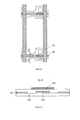
- Fig. 1(a) schematically illustrates a configuration of a conventional I-ADS mode array substrate and Fig. 1(b) is a cross section taken along A-A' of Fig. 1(a) .
- the I-ADS mode array substrate comprises a substrate 104, a gate line 103 and a pixel electrode 101 disposed on the substrate 104, and a common electrode 102 disposed above and completely overlaying the gate line 103.
- common electrode shielding effect is generated due to the common electrode 102 completely overlays the gate line 103, such that light leakage of the gate line is minimized, therefore the width of the BM for shielding light leaked from the gate line may be reduced, which helps to improve the aperture ratio of the pixel element.
- the common electrode completely overlaying the gate line that causes ratio of the gate electrode capacitance (C_gate) to increase and the line load of the gate line to increase, thereby causing a gate line delay and affecting the charge rate and charge efficiency of the display device.
- Embodiments of the invention provide an array substrate that can decrease the gate line load while improving the aperture ratio of the pixel element, and a display device comprising the array substrate.
- a first aspect of the invention provides an array substrate comprising a substrate, a gate line and a pixel electrode disposed on the substrate, and a common electrode disposed above and overlaying the gate line, wherein a strip-shaped through hole is disposed on the common electrode and at least a portion of the strip-shaped through hole is positioned right above the gate line.
- all of the strip-shaped through hole is positioned right above the gate line.
- a width of the strip-shaped through hole is larger than zero but smaller than a width of the gate line.
- the width of the gate line is smaller than a width of the common electrode.
- an insulating layer is disposed between the pixel electrode and the common electrode.
- a second aspect of the invention provides a display device comprising the above array substrate.
- a third aspect of the invention provides a method for manufacturing an array substrate comprising:
- the common electrode has a strip-shaped through hole and overlays the gate electrode, and at least a portion of the strip-shaped through hole being positioned right above the gate line.
- Fig. 1(a) schematically illustrates a configuration of a conventional array substrate with I-ADS mode
- Fig. 1(b) is a cross section taken along A-A' of the array substrate of Fig. 1(a) ;
- Fig. 2 schematically illustrates a configuration of an array substrate in accordance with an embodiment of the invention
- Fig. 3 is a graph schematically illustrating relationships between a width of a strip-shaped through hole disposed on a common electrode 102, a minimum width of a BM, a gate line light leakage region and ratio of C_gate of the array substrate in accordance with the embodiment of the invention;
- Fig. 4 schematically illustrates a configuration of a strip-shaped through hole in the array substrate in accordance with the embodiment of the invention.
- an array substrate in accordance with an embodiment of the invention comprises a substrate 204, a gate line 203 and a pixel electrode 201 disposed on the substrate 204, a common electrode 202 disposed above and overlaying the gate line 203.
- An insulating layer is disposed between the pixel electrode 201 and the common electrode 202.
- the array substrate may further comprises a data line, a plurality of pixel elements (each of which comprises a TFT) defined by intersections of the data line and the gate line, and a common electrode line etc, all of which will not be described herein as they are irrelevant to the inventive array substrate.
- a strip-shaped through hole with a width d1 is disposed on the common electrode 202; the strip-shaped through hole extends across the common electrode 202 along a direction parallel to the gate line 203 and is right above the gate line 203. In other embodiments, at least a portion of the strip-shaped through hole is positioned right above the gate line.
- the width d1 of the strip-shaped through hole is larger than zero but smaller than a width d2 of the gate line 203. More preferably, the width d2 of the gate line 203 is smaller than a width d3 of the common electrode 202 on both sides of the strip-shaped through hole.
- Fig. 3 is a graph schematically illustrates relationships between the width d1 of the strip-shaped through hole disposed on the common electrode 202 and a minimum width of a BM for shielding light leaked from the gate line, a width of a gate line light leakage region (which is a light leakage region on a single side of the gate line, for example, a region between the gate line 203 and the pixel electrode 201 where an electric field is generated might be a light leakage region) and a ratio of C_gate, where the ratio of C_gate is a ratio between a gate electrode capacitance of the array substrate according to the invention and a gate electrode capacitance of a conventional ADS mode array substrate. It is seen that the minimum width of the BM and the width of the gate line light leakage region increase with the increasing of the width of the strip-shaped through hole, but the ratio of C_gate is decreased.
- the line load of the gate line becomes very large, which further increases the delay in both the gate line and the data line and severely affects the charge rate and charge efficiency of the display device.
- the minimum width of the BM is about 24.5 ⁇ m
- the width of the gate line light leakage region is about 6 ⁇ m
- the ratio of C_gate is about 350%.
- the gate line load is effectively reduced and the delay in the gate line and the data line is decreased as well, thereby decreasing the influence on the charge rate and charge efficiency of the display device.
- the minimum width of the BM is decreased by about 7.5 ⁇ m in comparison with the conventional ADS-mode array substrate, therefore, the aperture ratio is increased by about 3% in comparison with the conventional ADS-mode array substrate, which greatly decreases the power consumption of the whole display system.
- the array substrate of the invention increases the ratio of C_gate (by about 3.5 times) thereby causing increase in the gate line load, the aperture ratio is increased (by about 3%) as well and the power consumption of the whole display system is decreased.
- the increase in the aperture ratio is more important to the whole display system than the increase in the ratio of C_gate, thus the increasing in the ratio of C_gate has a relatively small impact on the whole display system.
- the array substrate according to the embodiment of the invention can reduce light leakage while making the width of the BM even smaller (a width of the gate line light leakage region in the conventional ADS mode is generally 10 to 15 ⁇ m) and not limited to that, thereby significantly increasing the aperture ratio of the pixel element.
- the array substrate according to the embodiment of the invention can reduce the gate electrode capacitance and the gate line load, thereby decreasing the delay in the gate line and the effect on the charge rate and charge efficiency of the display device.
- An embodiment of the invention further provides an I-ADS mode display device comprising the above array substrate.
- An example of the display device is a LCD, where the array substrate is disposed oppose to an opposed substrate to form a liquid crystal cell and liquid crystal material is filled in the cell.
- the opposed substrate is for example a color filter substrate.
- a pixel electrode of each pixel element of the array substrate is configured for applying an electric field to control rotations of the liquid crystal material and thus performing display operation.
- the LCD may further comprise a backlight source providing backlight for the array substrate.
- OLED organic light emitting device
- a laminated layer of organic light emitting materials is formed on the array substrate and an pixel electrode of each pixel element functions as an anode or a cathode to drive the light emitting material to emit, thereby performing display operation.
- a further example of the display device is an E-paper display device, wherein an e-ink layer is formed on an array substrate, and a pixel electrode of each pixel element functions as a voltage applied for driving charged particles in the e-ink to move so as to perform a display operation.
- An embodiment of the invention further provides a method for manufacturingthe above array substrate, comprising:
- the common electrode has a strip-shaped through hole and overlays the gate electrode, and at least a portion of the strip-shaped through hole being positioned right above the gate line.
- all of the strip-shaped through hole is positioned right above the gate line.
- a width of the strip-shaped through hole is larger than zero but smaller than a width of the gate line.
- the width of the gate line is smaller than a width of the common electrode.
- the method may further comprise: forming an insulating layer overlaying the gate electrode and the pixel electrode after forming the gate electrode and the pixel electrode.
Landscapes
- Physics & Mathematics (AREA)
- Nonlinear Science (AREA)
- Mathematical Physics (AREA)
- Chemical & Material Sciences (AREA)
- Crystallography & Structural Chemistry (AREA)
- General Physics & Mathematics (AREA)
- Optics & Photonics (AREA)
- Engineering & Computer Science (AREA)
- Microelectronics & Electronic Packaging (AREA)
- Geometry (AREA)
- Liquid Crystal (AREA)
Abstract
Description
- Embodiments of the invention relate to the field of display fabrication technologies, more particularly, to an array substrate, a method for manufacturing the same, and a display device comprising the array substrate.
- In an Advanced-Super Dimensional Switching (AD-SDS, also known as ADS) technology, a multi-dimensional electric field is formed with both a parallel electric field produced at edges of pixel electrodes on the same plane and a vertical electric field produced between a pixel electrode layer and a common electrode layer, so that liquid crystal molecules at all orientations, which are located directly above the electrodes and between the pixel electrodes in a liquid crystal cell, can be rotated and aligned, which enhances the work efficiency of planar-oriented liquid crystals and increases light transmittance. The Advanced-Super Dimensional Switching technology can improve the picture quality of TFT-LCDs and has advantages of high transmittance, wide viewing angles, high opening ratio, low chromatic aberration, low response time, no push Mura, etc.
- The ADS technology optimizes the liquid crystal material by means of electrodynamics and achieves a light efficiency of 90 percent of negative liquid crystals for positive liquid crystals, thereby solving the problem of low response time caused by the large viscosity of negative liquid crystals. Moreover, the ADS technology provides notable improvements in light transmittance, contrast ratio, brightness, viewing angle, chromatic aberration and so on.
- In an ADS-mode display device, a black matrix (BM) for shielding light leaked from gate line (the light leakage is resulted from the local defects, i.e. "disinclination", in alignment of liquid crystals) normally has a minimum width of 32µm, such that light leakage of the gate line is reduced to the maximum extent while a relatively optimal aperture ratio for the pixel element may be obtained. Moreover, the aperture ratio is an important factor in determining the brightness and the power consumption of the display device -- the higher the aperture ratio is, the higher the light transmittance is, therefore the brighter the screen will be, under the same backlight condition. Meanwhile, the power consumption of the backlight source in the LCD display takes up about 60% of the whole power output, therefore, a design with an aperture ratio as high as possible should be employed provided that the process conditions can be met, such that the power consumption of the backlight source may be minimized while the brightness requirement of the display device is met, thereby lowering the power consumption of the whole display system. However, in the ADS-mode display device, it needs to reduce the width of the BMs in order to improve the aperture ratio of the pixel element, which will lead to and exaggerate light leakage of the gate line.
- An I-ADS mode display device with high transmittance is proposed for the purpose of improving the aperture ratio of the pixel element while reducing light leakage of the gate line. The difference between the I-ADS mode and ADS mode display devices lies in that the positions of the pixel electrode and the common electrode in the array substrate are inverted. That is, in the I-ADS mode array substrate, the array substrate is disposed as the first electrode (first ITO, that is the plate-like electrode) on the substrate and the common electrode is disposed as the second electrode (second ITO, that is a slit electrode) above the pixel electrode; while in the ADS mode array substrate, the common electrode is disposed as the first electrode on the substrate, and the pixel electrode is disposed as the second electrode above the common electrode.
-
Fig. 1(a) schematically illustrates a configuration of a conventional I-ADS mode array substrate andFig. 1(b) is a cross section taken along A-A' ofFig. 1(a) . As illustrated inFig. 1(b) , the I-ADS mode array substrate comprises asubstrate 104, agate line 103 and apixel electrode 101 disposed on thesubstrate 104, and acommon electrode 102 disposed above and completely overlaying thegate line 103. Here, common electrode shielding effect is generated due to thecommon electrode 102 completely overlays thegate line 103, such that light leakage of the gate line is minimized, therefore the width of the BM for shielding light leaked from the gate line may be reduced, which helps to improve the aperture ratio of the pixel element. However, it is the common electrode completely overlaying the gate line that causes ratio of the gate electrode capacitance (C_gate) to increase and the line load of the gate line to increase, thereby causing a gate line delay and affecting the charge rate and charge efficiency of the display device. - Embodiments of the invention provide an array substrate that can decrease the gate line load while improving the aperture ratio of the pixel element, and a display device comprising the array substrate.
- A first aspect of the invention provides an array substrate comprising a substrate, a gate line and a pixel electrode disposed on the substrate, and a common electrode disposed above and overlaying the gate line, wherein a strip-shaped through hole is disposed on the common electrode and at least a portion of the strip-shaped through hole is positioned right above the gate line.
- As an example, all of the strip-shaped through hole is positioned right above the gate line.
- As an example, a width of the strip-shaped through hole is larger than zero but smaller than a width of the gate line.
- As an example, the width of the gate line is smaller than a width of the common electrode.
- As an example, an insulating layer is disposed between the pixel electrode and the common electrode.
- A second aspect of the invention provides a display device comprising the above array substrate.
- A third aspect of the invention provides a method for manufacturing an array substrate comprising:
- forming a gate electrode and a pixel electrode on a substrate;
- forming a common electrode above the gate electrode, wherein the common electrode has a strip-shaped through hole and overlays the gate electrode, and at least a portion of the strip-shaped through hole being positioned right above the gate line.
- In order to clearly illustrate the technical solution of the embodiments of the invention, the drawings of the embodiments will be briefly described in the following; it is obvious that the described drawings are only related to some embodiments of the invention and thus are not limitative of the invention.
-
Fig. 1(a) schematically illustrates a configuration of a conventional array substrate with I-ADS mode; -
Fig. 1(b) is a cross section taken along A-A' of the array substrate ofFig. 1(a) ; -
Fig. 2 schematically illustrates a configuration of an array substrate in accordance with an embodiment of the invention; -
Fig. 3 is a graph schematically illustrating relationships between a width of a strip-shaped through hole disposed on acommon electrode 102, a minimum width of a BM, a gate line light leakage region and ratio of C_gate of the array substrate in accordance with the embodiment of the invention; -
Fig. 4 schematically illustrates a configuration of a strip-shaped through hole in the array substrate in accordance with the embodiment of the invention. - Numeral reference:
- 101, 201-pixel electrode; 102, 202-common electrode; 103, 203-gate line; 104,204-substrate; 105-data line.
- In order to make objects, technical details and advantages of the embodiments of the invention apparent, the technical solutions of the embodiment will be described in a clearly and fully understandable way in connection with the drawings related to the embodiments of the invention. It is obvious that the described embodiments are just a part but not all of the embodiments of the invention. Based on the described embodiments herein, those skilled in the art can obtain other embodiment(s), without any inventive work, which should be within the scope of the invention.
- As illustrate in
Fig. 2 , an array substrate in accordance with an embodiment of the invention comprises asubstrate 204, agate line 203 and apixel electrode 201 disposed on thesubstrate 204, acommon electrode 202 disposed above and overlaying thegate line 203. An insulating layer is disposed between thepixel electrode 201 and thecommon electrode 202. Naturally, the array substrate may further comprises a data line, a plurality of pixel elements (each of which comprises a TFT) defined by intersections of the data line and the gate line, and a common electrode line etc, all of which will not be described herein as they are irrelevant to the inventive array substrate. - As illustrated in
Fig. 4 , a strip-shaped through hole with a width d1 is disposed on thecommon electrode 202; the strip-shaped through hole extends across thecommon electrode 202 along a direction parallel to thegate line 203 and is right above thegate line 203. In other embodiments, at least a portion of the strip-shaped through hole is positioned right above the gate line. Preferably, the width d1 of the strip-shaped through hole is larger than zero but smaller than a width d2 of thegate line 203. More preferably, the width d2 of thegate line 203 is smaller than a width d3 of thecommon electrode 202 on both sides of the strip-shaped through hole. -
Fig. 3 is a graph schematically illustrates relationships between the width d1 of the strip-shaped through hole disposed on thecommon electrode 202 and a minimum width of a BM for shielding light leaked from the gate line, a width of a gate line light leakage region (which is a light leakage region on a single side of the gate line, for example, a region between thegate line 203 and thepixel electrode 201 where an electric field is generated might be a light leakage region) and a ratio of C_gate, where the ratio of C_gate is a ratio between a gate electrode capacitance of the array substrate according to the invention and a gate electrode capacitance of a conventional ADS mode array substrate. It is seen that the minimum width of the BM and the width of the gate line light leakage region increase with the increasing of the width of the strip-shaped through hole, but the ratio of C_gate is decreased. - As illustrated in
Fig. 3 , when the width d1 of the strip-shaped through hole is zero (i.e., d1=0), there is no strip-shaped through hole formed on thecommon electrode 202. An array substrate with such a configuration is equivalent to the convention I-ADS mode array substrate, accordingly, the minimum width of the BM is about 9µm, the width of the gate line light leakage region is 0, and the ratio of C_gate is about 620%. Although the minimum width of the BM in the conventional I-ADS mode array substrate is significantly reduced (by about 23µm) in comparison with the minimum width (about 32µm) of the BM in the conventional ADS-mode array substrate, a gate line load (the gate line load =gate electrode capacitance*gate electrode resistance) is increased by about 6.2 time in comparison with the gate line load of the conventional ADS-mode array substrate. As a result, the line load of the gate line becomes very large, which further increases the delay in both the gate line and the data line and severely affects the charge rate and charge efficiency of the display device. - When the width d1 of the strip-shaped through hole is 4µm (i.e., d1=4µm), accordingly, the minimum width of the BM is about 24.5µm, the width of the gate line light leakage region is about 6µm, and the ratio of C_gate is about 350%. It is seen that with the strip-shaped through hole having a width of d1=4µm the minimum width of the BM and the width of the gate line light leakage region are both increased in comparison with the minimum width of the BM and the width of the gate line light leakage region of the conventional I-ADS mode array substrate, but the ratio of C_gate is decreased by about 43.5% in comparison with the ratio of C_gate (i.e., the ratio of C_gate of 620% when d1=0) the conventional I-ADS mode array substrate. As a result, the gate line load is effectively reduced and the delay in the gate line and the data line is decreased as well, thereby decreasing the influence on the charge rate and charge efficiency of the display device. For the strip-shaped through hole with the width d1=4µm, the minimum width of the BM is decreased by about 7.5µm in comparison with the conventional ADS-mode array substrate, therefore, the aperture ratio is increased by about 3% in comparison with the conventional ADS-mode array substrate, which greatly decreases the power consumption of the whole display system. In comparison with the conventional ADS-mode array substrate, although the array substrate of the invention increases the ratio of C_gate (by about 3.5 times) thereby causing increase in the gate line load, the aperture ratio is increased (by about 3%) as well and the power consumption of the whole display system is decreased. Moreover, the increase in the aperture ratio is more important to the whole display system than the increase in the ratio of C_gate, thus the increasing in the ratio of C_gate has a relatively small impact on the whole display system.
- In comparison with the conventional ADS-mode array substrate, the array substrate according to the embodiment of the invention can reduce light leakage while making the width of the BM even smaller (a width of the gate line light leakage region in the conventional ADS mode is generally 10 to 15µm) and not limited to that, thereby significantly increasing the aperture ratio of the pixel element.
- In comparison with the conventional I-ADS mode array substrate, the array substrate according to the embodiment of the invention can reduce the gate electrode capacitance and the gate line load, thereby decreasing the delay in the gate line and the effect on the charge rate and charge efficiency of the display device.
- An embodiment of the invention further provides an I-ADS mode display device comprising the above array substrate.
- An example of the display device is a LCD, where the array substrate is disposed oppose to an opposed substrate to form a liquid crystal cell and liquid crystal material is filled in the cell. The opposed substrate is for example a color filter substrate. A pixel electrode of each pixel element of the array substrate is configured for applying an electric field to control rotations of the liquid crystal material and thus performing display operation. In some examples, the LCD may further comprise a backlight source providing backlight for the array substrate.
- Another example of the display device is an organic light emitting device (OLED), where a laminated layer of organic light emitting materials is formed on the array substrate and an pixel electrode of each pixel element functions as an anode or a cathode to drive the light emitting material to emit, thereby performing display operation.
- A further example of the display device is an E-paper display device, wherein an e-ink layer is formed on an array substrate, and a pixel electrode of each pixel element functions as a voltage applied for driving charged particles in the e-ink to move so as to perform a display operation.
- An embodiment of the invention further provides a method for manufacturingthe above array substrate, comprising:
- forming a gate electrode and a pixel electrode on a substrate;
- forming a common electrode above the gate electrode, wherein the common electrode has a strip-shaped through hole and overlays the gate electrode, and at least a portion of the strip-shaped through hole being positioned right above the gate line.
- As an example, all of the strip-shaped through hole is positioned right above the gate line.
- As an example, a width of the strip-shaped through hole is larger than zero but smaller than a width of the gate line.
- As an example, the width of the gate line is smaller than a width of the common electrode.
- As an example, the method may further comprise: forming an insulating layer overlaying the gate electrode and the pixel electrode after forming the gate electrode and the pixel electrode.
- What are described above is related to the illustrative embodiments of the disclosure only and not limitative to the scope of the disclosure; the scopes of the disclosure are defined by the accompanying claims.
Claims (11)
- An array substrate, comprising a substrate (204), a gate line (203) and a pixel electrode (201) disposed on the substrate (204), and a common electrode (202) disposed above and overlaying the gate line (203), wherein a strip-shaped through hole is disposed on the common electrode (202) and at least a portion of the strip-shaped through hole is positioned right above the gate line (203).
- The array substrate of claim 1, wherein all of the strip-shaped through hole is positioned right above the gate line (203).
- The array substrate of claim 1, wherein a width of the strip-shaped through hole is larger than zero but smaller than a width of the gate line (203).
- The array substrate of claim 3, wherein the width of the gate line (203) is smaller than a width of the common electrode (202).
- The array substrate of claim 1, wherein an insulating layer is disposed between the pixel electrode (201) and the common electrode (202).
- A display device comprising the array substrate of any of claims 1 to 5.
- A method for manufacturing an array substrate comprising:forming a gate electrode and a pixel electrode (201) on a substrate (204);forming a common electrode (202) above the gate electrode, wherein the common electrode (202) has a strip-shaped through hole and overlays the gate electrode, and at least a portion of the strip-shaped through hole being positioned right above the gate line (203).
- The method of claim 7, wherein all of the strip-shaped through hole is positioned right above the gate line (203).
- The method of claim 7, wherein a width of the strip-shaped through hole is larger than zero but smaller than a width of the gate line (203).
- The method of claim 9, wherein the width of the gate line (203) is smaller than a width of the common electrode (202).
- The method of claim 7, further comprising:forming an insulating layer overlaying the gate electrode and the pixel electrode (201) after forming the gate electrode and the pixel electrode (201).
Applications Claiming Priority (1)
| Application Number | Priority Date | Filing Date | Title |
|---|---|---|---|
| CN2012204455784U CN202839610U (en) | 2012-09-03 | 2012-09-03 | Array substrate and display device |
Publications (1)
| Publication Number | Publication Date |
|---|---|
| EP2703883A1 true EP2703883A1 (en) | 2014-03-05 |
Family
ID=47951250
Family Applications (1)
| Application Number | Title | Priority Date | Filing Date |
|---|---|---|---|
| EP13182702.4A Ceased EP2703883A1 (en) | 2012-09-03 | 2013-09-02 | Substrate for a liquid crystal display device and method of manufacturing it |
Country Status (3)
| Country | Link |
|---|---|
| US (1) | US9229287B2 (en) |
| EP (1) | EP2703883A1 (en) |
| CN (1) | CN202839610U (en) |
Cited By (1)
| Publication number | Priority date | Publication date | Assignee | Title |
|---|---|---|---|---|
| EP3196692A4 (en) * | 2014-09-19 | 2018-04-18 | Boe Technology Group Co. Ltd. | Array substrate and display device |
Families Citing this family (5)
| Publication number | Priority date | Publication date | Assignee | Title |
|---|---|---|---|---|
| CN205229635U (en) | 2015-12-18 | 2016-05-11 | 京东方科技集团股份有限公司 | Pixel structure, array substrate and display device |
| CN106405967A (en) * | 2016-11-11 | 2017-02-15 | 京东方科技集团股份有限公司 | Array substrate, LCD (Liquid Crystal Display) panel and display device |
| CN117434775A (en) * | 2017-04-26 | 2024-01-23 | 群创光电股份有限公司 | display device |
| CN109582179B (en) * | 2018-12-26 | 2024-07-12 | 合肥京东方光电科技有限公司 | Array substrate, touch display panel and touch display device |
| WO2024221377A1 (en) | 2023-04-28 | 2024-10-31 | 京东方科技集团股份有限公司 | Display substrate and driving method therefor, and display panel and display apparatus |
Citations (2)
| Publication number | Priority date | Publication date | Assignee | Title |
|---|---|---|---|---|
| US20070052899A1 (en) * | 2005-09-06 | 2007-03-08 | Hannstar Display Corporation | In-plane switching liquid crystal display |
| US20120050643A1 (en) * | 2010-08-31 | 2012-03-01 | Chengdu Boe Optoelectronics Technology Co., Ltd. | Array substrate, liquid crystal panel and liquid crystal display |
-
2012
- 2012-09-03 CN CN2012204455784U patent/CN202839610U/en not_active Expired - Lifetime
-
2013
- 2013-09-02 EP EP13182702.4A patent/EP2703883A1/en not_active Ceased
- 2013-09-03 US US14/016,583 patent/US9229287B2/en active Active
Patent Citations (2)
| Publication number | Priority date | Publication date | Assignee | Title |
|---|---|---|---|---|
| US20070052899A1 (en) * | 2005-09-06 | 2007-03-08 | Hannstar Display Corporation | In-plane switching liquid crystal display |
| US20120050643A1 (en) * | 2010-08-31 | 2012-03-01 | Chengdu Boe Optoelectronics Technology Co., Ltd. | Array substrate, liquid crystal panel and liquid crystal display |
Cited By (1)
| Publication number | Priority date | Publication date | Assignee | Title |
|---|---|---|---|---|
| EP3196692A4 (en) * | 2014-09-19 | 2018-04-18 | Boe Technology Group Co. Ltd. | Array substrate and display device |
Also Published As
| Publication number | Publication date |
|---|---|
| CN202839610U (en) | 2013-03-27 |
| US9229287B2 (en) | 2016-01-05 |
| US20140061691A1 (en) | 2014-03-06 |
Similar Documents
| Publication | Publication Date | Title |
|---|---|---|
| US9213205B2 (en) | Liquid crystal display having multiple pixel regions for improved transmittance | |
| US9372371B2 (en) | Liquid crystal display panel, and liquid crystal display device | |
| US9430979B2 (en) | Liquid crystal display panel, method for driving the same and display device | |
| US9229287B2 (en) | Array substrate, manufacturing method and display device thereof | |
| US9195100B2 (en) | Array substrate, liquid crystal panel and display device with pixel electrode and common electrode whose projections are overlapped | |
| US9383617B2 (en) | Sub-pixel structure of thin film transistor liquid crystal display and liquid crystal display | |
| CN104834142A (en) | Pixel structure, array substrate and display device | |
| US9632380B2 (en) | Liquid crystal display device | |
| US9298032B2 (en) | Liquid crystal display | |
| US10203568B2 (en) | Liquid crystal display device | |
| US10768496B2 (en) | Thin film transistor substrate and display panel | |
| US20140267964A1 (en) | Liquid crystal driving method and liquid crystal display device | |
| US10203541B2 (en) | Display substrate and method for manufacturing the same, and display device | |
| JP4407732B2 (en) | Liquid crystal display | |
| US8339533B2 (en) | Vertical alignment mode liquid crystal display and method of manufacturing the same | |
| KR20110076305A (en) | Liquid crystal display | |
| US20140307214A1 (en) | Liquid crystal display element and liquid crystal display device | |
| US20120314150A1 (en) | Array substrate, manufacturing method thereof and liquid crystal display | |
| US9568781B2 (en) | Liquid crystal display device | |
| US20120188496A1 (en) | Liquid crystal display panel | |
| US9535297B2 (en) | Liquid crystal displays and array substrates | |
| US9651833B2 (en) | Liquid crystal display device | |
| KR100827459B1 (en) | Transverse electric field mode liquid crystal display | |
| KR20160141928A (en) | Liquid crystal display device and method of manufacturing the same | |
| WO2014034786A1 (en) | Active matrix substrate and liquid crystal display device |
Legal Events
| Date | Code | Title | Description |
|---|---|---|---|
| AK | Designated contracting states |
Kind code of ref document: A1 Designated state(s): AL AT BE BG CH CY CZ DE DK EE ES FI FR GB GR HR HU IE IS IT LI LT LU LV MC MK MT NL NO PL PT RO RS SE SI SK SM TR |
|
| AX | Request for extension of the european patent |
Extension state: BA ME |
|
| PUAI | Public reference made under article 153(3) epc to a published international application that has entered the european phase |
Free format text: ORIGINAL CODE: 0009012 |
|
| 17P | Request for examination filed |
Effective date: 20140902 |
|
| RBV | Designated contracting states (corrected) |
Designated state(s): AL AT BE BG CH CY CZ DE DK EE ES FI FR GB GR HR HU IE IS IT LI LT LU LV MC MK MT NL NO PL PT RO RS SE SI SK SM TR |
|
| STAA | Information on the status of an ep patent application or granted ep patent |
Free format text: STATUS: EXAMINATION IS IN PROGRESS |
|
| 17Q | First examination report despatched |
Effective date: 20170912 |
|
| STAA | Information on the status of an ep patent application or granted ep patent |
Free format text: STATUS: THE APPLICATION HAS BEEN REFUSED |
|
| 18R | Application refused |
Effective date: 20181130 |