EP2703338A1 - Packaged device designed to be exposed to environmental air and liquids and manufacturing method thereof - Google Patents
Packaged device designed to be exposed to environmental air and liquids and manufacturing method thereof Download PDFInfo
- Publication number
- EP2703338A1 EP2703338A1 EP20130182526 EP13182526A EP2703338A1 EP 2703338 A1 EP2703338 A1 EP 2703338A1 EP 20130182526 EP20130182526 EP 20130182526 EP 13182526 A EP13182526 A EP 13182526A EP 2703338 A1 EP2703338 A1 EP 2703338A1
- Authority
- EP
- European Patent Office
- Prior art keywords
- packaged device
- forming
- air
- liquid
- chip
- Prior art date
- Legal status (The legal status is an assumption and is not a legal conclusion. Google has not performed a legal analysis and makes no representation as to the accuracy of the status listed.)
- Withdrawn
Links
Images



Classifications
-
- B—PERFORMING OPERATIONS; TRANSPORTING
- B81—MICROSTRUCTURAL TECHNOLOGY
- B81B—MICROSTRUCTURAL DEVICES OR SYSTEMS, e.g. MICROMECHANICAL DEVICES
- B81B7/00—Microstructural systems ; Auxiliary parts of microstructural devices or systems
- B81B7/0032—Packages or encapsulation
- B81B7/0077—Other packages not provided for in groups B81B7/0035 - B81B7/0074
-
- B—PERFORMING OPERATIONS; TRANSPORTING
- B81—MICROSTRUCTURAL TECHNOLOGY
- B81B—MICROSTRUCTURAL DEVICES OR SYSTEMS, e.g. MICROMECHANICAL DEVICES
- B81B7/00—Microstructural systems ; Auxiliary parts of microstructural devices or systems
- B81B7/0032—Packages or encapsulation
- B81B7/0058—Packages or encapsulation for protecting against damages due to external chemical or mechanical influences, e.g. shocks or vibrations
-
- B—PERFORMING OPERATIONS; TRANSPORTING
- B81—MICROSTRUCTURAL TECHNOLOGY
- B81C—PROCESSES OR APPARATUS SPECIALLY ADAPTED FOR THE MANUFACTURE OR TREATMENT OF MICROSTRUCTURAL DEVICES OR SYSTEMS
- B81C1/00—Manufacture or treatment of devices or systems in or on a substrate
- B81C1/00015—Manufacture or treatment of devices or systems in or on a substrate for manufacturing microsystems
- B81C1/00261—Processes for packaging MEMS devices
- B81C1/00333—Aspects relating to packaging of MEMS devices, not covered by groups B81C1/00269 - B81C1/00325
-
- H—ELECTRICITY
- H04—ELECTRIC COMMUNICATION TECHNIQUE
- H04R—LOUDSPEAKERS, MICROPHONES, GRAMOPHONE PICK-UPS OR LIKE ACOUSTIC ELECTROMECHANICAL TRANSDUCERS; ELECTRIC HEARING AIDS; PUBLIC ADDRESS SYSTEMS
- H04R1/00—Details of transducers, loudspeakers or microphones
- H04R1/08—Mouthpieces; Microphones; Attachments therefor
- H04R1/083—Special constructions of mouthpieces
- H04R1/086—Protective screens, e.g. all weather or wind screens
-
- H—ELECTRICITY
- H04—ELECTRIC COMMUNICATION TECHNIQUE
- H04R—LOUDSPEAKERS, MICROPHONES, GRAMOPHONE PICK-UPS OR LIKE ACOUSTIC ELECTROMECHANICAL TRANSDUCERS; ELECTRIC HEARING AIDS; PUBLIC ADDRESS SYSTEMS
- H04R19/00—Electrostatic transducers
- H04R19/04—Microphones
-
- B—PERFORMING OPERATIONS; TRANSPORTING
- B81—MICROSTRUCTURAL TECHNOLOGY
- B81B—MICROSTRUCTURAL DEVICES OR SYSTEMS, e.g. MICROMECHANICAL DEVICES
- B81B2201/00—Specific applications of microelectromechanical systems
- B81B2201/02—Sensors
- B81B2201/0264—Pressure sensors
-
- B—PERFORMING OPERATIONS; TRANSPORTING
- B81—MICROSTRUCTURAL TECHNOLOGY
- B81C—PROCESSES OR APPARATUS SPECIALLY ADAPTED FOR THE MANUFACTURE OR TREATMENT OF MICROSTRUCTURAL DEVICES OR SYSTEMS
- B81C2203/00—Forming microstructural systems
- B81C2203/01—Packaging MEMS
- B81C2203/0118—Bonding a wafer on the substrate, i.e. where the cap consists of another wafer
-
- H—ELECTRICITY
- H04—ELECTRIC COMMUNICATION TECHNIQUE
- H04R—LOUDSPEAKERS, MICROPHONES, GRAMOPHONE PICK-UPS OR LIKE ACOUSTIC ELECTROMECHANICAL TRANSDUCERS; ELECTRIC HEARING AIDS; PUBLIC ADDRESS SYSTEMS
- H04R2201/00—Details of transducers, loudspeakers or microphones covered by H04R1/00 but not provided for in any of its subgroups
- H04R2201/003—Mems transducers or their use
-
- H—ELECTRICITY
- H10—SEMICONDUCTOR DEVICES; ELECTRIC SOLID-STATE DEVICES NOT OTHERWISE PROVIDED FOR
- H10W—GENERIC PACKAGES, INTERCONNECTIONS, CONNECTORS OR OTHER CONSTRUCTIONAL DETAILS OF DEVICES COVERED BY CLASS H10
- H10W90/00—Package configurations
- H10W90/701—Package configurations characterised by the relative positions of pads or connectors relative to package parts
- H10W90/751—Package configurations characterised by the relative positions of pads or connectors relative to package parts of bond wires
- H10W90/752—Package configurations characterised by the relative positions of pads or connectors relative to package parts of bond wires between stacked chips
Definitions
- the present invention relates to a packaged device exposed to environmental air and liquids and to the manufacturing method thereof.
- the present invention finds advantageous application in micro-electromechanical devices (MEMS), such as sensors made in semiconductor material chips provided with a sensitive area.
- MEMS micro-electromechanical devices
- the invention may be used in pressure sensors, gas sensors, microphones and the like, which are designed to be exposed to environmental air for their operation but require a barrier towards water or other liquids, for example water contained in droplets in the environmental air but also masses of liquids in which the device may be immersed by mistake.
- MEMS devices functionality of MEMS devices may be impaired or in any case limited in the presence of moisture.
- droplets of water may be adsorbed by the material of the devices, which consequently may swell, generating mechanical and/or electrical stresses, may modify their electrical characteristics (for example, sensitivity) with consequent erroneous readings, may be subjected to short-circuits that prevent their operation, or may even undergo damage, for example owing to corrosion of parts. In all these cases, the device becomes unreliable or even unusable.
- MEMS devices are provided with protective caps that surround and protect from the external environmental each device and/or group of devices fixed to a common base.
- the protective cap is made of a completely impermeable material and is bonded or welded to the base to which the MEMS is fixed or on which it is printed.
- this solution is not always applicable.
- the sensor for example, an atmospheric-pressure sensor
- the sensor must be exposed to the external environment, so that it is not possible to use a cap impermeable to air.
- MEMS devices have to meet requirements that are increasingly stringent as regards the resistance to water and other liquids.
- cellphones of an advanced type provided with barometric functions, it is required to guarantee functionality even when they are dropped into water to a depth of two metres for half an hour, in case of rain, or in case of splashes caused by waves. Similar requirements are called for by devices provided with GSM with measurement of the axis Z.
- water-level sensors which thus should be able to withstand hot vapours. Clocks having a depth measurement function and thus operating underwater, should be able to function properly.
- the aim of the present invention is thus to provide a package system overcoming the drawbacks of the prior art and in particular ensuring impermeability to liquids but permeability to air, maintaining functionality of the packaged device unaltered.
- a packaged device 1 comprises a base 2 and a cap 3.
- the cap 3 is here half-shell shaped, generally parallelepipedal, including a top wall 3a and a side wall 3b and is fixed, typically glued, to the base 2, so as to form a package.
- the protective cap 3 and the base 2 form a package surrounding a chamber 4.
- an integrated circuit 5 is fixed on the base 2 within the chamber 4, for example glued, and a chip 6 is fixed on the integrated circuit 5, for example glued.
- both the integrated circuit 5 and the chip 6 could be fixed to the base 2, adjacent to each other.
- the top wall 3a has an outer surface 9.
- the base 2 may be formed by a single-layer or multi-layer organic substrate, of epoxy resin, such as a laminate of BT (bismaleimide triazine) or FR-4 or any other similar material for printed circuits, or by a ceramic substrate and has a parallelepipedal plate shape.
- epoxy resin such as a laminate of BT (bismaleimide triazine) or FR-4 or any other similar material for printed circuits, or by a ceramic substrate and has a parallelepipedal plate shape.
- the cap 3 may be, for example, of silicon, metal, ceramic, Teflon or other plastic material, in particular polymeric, for instance a material similar to the one used for manufacturing the core of FR-4 or BT substrates.
- the chip 6 forms a MEMS (microelectromechanical system), for example, a pressure sensor.
- the chip 6 may have a membrane 7 delimited by a buried cavity 8.
- the integrated circuit 5 may form a signal-processing circuit of the chip 4, for example a reading circuit formed as an ASIC (Application-Specific Integrated Circuit) for amplifying and treating the signal supplied by the chip 6.
- Conductive wires 10 connect the chip 6 to the integrated circuit 5 and conductive wires 11 connect the integrated circuit 5 to conductive areas (typically contact pads and connection lines not shown, on the surface and/or integrated in the substrate 2), for exchanging electrical signals and power supplies, in a per se known manner.
- the cap 3 comprises a permeable area 17 arranged preferably over the chip 6 and carrying a liquid-repellent, hydrophobic, oleophobic, or lipophobic structure.
- a plurality of holes 15 is formed in the permeable area 17.
- the liquid-repellent structure is formed by a rough nanostructure 16 defined by the outer surface 9 of the top wall 3a of the cap 3, as shown in the enlarged detail of Figures 2a and 2b .
- the outer surface 9 has microreliefs 20 having geometrical characteristics such as to impart on the outer surface 9 a desired roughness.
- the microreliefs 20 are formed by pillars with circular, square, or polyhedral, base that are frustoconical, parallelepipedal, frustopyramidal, or the like.
- the microreliefs or pillars 20 may have a base side or diameter comprised between 0.5 and 20 ⁇ m, a height comprised between 1 and 50 ⁇ m and be arranged at a mutual distance (pitch) comprised between 2 and 150 ⁇ m.
- the microreliefs 20 may be distributed differently, for example have a greater width so that a single microrelief 20 is arranged between a pair of adjacent holes 15 (similarly to what shown in Figures 4 and 9 , as described in greater detail hereinafter).
- the holes 15 may have any shape, for example circular, quadrangular, polygonal, whether regular or irregular and be made before or after forming the rough nanostructure 16, for example, by masked chemical etching, in a known manner.
- the holes 15 may be formed by laser drilling.
- a top surface 3a of the cap 3 having a thickness comprised between 20 and 100 ⁇ m in the area of the holes 15, these may have a width comprised between 0.1 and 100 ⁇ m and be arranged at a mutual distance comprised between 0.3 and 300 ⁇ m, with a width-to-pitch ratio of, for example, at least 1:3.
- the width-to-distance ratio may be also equal to or greater than 1.
- the rough nanostructure 16 is irregular and the microreliefs 20' typically differ in shape, arrangement, base area, height and other geometrical characteristics.
- the holes 15 may have the dimensions indicated above.
- the rough nanostructure 16 may have a value Ra (defined as arithmetic average value of the deviations in absolute value of the actual profile of the surface with respect to the mean line) comprised between 0.5 and 3 ⁇ m, Rmax (defined as maximum deviation, i.e., distance between the highest peak and the lowest point of the surface 9) comprised between 2 and 20 ⁇ m.
- Ra defined as arithmetic average value of the deviations in absolute value of the actual profile of the surface with respect to the mean line
- Rmax defined as maximum deviation, i.e., distance between the highest peak and the lowest point of the surface 9
- the rough nanostructure 16 of Figure 2a may be formed via nanolithography on silicon.
- the irregular rough nanostructure 16 of Figure 2b may be formed by chemical etching. If the cap 3 is of metal, the chemical etching may be performed with hydrofluoric acid.
- the rough nanostructure 16 of Figure 2b may also be formed by laser irradiation of the cap 3 if made of silicon, or hot embossing or laser irradiation of the cap 3 if it is made of plastic material.
- the protective cap 3 is fixed to the base 2 where the integrated circuit 5 and the chip 6 have been already fixed, so that the chamber 4 surrounds them.
- the holes 15 enable environmental air to enter the chamber 4 but the rough nanostructure 16 prevents droplets of water or other liquids from penetrating into the chamber 4 through the holes 15, as shown in the detail of Figures 2a and 2b . Consequently, the chip 6 is able to work properly, for example measuring the atmospheric pressure, without being damaged by external humidity, water, or other liquids in which the packaged device 1 were to be dropped.
- the liquid-repellent structure is formed by a hydrophobic/lipophobic liquid-repellent layer 30, which extends over the cap 33, at least on top of the area of the holes 15.
- the liquid-repellent layer 30 coats the outer surface of the entire cap 33.
- the liquid-repellent layer 30 may be a layer of a material chosen from among Teflon, silicon carbide, resist such as SU-8 (see, for example: " The use of high aspect ratio photoresist (SU-8) for super-hydrophobic pattern prototyping", Neil J. Shirtcliffe et al., JOURNAL OF MICROMECHANICS AND MICROENGINEERING, J. Micromech. Microeng. 14 (2004) 1384-1389 , IP address for downloading: 77.242.201.53), polymers (see, for example: “ Ultrahydrophobic Polymer Surfaces Prepared by Simultaneous Ablation of Polypropylene and Sputtering of Poly(tetrafluoroethylene) Using Radio Frequency Plasma", Jeffrey P. Youngblood et al., Macromolecules 1999, 32, 6800-6806, 1999 American Chemical Society ), organometals, or transition-metal complexes, such as the materials produced by Aculon.
- SU-8 see, for example: "
- the liquid-repellent layer 30 may be formed by dipping the protective cap 33 in an appropriate solution or by mechanical deposition via spinning or by thermochemical deposition.
- the material of the liquid-repellent layer 30 may be the material described in the patent application "Process for manufacturing a microdevice having regions with different wettability and corresponding microdevice" filed on the same date by the present applicant, the material being obtained by arranging the cap 3 in a plasma of C 4 F 8 precursor gas in an apparatus for reactive-ion-etching processes so as to obtain a C 4 F 8 polymer having a static contact angle greater than 100°, with spectral absorption peak at a wave number comprised between 1200 cm -1 and 1300 cm -1 , in particular 1250 cm -1 .
- the holes 15 are formed using the techniques indicated above (chemical etching and/or laser drilling).
- Figures 4 and 5 show a detail of an embodiment where the rough nanostructure 16 is formed by a plurality of pillars 50, of silicon, formed on the outer surface 9, projecting from the top wall 3a and monolithical with the cap 3.
- the pillars 50 here have a reduced width as compared to the distance between two adjacent holes 15 and may have a more or less squared shape.
- the pillars 50 are covered by caps 53 belonging to a hydrophobic/lipophobic layer 54, for example, a metal or non-metal layer such as Teflon.
- the hydrophobic/lipophobic layer 54 has openings 55 (see, in particular, Figure 5 ) above the holes 15 so as to enable passage of air through the openings 55 and the holes 15, as far as the underlying chamber 4 (not visible in Figures 4 and 5 ).
- the holes 15 may be arranged at a maximum distance from each other comprised between 300 nm and 20 ⁇ m, for example 400 nm, have a maximum width comprised between 50 nm and 10 ⁇ m, for example 60 nm, and the pillars 50 may have a width comprised between 150 nm and 15 ⁇ m, for example 200 nm.
- the hydrophobic/lipophobic layer 54 may have a thickness comprised between 100 nm and 1 ⁇ m, for example 300 nm.
- the rough nanostructure 16 on the outer surface 9 of the cap 3 is formed by spheroidal structures that resemble the pillars 50.
- the rough nanostructure 16 (pillars 50) and the hydrophobic/lipophobic layer 54 form also here a liquid-repellent structure 56 that prevents entry of liquids into the holes 15.
- the liquid-repellent structure 56 does not allow a liquid drop 57 to wet its entire surface, but air pockets are formed underneath the drops and prevent the latter from entering the holes 15.
- Figure 7 shows an embodiment where the cap 63 is formed by a plane wall and is bonded via adhesive portions 60 to a base 62 half-shell shaped, generally parallelepipedal, which defines, together with the protective cap 63, the chamber 4.
- the chip 6 is directly bonded to the base 62.
- the cap 63 has holes 15 and a rough nanostructure 16 such as to enable entry of air but not of liquids, thanks to its hydrophobic or lipophobic structure.
- Figure 8 shows an embodiment where the cap 73 is fixed to the top of the chip 6 and thus the chamber 74 does not surround the latter but only the membrane 77 (sensitive area of the chip 6; cap 73 made at a chip-scale level).
- a molded region 70 laterally surrounds the cap 73, the chip 6 and the integrated circuit 5, laterally aligned to the base 2 and at the top to the cap 73.
- the molded region 70 is, for example, of plastic material and may comprise resin.
- the cap 73 also here has a liquid-repellent structure, made according to what shown in Figures 1-6 .
- the cap 73 is directly fixed to the chip 6, similarly to Figure 8 , but the chip 6 is directly fixed to the base 2 and has suitable through connections 80.
- the molded region 70 is missing and the liquid-repellent structure 56 is formed by non-coated pillars 50, as highlighted in the enlarged detail.
- the pillars 50 may be coated with a hydrophobic/lipophobic layer, such as the layer 54 of Figures 4-5 or may be replaced by the rough nanostructure 16 of Figure 6 , with spheroidal structures.
- the cap 73 is once again directly fixed to the chip 6, but the electrical connection between the chip 6 and the base 2 occurs via contact pads 81 and wire 82, in a known way.
- the molded region 70 is present.
- liquid-repellent structure 56 may be made in any way described above with reference to Figures 1-9 .
- the pillars may have head portions of different shape, for example hemispherical or irregular, so as to form a non-plane top surface.
Landscapes
- Engineering & Computer Science (AREA)
- Microelectronics & Electronic Packaging (AREA)
- Computer Hardware Design (AREA)
- Physics & Mathematics (AREA)
- Acoustics & Sound (AREA)
- Signal Processing (AREA)
- Manufacturing & Machinery (AREA)
- Toxicology (AREA)
- General Health & Medical Sciences (AREA)
- Health & Medical Sciences (AREA)
- Micromachines (AREA)
- Pressure Sensors (AREA)
- Physical Or Chemical Processes And Apparatus (AREA)
- Casings For Electric Apparatus (AREA)
Abstract
A packaged device, wherein at least one sensitive portion (7) of a chip (6) is enclosed in a chamber (4; 64; 74) formed by a package (3, 2; 33; 62, 63; 70, 73). The package has an air-permeable area (17) having a plurality of holes (15) and a liquid-repellent structure (16; 30; 56) so as to enable passage of air between an external environment and the chamber and block the passage of liquids.
Description
- The present invention relates to a packaged device exposed to environmental air and liquids and to the manufacturing method thereof. In particular, the present invention finds advantageous application in micro-electromechanical devices (MEMS), such as sensors made in semiconductor material chips provided with a sensitive area. For example, the invention may be used in pressure sensors, gas sensors, microphones and the like, which are designed to be exposed to environmental air for their operation but require a barrier towards water or other liquids, for example water contained in droplets in the environmental air but also masses of liquids in which the device may be immersed by mistake.
- As is known, in certain applications, functionality of MEMS devices may be impaired or in any case limited in the presence of moisture. In fact, droplets of water may be adsorbed by the material of the devices, which consequently may swell, generating mechanical and/or electrical stresses, may modify their electrical characteristics (for example, sensitivity) with consequent erroneous readings, may be subjected to short-circuits that prevent their operation, or may even undergo damage, for example owing to corrosion of parts. In all these cases, the device becomes unreliable or even unusable.
- For this purpose, also for reasons of mechanical protection, in certain applications MEMS devices are provided with protective caps that surround and protect from the external environmental each device and/or group of devices fixed to a common base.
- In some known solutions, the protective cap is made of a completely impermeable material and is bonded or welded to the base to which the MEMS is fixed or on which it is printed. However, this solution is not always applicable. In fact, in certain applications, the sensor (for example, an atmospheric-pressure sensor) must be exposed to the external environment, so that it is not possible to use a cap impermeable to air.
- When the MEMS device has been in direct contact with the external environment, it is possible to provide holes in the cap; however, these form vias for diffusing liquids, such as water, condensed vapour, oil, flux used during welding of the MEMS on the electronic cards or other liquids which then may come into contact with the MEMS.
- On the other hand, MEMS devices have to meet requirements that are increasingly stringent as regards the resistance to water and other liquids. For example, in cellphones of an advanced type, provided with barometric functions, it is required to guarantee functionality even when they are dropped into water to a depth of two metres for half an hour, in case of rain, or in case of splashes caused by waves. Similar requirements are called for by devices provided with GSM with measurement of the axis Z. In washing machines, it has been proposed to use water-level sensors, which thus should be able to withstand hot vapours. Clocks having a depth measurement function and thus operating underwater, should be able to function properly.
- The aim of the present invention is thus to provide a package system overcoming the drawbacks of the prior art and in particular ensuring impermeability to liquids but permeability to air, maintaining functionality of the packaged device unaltered.
- According to the present invention a packaged device and the manufacturing method thereof are provided, as defined in
claims - For a better understanding of the present invention preferred embodiments thereof are now described, purely by way of nonlimiting example, with reference to the attached drawings, wherein:
-
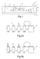
Figure 1 is a cross-section of an embodiment of the present packaged device; -
Figure 2a shows an enlarged detail ofFigure 1 ; -
Figure 2b shows a variant of the enlarged detail ofFigure 2a ; -
Figure 3 is a cross-section of another embodiment of the present packaged device; -
Figure 4 shows a perspective and enlarged view of a detail of a different embodiment of the package; -
Figure 5 is a top plan view of the detail ofFigure 4 ; -
Figure 6 shows the repellent behaviour of the package ofFigure 4 ; -
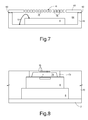
Figure 7 is a cross-section of a different embodiment of the present packaged device; and -
Figures 8-10 show other embodiments of the present device. - In
Figure 1 , a packageddevice 1 comprises abase 2 and acap 3. Thecap 3 is here half-shell shaped, generally parallelepipedal, including atop wall 3a and aside wall 3b and is fixed, typically glued, to thebase 2, so as to form a package. Theprotective cap 3 and thebase 2 form a package surrounding achamber 4. In the embodiment ofFigure 1 , anintegrated circuit 5 is fixed on thebase 2 within thechamber 4, for example glued, and achip 6 is fixed on the integratedcircuit 5, for example glued. Alternatively, both theintegrated circuit 5 and thechip 6 could be fixed to thebase 2, adjacent to each other. Thetop wall 3a has anouter surface 9. - For example, the
base 2 may be formed by a single-layer or multi-layer organic substrate, of epoxy resin, such as a laminate of BT (bismaleimide triazine) or FR-4 or any other similar material for printed circuits, or by a ceramic substrate and has a parallelepipedal plate shape. - The
cap 3 may be, for example, of silicon, metal, ceramic, Teflon or other plastic material, in particular polymeric, for instance a material similar to the one used for manufacturing the core of FR-4 or BT substrates. - The
chip 6 forms a MEMS (microelectromechanical system), for example, a pressure sensor. In this case, thechip 6 may have amembrane 7 delimited by a buriedcavity 8. Theintegrated circuit 5 may form a signal-processing circuit of thechip 4, for example a reading circuit formed as an ASIC (Application-Specific Integrated Circuit) for amplifying and treating the signal supplied by thechip 6. Conductive wires 10 connect thechip 6 to theintegrated circuit 5 andconductive wires 11 connect theintegrated circuit 5 to conductive areas (typically contact pads and connection lines not shown, on the surface and/or integrated in the substrate 2), for exchanging electrical signals and power supplies, in a per se known manner. - The
cap 3 comprises apermeable area 17 arranged preferably over thechip 6 and carrying a liquid-repellent, hydrophobic, oleophobic, or lipophobic structure. A plurality ofholes 15 is formed in thepermeable area 17. - In the embodiment of
Figure 1 , the liquid-repellent structure is formed by arough nanostructure 16 defined by theouter surface 9 of thetop wall 3a of thecap 3, as shown in the enlarged detail ofFigures 2a and 2b . - In
Figure 2a , theouter surface 9 hasmicroreliefs 20 having geometrical characteristics such as to impart on the outer surface 9 a desired roughness. Here, themicroreliefs 20 are formed by pillars with circular, square, or polyhedral, base that are frustoconical, parallelepipedal, frustopyramidal, or the like. For example, the microreliefs orpillars 20 may have a base side or diameter comprised between 0.5 and 20 µm, a height comprised between 1 and 50 µm and be arranged at a mutual distance (pitch) comprised between 2 and 150 µm. Themicroreliefs 20 may be distributed differently, for example have a greater width so that asingle microrelief 20 is arranged between a pair of adjacent holes 15 (similarly to what shown inFigures 4 and9 , as described in greater detail hereinafter). Theholes 15 may have any shape, for example circular, quadrangular, polygonal, whether regular or irregular and be made before or after forming therough nanostructure 16, for example, by masked chemical etching, in a known manner. Alternatively, theholes 15 may be formed by laser drilling. - For example, with a
top surface 3a of thecap 3 having a thickness comprised between 20 and 100 µm in the area of theholes 15, these may have a width comprised between 0.1 and 100 µm and be arranged at a mutual distance comprised between 0.3 and 300 µm, with a width-to-pitch ratio of, for example, at least 1:3. However, in case ofsingle microreliefs 20 between two adjacent holes 15 (Figures 4 and9 ), the width-to-distance ratio may be also equal to or greater than 1. - In
Figure 2b , therough nanostructure 16 is irregular and the microreliefs 20' typically differ in shape, arrangement, base area, height and other geometrical characteristics. Theholes 15 may have the dimensions indicated above. - In either case, for example, the
rough nanostructure 16 may have a value Ra (defined as arithmetic average value of the deviations in absolute value of the actual profile of the surface with respect to the mean line) comprised between 0.5 and 3 µm, Rmax (defined as maximum deviation, i.e., distance between the highest peak and the lowest point of the surface 9) comprised between 2 and 20 µm. - The
rough nanostructure 16 ofFigure 2a may be formed via nanolithography on silicon. - Instead, the irregular
rough nanostructure 16 ofFigure 2b may be formed by chemical etching. If thecap 3 is of metal, the chemical etching may be performed with hydrofluoric acid. - Alternatively, the
rough nanostructure 16 ofFigure 2b may also be formed by laser irradiation of thecap 3 if made of silicon, or hot embossing or laser irradiation of thecap 3 if it is made of plastic material. - By varying the level of laser irradiation, it is possible to modify the roughness and thus the wettability of the
top surface 3a of thesilicon cap 3 so as to increase the value of the contact angle beyond 90°. - After forming the
rough nanostructure 16, theprotective cap 3 is fixed to thebase 2 where theintegrated circuit 5 and thechip 6 have been already fixed, so that thechamber 4 surrounds them. - The hydrophobicity of rough silicon surfaces has been reported in numerous studies; see, for example, "Making silicon hydrophobic: wettability control by two-length scale simultaneous patterning with femtosecond laser irradiation", V. Zorba et al., 2 Nanotechnology 17 (2006) 3234-3238, IP address for downloading: 77.242.201.53.
- In this way, the
holes 15 enable environmental air to enter thechamber 4 but therough nanostructure 16 prevents droplets of water or other liquids from penetrating into thechamber 4 through theholes 15, as shown in the detail ofFigures 2a and 2b . Consequently, thechip 6 is able to work properly, for example measuring the atmospheric pressure, without being damaged by external humidity, water, or other liquids in which the packageddevice 1 were to be dropped. - In
Figure 3 , the liquid-repellent structure is formed by a hydrophobic/lipophobic liquid-repellent layer 30, which extends over thecap 33, at least on top of the area of theholes 15. In the example shown, the liquid-repellent layer 30 coats the outer surface of theentire cap 33. - The liquid-
repellent layer 30 may be a layer of a material chosen from among Teflon, silicon carbide, resist such as SU-8 (see, for example: "The use of high aspect ratio photoresist (SU-8) for super-hydrophobic pattern prototyping", Neil J. Shirtcliffe et al., JOURNAL OF MICROMECHANICS AND MICROENGINEERING, J. Micromech. Microeng. 14 (2004) 1384-1389, IP address for downloading: 77.242.201.53), polymers (see, for example: "Ultrahydrophobic Polymer Surfaces Prepared by Simultaneous Ablation of Polypropylene and Sputtering of Poly(tetrafluoroethylene) Using Radio Frequency Plasma", Jeffrey P. Youngblood et al., Macromolecules 1999, 32, 6800-6806, 1999 American Chemical Society), organometals, or transition-metal complexes, such as the materials produced by Aculon. - The liquid-
repellent layer 30 may be formed by dipping theprotective cap 33 in an appropriate solution or by mechanical deposition via spinning or by thermochemical deposition. Alternatively, the material of the liquid-repellent layer 30 may be the material described in the patent application "Process for manufacturing a microdevice having regions with different wettability and corresponding microdevice" filed on the same date by the present applicant, the material being obtained by arranging thecap 3 in a plasma of C4F8 precursor gas in an apparatus for reactive-ion-etching processes so as to obtain a C4F8 polymer having a static contact angle greater than 100°, with spectral absorption peak at a wave number comprised between 1200 cm-1 and 1300 cm-1, in particular 1250 cm-1. - After coating the
cap 33 with the liquid-repellent layer 30, theholes 15 are formed using the techniques indicated above (chemical etching and/or laser drilling). -
Figures 4 and5 show a detail of an embodiment where therough nanostructure 16 is formed by a plurality ofpillars 50, of silicon, formed on theouter surface 9, projecting from thetop wall 3a and monolithical with thecap 3. Thepillars 50 here have a reduced width as compared to the distance between twoadjacent holes 15 and may have a more or less squared shape. - In addition, in the example shown, the
pillars 50 are covered bycaps 53 belonging to a hydrophobic/lipophobic layer 54, for example, a metal or non-metal layer such as Teflon. The hydrophobic/lipophobic layer 54 has openings 55 (see, in particular,Figure 5 ) above theholes 15 so as to enable passage of air through theopenings 55 and theholes 15, as far as the underlying chamber 4 (not visible inFigures 4 and5 ). - Here, the
holes 15 may be arranged at a maximum distance from each other comprised between 300 nm and 20 µm, for example 400 nm, have a maximum width comprised between 50 nm and 10 µm, for example 60 nm, and thepillars 50 may have a width comprised between 150 nm and 15 µm, for example 200 nm. The hydrophobic/lipophobic layer 54 may have a thickness comprised between 100 nm and 1 µm, for example 300 nm. - In
Figure 6 , therough nanostructure 16 on theouter surface 9 of thecap 3 is formed by spheroidal structures that resemble thepillars 50. As may be noted, the rough nanostructure 16 (pillars 50) and the hydrophobic/lipophobic layer 54 form also here a liquid-repellent structure 56 that prevents entry of liquids into theholes 15. In practice, due to surface tension of the liquids, the liquid-repellent structure 56 does not allow aliquid drop 57 to wet its entire surface, but air pockets are formed underneath the drops and prevent the latter from entering theholes 15. -
Figure 7 shows an embodiment where thecap 63 is formed by a plane wall and is bonded viaadhesive portions 60 to a base 62 half-shell shaped, generally parallelepipedal, which defines, together with theprotective cap 63, thechamber 4. Here, thechip 6 is directly bonded to thebase 62. As inFigure 1 , thecap 63 hasholes 15 and arough nanostructure 16 such as to enable entry of air but not of liquids, thanks to its hydrophobic or lipophobic structure. -
Figure 8 shows an embodiment where thecap 73 is fixed to the top of thechip 6 and thus thechamber 74 does not surround the latter but only the membrane 77 (sensitive area of thechip 6;cap 73 made at a chip-scale level). Here, a moldedregion 70 laterally surrounds thecap 73, thechip 6 and theintegrated circuit 5, laterally aligned to thebase 2 and at the top to thecap 73. The moldedregion 70 is, for example, of plastic material and may comprise resin. - The
cap 73 also here has a liquid-repellent structure, made according to what shown inFigures 1-6 . - In
Figure 9 , thecap 73 is directly fixed to thechip 6, similarly toFigure 8 , but thechip 6 is directly fixed to thebase 2 and has suitable throughconnections 80. Here, the moldedregion 70 is missing and the liquid-repellent structure 56 is formed bynon-coated pillars 50, as highlighted in the enlarged detail. Alternatively, also in this case thepillars 50 may be coated with a hydrophobic/lipophobic layer, such as thelayer 54 ofFigures 4-5 or may be replaced by therough nanostructure 16 ofFigure 6 , with spheroidal structures. - In
Figure 10 , thecap 73 is once again directly fixed to thechip 6, but the electrical connection between thechip 6 and thebase 2 occurs viacontact pads 81 andwire 82, in a known way. Here, the moldedregion 70 is present. - Obviously, other intermediate combinations are possible and the liquid-
repellent structure 56 may be made in any way described above with reference toFigures 1-9 . - Finally, it is clear that modifications and variations may be made to the packaged device described and illustrated herein, without thereby departing from the scope of the present invention, as defined in the attached claims.
- For example, in the embodiment of
Figures 4-6 , the pillars may have head portions of different shape, for example hemispherical or irregular, so as to form a non-plane top surface.
Claims (16)
- A packaged device, comprising a chip (6) and a package (3, 2; 33; 62, 63; 70, 73) delimiting a chamber (4; 64; 74) surrounding at least one sensitive portion (7) of the chip and provided with an air-permeable area (17) having a plurality of holes (15) and a liquid-repellent structure (16; 30; 56) so as to enable passage of air between an external environment and the chamber and block passage of liquids.
- The packaged device according to claim 1, wherein the holes (15) have a maximum width comprised between 0.1 and 100 µm and are arranged at a distance from each other (pitch) comprised between 0.3 and 300 µm, with a width-to-pitch ratio of at least 1:3.
- The packaged device according to claim 1 or 2, wherein the package comprises a protective cap (7; 33; 63; 73) delimiting un upper portion of the chamber (4; 64; 74) and defining an outer surface (9).
- The packaged device according to claim 3, wherein the liquid-repellent structure comprises a rough nanostructure (16) formed by the outer surface (9) of the protective cap (7; 63; 73) at least at the air-permeable area (17) and has a plurality of microreliefs (20, 20').
- The packaged device according to claim 4, wherein the rough nanostructure (16), at the air-permeable area (17), has a roughness value comprised between 1 and 3 µm and a maximum deviation comprised between 2 and 20 µm.
- The packaged device according to claim 4 or 5, wherein the microreliefs (20; 50) have a regular structure and are uniformly arranged on the outer surface (9) or have irregular conformation and arrangement (20').
- The packaged device according to any of claims 3-6, wherein the liquid-repellent structure comprises a hydrophobic/lipophobic layer (30; 53), which covers the protective cap (3; 33; 73), at least in the air-permeable area (17) and is provided with openings (55) overlying the holes (15).
- The packaged device claim 7, wherein the hydrophobic/lipophobic layer (30; 53) is made of a material including one of Teflon, silicon carbide, resist such as SU-8, metal, polymer, such as a C4F8 polymer having a static contact angle greater than 100°, a spectral absorption peak at a wave number comprised between 1200 cm-1 and 1300 cm-1, organometal and transition-metal complex.
- The packaged device according to any of claims 3-8, wherein the protective cap (7; 63; 73) is made of a material including one of silicon, metal, plastic material, such as a polymer and Teflon, ceramic.
- The packaged device according to any of the preceding claims, wherein the chip (6) integrates a MEMS, in particular a pressure sensor, and an upper surface of the MEMS is located in the chamber.
- A method for manufacturing a packaged device, comprising the steps of:forming a package (3, 2; 33; 62, 63; 70, 73) delimiting a chamber (4; 64; 74);enclosing at least one portion of a chip (6) in the package so that the chamber surrounds at least one sensitive portion (7) of the chip;forming an air-permeable area (17) in the package including forming a plurality of holes (15); andforming a liquid-repellent structure (16; 30; 56) on the air-permeable area.
- The method according to claim 11, wherein the step of forming a liquid-repellent structure comprises providing a rough structure (16) having microreliefs (20; 20'; 50) on an outer surface (9) of the air-permeable area (17), for example by chemical etching or nanolithography.
- The method according to claim 11 or 12, wherein the step of forming a liquid-repellent structure comprises forming a hydrophobic/lipophobic layer (30; 53) on top of the outer surface (9) of the air-permeable area (17).
- The method according to claim 13, wherein the step of forming a package comprises providing a protective cap (7; 33; 63; 73) over the sensitive portion of the cap.
- The method according to claim 14, wherein the step of forming a hydrophobic/lipophobic layer (30; 53) comprises dipping the protective cap (33) in a solution or depositing via spinning material having hydrophobic/lipophobic characteristics.
- The method according to any of claims 11-15, wherein forming a plurality of holes (15) is carried out before or after forming a liquid-repellent structure.
Applications Claiming Priority (1)
| Application Number | Priority Date | Filing Date | Title |
|---|---|---|---|
| IT000753A ITTO20120753A1 (en) | 2012-08-30 | 2012-08-30 | ENCAPSULATED DEVICE EXPOSED TO AIR, ENVIRONMENT AND LIQUIDS AND RELATIVE PROCESS OF MANUFACTURE |
Publications (1)
| Publication Number | Publication Date |
|---|---|
| EP2703338A1 true EP2703338A1 (en) | 2014-03-05 |
Family
ID=47018387
Family Applications (1)
| Application Number | Title | Priority Date | Filing Date |
|---|---|---|---|
| EP20130182526 Withdrawn EP2703338A1 (en) | 2012-08-30 | 2013-08-30 | Packaged device designed to be exposed to environmental air and liquids and manufacturing method thereof |
Country Status (4)
| Country | Link |
|---|---|
| US (1) | US9011776B2 (en) |
| EP (1) | EP2703338A1 (en) |
| CN (2) | CN103663346B (en) |
| IT (1) | ITTO20120753A1 (en) |
Cited By (3)
| Publication number | Priority date | Publication date | Assignee | Title |
|---|---|---|---|---|
| WO2017055806A1 (en) * | 2015-09-30 | 2017-04-06 | Cambridge Cmos Sensors Limited | Gas sensor with a gas permeable region |
| WO2018197836A1 (en) * | 2017-04-28 | 2018-11-01 | Cirrus Logic International Semiconductor Limited | Mems device and process |
| WO2019011748A1 (en) * | 2017-07-10 | 2019-01-17 | Tdk Electronics Ag | Mems device with particle filter and method of manufacture |
Families Citing this family (25)
| Publication number | Priority date | Publication date | Assignee | Title |
|---|---|---|---|---|
| ITTO20120753A1 (en) * | 2012-08-30 | 2014-03-01 | St Microelectronics Srl | ENCAPSULATED DEVICE EXPOSED TO AIR, ENVIRONMENT AND LIQUIDS AND RELATIVE PROCESS OF MANUFACTURE |
| US9962084B2 (en) * | 2013-06-15 | 2018-05-08 | Purdue Research Foundation | Wireless interstitial fluid pressure sensor |
| US9491531B2 (en) * | 2014-08-11 | 2016-11-08 | 3R Semiconductor Technology Inc. | Microphone device for reducing noise coupling effect |
| CN105181230A (en) * | 2015-08-06 | 2015-12-23 | 苏州敏芯微电子技术有限公司 | Pressure sensor and packaging method thereof |
| US10562761B2 (en) | 2015-11-18 | 2020-02-18 | Kathirgamasundaram Sooriakumar | Waterproof microphone and associated packing techniques |
| JP2017146101A (en) | 2016-02-15 | 2017-08-24 | セイコーエプソン株式会社 | Waterproof member, method for manufacturing waterproof member, pressure sensor, and electronic module |
| JP6667351B2 (en) * | 2016-04-08 | 2020-03-18 | アルプスアルパイン株式会社 | Sensor device |
| US10483191B2 (en) * | 2016-07-15 | 2019-11-19 | Stmicroelectronics, Inc. | Bottom package exposed die MEMS pressure sensor integrated circuit package design |
| DE102017200162A1 (en) * | 2017-01-09 | 2018-07-12 | Robert Bosch Gmbh | Method for producing a microelectromechanical component and wafer arrangement |
| US10231061B2 (en) * | 2017-04-28 | 2019-03-12 | Infineon Technologies Ag | Sound transducer with housing and MEMS structure |
| GB2563461B (en) * | 2017-06-16 | 2021-11-10 | Cirrus Logic Int Semiconductor Ltd | Transducer packaging |
| DE102017211451B4 (en) * | 2017-07-05 | 2019-03-21 | Robert Bosch Gmbh | Micromechanical sensor device and corresponding manufacturing method |
| US10640367B2 (en) * | 2017-09-29 | 2020-05-05 | Apple Inc. | Water proofing and water detection schemes for MEMS-based environmental sensing devices |
| EP3480589B1 (en) * | 2017-11-03 | 2022-09-21 | Honeywell International Inc. | Electrochemical gas sensor constructed with mems fabrication technology |
| DE102017220258B4 (en) * | 2017-11-14 | 2023-11-30 | Infineon Technologies Ag | Semiconductor sensor device and method for producing the same |
| CN112262101A (en) * | 2018-04-09 | 2021-01-22 | 应美盛股份有限公司 | Environmentally friendly sensing device |
| DE102018207548B3 (en) | 2018-05-16 | 2019-06-19 | Robert Bosch Gmbh | Sensor device with a hydrophobic and / or anti-adhesive protective layer and method for producing such a sensor device |
| CN109030563B (en) * | 2018-05-29 | 2021-07-02 | 苏州慧闻纳米科技有限公司 | Gas sensor and preparation method thereof |
| DE102018123023A1 (en) * | 2018-09-19 | 2020-03-19 | Tdk Electronics Ag | Membrane, pressure sensor system and method for manufacturing the pressure sensor system |
| DE102018129058A1 (en) * | 2018-11-19 | 2020-05-20 | Bundesanstalt für Materialforschung und -Prüfung (BAM) | Sensor device and method for producing a sensor device |
| US20210246015A1 (en) * | 2020-02-06 | 2021-08-12 | Advanced Semiconductor Engineering, Inc. | Sensor device package and method for manufacturing the same |
| US11945714B2 (en) * | 2020-07-30 | 2024-04-02 | Stmicroelectronics S.R.L. | Electronic device and corresponding method |
| WO2024075462A1 (en) * | 2022-10-03 | 2024-04-11 | ローム株式会社 | Pressure sensor |
| EP4408016A1 (en) * | 2023-01-27 | 2024-07-31 | Infineon Technologies AG | Mems device with membrane comprising upright nanostructures and method for manufacturing same |
| DE102023211885A1 (en) * | 2023-11-28 | 2025-05-28 | Robert Bosch Gesellschaft mit beschränkter Haftung | Microelectromechanical sensor and method for producing a microelectromechanical sensor |
Citations (3)
| Publication number | Priority date | Publication date | Assignee | Title |
|---|---|---|---|---|
| US3963881A (en) * | 1973-05-29 | 1976-06-15 | Thermo Electron Corporation | Unidirectional condenser microphone |
| US20020181725A1 (en) * | 2001-05-31 | 2002-12-05 | Ib Johannsen | Method of providing a hydrophobic layer and a condenser microphone having such a layer |
| WO2009116957A2 (en) * | 2008-03-19 | 2009-09-24 | Sensfab Pte Ltd | Water resistant ultra-low pressure sensor |
Family Cites Families (11)
| Publication number | Priority date | Publication date | Assignee | Title |
|---|---|---|---|---|
| GB2199541A (en) | 1986-10-16 | 1988-07-13 | Rig Design Services | Production of engineering drawings |
| DE69937774T2 (en) | 1998-08-19 | 2008-12-04 | NGK Spark Plug Co., Ltd., Nagoya-shi | gas sensor |
| US6165905A (en) | 1999-01-20 | 2000-12-26 | Philips Electronics, North America Corp. | Methods for making reliable via structures having hydrophobic inner wall surfaces |
| CA2563406C (en) * | 2004-04-23 | 2013-09-17 | Research Triangle Institute | Flexible electrostatic actuator |
| JPWO2005123242A1 (en) * | 2004-06-15 | 2008-07-31 | 日本電気株式会社 | Structure, chip using the same, and lyophilic/lyophobic control method |
| KR100687570B1 (en) | 2005-07-19 | 2007-02-27 | 삼성전기주식회사 | Nozzle for Inkjet Head and Manufacturing Method Thereof |
| JP2010000464A (en) * | 2008-06-20 | 2010-01-07 | Japan Gore Tex Inc | Vent filter and method for manufacturing thereof |
| US8518320B2 (en) | 2009-05-21 | 2013-08-27 | University Of Cincinnati | Methods for electrospinning hydrophobic coaxial fibers into superhydrophobic and oleophobic coaxial fiber mats |
| FR2946658B1 (en) | 2009-06-11 | 2011-08-05 | Commissariat Energie Atomique | MICROFLUIDIC DEVICE COMPRISING TWO HYDROPHOBIC LAYERS ASSEMBLED TO ONE ANOTHER AND METHOD OF ASSEMBLY |
| CN102081335B (en) * | 2010-11-18 | 2012-07-25 | 北京航空航天大学 | Liquid patterned device for photoelectric synergic induced anisotropic infiltration and manufacturing method |
| ITTO20120753A1 (en) * | 2012-08-30 | 2014-03-01 | St Microelectronics Srl | ENCAPSULATED DEVICE EXPOSED TO AIR, ENVIRONMENT AND LIQUIDS AND RELATIVE PROCESS OF MANUFACTURE |
-
2012
- 2012-08-30 IT IT000753A patent/ITTO20120753A1/en unknown
-
2013
- 2013-08-16 CN CN201310361495.6A patent/CN103663346B/en active Active
- 2013-08-16 CN CN201320509477.3U patent/CN203667994U/en not_active Withdrawn - After Issue
- 2013-08-29 US US14/013,730 patent/US9011776B2/en active Active
- 2013-08-30 EP EP20130182526 patent/EP2703338A1/en not_active Withdrawn
Patent Citations (3)
| Publication number | Priority date | Publication date | Assignee | Title |
|---|---|---|---|---|
| US3963881A (en) * | 1973-05-29 | 1976-06-15 | Thermo Electron Corporation | Unidirectional condenser microphone |
| US20020181725A1 (en) * | 2001-05-31 | 2002-12-05 | Ib Johannsen | Method of providing a hydrophobic layer and a condenser microphone having such a layer |
| WO2009116957A2 (en) * | 2008-03-19 | 2009-09-24 | Sensfab Pte Ltd | Water resistant ultra-low pressure sensor |
Non-Patent Citations (2)
| Title |
|---|
| JEFFREY P. YOUNGBLOOD ET AL.: "Macromolecules", vol. 32, 1999, AMERICAN CHEMICAL SOCIETY, article "Ultrahydrophobic Polymer Surfaces Prepared by Simultaneous Ablation of Polypropylene and Sputtering of Poly(tetrafluoroethylene) Using Radio Frequency Plasma", pages: 6800 - 6806 |
| SHIRTCLIFFE ET AL.: "JOURNAL OF MICROMECHANICS AND MICROENGINEERING", J. MICROMECH. MICROENG, vol. 14, 2004, pages 1384 - 1389 |
Cited By (7)
| Publication number | Priority date | Publication date | Assignee | Title |
|---|---|---|---|---|
| WO2017055806A1 (en) * | 2015-09-30 | 2017-04-06 | Cambridge Cmos Sensors Limited | Gas sensor with a gas permeable region |
| US20180202958A1 (en) * | 2015-09-30 | 2018-07-19 | Ams Sensors Uk Limited | Gas sensor with a gas permeable region |
| US11022576B2 (en) | 2015-09-30 | 2021-06-01 | Sciosense B.V. | Gas sensor with a gas permeable region |
| WO2018197836A1 (en) * | 2017-04-28 | 2018-11-01 | Cirrus Logic International Semiconductor Limited | Mems device and process |
| US11337010B2 (en) | 2017-04-28 | 2022-05-17 | Cirrus Logic, Inc. | MEMS device and process |
| WO2019011748A1 (en) * | 2017-07-10 | 2019-01-17 | Tdk Electronics Ag | Mems device with particle filter and method of manufacture |
| US11787689B2 (en) | 2017-07-10 | 2023-10-17 | Tdk Corporation | MEMS device with particle filter and method of manufacture |
Also Published As
| Publication number | Publication date |
|---|---|
| US9011776B2 (en) | 2015-04-21 |
| ITTO20120753A1 (en) | 2014-03-01 |
| US20140061892A1 (en) | 2014-03-06 |
| CN103663346B (en) | 2017-04-12 |
| CN103663346A (en) | 2014-03-26 |
| CN203667994U (en) | 2014-06-25 |
Similar Documents
| Publication | Publication Date | Title |
|---|---|---|
| US9011776B2 (en) | Packaged device exposed to environmental air and liquids and manufacturing method thereof | |
| EP2121513B1 (en) | Electronic device comprising differential sensor mems devices and drilled substrates | |
| US8546895B2 (en) | Electronic device including MEMS devices and holed substrates, in particular of the LGA or BGA type | |
| USRE46671E1 (en) | Substrate-level assembly for an integrated device, manufacturing process thereof and related integrated device | |
| EP3429957B1 (en) | Component carrier with integrated wall structure for subsequent assembly of an electronic component | |
| US9708174B2 (en) | Process for manufacturing a packaged device, in particular a packaged micro-electro-mechanical sensor, having an accessible structure, such as a MEMS microphone and packaged device obtained thereby | |
| US9434606B2 (en) | Micromechanical inertial sensor and method for manufacturing same | |
| CN104249990B (en) | MEMS device and its manufacturing process comprising fluid path | |
| KR101622864B1 (en) | Venting array and manufacturing method | |
| KR20150105240A (en) | Sensor structure for sensing pressure waves and ambient pressure | |
| US10281442B2 (en) | Sensor device | |
| EP3456682B1 (en) | Sensor system, sensor arrangement, and assembly method using solder for sealing | |
| KR102437764B1 (en) | Sensor package, Method of manufacturing sensor package, and Method of manufacturing lid structure | |
| KR102313151B1 (en) | Method for Fabricating Stress Decoupled Micromechanical Pressure Sensors | |
| CN108622845B (en) | Semiconductor device packaging and manufacturing method | |
| US20210114866A1 (en) | Mems device with particle filter and method of manufacture | |
| CN106057777A (en) | Semiconductor device including a cavity lid | |
| US10676344B2 (en) | Protective environmental barrier for a die | |
| EP1717562A1 (en) | A method for packaging integrated sensors | |
| KR101060121B1 (en) | Semiconductor package for vertical and horizontal mounting and manufacturing method | |
| EP3339243B1 (en) | Interconnected layer stack with vertically aligned mems and assigned chip | |
| JP2015137937A (en) | Humidity sensor and method for manufacturing the same | |
| US20250290886A1 (en) | Gas sensor package structure | |
| TW202537055A (en) | Gas sensor package structure |
Legal Events
| Date | Code | Title | Description |
|---|---|---|---|
| AK | Designated contracting states |
Kind code of ref document: A1 Designated state(s): AL AT BE BG CH CY CZ DE DK EE ES FI FR GB GR HR HU IE IS IT LI LT LU LV MC MK MT NL NO PL PT RO RS SE SI SK SM TR |
|
| AX | Request for extension of the european patent |
Extension state: BA ME |
|
| PUAI | Public reference made under article 153(3) epc to a published international application that has entered the european phase |
Free format text: ORIGINAL CODE: 0009012 |
|
| STAA | Information on the status of an ep patent application or granted ep patent |
Free format text: STATUS: THE APPLICATION IS DEEMED TO BE WITHDRAWN |
|
| 18D | Application deemed to be withdrawn |
Effective date: 20140906 |