EP2696249A1 - Processor Connectivity - Google Patents
Processor Connectivity Download PDFInfo
- Publication number
- EP2696249A1 EP2696249A1 EP13187276.4A EP13187276A EP2696249A1 EP 2696249 A1 EP2696249 A1 EP 2696249A1 EP 13187276 A EP13187276 A EP 13187276A EP 2696249 A1 EP2696249 A1 EP 2696249A1
- Authority
- EP
- European Patent Office
- Prior art keywords
- processor
- replicated
- processing modules
- processing module
- modules
- Prior art date
- Legal status (The legal status is an assumption and is not a legal conclusion. Google has not performed a legal analysis and makes no representation as to the accuracy of the status listed.)
- Granted
Links
Images




Classifications
-
- G—PHYSICS
- G05—CONTROLLING; REGULATING
- G05B—CONTROL OR REGULATING SYSTEMS IN GENERAL; FUNCTIONAL ELEMENTS OF SUCH SYSTEMS; MONITORING OR TESTING ARRANGEMENTS FOR SUCH SYSTEMS OR ELEMENTS
- G05B19/00—Program-control systems
- G05B19/02—Program-control systems electric
- G05B19/04—Program control other than numerical control, i.e. in sequence controllers or logic controllers
- G05B19/042—Program control other than numerical control, i.e. in sequence controllers or logic controllers using digital processors
- G05B19/0428—Safety, monitoring
-
- G—PHYSICS
- G06—COMPUTING OR CALCULATING; COUNTING
- G06F—ELECTRIC DIGITAL DATA PROCESSING
- G06F11/00—Error detection; Error correction; Monitoring
- G06F11/07—Responding to the occurrence of a fault, e.g. fault tolerance
- G06F11/0703—Error or fault processing not based on redundancy, i.e. by taking additional measures to deal with the error or fault not making use of redundancy in operation, in hardware, or in data representation
- G06F11/0751—Error or fault detection not based on redundancy
- G06F11/0754—Error or fault detection not based on redundancy by exceeding limits
- G06F11/0757—Error or fault detection not based on redundancy by exceeding limits by exceeding a time limit, i.e. time-out, e.g. watchdogs
-
- G—PHYSICS
- G06—COMPUTING OR CALCULATING; COUNTING
- G06F—ELECTRIC DIGITAL DATA PROCESSING
- G06F11/00—Error detection; Error correction; Monitoring
- G06F11/07—Responding to the occurrence of a fault, e.g. fault tolerance
- G06F11/16—Error detection or correction of the data by redundancy in hardware
- G06F11/18—Error detection or correction of the data by redundancy in hardware using passive fault-masking of the redundant circuits
-
- G—PHYSICS
- G05—CONTROLLING; REGULATING
- G05B—CONTROL OR REGULATING SYSTEMS IN GENERAL; FUNCTIONAL ELEMENTS OF SUCH SYSTEMS; MONITORING OR TESTING ARRANGEMENTS FOR SUCH SYSTEMS OR ELEMENTS
- G05B2219/00—Program-control systems
- G05B2219/20—Pc systems
- G05B2219/21—Pc I-O input output
- G05B2219/21056—Decoding on module, module can be inserted anywhere, fixed address in bus connector
-
- G—PHYSICS
- G05—CONTROLLING; REGULATING
- G05B—CONTROL OR REGULATING SYSTEMS IN GENERAL; FUNCTIONAL ELEMENTS OF SUCH SYSTEMS; MONITORING OR TESTING ARRANGEMENTS FOR SUCH SYSTEMS OR ELEMENTS
- G05B2219/00—Program-control systems
- G05B2219/20—Pc systems
- G05B2219/24—Pc safety
- G05B2219/24181—Fail silent nodes, replicated nodes grouped into fault tolerant units
-
- G—PHYSICS
- G05—CONTROLLING; REGULATING
- G05B—CONTROL OR REGULATING SYSTEMS IN GENERAL; FUNCTIONAL ELEMENTS OF SUCH SYSTEMS; MONITORING OR TESTING ARRANGEMENTS FOR SUCH SYSTEMS OR ELEMENTS
- G05B2219/00—Program-control systems
- G05B2219/20—Pc systems
- G05B2219/25—Pc structure of the system
- G05B2219/25174—Ethernet
-
- G—PHYSICS
- G05—CONTROLLING; REGULATING
- G05B—CONTROL OR REGULATING SYSTEMS IN GENERAL; FUNCTIONAL ELEMENTS OF SUCH SYSTEMS; MONITORING OR TESTING ARRANGEMENTS FOR SUCH SYSTEMS OR ELEMENTS
- G05B2219/00—Program-control systems
- G05B2219/20—Pc systems
- G05B2219/25—Pc structure of the system
- G05B2219/25469—Inserting or taking out circuit boards during power on
Definitions
- This invention relates to processor connectivity, in particular in an Industrial Process Control System suitable for:
- control systems are applicable to many industries including oil and gas production and refining, chemical production and processing, power generation, paper and textile mills and sewage treatment plants.
- fault tolerance is of utmost importance. Fault tolerance is the ability to continue functioning safely in the event of one or more failures within the system.
- Fault tolerance may be achieved by a number of different techniques, each with its specific advantages and disadvantages
- TMR Triple Modular Redundancy
- critical circuits are triplicated and perform identical functions simultaneously and independently.
- the data output from each of the three circuits is voted in a majority-voting circuit, before affecting the system's outputs. If one of the triplicated circuits fails, its data output is ignored. However, the system continues to output to the process the value (voltage, current level, or discrete output state) that agrees with the majority of the functional circuits.
- TMR provides continuous, predictable operation.
- TMR systems are expensive to implement if full TMR is not actually a requirement, and it is desirable to utilise an architecture which provides flexibility so that differing levels of fault tolerance can be provided depending upon specified system requirements.
- Another approach to fault tolerance is the use of hot-standby modules. This approach provides a level of fault tolerance whereby the standby module maintains system operation in the event of module failure. With this approach there may be some disruption to system operation during the changeover period if the modules are not themselves fault-tolerant.
- Fault tolerant systems ideally create a Fault Containment Region (FCR) to ensure that a fault within the FCR boundary does not propagate to the remainder of the system. This enables multiple faults to co-exist on different parts of a system without affecting operation.
- FCR Fault Containment Region
- Fault tolerant systems generally employ dedicated hardware and software test and diagnostic regimes that provide very fast fault recognition and response times to provide a safer system.
- Safety control systems are generally designed to be 'fail-operational/fail-safe'. Fail operational means that when a failure occurs, the system continues to operate: it is in a fail-operational state. The system should continue to operate in this state until the failed module is replaced and the system is returned to a fully operational state.
- An example of fail safe operation occurs, for example if, in a TMR system, a failed module is not replaced before a second failure in a parallel circuit occurs, the second failure should cause the TMR system to shut down to a fail-safe state. It is worth noting that a TMR system can still be considered safe, even if the second failure is not failsafe, as long as the first fault is detected and communicated, and is itself failsafe.
- This invention provides a technique whereby replicated processor modules can be connected together in a simpler way than is provided for by conventional physical layer circuitry.
- PHY physical layer circuitry
- This invention provides an alternative method of connecting processors which are in close physical proximity to each other.
- the invention also provides an improved connectivity technique whereby processors may be replaced without configuration changes to the system network structure or require manual reconfiguration intervention.
- an apparatus for industrial process control comprising: a plurality of replicated processing modules for receiving replicated sensor input data and for producing replicated output data in which each of said plurality of replicated processing modules is connected to another one of said plurality of replicated processing modules via a dedicated high speed connection.
- each of said plurality of the replicated processing modules is connected to another one of said plurality of replicated processing modules via an RMII interface.
- a processing module comprises a processor having an RMII interface and a buffer, the buffer comprising means for generating a differential signal for transmission from an RMII signal received from said processor.
- a processing module comprises a processor having an RMII interface and a buffer, the buffer comprising means for receiving a differential signal and generating therefrom an RMII signal for sending to said processor.
- a processing module may comprise a processor having an RMII interface and a buffer, the buffer comprising means to clock received data into the buffer in dependence upon a received clock signal and to provide said data to the processor in dependence upon a clock signal generated by said processor.
- the processing modules slot into a backplane, and in which the backplane assembly comprises at least one processor having a store storing network specific information for each of said plurality of replicated processing modules.
- the network specific information may comprise address information.
- a distributed architecture is designed to be used in different SIL (Safety Integrity Level) environments, so that if a high SIL is required it can be provided, but if a low SIL is all that is needed the system can be reduced in complexity in order to reduce unnecessary extra costs.
- SIL Safety Integrity Level
- An exemplary Industrial Process Control System 10 comprises a workstation 12, one or more controllers 14 and a gateway 16.
- the workstation 12 communicates with the controllers 14 and the gateway 16 via Ethernet connections 18 to one or more control networks 13. Multiple Ethernet connections 18 provide redundancy to improve fault tolerance.
- the workstation 12 may be connected via a conventional Ethernet connection 11 to another external network 15.
- a controller 14 will now be described in more detail with reference to Figures 2 and 3 .
- Figure 2 illustrates a schematic diagram of the controller 14 comprising an input assembly 22, a processor assembly 24 and an output assembly 26.
- the input assembly 22 and output assembly 26 are on different backplanes but they may equally well share a single backplane.
- Assemblies 22, 24, 26 are created from one or more communications backplane portions which have three slots to accommodate up to three modules together with termination assemblies which have one, two or three slots, and which interface to field sensors and transducers.
- a termination assembly may straddle two contiguous backplane portions.
- a module comprises a plug in card with multiple connectors for plugging onto a communications backplane and a termination assembly.
- Figure 3 illustrates a possible physical configuration of the controller 14.
- the input assembly 22, output assembly 26 and processor assembly 24 are physically separated from one another by grouping the modules of different types onto separate communications backplanes.
- the input assembly 22 comprises two communications backplane portions, 22', 22".
- the first backplane portion 22' has a triplex input termination assembly and three input modules 22a, 22b, 22c
- the second backplane portion 22" has a duplex input termination assembly 22" and two input modules 22d, 22e.
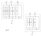
- the processor assembly 24 comprises a single processor backplane portion 24' having three processor modules 24a, 24b and 24c.
- the output assembly 26 comprises two backplane portions 26', 26".
- the first backplane portion 26' has a duplex output termination assembly with two output modules 26a, 26b and the second backplane portion 26" has a simplex output termination assembly with a single output module 26c.
- An input assembly 22 comprises one or more backplane portions and termination assemblies 22' 22" 22"' etc.
- a triplex portion 22' having three modules 22a, 22b, 22c might be used for high availability requirement
- a duplex portion 22" having two modules 22d, 22e might be provided for fault tolerant applications
- a simplex portion 22"' with a single modules 22f might be provided for failsafe applications.
- the termination assemblies may be provided with different types of field conditioning circuits.
- assembly 22' may be provided with a 24V DC field conditioning circuit 41
- assembly 22" may be provided with a 120V DC field conditioning circuit 42
- assembly 22"' may be provided with a 4-20mA field conditioning circuit 43.
- possible configurations are shown for an output assembly 26. It will be appreciated that numerous configurations of backplane portions and termination assemblies with various different numbers of modules and various different types of field conditioning circuits are possible and the invention is not limited to those shown in these examples.
- the processor assembly configures a replacement processor module using data from a parallel module before the replacement module becomes active.
- the field conditioning circuits 41, 42, 43 transform a signal received from a sensor monitoring industrial process control equipment to a desired voltage range, and distribute the signal to the input modules as required.
- Each field conditioning circuit 41, 42, 43 is also connected to field power and field return (or ground) which may be independently isolated on a channel by channel basis from all other grounds, depending on the configuration of the input termination assembly. Independent channel isolation is the preferred configuration because it is the most flexible.
- the field conditioning circuits 41, 42, 43 comprise simple non active parts and are not online replaceable.
- Figure 5 and Figure 6 illustrate the flexibility of the architecture described herein showing different configurations for a triplex system for generating a signal with a high availability requirement.
- a three module input assembly 51 receives a signal from a sensor 50 via a field conditioning circuit in termination assembly 54.
- the field conditioning circuit 54 transforms the signal to a desired voltage range and distributes the signal to three replicated input modules 53a, 53b, 53c.
- Each input module processes the signal and the results are sent to a two out of three voter 52 to generate a result signal in dependence thereon.
- replicated sensors 60a, 60b, 60c each send a signal to respective simplex assemblies 61a, 61b, 61c via respective field conditioning circuits in termination assemblies 64a, 64b, 64c.
- Each input module 63a, 63b, 63c processes the signal and sends an output to a two out of three voter 62 to generate a signal in dependence thereon. It will be appreciated that many variations and configurations are possible in addition to those illustrated here.
- processor modules 24a, 24b, 24c are connected to a processor communications backplane using conventional physical layer circuitry.
- processor modules 24a, 24b, 24c are connected to a processor communications backplane using conventional physical layer circuitry.
- processor modules can be connected together without the need for specialized integrated circuits.
- FIG 7 shows an embodiment of the invention for connecting replicated processor modules in an Industrial Process Control System. In Figure 7 only two processor modules 24a, 24b are shown for clarity.
- the Processor modules utilise the Reduced Media Independent Interface (RMII) connection standard.
- RMII Reduced Media Independent Interface
- Signals used in RMII are as follows: Signal TX_RX_CLK 51 is continuous 50 MHz Reference Clock, signal TXD [1..0] 53 transmits data bits one and zero, signal TX_EN 52 is a transmit enable signal - when high, data on TXD [1..0] 53 will be clocked to the transmitter.
- Signal CRS_DV 54 is a multiplexed carrier sense/ data valid signal which is multiplexed on alternate clock cycles.
- Signal RXD [1..0] 55 receives data bits one and zero.
- the two processor modules 24a, 24b sharing a common backplane 24 are connected together via their serial Ethernet ports (100 Mbit/second) utilizing only very simple field programmable gate array (FPGA) elastic clock domain buffering logic.
- processor 56 is sent and receives RMII signals via an FPGA 57.
- the FPGA 57 in processing module 24a generates differential signals from signals TX_RX_CLK 51, TXD [1..0] 53 and TX_EN 52 using simple logic gates 58 in order to improve signal integrity.
- the signals generated by the FPGA 57 are connected to logic gates 59 in FPGA 57 in processing module 24b.
- Logic gates 59 generate buffer input signals in dependence upon the received differential signals.
- the buffer input signals are clocked into a buffer 60 in dependence upon the received TX_RX_CLK 51 generated by processor module 24a and are clocked out of the buffer in dependence upon TX_RX_CLK 51 internal to processing module 24b. It will be appreciated that signals are transmitted from processing module 24b to processing module 24a in an analogous manner.
- the interconnection scheme using dedicated interconnections provides for high speed data links between multiple processing modules. Connection topology between two processing modules as shown in Figure 7 is straightforward. In an embodiment with three processing modules there are two possible topologies, as illustrated in Figure 8 . Both of these Inter-Processor Link (IPL) methods are provided in the preferred embodiment.
- the first type illustrated in Figure 8a provides point-to-point bidirectional connections between each processor module and the other two, allowing the use of high-speed serial protocols.
- the second type illustrate in Figure 8b provides a broadcast style topology whereby each processor module sends an output which is received by the other two. Provision of a combination of point to point bidirectional connections and broadcast style links may be extended to connect more than three processing module.
- processors 24a, 24b are to be removed from the backplane 24 it is advantageous if this can be done without configuration changes to the system network structure and without requiring manual reconfiguration intervention.
- FIG 9 shows an embodiment of the invention, again showing only two processing modules for clarity.
- Small micro-computer processing elements 82a, 82b resident on the processor backplane 24 store all the network specific information for processing modules, 24a, 24b. This is advantageous over storing such information in the processing modules 24a, 24b themselves. This allows the processing modules 24a, 24b to be replaced without concern for their network parameters.
- the processing modules 24a, 24b are connected via respective sockets 81a, 81b so that they may be easily removed for service independently of the backplane.
- the plurality of storage processors 82a, 82b typically store the media access control (MAC) addresses and internet protocol (IP) addresses that are configured for the processing module.
- Multiple storage processors 82a, 82b may be used to provide fault tolerance.
- processing modules there are three processing modules per node, each of which has unique network parameters. Identical information is stored on each respective storage processor including all information required for each one of the processing modules. This allows any one of the processing modules to be plugged into any one of the backplane sockets. Each processing module is then able to extract information specific to itself.
Landscapes
- Engineering & Computer Science (AREA)
- Theoretical Computer Science (AREA)
- Physics & Mathematics (AREA)
- General Physics & Mathematics (AREA)
- Quality & Reliability (AREA)
- General Engineering & Computer Science (AREA)
- Automation & Control Theory (AREA)
- Hardware Redundancy (AREA)
Abstract
Description
- This invention relates to processor connectivity, in particular in an Industrial Process Control System suitable for:
- Emergency Shutdown systems
- Critical process control systems
- Fire and Gas detection and protection systems
- Rotating machinery control systems
- Burner management systems
- Boiler and furnace control systems
- Distributed monitory and control systems
- Such control systems are applicable to many industries including oil and gas production and refining, chemical production and processing, power generation, paper and textile mills and sewage treatment plants.
- In industrial process control systems, fault tolerance is of utmost importance. Fault tolerance is the ability to continue functioning safely in the event of one or more failures within the system.
- Fault tolerance may be achieved by a number of different techniques, each with its specific advantages and disadvantages
- An example of a system which provides redundancy is a Triple Modular Redundancy (TMR) system. Using TMR, critical circuits are triplicated and perform identical functions simultaneously and independently. The data output from each of the three circuits is voted in a majority-voting circuit, before affecting the system's outputs. If one of the triplicated circuits fails, its data output is ignored. However, the system continues to output to the process the value (voltage, current level, or discrete output state) that agrees with the majority of the functional circuits. TMR provides continuous, predictable operation.
- However, TMR systems are expensive to implement if full TMR is not actually a requirement, and it is desirable to utilise an architecture which provides flexibility so that differing levels of fault tolerance can be provided depending upon specified system requirements.
- Another approach to fault tolerance is the use of hot-standby modules. This approach provides a level of fault tolerance whereby the standby module maintains system operation in the event of module failure. With this approach there may be some disruption to system operation during the changeover period if the modules are not themselves fault-tolerant.
- Fault tolerant systems ideally create a Fault Containment Region (FCR) to ensure that a fault within the FCR boundary does not propagate to the remainder of the system. This enables multiple faults to co-exist on different parts of a system without affecting operation.
- Fault tolerant systems generally employ dedicated hardware and software test and diagnostic regimes that provide very fast fault recognition and response times to provide a safer system.
- Safety control systems are generally designed to be 'fail-operational/fail-safe'. Fail operational means that when a failure occurs, the system continues to operate: it is in a fail-operational state. The system should continue to operate in this state until the failed module is replaced and the system is returned to a fully operational state.
- An example of fail safe operation occurs, for example if, in a TMR system, a failed module is not replaced before a second failure in a parallel circuit occurs, the second failure should cause the TMR system to shut down to a fail-safe state. It is worth noting that a TMR system can still be considered safe, even if the second failure is not failsafe, as long as the first fault is detected and communicated, and is itself failsafe.
- This invention provides a technique whereby replicated processor modules can be connected together in a simpler way than is provided for by conventional physical layer circuitry.
- The problem with conventional physical layer circuitry for connecting Ethernet ports together is that they require a separate integrated circuit known as a "PHY" chip. These chips allow connection of long distance Ethernet communicators, and can be used for short distance connections too. However, use of a PHY chip is expensive, as well as using more power and circuit board area.
- This invention provides an alternative method of connecting processors which are in close physical proximity to each other.
- The invention also provides an improved connectivity technique whereby processors may be replaced without configuration changes to the system network structure or require manual reconfiguration intervention.
- According to the invention there is provided an apparatus for industrial process control comprising: a plurality of replicated processing modules for receiving replicated sensor input data and for producing replicated output data in which each of said plurality of replicated processing modules is connected to another one of said plurality of replicated processing modules via a dedicated high speed connection.
- In a preferred embodiment each of said plurality of the replicated processing modules is connected to another one of said plurality of replicated processing modules via an RMII interface.
- Preferably a processing module comprises a processor having an RMII interface and a buffer, the buffer comprising means for generating a differential signal for transmission from an RMII signal received from said processor.
- In one embodiment a processing module comprises a processor having an RMII interface and a buffer, the buffer comprising means for receiving a differential signal and generating therefrom an RMII signal for sending to said processor.
- A processing module may comprise a processor having an RMII interface and a buffer, the buffer comprising means to clock received data into the buffer in dependence upon a received clock signal and to provide said data to the processor in dependence upon a clock signal generated by said processor.
- Advantageously the processing modules slot into a backplane, and in which the backplane assembly comprises at least one processor having a store storing network specific information for each of said plurality of replicated processing modules.
- The network specific information may comprise address information.
- Embodiments of the invention will now be described, by way of example only, with reference to the accompanying drawings, in which:
-
Figure 1 is an illustration showing the architecture of a distributed industrial process control system which uses the apparatus and method of the present invention; -
Figure 2 illustrates schematically a controller of the industrial process control system illustrated inFigure 1 ; -
Figure 3 illustrates a possible configuration of a controller; -
Figure 4 shows various options for an input assembly and output assembly ofFigure 3 -
Figure 5 shows one possible configuration implementing a two out of three voting strategy; -
Figure 6 illustrates a second possible configuration for a two out of three voting strategy; -
Figure 7 illustrates processing modules connected together via high speed serial links; -
Figures 8a and 8b illustrate possible network topologies connecting three processing modules; and -
Figure 9 illustrates a back plane according to one embodiment of the invention. - In the Industrial Process Control System shown in
Figure 1 , a distributed architecture is designed to be used in different SIL (Safety Integrity Level) environments, so that if a high SIL is required it can be provided, but if a low SIL is all that is needed the system can be reduced in complexity in order to reduce unnecessary extra costs. - An exemplary Industrial
Process Control System 10, comprises aworkstation 12, one ormore controllers 14 and agateway 16. Theworkstation 12 communicates with thecontrollers 14 and thegateway 16 via Ethernetconnections 18 to one ormore control networks 13.Multiple Ethernet connections 18 provide redundancy to improve fault tolerance. Theworkstation 12 may be connected via a conventional Ethernetconnection 11 to anotherexternal network 15. - A
controller 14 will now be described in more detail with reference toFigures 2 and 3 . -
Figure 2 illustrates a schematic diagram of thecontroller 14 comprising aninput assembly 22, aprocessor assembly 24 and anoutput assembly 26. In this schematic illustration theinput assembly 22 andoutput assembly 26 are on different backplanes but they may equally well share a single backplane. -
Assemblies - It will be appreciated that having three slots in a communications backplane portion is one design option and other design options with greater (or fewer) slots are possible without departing from the scope of the invention as defined in the appended aspects.
-
Figure 3 illustrates a possible physical configuration of thecontroller 14. In this embodiment of the invention, theinput assembly 22,output assembly 26 andprocessor assembly 24 are physically separated from one another by grouping the modules of different types onto separate communications backplanes. - In the example shown, the
input assembly 22 comprises two communications backplane portions, 22', 22". The first backplane portion 22' has a triplex input termination assembly and threeinput modules second backplane portion 22" has a duplexinput termination assembly 22" and twoinput modules processor assembly 24 comprises a single processor backplane portion 24' having threeprocessor modules output assembly 26 comprises twobackplane portions 26', 26". The first backplane portion 26' has a duplex output termination assembly with twooutput modules second backplane portion 26" has a simplex output termination assembly with asingle output module 26c. - The flexibility of the
input assembly 22, will now be described, in more detail with reference toFigure 4 . - An
input assembly 22 comprises one or more backplane portions and termination assemblies 22' 22" 22"' etc. For example, a triplex portion 22' having threemodules duplex portion 22" having twomodules simplex portion 22"' with asingle modules 22f might be provided for failsafe applications. The termination assemblies may be provided with different types of field conditioning circuits. For example assembly 22' may be provided with a 24V DCfield conditioning circuit 41,assembly 22" may be provided with a 120V DCfield conditioning circuit 42 andassembly 22"' may be provided with a 4-20mAfield conditioning circuit 43. Similarly possible configurations are shown for anoutput assembly 26. It will be appreciated that numerous configurations of backplane portions and termination assemblies with various different numbers of modules and various different types of field conditioning circuits are possible and the invention is not limited to those shown in these examples. - Where an assembly provides more than one module for redundancy purposes it is possible to replace a failed module with a replacement module whilst the industrial process control system is operational which is also referred to herein as online replacement (i.e. replacement is possible without having to perform a system shutdown). Online replacement is not possible for a simplex assembly without interruption to the process. In this case various "hold last state" strategies may be acceptable or a sensor signal may also be routed to a different module somewhere else in the system.
- The processor assembly configures a replacement processor module using data from a parallel module before the replacement module becomes active.
- The
field conditioning circuits field conditioning circuit field conditioning circuits -
Figure 5 and Figure 6 illustrate the flexibility of the architecture described herein showing different configurations for a triplex system for generating a signal with a high availability requirement. Referring toFigure 5 , a threemodule input assembly 51 receives a signal from asensor 50 via a field conditioning circuit intermination assembly 54. Thefield conditioning circuit 54 transforms the signal to a desired voltage range and distributes the signal to three replicatedinput modules voter 52 to generate a result signal in dependence thereon. - Referring to
Figure 6 , replicatedsensors simplex assemblies termination assemblies input module voter 62 to generate a signal in dependence thereon. It will be appreciated that many variations and configurations are possible in addition to those illustrated here. - Conventionally
processor modules -
Figure 7 shows an embodiment of the invention for connecting replicated processor modules in an Industrial Process Control System. InFigure 7 only twoprocessor modules - The Processor modules utilise the Reduced Media Independent Interface (RMII) connection standard.
- Signals used in RMII are as follows:
Signal TX_RX_CLK 51 is continuous 50 MHz Reference Clock, signal TXD [1..0] 53 transmits data bits one and zero, signalTX_EN 52 is a transmit enable signal - when high, data on TXD [1..0] 53 will be clocked to the transmitter.Signal CRS_DV 54 is a multiplexed carrier sense/ data valid signal which is multiplexed on alternate clock cycles. Signal RXD [1..0] 55 receives data bits one and zero. - The two
processor modules common backplane 24 are connected together via their serial Ethernet ports (100 Mbit/second) utilizing only very simple field programmable gate array (FPGA) elastic clock domain buffering logic. In eachprocessing module 24b processor 56 is sent and receives RMII signals via anFPGA 57. In one embodiment theFPGA 57 inprocessing module 24a generates differential signals from signals TX_RX_CLK 51, TXD [1..0] 53 andTX_EN 52 usingsimple logic gates 58 in order to improve signal integrity. The signals generated by theFPGA 57 are connected tologic gates 59 inFPGA 57 inprocessing module 24b.Logic gates 59 generate buffer input signals in dependence upon the received differential signals. The buffer input signals are clocked into abuffer 60 in dependence upon the receivedTX_RX_CLK 51 generated byprocessor module 24a and are clocked out of the buffer in dependence uponTX_RX_CLK 51 internal toprocessing module 24b. It will be appreciated that signals are transmitted fromprocessing module 24b toprocessing module 24a in an analogous manner. - The interconnection scheme using dedicated interconnections provides for high speed data links between multiple processing modules. Connection topology between two processing modules as shown in
Figure 7 is straightforward. In an embodiment with three processing modules there are two possible topologies, as illustrated inFigure 8 . Both of these Inter-Processor Link (IPL) methods are provided in the preferred embodiment. The first type illustrated inFigure 8a provides point-to-point bidirectional connections between each processor module and the other two, allowing the use of high-speed serial protocols. The second type illustrate inFigure 8b provides a broadcast style topology whereby each processor module sends an output which is received by the other two. Provision of a combination of point to point bidirectional connections and broadcast style links may be extended to connect more than three processing module. - When
processors backplane 24 it is advantageous if this can be done without configuration changes to the system network structure and without requiring manual reconfiguration intervention. -
Figure 9 shows an embodiment of the invention, again showing only two processing modules for clarity. Smallmicro-computer processing elements processor backplane 24 store all the network specific information for processing modules, 24a, 24b. This is advantageous over storing such information in theprocessing modules processing modules - The
processing modules respective sockets storage processors Multiple storage processors - In one exemplary embodiment of the invention there are three processing modules per node, each of which has unique network parameters. Identical information is stored on each respective storage processor including all information required for each one of the processing modules. This allows any one of the processing modules to be plugged into any one of the backplane sockets. Each processing module is then able to extract information specific to itself.
- It will be appreciated that certain features of the invention, which are, for clarity, described in the context of separate embodiments, may also be provided in combination in a single embodiment. Conversely, various features of the invention which are, for brevity, described in the context of a single embodiment, may also be provided separately, or in any suitable combination.
- It is to be recognized that various alterations, modifications, and/or additions may be introduced into the constructions and arrangements of parts described above without departing from the scope of the present invention as defined in the appended claims.
- There are now described a number of aspects of the invention.
- 1. An apparatus for industrial process control comprising:
- a plurality of replicated processing modules for receiving replicated sensor input data and for producing replicated output data in which each of said plurality of replicated processing modules is connected to another one of said plurality of replicated processing modules via a dedicated high speed connection.
- 2. An apparatus according to aspect 1, in which each of said plurality of replicated processing modules is connected to another one of said plurality of replicated processing modules via an RMII interface.
- 3. An apparatus according to aspect 2, in which a processing module comprises a processor having an RMII interface and a buffer, the buffer comprising means for generating a differential signal for transmission from an RMII signal received from said processor.
- 4. An apparatus according to aspect 2, in which a processing module comprises a processor having an RMII interface and a buffer, the buffer comprising means for receiving a differential signal and generating therefrom an RMII signal for sending to said processor.
- 5. An apparatus according to aspect 2, in which a processing module comprises a processor having an RMII interface and a buffer, the buffer comprising means to clock received data into the buffer in dependence upon a received clock signal and to provide said data to the processor in dependence upon a clock signal generated by said processor.
- 6. An apparatus according to aspect 1, in which the processing modules slot into a backplane, and in which the backplane assembly comprises at least one processor having a store storing network specific information for each of said plurality of replicated processing modules.
- 7. An apparatus according to aspect 6, in which the network specific information comprises address information.
Claims (15)
- An apparatus for industrial process control comprising:at least one processing module (24a, 24b, 24c) for receiving sensor input data and for producing output data in which said at least one processing module (24a, 24b, 24c) is adapted for connection to another processing module (24a, 24b, 24c) via a dedicated high speed connection;wherein said at least one processing module (24a, 24b, 24c) is adapted for connection to another processing module (24a, 24b, 24c) without specialised integrated circuits.
- An apparatus according to claim 1, in which said dedicated high speed connection comprises an RMII interface.
- An apparatus according to claim 2, in which the at least one processing module (24a, 24b, 24c) is adapted to send and receive RMII signals via an FPGA.
- An apparatus according to claim 2 or 3, in which the at least one processing module (24a, 24b, 24c) comprises a processor (56) having an RMII interface and means (58) for generating a differential signal for transmission from an RMII signal received from said processor (56).
- An apparatus according to claim 2, 3 or 4 in which the at least one processing module (24a, 24b, 24c) comprises a processor (56) having an RMII interface and means (58) for receiving a differential signal and generating therefrom an RMII signal for sending to said processor (56).
- An apparatus according to any of claims 2 to 5, in which a processing module (24a, 24b, 24c) comprises a processor (56) having an RMII interface and a buffer (60), the buffer (60) comprising means to clock received data into the buffer (60) in dependence upon a received clock signal (51) and to provide said data to the processor (60) in dependence upon a clock signal generated by said processor.
- An apparatus according to any preceding claim, in which the at least one processing module (24a, 24b, 24c) is adapted to slot into a backplane (24), and in which the backplane comprises a respective processor (82a, 82b) for each of a plurality of replicated processor modules (24a, 24b, 24c), each respective processor (82a, 82b) having a store storing network specific information for at least one of said plurality of replicated processing modules (24a, 24b, 24c).
- An apparatus according to claim 7, in which the network specific information comprises address information.
- An apparatus according to claim 7 or 8, in which each of the respective processors (82a, 82b) stores network specific information for each of said plurality of replicated processing modules (24a, 24b, 24c).
- A method for connecting processing modules in an apparatus for industrial process control comprising:connecting each of a plurality of replicated processing modules (24a, 24b, 24c) for receiving replicated sensor input data and for producing output data to another one of said plurality of replicated processing modules (24a, 24b, 24c) via respective dedicated high speed connections without specialised integrated circuits.
- A method according to claim 10, wherein connecting each of said plurality of replicated processing modules (24a, 24b, 24c) to another one of said plurality of replicated processing modules (24a, 24b, 24c) via a dedicated high speed connection comprises connecting said processing modules via an RMII interface.
- A method according to claim 11, comprising connecting each of said plurality of replicated processing modules (24a, 24b, 24c) so that each of said plurality of replicated processing modules (24a, 24b, 24c) sends and receives RMII signals via an FPGA.
- A method according to any one of claims 10 to 12, wherein connecting each of a plurality of replicated processing modules (24a, 24b, 24c) to another of said plurality of replicated processing modules (24a, 24b, 24c) comprises connecting respective processors (56) of each replicated processing module (24a, 24b, 24c), each processor (56) having an RMII interface and each replicated processing module (24a, 24b, 24c) having means (58) for generating a differential signal for transmission from an RMII signal received from said processor (56).
- A method according to any one of claims 10 to 13, in which each of said replicated processing modules (24a, 24b, 24c) comprises a processor (56) having an RMII interface and a buffer (60), the buffer (60) comprising means to clock received data into the buffer (60) in dependence upon a received clock signal (51) and to provide said data to the processor (60) in dependence upon a clock signal generated by said processor (56).
- A method according to any of claims 10 to 14, further comprising slotting each of the plurality of replicated processing modules (24a, 24b, 24c) into a backplane (24), the backplane comprising a respective processor (82a, 82b) for each of said plurality of replicated processor modules (24a, 24b, 24c), and storing at each respective processor (82a, 82b) network specific information for at least one of said plurality of replicated processing modules (24a, 24b, 24c).
Applications Claiming Priority (2)
| Application Number | Priority Date | Filing Date | Title |
|---|---|---|---|
| US36869010P | 2010-07-29 | 2010-07-29 | |
| EP10173985.2A EP2413208B1 (en) | 2010-07-29 | 2010-08-25 | Processor connectivity |
Related Parent Applications (2)
| Application Number | Title | Priority Date | Filing Date |
|---|---|---|---|
| EP10173985.2A Division-Into EP2413208B1 (en) | 2010-07-29 | 2010-08-25 | Processor connectivity |
| EP10173985.2A Division EP2413208B1 (en) | 2010-07-29 | 2010-08-25 | Processor connectivity |
Publications (2)
| Publication Number | Publication Date |
|---|---|
| EP2696249A1 true EP2696249A1 (en) | 2014-02-12 |
| EP2696249B1 EP2696249B1 (en) | 2016-03-09 |
Family
ID=42984044
Family Applications (2)
| Application Number | Title | Priority Date | Filing Date |
|---|---|---|---|
| EP10173985.2A Not-in-force EP2413208B1 (en) | 2010-07-29 | 2010-08-25 | Processor connectivity |
| EP13187276.4A Not-in-force EP2696249B1 (en) | 2010-07-29 | 2010-08-25 | Processor Connectivity |
Family Applications Before (1)
| Application Number | Title | Priority Date | Filing Date |
|---|---|---|---|
| EP10173985.2A Not-in-force EP2413208B1 (en) | 2010-07-29 | 2010-08-25 | Processor connectivity |
Country Status (1)
| Country | Link |
|---|---|
| EP (2) | EP2413208B1 (en) |
Families Citing this family (3)
| Publication number | Priority date | Publication date | Assignee | Title |
|---|---|---|---|---|
| CN103676748A (en) * | 2013-12-24 | 2014-03-26 | 湖南科技大学 | Remote monitoring system for operating efficiency of coal-fired boiler based on reverse carbon method |
| US10155583B2 (en) | 2016-10-14 | 2018-12-18 | Goodrich Corporation | Aircraft control system architecture |
| DE102019209293A1 (en) | 2019-06-26 | 2020-12-31 | Infineon Technologies Ag | Generation of an output signal value from sensor signal values from at least three redundant sensors |
Citations (6)
| Publication number | Priority date | Publication date | Assignee | Title |
|---|---|---|---|---|
| EP0434986A2 (en) * | 1989-12-22 | 1991-07-03 | Siemens Aktiengesellschaft | Method for putting into operation a module connected to an electronic control system |
| US5892926A (en) * | 1996-12-30 | 1999-04-06 | Compaq Computer Corporation | Direct media independent interface connection system for network devices |
| US20010025352A1 (en) * | 1998-07-16 | 2001-09-27 | Majid Ghameshlu | Duplicable processor device |
| US20060174051A1 (en) * | 2005-02-02 | 2006-08-03 | Honeywell International Inc. | Method and apparatus for a redundancy approach in a processor based controller design |
| US20090175283A1 (en) * | 2008-01-07 | 2009-07-09 | Hsun-Yao Jan | Advanced single-chip USB-to-Ethernet controller with a Dual-PHY mode capacity for Ethernet PHY or USB-to-Rev-MII Bridging |
| EP2085839A1 (en) * | 2008-02-01 | 2009-08-05 | ICS Triplex Technology Limited | Apparatus for unidirectionally interconnecting modules |
-
2010
- 2010-08-25 EP EP10173985.2A patent/EP2413208B1/en not_active Not-in-force
- 2010-08-25 EP EP13187276.4A patent/EP2696249B1/en not_active Not-in-force
Patent Citations (6)
| Publication number | Priority date | Publication date | Assignee | Title |
|---|---|---|---|---|
| EP0434986A2 (en) * | 1989-12-22 | 1991-07-03 | Siemens Aktiengesellschaft | Method for putting into operation a module connected to an electronic control system |
| US5892926A (en) * | 1996-12-30 | 1999-04-06 | Compaq Computer Corporation | Direct media independent interface connection system for network devices |
| US20010025352A1 (en) * | 1998-07-16 | 2001-09-27 | Majid Ghameshlu | Duplicable processor device |
| US20060174051A1 (en) * | 2005-02-02 | 2006-08-03 | Honeywell International Inc. | Method and apparatus for a redundancy approach in a processor based controller design |
| US20090175283A1 (en) * | 2008-01-07 | 2009-07-09 | Hsun-Yao Jan | Advanced single-chip USB-to-Ethernet controller with a Dual-PHY mode capacity for Ethernet PHY or USB-to-Rev-MII Bridging |
| EP2085839A1 (en) * | 2008-02-01 | 2009-08-05 | ICS Triplex Technology Limited | Apparatus for unidirectionally interconnecting modules |
Non-Patent Citations (3)
| Title |
|---|
| "PCI Express PHY", November 2007 (2007-11-01), XP002607457, Retrieved from the Internet <URL:http://ics.nxp.com/literature/leaflets/interface/pdf/px1011.pdf> [retrieved on 20101028] * |
| "PHYTER (r) Design & Layout", 29 April 2008 (2008-04-29), XP002607456, Retrieved from the Internet <URL:http://www.national.com/an/AN/AN-1469.pdf> [retrieved on 20101028] * |
| "ZLAN-36 Application of the CESoP ProcessorsMAC-to-MAC Connections", September 2006 (2006-09-01), pages 1 - 10, XP002718208, Retrieved from the Internet <URL:http://pdf.datasheetarchive.com/indexerfiles/Datasheets-SW22/DSASW00422267.pdf> [retrieved on 20131219] * |
Also Published As
| Publication number | Publication date |
|---|---|
| EP2413208B1 (en) | 2015-10-07 |
| EP2413208A1 (en) | 2012-02-01 |
| EP2696249B1 (en) | 2016-03-09 |
Similar Documents
| Publication | Publication Date | Title |
|---|---|---|
| EP2085839B1 (en) | Apparatus for unidirectionally interconnecting modules | |
| US9104190B2 (en) | Safety module for an automation device | |
| EP2139172B1 (en) | Hybrid topology ethernet architecture | |
| EP2544058B1 (en) | High availability device level ring backplane | |
| RU2750580C2 (en) | Methods and device for communication via remote terminal device | |
| US6466539B1 (en) | Bus system | |
| US11016463B2 (en) | Control and data-transfer system, gateway module, I/O module, and method for process control | |
| US9413609B2 (en) | Communication device and method for transmitting messages in a redundantly operable industrial communication network | |
| CN110799912B (en) | Safety-critical and non-safety-critical process control system | |
| EP3629114B1 (en) | High availability industrial automation system having primary and secondary industrial automation controllers and method of communicating information over the same | |
| US20170255191A1 (en) | Redundant control system for an actuator and method for redundant control thereof | |
| EP2696249B1 (en) | Processor Connectivity | |
| EP2101228B1 (en) | Method and apparatus for driving a load | |
| US20130336338A1 (en) | Method For Operating A Network Arrangement, Network System And Network Arrangement | |
| CN102880167A (en) | Field communication system | |
| EP2413300A2 (en) | Method and apparatus for sending and receiving hart communications transmission waveforms | |
| EP2413210B1 (en) | Module interfacing | |
| EP2413207B1 (en) | Data encoding and decoding for an industrial process control system | |
| EP2413209B1 (en) | Security key | |
| EP4715490A2 (en) | Flexible controller architecture for higher availability and higher safety integrity | |
| Silva et al. | Master replication and bus error detection in FTT-CAN with multiple buses | |
| Silva et al. | Dynamic topology management in CAN | |
| CN120492401A (en) | Control circuit board, control method, program product, electronic device, and storage medium |
Legal Events
| Date | Code | Title | Description |
|---|---|---|---|
| AC | Divisional application: reference to earlier application |
Ref document number: 2413208 Country of ref document: EP Kind code of ref document: P |
|
| AK | Designated contracting states |
Kind code of ref document: A1 Designated state(s): AL AT BE BG CH CY CZ DE DK EE ES FI FR GB GR HR HU IE IS IT LI LT LU LV MC MK MT NL NO PL PT RO SE SI SK SM TR |
|
| PUAI | Public reference made under article 153(3) epc to a published international application that has entered the european phase |
Free format text: ORIGINAL CODE: 0009012 |
|
| 17P | Request for examination filed |
Effective date: 20140519 |
|
| RBV | Designated contracting states (corrected) |
Designated state(s): AL AT BE BG CH CY CZ DE DK EE ES FI FR GB GR HR HU IE IS IT LI LT LU LV MC MK MT NL NO PL PT RO SE SI SK SM TR |
|
| 17Q | First examination report despatched |
Effective date: 20140718 |
|
| GRAP | Despatch of communication of intention to grant a patent |
Free format text: ORIGINAL CODE: EPIDOSNIGR1 |
|
| INTG | Intention to grant announced |
Effective date: 20150415 |
|
| GRAP | Despatch of communication of intention to grant a patent |
Free format text: ORIGINAL CODE: EPIDOSNIGR1 |
|
| INTG | Intention to grant announced |
Effective date: 20150928 |
|
| GRAS | Grant fee paid |
Free format text: ORIGINAL CODE: EPIDOSNIGR3 |
|
| GRAA | (expected) grant |
Free format text: ORIGINAL CODE: 0009210 |
|
| AC | Divisional application: reference to earlier application |
Ref document number: 2413208 Country of ref document: EP Kind code of ref document: P |
|
| AK | Designated contracting states |
Kind code of ref document: B1 Designated state(s): AL AT BE BG CH CY CZ DE DK EE ES FI FR GB GR HR HU IE IS IT LI LT LU LV MC MK MT NL NO PL PT RO SE SI SK SM TR |
|
| REG | Reference to a national code |
Ref country code: GB Ref legal event code: FG4D |
|
| REG | Reference to a national code |
Ref country code: AT Ref legal event code: REF Ref document number: 779958 Country of ref document: AT Kind code of ref document: T Effective date: 20160315 Ref country code: CH Ref legal event code: EP |
|
| REG | Reference to a national code |
Ref country code: IE Ref legal event code: FG4D |
|
| REG | Reference to a national code |
Ref country code: DE Ref legal event code: R096 Ref document number: 602010031142 Country of ref document: DE |
|
| REG | Reference to a national code |
Ref country code: LT Ref legal event code: MG4D |
|
| REG | Reference to a national code |
Ref country code: NL Ref legal event code: MP Effective date: 20160309 |
|
| PG25 | Lapsed in a contracting state [announced via postgrant information from national office to epo] |
Ref country code: GR Free format text: LAPSE BECAUSE OF FAILURE TO SUBMIT A TRANSLATION OF THE DESCRIPTION OR TO PAY THE FEE WITHIN THE PRESCRIBED TIME-LIMIT Effective date: 20160610 Ref country code: NO Free format text: LAPSE BECAUSE OF FAILURE TO SUBMIT A TRANSLATION OF THE DESCRIPTION OR TO PAY THE FEE WITHIN THE PRESCRIBED TIME-LIMIT Effective date: 20160609 Ref country code: HR Free format text: LAPSE BECAUSE OF FAILURE TO SUBMIT A TRANSLATION OF THE DESCRIPTION OR TO PAY THE FEE WITHIN THE PRESCRIBED TIME-LIMIT Effective date: 20160309 Ref country code: FI Free format text: LAPSE BECAUSE OF FAILURE TO SUBMIT A TRANSLATION OF THE DESCRIPTION OR TO PAY THE FEE WITHIN THE PRESCRIBED TIME-LIMIT Effective date: 20160309 Ref country code: ES Free format text: LAPSE BECAUSE OF FAILURE TO SUBMIT A TRANSLATION OF THE DESCRIPTION OR TO PAY THE FEE WITHIN THE PRESCRIBED TIME-LIMIT Effective date: 20160309 |
|
| REG | Reference to a national code |
Ref country code: AT Ref legal event code: MK05 Ref document number: 779958 Country of ref document: AT Kind code of ref document: T Effective date: 20160309 |
|
| REG | Reference to a national code |
Ref country code: FR Ref legal event code: PLFP Year of fee payment: 7 |
|
| PG25 | Lapsed in a contracting state [announced via postgrant information from national office to epo] |
Ref country code: NL Free format text: LAPSE BECAUSE OF FAILURE TO SUBMIT A TRANSLATION OF THE DESCRIPTION OR TO PAY THE FEE WITHIN THE PRESCRIBED TIME-LIMIT Effective date: 20160309 Ref country code: LT Free format text: LAPSE BECAUSE OF FAILURE TO SUBMIT A TRANSLATION OF THE DESCRIPTION OR TO PAY THE FEE WITHIN THE PRESCRIBED TIME-LIMIT Effective date: 20160309 Ref country code: LV Free format text: LAPSE BECAUSE OF FAILURE TO SUBMIT A TRANSLATION OF THE DESCRIPTION OR TO PAY THE FEE WITHIN THE PRESCRIBED TIME-LIMIT Effective date: 20160309 Ref country code: PL Free format text: LAPSE BECAUSE OF FAILURE TO SUBMIT A TRANSLATION OF THE DESCRIPTION OR TO PAY THE FEE WITHIN THE PRESCRIBED TIME-LIMIT Effective date: 20160309 Ref country code: SE Free format text: LAPSE BECAUSE OF FAILURE TO SUBMIT A TRANSLATION OF THE DESCRIPTION OR TO PAY THE FEE WITHIN THE PRESCRIBED TIME-LIMIT Effective date: 20160309 |
|
| PG25 | Lapsed in a contracting state [announced via postgrant information from national office to epo] |
Ref country code: EE Free format text: LAPSE BECAUSE OF FAILURE TO SUBMIT A TRANSLATION OF THE DESCRIPTION OR TO PAY THE FEE WITHIN THE PRESCRIBED TIME-LIMIT Effective date: 20160309 Ref country code: IS Free format text: LAPSE BECAUSE OF FAILURE TO SUBMIT A TRANSLATION OF THE DESCRIPTION OR TO PAY THE FEE WITHIN THE PRESCRIBED TIME-LIMIT Effective date: 20160709 |
|
| PG25 | Lapsed in a contracting state [announced via postgrant information from national office to epo] |
Ref country code: RO Free format text: LAPSE BECAUSE OF FAILURE TO SUBMIT A TRANSLATION OF THE DESCRIPTION OR TO PAY THE FEE WITHIN THE PRESCRIBED TIME-LIMIT Effective date: 20160309 Ref country code: AT Free format text: LAPSE BECAUSE OF FAILURE TO SUBMIT A TRANSLATION OF THE DESCRIPTION OR TO PAY THE FEE WITHIN THE PRESCRIBED TIME-LIMIT Effective date: 20160309 Ref country code: PT Free format text: LAPSE BECAUSE OF FAILURE TO SUBMIT A TRANSLATION OF THE DESCRIPTION OR TO PAY THE FEE WITHIN THE PRESCRIBED TIME-LIMIT Effective date: 20160711 Ref country code: CZ Free format text: LAPSE BECAUSE OF FAILURE TO SUBMIT A TRANSLATION OF THE DESCRIPTION OR TO PAY THE FEE WITHIN THE PRESCRIBED TIME-LIMIT Effective date: 20160309 Ref country code: SM Free format text: LAPSE BECAUSE OF FAILURE TO SUBMIT A TRANSLATION OF THE DESCRIPTION OR TO PAY THE FEE WITHIN THE PRESCRIBED TIME-LIMIT Effective date: 20160309 Ref country code: SK Free format text: LAPSE BECAUSE OF FAILURE TO SUBMIT A TRANSLATION OF THE DESCRIPTION OR TO PAY THE FEE WITHIN THE PRESCRIBED TIME-LIMIT Effective date: 20160309 |
|
| REG | Reference to a national code |
Ref country code: DE Ref legal event code: R097 Ref document number: 602010031142 Country of ref document: DE |
|
| PG25 | Lapsed in a contracting state [announced via postgrant information from national office to epo] |
Ref country code: IT Free format text: LAPSE BECAUSE OF FAILURE TO SUBMIT A TRANSLATION OF THE DESCRIPTION OR TO PAY THE FEE WITHIN THE PRESCRIBED TIME-LIMIT Effective date: 20160309 Ref country code: BE Free format text: LAPSE BECAUSE OF FAILURE TO SUBMIT A TRANSLATION OF THE DESCRIPTION OR TO PAY THE FEE WITHIN THE PRESCRIBED TIME-LIMIT Effective date: 20160309 |
|
| PLBE | No opposition filed within time limit |
Free format text: ORIGINAL CODE: 0009261 |
|
| STAA | Information on the status of an ep patent application or granted ep patent |
Free format text: STATUS: NO OPPOSITION FILED WITHIN TIME LIMIT |
|
| PG25 | Lapsed in a contracting state [announced via postgrant information from national office to epo] |
Ref country code: DK Free format text: LAPSE BECAUSE OF FAILURE TO SUBMIT A TRANSLATION OF THE DESCRIPTION OR TO PAY THE FEE WITHIN THE PRESCRIBED TIME-LIMIT Effective date: 20160309 |
|
| 26N | No opposition filed |
Effective date: 20161212 |
|
| PG25 | Lapsed in a contracting state [announced via postgrant information from national office to epo] |
Ref country code: BG Free format text: LAPSE BECAUSE OF FAILURE TO SUBMIT A TRANSLATION OF THE DESCRIPTION OR TO PAY THE FEE WITHIN THE PRESCRIBED TIME-LIMIT Effective date: 20160609 |
|
| PG25 | Lapsed in a contracting state [announced via postgrant information from national office to epo] |
Ref country code: MC Free format text: LAPSE BECAUSE OF FAILURE TO SUBMIT A TRANSLATION OF THE DESCRIPTION OR TO PAY THE FEE WITHIN THE PRESCRIBED TIME-LIMIT Effective date: 20160309 |
|
| REG | Reference to a national code |
Ref country code: CH Ref legal event code: PL |
|
| PG25 | Lapsed in a contracting state [announced via postgrant information from national office to epo] |
Ref country code: CH Free format text: LAPSE BECAUSE OF NON-PAYMENT OF DUE FEES Effective date: 20160831 Ref country code: LI Free format text: LAPSE BECAUSE OF NON-PAYMENT OF DUE FEES Effective date: 20160831 |
|
| PG25 | Lapsed in a contracting state [announced via postgrant information from national office to epo] |
Ref country code: SI Free format text: LAPSE BECAUSE OF FAILURE TO SUBMIT A TRANSLATION OF THE DESCRIPTION OR TO PAY THE FEE WITHIN THE PRESCRIBED TIME-LIMIT Effective date: 20160309 |
|
| REG | Reference to a national code |
Ref country code: IE Ref legal event code: MM4A |
|
| PG25 | Lapsed in a contracting state [announced via postgrant information from national office to epo] |
Ref country code: IE Free format text: LAPSE BECAUSE OF NON-PAYMENT OF DUE FEES Effective date: 20160825 |
|
| REG | Reference to a national code |
Ref country code: FR Ref legal event code: PLFP Year of fee payment: 8 |
|
| PG25 | Lapsed in a contracting state [announced via postgrant information from national office to epo] |
Ref country code: LU Free format text: LAPSE BECAUSE OF NON-PAYMENT OF DUE FEES Effective date: 20160825 |
|
| PG25 | Lapsed in a contracting state [announced via postgrant information from national office to epo] |
Ref country code: HU Free format text: LAPSE BECAUSE OF FAILURE TO SUBMIT A TRANSLATION OF THE DESCRIPTION OR TO PAY THE FEE WITHIN THE PRESCRIBED TIME-LIMIT; INVALID AB INITIO Effective date: 20100825 Ref country code: CY Free format text: LAPSE BECAUSE OF FAILURE TO SUBMIT A TRANSLATION OF THE DESCRIPTION OR TO PAY THE FEE WITHIN THE PRESCRIBED TIME-LIMIT Effective date: 20160309 |
|
| PG25 | Lapsed in a contracting state [announced via postgrant information from national office to epo] |
Ref country code: TR Free format text: LAPSE BECAUSE OF FAILURE TO SUBMIT A TRANSLATION OF THE DESCRIPTION OR TO PAY THE FEE WITHIN THE PRESCRIBED TIME-LIMIT Effective date: 20160309 Ref country code: MT Free format text: LAPSE BECAUSE OF NON-PAYMENT OF DUE FEES Effective date: 20160831 Ref country code: MK Free format text: LAPSE BECAUSE OF FAILURE TO SUBMIT A TRANSLATION OF THE DESCRIPTION OR TO PAY THE FEE WITHIN THE PRESCRIBED TIME-LIMIT Effective date: 20160309 |
|
| REG | Reference to a national code |
Ref country code: FR Ref legal event code: PLFP Year of fee payment: 9 |
|
| PG25 | Lapsed in a contracting state [announced via postgrant information from national office to epo] |
Ref country code: AL Free format text: LAPSE BECAUSE OF FAILURE TO SUBMIT A TRANSLATION OF THE DESCRIPTION OR TO PAY THE FEE WITHIN THE PRESCRIBED TIME-LIMIT Effective date: 20160309 |
|
| PGFP | Annual fee paid to national office [announced via postgrant information from national office to epo] |
Ref country code: GB Payment date: 20230720 Year of fee payment: 14 |
|
| PGFP | Annual fee paid to national office [announced via postgrant information from national office to epo] |
Ref country code: FR Payment date: 20230720 Year of fee payment: 14 Ref country code: DE Payment date: 20230720 Year of fee payment: 14 |
|
| REG | Reference to a national code |
Ref country code: DE Ref legal event code: R119 Ref document number: 602010031142 Country of ref document: DE |
|
| GBPC | Gb: european patent ceased through non-payment of renewal fee |
Effective date: 20240825 |
|
| PG25 | Lapsed in a contracting state [announced via postgrant information from national office to epo] |
Ref country code: DE Free format text: LAPSE BECAUSE OF NON-PAYMENT OF DUE FEES Effective date: 20250301 |
|
| PG25 | Lapsed in a contracting state [announced via postgrant information from national office to epo] |
Ref country code: GB Free format text: LAPSE BECAUSE OF NON-PAYMENT OF DUE FEES Effective date: 20240825 |
|
| PG25 | Lapsed in a contracting state [announced via postgrant information from national office to epo] |
Ref country code: FR Free format text: LAPSE BECAUSE OF NON-PAYMENT OF DUE FEES Effective date: 20240831 |