EP2693629A2 - Crystal resonator-based oscillator and control method thereof - Google Patents
Crystal resonator-based oscillator and control method thereof Download PDFInfo
- Publication number
- EP2693629A2 EP2693629A2 EP13178181.7A EP13178181A EP2693629A2 EP 2693629 A2 EP2693629 A2 EP 2693629A2 EP 13178181 A EP13178181 A EP 13178181A EP 2693629 A2 EP2693629 A2 EP 2693629A2
- Authority
- EP
- European Patent Office
- Prior art keywords
- mode
- power supply
- circuit
- terminal
- supply voltage
- Prior art date
- Legal status (The legal status is an assumption and is not a legal conclusion. Google has not performed a legal analysis and makes no representation as to the accuracy of the status listed.)
- Granted
Links
Images







Classifications
-
- H—ELECTRICITY
- H03—ELECTRONIC CIRCUITRY
- H03B—GENERATION OF OSCILLATIONS, DIRECTLY OR BY FREQUENCY-CHANGING, BY CIRCUITS EMPLOYING ACTIVE ELEMENTS WHICH OPERATE IN A NON-SWITCHING MANNER; GENERATION OF NOISE BY SUCH CIRCUITS
- H03B5/00—Generation of oscillations using amplifier with regenerative feedback from output to input
- H03B5/30—Generation of oscillations using amplifier with regenerative feedback from output to input with frequency-determining element being electromechanical resonator
- H03B5/32—Generation of oscillations using amplifier with regenerative feedback from output to input with frequency-determining element being electromechanical resonator being a piezoelectric resonator
- H03B5/36—Generation of oscillations using amplifier with regenerative feedback from output to input with frequency-determining element being electromechanical resonator being a piezoelectric resonator active element in amplifier being semiconductor device
-
- H—ELECTRICITY
- H03—ELECTRONIC CIRCUITRY
- H03B—GENERATION OF OSCILLATIONS, DIRECTLY OR BY FREQUENCY-CHANGING, BY CIRCUITS EMPLOYING ACTIVE ELEMENTS WHICH OPERATE IN A NON-SWITCHING MANNER; GENERATION OF NOISE BY SUCH CIRCUITS
- H03B5/00—Generation of oscillations using amplifier with regenerative feedback from output to input
- H03B5/30—Generation of oscillations using amplifier with regenerative feedback from output to input with frequency-determining element being electromechanical resonator
- H03B5/32—Generation of oscillations using amplifier with regenerative feedback from output to input with frequency-determining element being electromechanical resonator being a piezoelectric resonator
- H03B5/36—Generation of oscillations using amplifier with regenerative feedback from output to input with frequency-determining element being electromechanical resonator being a piezoelectric resonator active element in amplifier being semiconductor device
- H03B5/364—Generation of oscillations using amplifier with regenerative feedback from output to input with frequency-determining element being electromechanical resonator being a piezoelectric resonator active element in amplifier being semiconductor device the amplifier comprising field effect transistors
-
- H—ELECTRICITY
- H03—ELECTRONIC CIRCUITRY
- H03B—GENERATION OF OSCILLATIONS, DIRECTLY OR BY FREQUENCY-CHANGING, BY CIRCUITS EMPLOYING ACTIVE ELEMENTS WHICH OPERATE IN A NON-SWITCHING MANNER; GENERATION OF NOISE BY SUCH CIRCUITS
- H03B5/00—Generation of oscillations using amplifier with regenerative feedback from output to input
- H03B5/30—Generation of oscillations using amplifier with regenerative feedback from output to input with frequency-determining element being electromechanical resonator
- H03B5/32—Generation of oscillations using amplifier with regenerative feedback from output to input with frequency-determining element being electromechanical resonator being a piezoelectric resonator
- H03B5/36—Generation of oscillations using amplifier with regenerative feedback from output to input with frequency-determining element being electromechanical resonator being a piezoelectric resonator active element in amplifier being semiconductor device
- H03B5/366—Generation of oscillations using amplifier with regenerative feedback from output to input with frequency-determining element being electromechanical resonator being a piezoelectric resonator active element in amplifier being semiconductor device and comprising means for varying the frequency by a variable voltage or current
-
- H—ELECTRICITY
- H03—ELECTRONIC CIRCUITRY
- H03B—GENERATION OF OSCILLATIONS, DIRECTLY OR BY FREQUENCY-CHANGING, BY CIRCUITS EMPLOYING ACTIVE ELEMENTS WHICH OPERATE IN A NON-SWITCHING MANNER; GENERATION OF NOISE BY SUCH CIRCUITS
- H03B2200/00—Indexing scheme relating to details of oscillators covered by H03B
- H03B2200/003—Circuit elements of oscillators
- H03B2200/0046—Circuit elements of oscillators including measures to switch the gain of an amplifier
-
- H—ELECTRICITY
- H03—ELECTRONIC CIRCUITRY
- H03B—GENERATION OF OSCILLATIONS, DIRECTLY OR BY FREQUENCY-CHANGING, BY CIRCUITS EMPLOYING ACTIVE ELEMENTS WHICH OPERATE IN A NON-SWITCHING MANNER; GENERATION OF NOISE BY SUCH CIRCUITS
- H03B2200/00—Indexing scheme relating to details of oscillators covered by H03B
- H03B2200/003—Circuit elements of oscillators
- H03B2200/005—Circuit elements of oscillators including measures to switch a capacitor
-
- H—ELECTRICITY
- H03—ELECTRONIC CIRCUITRY
- H03B—GENERATION OF OSCILLATIONS, DIRECTLY OR BY FREQUENCY-CHANGING, BY CIRCUITS EMPLOYING ACTIVE ELEMENTS WHICH OPERATE IN A NON-SWITCHING MANNER; GENERATION OF NOISE BY SUCH CIRCUITS
- H03B2200/00—Indexing scheme relating to details of oscillators covered by H03B
- H03B2200/006—Functional aspects of oscillators
- H03B2200/0082—Lowering the supply voltage and saving power
-
- H—ELECTRICITY
- H03—ELECTRONIC CIRCUITRY
- H03B—GENERATION OF OSCILLATIONS, DIRECTLY OR BY FREQUENCY-CHANGING, BY CIRCUITS EMPLOYING ACTIVE ELEMENTS WHICH OPERATE IN A NON-SWITCHING MANNER; GENERATION OF NOISE BY SUCH CIRCUITS
- H03B2200/00—Indexing scheme relating to details of oscillators covered by H03B
- H03B2200/006—Functional aspects of oscillators
- H03B2200/0088—Reduction of noise
-
- H—ELECTRICITY
- H03—ELECTRONIC CIRCUITRY
- H03B—GENERATION OF OSCILLATIONS, DIRECTLY OR BY FREQUENCY-CHANGING, BY CIRCUITS EMPLOYING ACTIVE ELEMENTS WHICH OPERATE IN A NON-SWITCHING MANNER; GENERATION OF NOISE BY SUCH CIRCUITS
- H03B2200/00—Indexing scheme relating to details of oscillators covered by H03B
- H03B2200/006—Functional aspects of oscillators
- H03B2200/0094—Measures to ensure starting of oscillations
Definitions
- the present invention relates to a semiconductor device equipped with an oscillator circuit, and a control method thereof.
- a clock signal used in a semiconductor device is generated typically by using a crystal resonator and an oscillator circuit. It is desirable that noise immunity of the oscillator circuit is high to obtain a stable clock signal.
- a Patent Document 1 has disclosed an oscillator circuit.
- the oscillator circuit has an inverter having a transistor, a feedback resistor, capacitive elements, a variable current source, a timer circuit, and a current controller.
- the feedback resistor is coupled in parallel with the inverter.
- the capacitive elements are respectively provided on the input and output sides of the inverter.
- the variable current source supplies either of two types of currents different in level to the inverter.
- the timer circuit counts a prescribed time from the start-up of a power supply for the oscillator circuit.
- the current controller controls the variable current source in such a manner that it supplies the current large in level, of the two types of currents suppliable by the variable current source to the inverter during a period taken until the count time by the timer circuit goes beyond a predetermined time and that after it has gone beyond the predetermined time, it supplies the current small in level to the inverter.
- a Patent Document 2 has disclosed a crystal oscillator circuit in which a power supply line is made identical with other electronic circuits.
- a low-pass filter for preventing noise superimposed on the power supply line from entering the crystal oscillator circuit is provided between the power supply line and the crystal oscillator circuit.
- a Patent Document 3 has disclosed a crystal oscillator.
- the crystal oscillator is equipped with a crystal oscillator circuit and a buffer circuit.
- the crystal oscillator circuit is coupled to a power supply circuit and takes the output of a control voltage generating circuit as an input.
- the buffer circuit is coupled to the power supply circuit and takes the output of the crystal oscillator circuit as an input. Further, a low-pass filter is coupled between the power supply circuit and the buffer circuit.
- Driving small capacity capacitors with low current is effective to suppress power consumption of an oscillator circuit.
- Such small capacity capacitors are however low in immunity against noise and environmental variations such as fluctuations in power supply voltage, etc.
- the oscillator circuit is implemented in a product chip, such small capacity capacitors have a potential for becoming a cause of a malfunction of the oscillator circuit. Compatibility of low power consumption and high noise immunity has been desired for the oscillator circuit.
- a semiconductor device is provided.
- the semiconductor device is provided with a first terminal and a second terminal respectively coupled to both ends of a crystal resonator.
- the semiconductor device is further provided with an inverter circuit, a feedback resistor, a variable capacitor and a control circuit.
- the input of the inverter circuit is coupled to the first terminal, and its output is coupled to the second terminal.
- the feedback resistor couples between the first terminal and the second terminal.
- the variable capacitor is coupled to at least one of the first terminal and the second terminal.
- the control circuit controls the drive capability of the inverter circuit and the capacitance value of the variable capacitor, based on a mode signal which specifies each of a first mode and a second mode. More specifically, the control circuit performs control to increase both of the drive capability of the inverter circuit and the capacitance value of the variable capacitor in the second mode rather than the first mode.
- a control method of a semiconductor device is provided.
- the semiconductor device is provided with a first terminal and a second terminal respectively coupled to both ends of a crystal resonator, an inverter circuit having an input coupled to the first terminal and an output coupled to the second terminal, a feedback resistor which couples between the first terminal and the second terminal, and a variable capacitor coupled to at least one of the first and second terminals.
- the control method includes (A) a step of switching an operating mode between a first mode and a second mode, and (B) a step of performing control in such a manner that both of the drive capability of the inverter circuit and the capacitance value of the variable capacitor become larger in the second mode than in the first mode.
- FIG. 1 is a circuit diagram showing a configuration of an oscillator circuit 10 according to an embodiment of the present invention.
- the oscillator circuit 10 is coupled to a crystal resonator 1, a first capacitor C1 and a second capacitor C2 that are external parts. More specifically, the oscillator circuit 10 has a first terminal T1 and a second terminal T2. The first terminal T1 and the second terminal T2 are respectively coupled to both ends of the crystal resonator 1.
- the first capacitor C1 is coupled between the first terminal T1 and a ground terminal.
- the second capacitor C2 is coupled between the second terminal T2 and the ground terminal.
- the oscillator circuit 10 operates in conjunction with these crystal resonator 1, first capacitor C1 and second capacitor C2 and thereby generates and outputs a clock signal CLK.
- the oscillator circuit 10 is provided with an inverter circuit 100, a feedback resistor 300 and a comparator circuit 400.
- the inverter circuit 100 has an inverting logic function and performs logic inversion between an input terminal 101 and an output terminal 102.
- the input terminal 101 and the output terminal 102 of the inverter circuit 100 are respectively coupled to the first terminal T1 and the second terminal T2.
- the drive capability of the inverter circuit 100 according to the present embodiment can be variably controlled.
- the feedback resistor 300 is provided to couple between the first terminal T1 and the second terminal T2.
- the crystal resonator 1, first capacitor C1, second capacitor C2, inverter circuit 100 and feedback resistor 300 described above generates oscillating operations as with a typical oscillator circuit.
- An input of the comparator circuit 400 is coupled to the second terminal T2 (the output terminal 102 of the inverter circuit 100).
- the comparator circuit 400 generates a clock signal CLK, based on a voltage (oscillation voltage waveform) of the second terminal T2 and outputs the generated clock signal CLK.
- the comparator circuit 400 is provided with a comparator 410 and a reference voltage power supply 420.
- the reference voltage power supply 420 generates a reference voltage.
- the reference voltage and the voltage of the second terminal T2 are inputted to the comparator 410, so that the clock signal CLK is generated.
- the oscillator circuit 10 is further provided with variable capacitors 200 and a control circuit 500.
- the variable capacitor 200 is coupled to at least one of the first terminal T1 and the second terminal T2.
- a first variable capacitor 200-1 is coupled to the first terminal T1
- a second variable capacitor 200-2 is coupled to the second terminal T2.
- a capacitance value coupled to the first terminal T1 (second terminal T2) can be variably controlled by controlling the capacitance value of the first variable capacitor 200-1 (second variable capacitor 200-2).
- each variable capacitor 200 is provided with a capacitor 210 and a switch 220.
- the capacitance value of the capacitor 210 is 10pF, for example.
- the switch 220 is interposed between the capacitor 210 and the first terminal T1 (second terminal T2).
- the capacitance value coupled to the first terminal T1 (second terminal T2) can be variably controlled by ON/OFF-controlling the switch 220.
- the drive capability of the inverter circuit 100 and the capacitance vale of each variable capacitor 200 can be variably controlled.
- the control circuit 500 performs its variable control. Specifically, the control circuit 500 outputs a first control signal CON1 to the inverter circuit 100 and thereby controls the drive capability of the inverter circuit 100. Also the control circuit 500 outputs a second control signal CON2 to the respective variable capacitors 200 and thereby controls the capacitance values of the variable capacitors 200.
- the control by the control circuit 500 is performed based on a mode signal MODE.
- the mode signal MODE specifies either of a "first mode” and a "second mode”.
- the control circuit 500 outputs the first control signal CON1 and the second control signal CON2 in response to the content (first mode or second mode) of the mode signal MODE. That is, the control circuit 500 controls the drive capability of the inverter circuit 100 and the capacitance value of each variable capacitor 200 in response to the mode signal MODE.
- FIG. 2 is a timing chart showing a control method of the oscillator circuit 10 according to the present embodiment.
- a mode signal MODE of a Low level indicates a first mode
- a mode signal MODE of a High level indicates a second mode.
- the mode signal MODE is changed from the Low level to the High level.
- an operating mode is changed from the first mode to the second mode.
- the control circuit 500 performs control to increase "both" of the drive capability of the inverter circuit 100 and the capacitance value of each variable capacitor 200. That is, both of the drive capability of the inverter circuit 100 and the capacitance value of the variable capacitor 200 become larger in the second mode than in the first mode.
- the drive current and load capacity of the oscillator circuit increase in the second mode, noise immunity of the oscillator circuit 10 is greatly improved.
- the control circuit 500 preferably performs the following control upon switching from the first mode to the second mode. That is, the control circuit 500 increases the drive capability of the inverter circuit 100 at a time t1 subsequent to the time t0 and further increases the capacitance value of the variable capacitor 200 at a time t2 subsequent to the time t1.
- the load capacity increases after the drive current has increased, degradation in the oscillation stability is prevented without the amplitude of the oscillation voltage being extremely reduced.
- the control circuit 500 performs control to decrease "both" of the drive capability of the inverter circuit 100 and the capacitance value of each variable capacitor 200. Even here, in terms of the maintenance of oscillations, the control circuit 500 preferably performs the following control. That is, the control circuit 500 decreases the capacitance value of the variable capacitor 200 at a time t4 subsequent to the time t3 and further reduces the drive capability of the inverter circuit 100 at a time t5 subsequent to the time t4. Thus, since the load capacity is reduced before the drive current is reduced, degradation in the oscillation stability is prevented from occurring.
- both of the drive current and load capacity of the oscillator circuit 10 become larger in the second mode than in the first mode.
- the second mode noise immunity of the oscillator circuit 10 is greatly improved.
- both of the load capacity and the drive current are small, power consumption is suppressed. That is, it can also be said that the first mode is a "low power mode” and the second mode is a "high noise-immunity mode".
- Driving small capacity capacitors (C1 and C2) with low current is effective to suppress the power consumption of the oscillator circuit 10.
- the suppression of the power consumption is realized by the first mode. For example, when only a timer (RTC circuit) built in a semiconductor device is operated at standby, it is considered that the operating mode is set to the first mode. It is thus possible to lengthen a battery drive time at standby.
- such small capacity capacitors (C1 and C2) are low in immunity against noise and environmental variations such as fluctuations in power supply voltage, etc.
- the oscillator circuit 10 is implemented in a product chip, such small capacity capacitors (C1 and C2) have a potential for becoming a cause of a malfunction in the oscillator circuit 10.
- the second mode is preferably used. Since the drive current and the load capacity increase, the noise immunity of the oscillator circuit 10 is greatly improved.
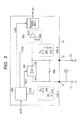
- FIG. 3 is a circuit diagram showing a modification of the oscillator circuit 10.
- the load capacity of the oscillator circuit 10 changes according to the first and second modes. Since a resonant condition varies with the change in the load capacity thereof, its oscillation frequency also changes. Specifically, as shown in FIG. 4 , when the load capacity increases, the oscillation frequency is reduced. The reduction in the oscillation frequency means that the frequency of the clock signal CLK outputted from the comparator circuit 400 is lowered. That is, when the operating mode is switched from the first mode to the second mode, the frequency of the clock signal CLK outputted from the comparator circuit 400 is reduced.
- a frequency dividing circuit 600 may be provided in a stage subsequent to the comparator circuit 400 as shown in FIG. 3 to keep the clock frequency constant without depending on the operating mode.
- the frequency dividing circuit 600 performs a frequency division of the clock signal CLK outputted from the comparator circuit 400 and thereby adjusts a clock frequency. More specifically, the frequency dividing circuit 600 performs switching of a frequency dividing ratio in such a manner that the frequency of the clock signal CLK becomes identical between the first mode and the second mode.
- the above control circuit 500 performs switching of the frequency dividing ratio of the frequency dividing circuit 600.
- the control circuit 500 outputs a third control signal CON3 corresponding to the mode signal MODE to the frequency dividing circuit 600 and thereby performs switching of the frequency dividing ratio of the frequency dividing circuit 600.
- the control circuit 500 performs switching of the frequency dividing ratio of the frequency dividing ratio 600 in such a manner than the frequency of the clock signal CLK becomes identical between the first mode and the second mode.
- a clock signal CLK having a constant frequency is outputted from the oscillator circuit 10.
- the drive capability of the inverter circuit 100 is variably controlled by the first control signal CON1.
- Various configuration examples are considered as for such an inverter circuit 100.
- FIG. 5 shows one configuration example of the inverter circuit 100.
- the inverter circuit 100 is provided with an NMOS transistor 110 and a variable current source 120.
- the gate, drain and source of the NMOS transistor 110 are respectively coupled to an input terminal 101 (first terminal T1), an output terminal 102 (second terminal T2) and a ground terminal.
- the variable current source 120 supplies current to the drain of the NMOS transistor 110, i.e., the output terminal 102 (second terminal T2).
- the current supplied from the variable current source 120 is controlled by the first control signal CON1 outputted from the control circuit 500. Specifically, the current of the variable current source 120 is controlled so as to be larger in the second mode than in the first mode. Thus, the drive capability of the inverter circuit 100 becomes larger in the second mode than in the first mode.
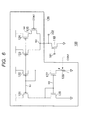
- FIG. 6 shows a configuration example of the variable current source 120.
- the variable current source 120 is provided with PMOS transistors 121 through 125, NMOS transistors 126 and 127 and a variable resistor 128.
- the gates of the PMOS transistors 121 through 124 are coupled in common to a node N1.
- the sources of the PMOS transistors 121 through 124 are coupled to a power supply terminal.
- the drain of the PMOS transistor 121 is coupled to a node N2.
- the drain of the PMOS transistor 122 is coupled to the node N1.
- the drain of the PMOS transistor 123 is coupled to a node N3.
- the drain of the PMOS transistor 124 is coupled to a node N4.
- the drain of the PMOS transistor 125 is coupled to the node N3, and the source thereof is coupled to the node N4.
- the first control signal CON1 is inputted to the gate of the PMOS transistor 125. That is, the PMOS transistor 125 is ON/OFF-controlled by the first control signal CON1.
- the gate and drain of the NMOS transistor 126 are both coupled to the node N2.
- the source of the NMOS transistor 126 is coupled to a ground terminal.
- the gate of the NMOS transistor 127 is coupled to the node N2, and the drain thereof is coupled to the node N1.
- the source of the NMOS transistor 127 is coupled to the ground terminal through the variable resistor 128.
- a resistance value of the variable resistor 128 is variably controlled by the first control signal CON1.
- the variable current source 120 is configured by such a current mirror circuit.
- a mirror ratio of the current mirror circuit can be switched by ON/OFF-controlling the PMOS transistor 125 using the first control signal CON1.
- a reference current of the current mirror circuit can be switched by controlling the resistance value of the variable resistor 128 using the first control signal CON1.
- the supply current of the variable current source 120 can be switched by such switching of the mirror ratio and/or reference current.
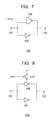
- FIG. 7 shows another configuration example of the inverter circuit 100.
- the inverter circuit 100 is provided with an inverter 130 and a NAND gate 140.
- An input terminal and an output terminal of the inverter 130 are respectively coupled to an input terminal 101 (first terminal T1) and an output terminal 102 (second terminal T2).
- One of input terminals of the NAND gate 140 is coupled to the input terminal 101 (first terminal T1), and the other thereof is inputted with the first control signal CON1.
- An output terminal of the NAND gate 140 is coupled to the output terminal 102 (second terminal T2).
- the output of the NAND gate 140 is fixed.
- the NAND gate 140 functions as an inverter. In this case, the drive capability of the entire inverter circuit 100 increases. That is, the drive capability of the entire inverter circuit 100 can be switched in response to the first control signal CON1.
- FIG. 8 shows a further configuration example of the inverter circuit 100.
- the inverter circuit 100 is provided with inverters 150 and 160 and a switch 170. Respective input terminals of the inverters 150 and 160 are coupled to an input terminal 101 (first terminal T1). On the other hand, respective output terminals of the inverters 150 and 160 are coupled to an output terminal 102 (second terminal T2). Further, the switch 170 is interposed between the inverter 160 and a power supply terminal.
- the switch 170 is ON/OFF-controlled by the first control signal CON1.
- the switch 170 When the switch 170 is ON, the inverter 160 operates, whereas when the switch 170 is OFF, the inverter 160 does not operate.
- the drive capability of the entire inverter circuit 100 can be switched in response to the first control signal CON1.
- variable capacitor 1 1 - 5.
- variable capacitor 1 1 - 5.
- variable capacitor 200-1 has been coupled to the first terminal T1
- second variable capacitor 200-2 has been coupled to the second terminal T2.
- the layout of each variable capacitor 200 is however not limited to it.
- the variable capacitor 200 may be coupled to at least one of the first terminal T1 and the second terminal T2, whereby the effect of improving noise immunity is obtained.
- the first variable capacitor 200-1 is provided and the second variable capacitor 200-2 may be omitted.
- the area of the oscillator circuit 10 is reduced.
- one variable capacitor 200 may be provided to couple between a first terminal T1 and a second terminal T2. Such a coupling configuration is preferred in that a "mirror effect" that the apparent capacity increases is expected. Since the number of the variable capacitors 200 is reduced, an area reducing effect is also obtained.
- the capacitance value of the variable capacitor 200 can be controlled by a second control signal CON2.
- the variable capacitor 200 is provided with a capacitor 230 and a switch 240 coupled in series between the first terminal T1 and the second terminal T2.
- a capacitance value coupled to each of the first terminal T1 and the second terminal T2 can be switched by ON/OFF-controlling the switch 240 by the second control signal CON2.
- a capacitor 210 in each variable capacitor 200 may be provided outside a semiconductor chip as with a first capacitor C1 and a second capacitor C2. It is thus possible to suppress an increase in chip area.
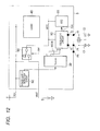
- FIG. 12 shows a configuration example of a semiconductor device (semiconductor chip 5) to which the oscillator circuit 10 according to the present embodiment is applied.
- the semiconductor chip 5 is coupled to a power supply 2 and supplied with a power supply voltage VCC (normal power supply voltage) from the power supply 2.
- the semiconductor chip 5 is coupled to a battery 3 used as a backup power supply and supplied with a battery power supply voltage VBAT (backup power supply voltage) from the battery 3.
- VCC normal power supply voltage
- VBAT backup power supply voltage
- the semiconductor chip 5 is provided with the above oscillator circuit 10, an RTC (Real Time Clock) circuit 20, a system controller 30, a logic circuit 40, a power supply switching circuit 50 and a power supply detection circuit 60.
- RTC Real Time Clock
- the first and second terminals T1 and T2 of the oscillator circuit 10 are respectively coupled to first and second pins P1 and P2 of the semiconductor chip 5.
- the first pin P1 and the second pin P2 are coupled to a crystal resonator 1 and the like that are external parts. Specifically, the first pin P1 and the second pin P2 are coupled to both ends of the crystal resonator 1.
- the first pin P1 is coupled to a first capacitor C1
- the second pin P2 is coupled to a second capacitor C2.
- the oscillator circuit 10 generates and outputs a clock signal CLK.
- the RTC circuit 20 receives the clock signal CLK generated by the oscillator circuit 10 therein and operates based on the clock signal CLK.
- the system controller 30 controls the entire operation of the semiconductor chip 5. For example, the system controller 30 generates the above mode signal MODE in response to the operating mode of the semiconductor chip 5 and outputs the mode signal MODE to the oscillator circuit 10. Thus, the oscillator circuit 10 performs an operation corresponding to the mode signal MODE.
- the logic circuit 40 operates based on the power supply voltage VCC and provides a prescribed function.
- the oscillator circuit 10 and the RTC circuit 20 are used in a timer, they are required to always operate.
- the power supply voltage VCC is lowered, for example, the battery power supply voltage VBAT is supplied to the oscillator circuit 10 and the RTC circuit 20 instead of the power supply voltage VCC. That is, the power supply voltage (hereinafter referred to as "RTC power supply voltage VRTC") supplied to the oscillator circuit 10 and the RTC circuit 20 can be switched between the power supply voltage VCC and the battery power supply voltage VBAT according to the circumstances.
- the power supply switching circuit 50 and the power supply detection circuit 60 are provided to perform automatic switching of such an RTC power supply voltage VRTC.
- the power supply switching circuit 50 receives the power supply voltage VCC and the battery power supply voltage VBAT and supplies either of them to the oscillator circuit 10 and the RTC circuit 20 as the RTC power supply voltage VRTC.
- the RTC power supply voltage VRTC is specified by a power supply switch signal SW. That is, the power supply switching circuit 50 switches the RTC power supply voltage VRTC between the power supply voltage VCC and the battery power supply voltage VBAT in response to the power supply switch signal SW.
- the power supply detection circuit 60 monitors the power supply voltage VCC. When the power supply voltage VCC reaches a prescribed threshold value or less, the power supply detection circuit 60 outputs a power supply reduction signal to the system controller 30. In response to the power supply reduction signal, the system controller 30 outputs the power supply switch signal SW to the power supply switching circuit 50 and thereby controls power supply switching. Specifically, the system controller 30 controls the power supply switching circuit 50 in such a manner that the RTC power supply voltage VRTC is switched from the power supply voltage VCC to the battery power supply voltage VBAT.
- the power supply detection circuit 60 outputs a power supply recovery signal to the system controller 30.
- the system controller 30 outputs the power supply switch signal SW to the power supply switching circuit 50 and thereby controls power supply switching.
- the system controller 30 controls the power supply switching circuit 50 in such a manner that the RTC power supply voltage VRTC is switched from the battery power supply voltage VBAT to the power supply voltage VCC.
- the oscillator circuit 10 is a circuit that performs weak oscillations with small current. There is therefore a possibility that a signal inputted to a pin PA (refer to FIG. 12 ) adjacent to the first pin P1 coupled to the oscillator circuit 10 and the crystal resonator 1 will exert an influence on the operation of the oscillator circuit 10. It is thus desirable that the adjacent pin PA is such a pin as not to be used in a final product. For example, it is desirable that the adjacent pin PA is a pin used in a "debug mode" that performs emulation of the semiconductor chip 5.
- FIG. 13 shows a state in the debug mode.
- the adjacent pin PA is coupled to an external emulator (not shown).
- a debug is performed through the adjacent pin PA by using the emulator.
- coupling occurs between a wiring coupled to the adjacent pin PA and the oscillator circuit 10. Accordingly, the malfunction (clock reduction or losing or the like) of the oscillator circuit 10 might occur due to noise of the adjacent pin PA in the debug mode.
- the oscillator circuit 10 is effective against such noise of the adjacent pin PA in the debug mode. That is, the second mode that is of the high noise-immunity mode may preferably be associated with the debug mode that performs emulation.
- the first mode that is of the low power mode is a mode in which no emulation is conducted.
- a mode signal MODE indicative of whether it is the debug mode is hereinafter referred to as a "debug mode signal XMOD".
- the debug mode signal XMOD is supplied from the system controller 30 to the oscillator circuit 10. That is, the switching of the operating mode is automatically controlled by the system controller 30.
- FIG. 14 is a timing chart showing a method for controlling the oscillator circuit 10 according to the present embodiment.
- a debug mode signal XMOD of a Low level is assumed to indicate a first mode
- a debug mode signal XMOD of a High level is assumed to indicate a second mode (debug mode).
- the debug mode signal XMOD is changed from the Low level to the High level.
- the operating mode is switched from the first mode to the second mode (debug mode).
- the control circuit 500 performs control to increase "both" of the drive capability of the inverter circuit 100 and the capacitance value of each variable capacitor 200. Specifically, the control circuit 500 increases the drive capability of the inverter circuit 100 at a time t1 subsequent to the time t0 and further increases the capacitance value of the variable capacitor 200 at a time t2 after the time t1.
- the influence of coupling to the adjacent pin PA becomes small.
- the value of the capacitance coupled to the first terminal T1 increases from 3pF to 12pF
- the influence of coupling to the adjacent pin PA is reduced approximately to 1/4.
- the malfunction of the oscillator circuit 10 due to the noise of the adjacent pin PA is effectively suppressed.
- emulation using the adjacent pin PA is permitted.
- the debug mode signal XMOD is changed from the High level to the Low level at a time t3.
- the operating mode is switched from the second mode (debug mode) to the first mode.
- the control circuit 500 performs control to decrease "both" of the drive capability of the inverter circuit 100 and the capacitance value of each variable capacitor 200. Specifically, the control circuit 500 decreases the capacitance value of the variable capacitor 200 at a time t4 subsequent to the time t3 and further decreases the drive capability of the inverter circuit 100 at a time t5 subsequent to the time t4. Thus, power consumption is reduced.
- the adjacent pin PA used in the emulation adjoins the first pin P1
- only the first variable capacitor 200-1 on the first pin P1 side close to a noise source may be provided (refer to FIG. 9 ). Even in this case, significant high noise immunity is obtained.
- the effect of reducing an area is obtained by omitting the second variable capacitor 200-2 on the second pin P2 side.
- the switching of the RTC power supply voltage VRTC is automatically performed by the power supply switching circuit 50, the power supply detection circuit 60 and the system controller 30 (refer to FIG. 12 ).
- the switching of the RTC power supply voltage VRTC will be described in more detail referring to FIG. 15 .
- the RTC power supply voltage VRTC is of a power supply voltage VCC.
- the power supply voltage VCC begins to drop.
- the power supply voltage VCC falls below a predetermined threshold value Vt.
- the system controller 30 outputs a power supply switch signal SW to the power supply switching circuit 50 and thereby changes the RTC power supply voltage VRTC from the power supply voltage VCC to a battery power supply voltage VBAT. Since, however, a response delay actually occurs, the RTC power supply voltage VRTC is changed from the power supply voltage VCC to the battery power supply voltage VBAT at a time t12 subsequent to the time t11.
- the RTC power supply voltage VRTC is of the battery power supply voltage VBAT. Thereafter, the power supply voltage VCC begins to rise. At a time t21, the power supply voltage VCC exceeds the predetermined threshold value Vt. In response to it, the system controller 30 outputs the power supply switch signal SW to the power supply switching circuit 50 and thereby changes the RTC power supply voltage VRTC from the battery power supply voltage VBAT to the power supply voltage VCC. Since, however, a response delay actually occurs, the RTC power supply voltage VRTC is changed from the battery power supply voltage VBAT to the power supply voltage VCC at a time t22 subsequent to the time t21.
- the RTC power supply voltage VRTC is reduced from the level of the power supply voltage VCC for a while upon power supply switching. Particularly during the period from the times t10 to t12 in which the power supply voltage VCC is reduced, the RTC power supply voltage VRTC is also greatly reduced. These lead to the malfunction (clock reduction or the like) of the oscillator circuit 10.
- the oscillator circuit 10 is effective against the voltage reduction at such switching of the RTC power supply voltage VRTC. That is, the second mode that is of the high noise-immunity mode may preferably be associated with a mode that "permits" the switching of the RTC power supply voltage VRTC. On the other hand, the first mode that is of the low power mode is associated with a mode that "prohibits" the switching of the RTC power supply voltage VRTC.
- the mode signal MODE indicative of the permission/prohibition of switching is hereinafter referred to as a "power-supply switch permission signal XVOL".
- the power-supply switch permission signal XVOL is supplied from the system controller 30 to the oscillator circuit 10. That is, the switching of the operating mode is automatically controlled by the system controller 30.
- FIG. 16 is a timing chart showing the control method of the oscillator circuit 10 according to the present embodiment.
- a power-supply switch permission signal XVOL of a Low level is assumed to show the first mode (switching prohibition).
- a power-supply switch permission signal XVOL of a High level is assumed to show the second mode (switching permission).
- the control circuit 500 performs control to decrease "both" of the drive capability of the inverter circuit 100 and the capacitance value of each variable capacitor 200. Specifically, the control circuit 500 decreases the capacitance value of the variable capacitor 200 at a time t34 subsequent to the time t33. Further, the control circuit 500 decreases the drive capability of the inverter circuit 100 at a time t35 subsequent to the time t34. Thus, power consumption is reduced.
- the period from the times t32 to t34 is a power-supply switch permission period during which the switching of the RTC power supply voltage VRTC is permitted.
- the system controller 30 performs switching of the power supply switch signal SW in such a manner that the RTC power supply voltage VRTC is switched during the power-supply switch permission period.
- the system controller 30 switches the power-supply switch permission signal XVOL from the Low level to the High level prior to the switching of the power supply switch signal SW.
- the system controller 30 switches the power-supply switch permission signal XVOL from the High level to the Low level.
- the control circuit 500 performs control to decrease "both" of the drive capability of the inverter circuit 100 and the capacitance value of each variable capacitor 200. Specifically, the control circuit 500 decreases the capacitance value of the variable capacitor 200 at a time t44 subsequent to the time t43. Further, the control circuit 500 decreases the drive capability of the inverter circuit 100 at a time t45 subsequent to the time t44. Thus, power consumption is reduced.
- the period from the times t42 to t44 is a power-supply switch permission period during which the switching of the RTC power supply voltage VRTC is permitted.
- the system controller 30 performs switching of the power supply switch signal SW in such a manner that the RTC power supply voltage VRTC is switched during the power-supply switch permission period.
- the system controller 30 switches the power-supply switch permission signal XVOL from the Low level to the High level prior to the switching of the power supply switch signal SW.
- the system controller 30 switches the power-supply switch permission signal XVOL from the High level to the Low level.
- the drive current and load capacity of the oscillator circuit 10 increases during the power-supply switch permission period in this manner.
- the switching of the RTC power supply voltage VRTC during the power-supply switch permission period enables an influence exerted on the operation of the oscillator circuit 10 by its switching to be minimized.
- the operating mode of the oscillator circuit 10 may preferably be set to the second mode at the start and stop of the operation of the function block. It is thus possible to minimize an influence exerted on the operation of the oscillator circuit 10 due to the noise from the function block.
- the comparator circuit 400 is provided with a differential comparator 410.
- Two inputs of the comparator 410 are coupled to their corresponding first and terminals T1 and T2.
- the comparator 410 performs a differential operation, an output is obtained if a difference in potential occurs even slightly between the first and second terminals T1 and T2.
- inphase noise are applied to the first and second terminals T1 and T2, they are cancelled and do not affect a clock signal CLK.
- the comparator circuit 400 of the present example is particularly effective in switching of the power supply voltage (refer to the section 2 - 3).
- FIG. 18 shows a capacitively-coupled comparator circuit 400. More specifically, the comparator circuit 400 is provided with a comparator 430, a capacitor 440, a resistor 450, a reference voltage power supply 460 and a capacitor 470. Two inputs of the comparator 430 are respectively coupled to a node 401 and a node 402. The capacitor 440 is coupled between the node 401 and an output terminal 102 of an inverter circuit 100. The resistor 450 is coupled between the node 401 and the node 402. The reference voltage power supply 460 is coupled to the node 402 and supplies a reference voltage to the node 402. The capacitor 470 is coupled between the node 402 and a ground terminal. Even when a DC operating point (center voltage of oscillation) shifts for some reason, an output is obtained by capacitive coupling of the input of the comparator 430 without problems.
- a DC operating point center voltage of oscillation
- FIG. 19 shows a hybrid comparator circuit 400. More specifically, both of the comparator circuit 400 shown in FIG. 1 and the comparator circuit 400 shown in FIG. 18 are provided.
- the comparator circuit 400 shown in FIG. 1 generates a first clock signal CLK1.
- the comparator circuit 400 shown in FIG. 18 generates a second clock signal CLK2.
- a selection circuit 480 receives the first clock signal CLK1 and the second clock signal CLK2 and outputs one of them as a clock signal CLK. It is preferred in that the proper one of the first and second clock signals CLK1 and CLK2 can selectively be used according to the operating mode.
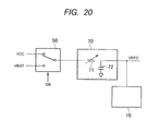
- FIG. 20 shows another configuration example for improving noise immunity relative to power supply switching.
- a low-pass filter 70 is provided on a power supply line for supplying an RTC power supply voltage VRTC to an oscillator circuit 10.
- the low-pass filter 70 is provided with a variable resistor 71 and a capacitor 72.
- the resistance value of the variable resistor 71 in the low-pass filter 70 is changed in response to a power-supply switch permission signal XVOL. Specifically, the resistance value of the variable resistor 71 in the low-pass filter 70 increases during the above power-supply switch permission period. Thus, the slope of a fluctuation in the RTC power supply voltage VRTC becomes gentle, so that the occurrence of a malfunction of the oscillator circuit 10 is suppressed.
Landscapes
- Oscillators With Electromechanical Resonators (AREA)
- Semiconductor Integrated Circuits (AREA)
- Engineering & Computer Science (AREA)
- Power Engineering (AREA)
- Theoretical Computer Science (AREA)
Abstract
Description
- The disclosure of Japanese Patent Application No.
2012-170337 filed on July 31, 2012 - The present invention relates to a semiconductor device equipped with an oscillator circuit, and a control method thereof.
- A clock signal used in a semiconductor device is generated typically by using a crystal resonator and an oscillator circuit. It is desirable that noise immunity of the oscillator circuit is high to obtain a stable clock signal.
- A
Patent Document 1 has disclosed an oscillator circuit. The oscillator circuit has an inverter having a transistor, a feedback resistor, capacitive elements, a variable current source, a timer circuit, and a current controller. The feedback resistor is coupled in parallel with the inverter. The capacitive elements are respectively provided on the input and output sides of the inverter. The variable current source supplies either of two types of currents different in level to the inverter. The timer circuit counts a prescribed time from the start-up of a power supply for the oscillator circuit. The current controller controls the variable current source in such a manner that it supplies the current large in level, of the two types of currents suppliable by the variable current source to the inverter during a period taken until the count time by the timer circuit goes beyond a predetermined time and that after it has gone beyond the predetermined time, it supplies the current small in level to the inverter. - A
Patent Document 2 has disclosed a crystal oscillator circuit in which a power supply line is made identical with other electronic circuits. A low-pass filter for preventing noise superimposed on the power supply line from entering the crystal oscillator circuit is provided between the power supply line and the crystal oscillator circuit. - A
Patent Document 3 has disclosed a crystal oscillator. The crystal oscillator is equipped with a crystal oscillator circuit and a buffer circuit. The crystal oscillator circuit is coupled to a power supply circuit and takes the output of a control voltage generating circuit as an input. The buffer circuit is coupled to the power supply circuit and takes the output of the crystal oscillator circuit as an input. Further, a low-pass filter is coupled between the power supply circuit and the buffer circuit. -
- [Patent Document 1] Japanese Unexamined Patent Publication Laid-Open No.
2009-105611 - [Patent Document 2] Japanese Unexamined Patent Publication Laid-Open No.
2001-136030 - [Patent Document 3] Japanese Unexamined Patent Publication Laid-Open No.
2008-103808 - Driving small capacity capacitors with low current is effective to suppress power consumption of an oscillator circuit. Such small capacity capacitors are however low in immunity against noise and environmental variations such as fluctuations in power supply voltage, etc. Thus, when the oscillator circuit is implemented in a product chip, such small capacity capacitors have a potential for becoming a cause of a malfunction of the oscillator circuit. Compatibility of low power consumption and high noise immunity has been desired for the oscillator circuit.
- Other objects and novel features of the present invention will become apparent from the description of the present specification and the accompanying drawings.
- In one embodiment, a semiconductor device is provided. The semiconductor device is provided with a first terminal and a second terminal respectively coupled to both ends of a crystal resonator. The semiconductor device is further provided with an inverter circuit, a feedback resistor, a variable capacitor and a control circuit. The input of the inverter circuit is coupled to the first terminal, and its output is coupled to the second terminal. The feedback resistor couples between the first terminal and the second terminal. The variable capacitor is coupled to at least one of the first terminal and the second terminal. The control circuit controls the drive capability of the inverter circuit and the capacitance value of the variable capacitor, based on a mode signal which specifies each of a first mode and a second mode. More specifically, the control circuit performs control to increase both of the drive capability of the inverter circuit and the capacitance value of the variable capacitor in the second mode rather than the first mode.
- In one embodiment, a control method of a semiconductor device is provided. The semiconductor device is provided with a first terminal and a second terminal respectively coupled to both ends of a crystal resonator, an inverter circuit having an input coupled to the first terminal and an output coupled to the second terminal, a feedback resistor which couples between the first terminal and the second terminal, and a variable capacitor coupled to at least one of the first and second terminals. The control method includes (A) a step of switching an operating mode between a first mode and a second mode, and (B) a step of performing control in such a manner that both of the drive capability of the inverter circuit and the capacitance value of the variable capacitor become larger in the second mode than in the first mode.
- Compatibility of low power consumption and high noise immunity can be realized with respect to an oscillator circuit.
-
-
FIG. 1 is a circuit diagram showing a configuration of an oscillator circuit according to an embodiment of the present invention; -
FIG. 2 is a timing chart illustrating a control method of the oscillator circuit according to the embodiment of the present invention; -
FIG. 3 is a circuit diagram depicting a modification of the oscillator circuit according to the embodiment of the present invention; -
FIG. 4 is a conceptual diagram for describing the operation of a frequency dividing circuit; -
FIG. 5 is a circuit diagram showing a configuration example of an inverter circuit in the oscillator circuit according to the embodiment of the present invention; -
FIG. 6 is a circuit diagram illustrating the configuration example of the inverter circuit in the oscillator circuit according to the embodiment of the present invention; -
FIG. 7 is a circuit diagram showing another configuration example of the inverter circuit in the oscillator circuit according to the embodiment of the present invention; -
FIG. 8 is a circuit diagram illustrating a further configuration example of the inverter circuit in the oscillator circuit according to the embodiment of the present invention; -
FIG. 9 is a circuit diagram depicting a modification of the oscillator circuit according to the embodiment of the present invention; -
FIG. 10 is a circuit diagram showing another modification of the oscillator circuit according to the embodiment of the present invention; -
FIG. 11 is a circuit diagram illustrating a further modification of the oscillator circuit according to the embodiment of the present invention; -
FIG. 12 a block diagram showing a configuration example of a semiconductor device according to an embodiment of the present invention; -
FIG. 13 is a circuit diagram for describing an application example of the oscillator circuit according to the embodiment of the present invention; -
FIG. 14 is a timing chart for describing the application example of the oscillator circuit according to the embodiment of the present invention; -
FIG. 15 is a conceptual diagram for describing another application example of the oscillator circuit according to the embodiment of the present invention; -
FIG. 16 is a timing chart for describing another application example of the oscillator circuit according to the embodiment of the present invention; -
FIG. 17 is a circuit diagram showing a modification of a comparator circuit in the oscillator circuit according to the embodiment of the present invention; -
FIG. 18 is a circuit diagram illustrating another modification of the comparator circuit in the oscillator circuit according to the embodiment of the present invention; -
FIG. 19 is a circuit diagram depicting a further modification of the comparator circuit in the oscillator circuit according to the embodiment of the present invention; and -
FIG. 20 is a block diagram showing a modification of the semiconductor device according to the embodiment of the present invention. -
FIG. 1 is a circuit diagram showing a configuration of anoscillator circuit 10 according to an embodiment of the present invention. Theoscillator circuit 10 is coupled to acrystal resonator 1, a first capacitor C1 and a second capacitor C2 that are external parts. More specifically, theoscillator circuit 10 has a first terminal T1 and a second terminal T2. The first terminal T1 and the second terminal T2 are respectively coupled to both ends of thecrystal resonator 1. The first capacitor C1 is coupled between the first terminal T1 and a ground terminal. The second capacitor C2 is coupled between the second terminal T2 and the ground terminal. Theoscillator circuit 10 operates in conjunction with thesecrystal resonator 1, first capacitor C1 and second capacitor C2 and thereby generates and outputs a clock signal CLK. - The
oscillator circuit 10 is provided with aninverter circuit 100, afeedback resistor 300 and acomparator circuit 400. - The
inverter circuit 100 has an inverting logic function and performs logic inversion between aninput terminal 101 and anoutput terminal 102. Theinput terminal 101 and theoutput terminal 102 of theinverter circuit 100 are respectively coupled to the first terminal T1 and the second terminal T2. Incidentally, as will be described later, the drive capability of theinverter circuit 100 according to the present embodiment can be variably controlled. - The
feedback resistor 300 is provided to couple between the first terminal T1 and the second terminal T2. Thecrystal resonator 1, first capacitor C1, second capacitor C2,inverter circuit 100 andfeedback resistor 300 described above generates oscillating operations as with a typical oscillator circuit. - An input of the
comparator circuit 400 is coupled to the second terminal T2 (theoutput terminal 102 of the inverter circuit 100). Thecomparator circuit 400 generates a clock signal CLK, based on a voltage (oscillation voltage waveform) of the second terminal T2 and outputs the generated clock signal CLK. For example, thecomparator circuit 400 is provided with acomparator 410 and a referencevoltage power supply 420. The referencevoltage power supply 420 generates a reference voltage. The reference voltage and the voltage of the second terminal T2 are inputted to thecomparator 410, so that the clock signal CLK is generated. - The
oscillator circuit 10 according to the present embodiment is further provided withvariable capacitors 200 and acontrol circuit 500. - The
variable capacitor 200 is coupled to at least one of the first terminal T1 and the second terminal T2. In the example shown inFIG. 1 , a first variable capacitor 200-1 is coupled to the first terminal T1, and a second variable capacitor 200-2 is coupled to the second terminal T2. A capacitance value coupled to the first terminal T1 (second terminal T2) can be variably controlled by controlling the capacitance value of the first variable capacitor 200-1 (second variable capacitor 200-2). For example, eachvariable capacitor 200 is provided with acapacitor 210 and aswitch 220. The capacitance value of thecapacitor 210 is 10pF, for example. Theswitch 220 is interposed between thecapacitor 210 and the first terminal T1 (second terminal T2). The capacitance value coupled to the first terminal T1 (second terminal T2) can be variably controlled by ON/OFF-controlling theswitch 220. - In the present embodiment, the drive capability of the
inverter circuit 100 and the capacitance vale of eachvariable capacitor 200 can be variably controlled. Thecontrol circuit 500 performs its variable control. Specifically, thecontrol circuit 500 outputs a first control signal CON1 to theinverter circuit 100 and thereby controls the drive capability of theinverter circuit 100. Also thecontrol circuit 500 outputs a second control signal CON2 to the respectivevariable capacitors 200 and thereby controls the capacitance values of thevariable capacitors 200. - The control by the
control circuit 500 is performed based on a mode signal MODE. The mode signal MODE specifies either of a "first mode" and a "second mode". Thecontrol circuit 500 outputs the first control signal CON1 and the second control signal CON2 in response to the content (first mode or second mode) of the mode signal MODE. That is, thecontrol circuit 500 controls the drive capability of theinverter circuit 100 and the capacitance value of eachvariable capacitor 200 in response to the mode signal MODE. -
FIG. 2 is a timing chart showing a control method of theoscillator circuit 10 according to the present embodiment. In the present embodiment, a mode signal MODE of a Low level indicates a first mode, and a mode signal MODE of a High level indicates a second mode. - At a time t0, the mode signal MODE is changed from the Low level to the High level. Thus, an operating mode is changed from the first mode to the second mode. In this case, the
control circuit 500 performs control to increase "both" of the drive capability of theinverter circuit 100 and the capacitance value of eachvariable capacitor 200. That is, both of the drive capability of theinverter circuit 100 and the capacitance value of thevariable capacitor 200 become larger in the second mode than in the first mode. As a result, since the drive current and load capacity of the oscillator circuit increase in the second mode, noise immunity of theoscillator circuit 10 is greatly improved. - Here, since the load capacity becomes larger than the drive current when the capacitance value of each
variable capacitor 200 increases before the increase in the drive capability of theinverter circuit 100, the amplitude of an oscillation voltage becomes small and oscillation stability is degraded. In the worst case, there is also a possibility that the oscillations will stop. In terms of the maintenance of oscillations, thecontrol circuit 500 preferably performs the following control upon switching from the first mode to the second mode. That is, thecontrol circuit 500 increases the drive capability of theinverter circuit 100 at a time t1 subsequent to the time t0 and further increases the capacitance value of thevariable capacitor 200 at a time t2 subsequent to the time t1. Thus, since the load capacity increases after the drive current has increased, degradation in the oscillation stability is prevented without the amplitude of the oscillation voltage being extremely reduced. - At a time t3, the mode signal MODE is switched from the High level to the Low level. Thus, the operating mode is switched from the second mode to the first mode. In this case, the
control circuit 500 performs control to decrease "both" of the drive capability of theinverter circuit 100 and the capacitance value of eachvariable capacitor 200. Even here, in terms of the maintenance of oscillations, thecontrol circuit 500 preferably performs the following control. That is, thecontrol circuit 500 decreases the capacitance value of thevariable capacitor 200 at a time t4 subsequent to the time t3 and further reduces the drive capability of theinverter circuit 100 at a time t5 subsequent to the time t4. Thus, since the load capacity is reduced before the drive current is reduced, degradation in the oscillation stability is prevented from occurring. - According to the present embodiment as described above, both of the drive current and load capacity of the
oscillator circuit 10 become larger in the second mode than in the first mode. As a result, in the second mode, noise immunity of theoscillator circuit 10 is greatly improved. On the other hand, since both of the load capacity and the drive current are small, power consumption is suppressed. That is, it can also be said that the first mode is a "low power mode" and the second mode is a "high noise-immunity mode". - Driving small capacity capacitors (C1 and C2) with low current is effective to suppress the power consumption of the
oscillator circuit 10. The suppression of the power consumption is realized by the first mode. For example, when only a timer (RTC circuit) built in a semiconductor device is operated at standby, it is considered that the operating mode is set to the first mode. It is thus possible to lengthen a battery drive time at standby. - On the other hand, such small capacity capacitors (C1 and C2) are low in immunity against noise and environmental variations such as fluctuations in power supply voltage, etc. When the
oscillator circuit 10 is implemented in a product chip, such small capacity capacitors (C1 and C2) have a potential for becoming a cause of a malfunction in theoscillator circuit 10. Thus, when high noise immunity is desired, the second mode is preferably used. Since the drive current and the load capacity increase, the noise immunity of theoscillator circuit 10 is greatly improved. - Properly using the first and second modes depending on the circumstances in this manner enables compatibility between low power consumption and high noise immunity.
-
FIG. 3 is a circuit diagram showing a modification of theoscillator circuit 10. As described above, in the present embodiment, the load capacity of theoscillator circuit 10 changes according to the first and second modes. Since a resonant condition varies with the change in the load capacity thereof, its oscillation frequency also changes. Specifically, as shown inFIG. 4 , when the load capacity increases, the oscillation frequency is reduced. The reduction in the oscillation frequency means that the frequency of the clock signal CLK outputted from thecomparator circuit 400 is lowered. That is, when the operating mode is switched from the first mode to the second mode, the frequency of the clock signal CLK outputted from thecomparator circuit 400 is reduced. - Thus, a frequency dividing circuit 600 may be provided in a stage subsequent to the
comparator circuit 400 as shown inFIG. 3 to keep the clock frequency constant without depending on the operating mode. The frequency dividing circuit 600 performs a frequency division of the clock signal CLK outputted from thecomparator circuit 400 and thereby adjusts a clock frequency. More specifically, the frequency dividing circuit 600 performs switching of a frequency dividing ratio in such a manner that the frequency of the clock signal CLK becomes identical between the first mode and the second mode. - The
above control circuit 500 performs switching of the frequency dividing ratio of the frequency dividing circuit 600. Thecontrol circuit 500 outputs a third control signal CON3 corresponding to the mode signal MODE to the frequency dividing circuit 600 and thereby performs switching of the frequency dividing ratio of the frequency dividing circuit 600. Specifically, thecontrol circuit 500 performs switching of the frequency dividing ratio of the frequency dividing ratio 600 in such a manner than the frequency of the clock signal CLK becomes identical between the first mode and the second mode. Thus, a clock signal CLK having a constant frequency is outputted from theoscillator circuit 10. - As mentioned above, the drive capability of the
inverter circuit 100 is variably controlled by the first control signal CON1. Various configuration examples are considered as for such aninverter circuit 100. -
FIG. 5 shows one configuration example of theinverter circuit 100. In the example shown inFIG. 5 , theinverter circuit 100 is provided with anNMOS transistor 110 and a variablecurrent source 120. The gate, drain and source of theNMOS transistor 110 are respectively coupled to an input terminal 101 (first terminal T1), an output terminal 102 (second terminal T2) and a ground terminal. The variablecurrent source 120 supplies current to the drain of theNMOS transistor 110, i.e., the output terminal 102 (second terminal T2). - The current supplied from the variable
current source 120 is controlled by the first control signal CON1 outputted from thecontrol circuit 500. Specifically, the current of the variablecurrent source 120 is controlled so as to be larger in the second mode than in the first mode. Thus, the drive capability of theinverter circuit 100 becomes larger in the second mode than in the first mode. -
FIG. 6 shows a configuration example of the variablecurrent source 120. The variablecurrent source 120 is provided withPMOS transistors 121 through 125,NMOS transistors variable resistor 128. - The gates of the
PMOS transistors 121 through 124 are coupled in common to a node N1. The sources of thePMOS transistors 121 through 124 are coupled to a power supply terminal. The drain of thePMOS transistor 121 is coupled to a node N2. The drain of thePMOS transistor 122 is coupled to the node N1. The drain of thePMOS transistor 123 is coupled to a node N3. The drain of thePMOS transistor 124 is coupled to a node N4. - The drain of the
PMOS transistor 125 is coupled to the node N3, and the source thereof is coupled to the node N4. The first control signal CON1 is inputted to the gate of thePMOS transistor 125. That is, thePMOS transistor 125 is ON/OFF-controlled by the first control signal CON1. - The gate and drain of the
NMOS transistor 126 are both coupled to the node N2. The source of theNMOS transistor 126 is coupled to a ground terminal. The gate of theNMOS transistor 127 is coupled to the node N2, and the drain thereof is coupled to the node N1. The source of theNMOS transistor 127 is coupled to the ground terminal through thevariable resistor 128. A resistance value of thevariable resistor 128 is variably controlled by the first control signal CON1. - The variable
current source 120 is configured by such a current mirror circuit. A mirror ratio of the current mirror circuit can be switched by ON/OFF-controlling thePMOS transistor 125 using the first control signal CON1. Alternatively, a reference current of the current mirror circuit can be switched by controlling the resistance value of thevariable resistor 128 using the first control signal CON1. The supply current of the variablecurrent source 120 can be switched by such switching of the mirror ratio and/or reference current. -
FIG. 7 shows another configuration example of theinverter circuit 100. In the example shown inFIG. 7 , theinverter circuit 100 is provided with aninverter 130 and aNAND gate 140. An input terminal and an output terminal of theinverter 130 are respectively coupled to an input terminal 101 (first terminal T1) and an output terminal 102 (second terminal T2). One of input terminals of theNAND gate 140 is coupled to the input terminal 101 (first terminal T1), and the other thereof is inputted with the first control signal CON1. An output terminal of theNAND gate 140 is coupled to the output terminal 102 (second terminal T2). - When the first control signal CON1 is a Low level, the output of the
NAND gate 140 is fixed. On the other hand, when the first control signal CON1 is a High level, theNAND gate 140 functions as an inverter. In this case, the drive capability of theentire inverter circuit 100 increases. That is, the drive capability of theentire inverter circuit 100 can be switched in response to the first control signal CON1. -
FIG. 8 shows a further configuration example of theinverter circuit 100. In the example shown inFIG. 8 , theinverter circuit 100 is provided withinverters switch 170. Respective input terminals of theinverters inverters switch 170 is interposed between theinverter 160 and a power supply terminal. - The
switch 170 is ON/OFF-controlled by the first control signal CON1. When theswitch 170 is ON, theinverter 160 operates, whereas when theswitch 170 is OFF, theinverter 160 does not operate. Thus, the drive capability of theentire inverter circuit 100 can be switched in response to the first control signal CON1. - In the already-mentioned example of
FIG. 1 , the first variable capacitor 200-1 has been coupled to the first terminal T1, and the second variable capacitor 200-2 has been coupled to the second terminal T2. The layout of eachvariable capacitor 200 is however not limited to it. Thevariable capacitor 200 may be coupled to at least one of the first terminal T1 and the second terminal T2, whereby the effect of improving noise immunity is obtained. - As shown in
FIG. 9 , for example, only the first variable capacitor 200-1 is provided and the second variable capacitor 200-2 may be omitted. In this case, as compared with the case ofFIG. 1 , the area of theoscillator circuit 10 is reduced. - As shown in
FIG. 10 , onevariable capacitor 200 may be provided to couple between a first terminal T1 and a second terminal T2. Such a coupling configuration is preferred in that a "mirror effect" that the apparent capacity increases is expected. Since the number of thevariable capacitors 200 is reduced, an area reducing effect is also obtained. Incidentally, the capacitance value of thevariable capacitor 200 can be controlled by a second control signal CON2. For example, thevariable capacitor 200 is provided with a capacitor 230 and aswitch 240 coupled in series between the first terminal T1 and the second terminal T2. A capacitance value coupled to each of the first terminal T1 and the second terminal T2 can be switched by ON/OFF-controlling theswitch 240 by the second control signal CON2. - As shown in
FIG. 11 , acapacitor 210 in eachvariable capacitor 200 may be provided outside a semiconductor chip as with a first capacitor C1 and a second capacitor C2. It is thus possible to suppress an increase in chip area. -
FIG. 12 shows a configuration example of a semiconductor device (semiconductor chip 5) to which theoscillator circuit 10 according to the present embodiment is applied. Thesemiconductor chip 5 is coupled to apower supply 2 and supplied with a power supply voltage VCC (normal power supply voltage) from thepower supply 2. Thesemiconductor chip 5 is coupled to abattery 3 used as a backup power supply and supplied with a battery power supply voltage VBAT (backup power supply voltage) from thebattery 3. - The
semiconductor chip 5 is provided with theabove oscillator circuit 10, an RTC (Real Time Clock)circuit 20, asystem controller 30, alogic circuit 40, a powersupply switching circuit 50 and a powersupply detection circuit 60. - The first and second terminals T1 and T2 of the
oscillator circuit 10 are respectively coupled to first and second pins P1 and P2 of thesemiconductor chip 5. The first pin P1 and the second pin P2 are coupled to acrystal resonator 1 and the like that are external parts. Specifically, the first pin P1 and the second pin P2 are coupled to both ends of thecrystal resonator 1. The first pin P1 is coupled to a first capacitor C1, and the second pin P2 is coupled to a second capacitor C2. As mentioned above, theoscillator circuit 10 generates and outputs a clock signal CLK. - The
RTC circuit 20 receives the clock signal CLK generated by theoscillator circuit 10 therein and operates based on the clock signal CLK. - The
system controller 30 controls the entire operation of thesemiconductor chip 5. For example, thesystem controller 30 generates the above mode signal MODE in response to the operating mode of thesemiconductor chip 5 and outputs the mode signal MODE to theoscillator circuit 10. Thus, theoscillator circuit 10 performs an operation corresponding to the mode signal MODE. - The
logic circuit 40 operates based on the power supply voltage VCC and provides a prescribed function. - Since the
oscillator circuit 10 and theRTC circuit 20 are used in a timer, they are required to always operate. Thus, when the power supply voltage VCC is lowered, for example, the battery power supply voltage VBAT is supplied to theoscillator circuit 10 and theRTC circuit 20 instead of the power supply voltage VCC. That is, the power supply voltage (hereinafter referred to as "RTC power supply voltage VRTC") supplied to theoscillator circuit 10 and theRTC circuit 20 can be switched between the power supply voltage VCC and the battery power supply voltage VBAT according to the circumstances. The powersupply switching circuit 50 and the powersupply detection circuit 60 are provided to perform automatic switching of such an RTC power supply voltage VRTC. - The power
supply switching circuit 50 receives the power supply voltage VCC and the battery power supply voltage VBAT and supplies either of them to theoscillator circuit 10 and theRTC circuit 20 as the RTC power supply voltage VRTC. The RTC power supply voltage VRTC is specified by a power supply switch signal SW. That is, the powersupply switching circuit 50 switches the RTC power supply voltage VRTC between the power supply voltage VCC and the battery power supply voltage VBAT in response to the power supply switch signal SW. - The power
supply detection circuit 60 monitors the power supply voltage VCC. When the power supply voltage VCC reaches a prescribed threshold value or less, the powersupply detection circuit 60 outputs a power supply reduction signal to thesystem controller 30. In response to the power supply reduction signal, thesystem controller 30 outputs the power supply switch signal SW to the powersupply switching circuit 50 and thereby controls power supply switching. Specifically, thesystem controller 30 controls the powersupply switching circuit 50 in such a manner that the RTC power supply voltage VRTC is switched from the power supply voltage VCC to the battery power supply voltage VBAT. - On the other hand, when the power supply voltage VCC reaches the prescribed threshold value or more, the power
supply detection circuit 60 outputs a power supply recovery signal to thesystem controller 30. In response to the power supply recovery signal, thesystem controller 30 outputs the power supply switch signal SW to the powersupply switching circuit 50 and thereby controls power supply switching. Specifically, thesystem controller 30 controls the powersupply switching circuit 50 in such a manner that the RTC power supply voltage VRTC is switched from the battery power supply voltage VBAT to the power supply voltage VCC. - The
oscillator circuit 10 is a circuit that performs weak oscillations with small current. There is therefore a possibility that a signal inputted to a pin PA (refer toFIG. 12 ) adjacent to the first pin P1 coupled to theoscillator circuit 10 and thecrystal resonator 1 will exert an influence on the operation of theoscillator circuit 10. It is thus desirable that the adjacent pin PA is such a pin as not to be used in a final product. For example, it is desirable that the adjacent pin PA is a pin used in a "debug mode" that performs emulation of thesemiconductor chip 5. -
FIG. 13 shows a state in the debug mode. The adjacent pin PA is coupled to an external emulator (not shown). A debug is performed through the adjacent pin PA by using the emulator. At this time, as shown inFIG. 13 , coupling occurs between a wiring coupled to the adjacent pin PA and theoscillator circuit 10. Accordingly, the malfunction (clock reduction or losing or the like) of theoscillator circuit 10 might occur due to noise of the adjacent pin PA in the debug mode. - The
oscillator circuit 10 according to the present embodiment is effective against such noise of the adjacent pin PA in the debug mode. That is, the second mode that is of the high noise-immunity mode may preferably be associated with the debug mode that performs emulation. On the other hand, the first mode that is of the low power mode is a mode in which no emulation is conducted. A mode signal MODE indicative of whether it is the debug mode is hereinafter referred to as a "debug mode signal XMOD". The debug mode signal XMOD is supplied from thesystem controller 30 to theoscillator circuit 10. That is, the switching of the operating mode is automatically controlled by thesystem controller 30. -
FIG. 14 is a timing chart showing a method for controlling theoscillator circuit 10 according to the present embodiment. In the present embodiment, a debug mode signal XMOD of a Low level is assumed to indicate a first mode, and a debug mode signal XMOD of a High level is assumed to indicate a second mode (debug mode). - At a time t0, the debug mode signal XMOD is changed from the Low level to the High level. Thus, the operating mode is switched from the first mode to the second mode (debug mode). In this case, the
control circuit 500 performs control to increase "both" of the drive capability of theinverter circuit 100 and the capacitance value of eachvariable capacitor 200. Specifically, thecontrol circuit 500 increases the drive capability of theinverter circuit 100 at a time t1 subsequent to the time t0 and further increases the capacitance value of thevariable capacitor 200 at a time t2 after the time t1. - Thus, since the drive current and load capacity of the
oscillator circuit 10 increase, the influence of coupling to the adjacent pin PA becomes small. For example, when the value of the capacitance coupled to the first terminal T1 increases from 3pF to 12pF, the influence of coupling to the adjacent pin PA is reduced approximately to 1/4. As a result, the malfunction of theoscillator circuit 10 due to the noise of the adjacent pin PA is effectively suppressed. After the time t2, emulation using the adjacent pin PA is permitted. - After the end of the emulation, the debug mode signal XMOD is changed from the High level to the Low level at a time t3. Thus, the operating mode is switched from the second mode (debug mode) to the first mode. In this case, the
control circuit 500 performs control to decrease "both" of the drive capability of theinverter circuit 100 and the capacitance value of eachvariable capacitor 200. Specifically, thecontrol circuit 500 decreases the capacitance value of thevariable capacitor 200 at a time t4 subsequent to the time t3 and further decreases the drive capability of theinverter circuit 100 at a time t5 subsequent to the time t4. Thus, power consumption is reduced. - Incidentally, since the adjacent pin PA used in the emulation adjoins the first pin P1, only the first variable capacitor 200-1 on the first pin P1 side close to a noise source may be provided (refer to
FIG. 9 ). Even in this case, significant high noise immunity is obtained. The effect of reducing an area is obtained by omitting the second variable capacitor 200-2 on the second pin P2 side. - As mentioned above, the switching of the RTC power supply voltage VRTC is automatically performed by the power
supply switching circuit 50, the powersupply detection circuit 60 and the system controller 30 (refer toFIG. 12 ). The switching of the RTC power supply voltage VRTC will be described in more detail referring toFIG. 15 . - First, the RTC power supply voltage VRTC is of a power supply voltage VCC. At a time t10, the power supply voltage VCC begins to drop. At a time t11, the power supply voltage VCC falls below a predetermined threshold value Vt. In response to it, the
system controller 30 outputs a power supply switch signal SW to the powersupply switching circuit 50 and thereby changes the RTC power supply voltage VRTC from the power supply voltage VCC to a battery power supply voltage VBAT. Since, however, a response delay actually occurs, the RTC power supply voltage VRTC is changed from the power supply voltage VCC to the battery power supply voltage VBAT at a time t12 subsequent to the time t11. - After the time t12, the RTC power supply voltage VRTC is of the battery power supply voltage VBAT. Thereafter, the power supply voltage VCC begins to rise. At a time t21, the power supply voltage VCC exceeds the predetermined threshold value Vt. In response to it, the
system controller 30 outputs the power supply switch signal SW to the powersupply switching circuit 50 and thereby changes the RTC power supply voltage VRTC from the battery power supply voltage VBAT to the power supply voltage VCC. Since, however, a response delay actually occurs, the RTC power supply voltage VRTC is changed from the battery power supply voltage VBAT to the power supply voltage VCC at a time t22 subsequent to the time t21. - Thus, the RTC power supply voltage VRTC is reduced from the level of the power supply voltage VCC for a while upon power supply switching. Particularly during the period from the times t10 to t12 in which the power supply voltage VCC is reduced, the RTC power supply voltage VRTC is also greatly reduced. These lead to the malfunction (clock reduction or the like) of the
oscillator circuit 10. - The
oscillator circuit 10 according to the present embodiment is effective against the voltage reduction at such switching of the RTC power supply voltage VRTC. That is, the second mode that is of the high noise-immunity mode may preferably be associated with a mode that "permits" the switching of the RTC power supply voltage VRTC. On the other hand, the first mode that is of the low power mode is associated with a mode that "prohibits" the switching of the RTC power supply voltage VRTC. The mode signal MODE indicative of the permission/prohibition of switching is hereinafter referred to as a "power-supply switch permission signal XVOL". The power-supply switch permission signal XVOL is supplied from thesystem controller 30 to theoscillator circuit 10. That is, the switching of the operating mode is automatically controlled by thesystem controller 30. -
FIG. 16 is a timing chart showing the control method of theoscillator circuit 10 according to the present embodiment. In the present embodiment, a power-supply switch permission signal XVOL of a Low level is assumed to show the first mode (switching prohibition). A power-supply switch permission signal XVOL of a High level is assumed to show the second mode (switching permission). - Control at the switching of the RTC power supply voltage VRTC from the power supply voltage VCC to the battery power supply voltage VBAT is as follows:
- At a time t30, the power-supply switch permission signal XVOL is switched from a Low level to a High level. Thus, the operating mode is switched from the first mode to the second mode. In this case, the
control circuit 500 performs control to increase "both" of the drive capability of theinverter circuit 100 and the capacitance value of eachvariable capacitor 200. Specifically, thecontrol circuit 500 increases the drive capability of theinverter circuit 100 at a time t31 subsequent to the time t30. Further, thecontrol circuit 500 increases the capacitance value of thevariable capacitor 200 at a time t32 subsequent to the time t31. As a result, an influence exerted on the operation of theoscillator circuit 10 due to a reduction in the RTC power supply voltage VRTC becomes small. - At a time t33, the power-supply switch permission signal XVOL is switched from the High level to the Low level. Thus, the operating mode is switched from the second mode to the first mode. In this case, the
control circuit 500 performs control to decrease "both" of the drive capability of theinverter circuit 100 and the capacitance value of eachvariable capacitor 200. Specifically, thecontrol circuit 500 decreases the capacitance value of thevariable capacitor 200 at a time t34 subsequent to the time t33. Further, thecontrol circuit 500 decreases the drive capability of theinverter circuit 100 at a time t35 subsequent to the time t34. Thus, power consumption is reduced. - Here, the period from the times t32 to t34 is a power-supply switch permission period during which the switching of the RTC power supply voltage VRTC is permitted. Thus, the
system controller 30 performs switching of the power supply switch signal SW in such a manner that the RTC power supply voltage VRTC is switched during the power-supply switch permission period. In other words, thesystem controller 30 switches the power-supply switch permission signal XVOL from the Low level to the High level prior to the switching of the power supply switch signal SW. After the switching of the power supply switch signal SW, thesystem controller 30 switches the power-supply switch permission signal XVOL from the High level to the Low level. - Control at the switching of the RTC power supply voltage VRTC from the battery power supply voltage VBAT to the power supply voltage VCC is as follows:
- At a time t40, the power-supply switch permission signal XVOL is switched from the Low level to the High level. Thus, the operating mode is switched from the first mode to the second mode. In this case, the
control circuit 500 performs control to increase "both" of the drive capability of theinverter circuit 100 and the capacitance value of eachvariable capacitor 200. Specifically, thecontrol circuit 500 increases the drive capability of theinverter circuit 100 at a time t41 subsequent to the time t40. Further, thecontrol circuit 500 increases the capacitance value of thevariable capacitor 200 at a time t42 subsequent to the time t41. As a result, an influence exerted on the operation of theoscillator circuit 10 due to a reduction in the RTC power supply voltage VRTC becomes small. - At a time t43, the power-supply switch permission signal XVOL is switched from the High level to the Low level. Thus, the operating mode is switched from the second mode to the first mode. In this case, the
control circuit 500 performs control to decrease "both" of the drive capability of theinverter circuit 100 and the capacitance value of eachvariable capacitor 200. Specifically, thecontrol circuit 500 decreases the capacitance value of thevariable capacitor 200 at a time t44 subsequent to the time t43. Further, thecontrol circuit 500 decreases the drive capability of theinverter circuit 100 at a time t45 subsequent to the time t44. Thus, power consumption is reduced. - Here, the period from the times t42 to t44 is a power-supply switch permission period during which the switching of the RTC power supply voltage VRTC is permitted. Thus, the
system controller 30 performs switching of the power supply switch signal SW in such a manner that the RTC power supply voltage VRTC is switched during the power-supply switch permission period. In other words, thesystem controller 30 switches the power-supply switch permission signal XVOL from the Low level to the High level prior to the switching of the power supply switch signal SW. After the switching of the power supply switch signal SW, thesystem controller 30 switches the power-supply switch permission signal XVOL from the High level to the Low level. - The drive current and load capacity of the
oscillator circuit 10 increases during the power-supply switch permission period in this manner. Thus, the switching of the RTC power supply voltage VRTC during the power-supply switch permission period enables an influence exerted on the operation of theoscillator circuit 10 by its switching to be minimized. - For example, consider where the
semiconductor chip 5 includes a function block easy to generate noise. The operating mode of theoscillator circuit 10 may preferably be set to the second mode at the start and stop of the operation of the function block. It is thus possible to minimize an influence exerted on the operation of theoscillator circuit 10 due to the noise from the function block. - A description will hereinafter be made of various configuration examples of a
comparator circuit 400 for improving noise immunity. - In the example shown in
FIG. 17 , thecomparator circuit 400 is provided with adifferential comparator 410. Two inputs of thecomparator 410 are coupled to their corresponding first and terminals T1 and T2. In this case, since thecomparator 410 performs a differential operation, an output is obtained if a difference in potential occurs even slightly between the first and second terminals T1 and T2. When inphase noise are applied to the first and second terminals T1 and T2, they are cancelled and do not affect a clock signal CLK. Thecomparator circuit 400 of the present example is particularly effective in switching of the power supply voltage (refer to the section 2 - 3). -
FIG. 18 shows a capacitively-coupledcomparator circuit 400. More specifically, thecomparator circuit 400 is provided with acomparator 430, acapacitor 440, aresistor 450, a referencevoltage power supply 460 and acapacitor 470. Two inputs of thecomparator 430 are respectively coupled to anode 401 and anode 402. Thecapacitor 440 is coupled between thenode 401 and anoutput terminal 102 of aninverter circuit 100. Theresistor 450 is coupled between thenode 401 and thenode 402. The referencevoltage power supply 460 is coupled to thenode 402 and supplies a reference voltage to thenode 402. Thecapacitor 470 is coupled between thenode 402 and a ground terminal. Even when a DC operating point (center voltage of oscillation) shifts for some reason, an output is obtained by capacitive coupling of the input of thecomparator 430 without problems. -
FIG. 19 shows ahybrid comparator circuit 400. More specifically, both of thecomparator circuit 400 shown inFIG. 1 and thecomparator circuit 400 shown inFIG. 18 are provided. Thecomparator circuit 400 shown inFIG. 1 generates a first clock signal CLK1. On the other hand, thecomparator circuit 400 shown inFIG. 18 generates a second clock signal CLK2. A selection circuit 480 receives the first clock signal CLK1 and the second clock signal CLK2 and outputs one of them as a clock signal CLK. It is preferred in that the proper one of the first and second clock signals CLK1 and CLK2 can selectively be used according to the operating mode. -
FIG. 20 shows another configuration example for improving noise immunity relative to power supply switching. In the example shown inFIG. 20 , a low-pass filter 70 is provided on a power supply line for supplying an RTC power supply voltage VRTC to anoscillator circuit 10. The low-pass filter 70 is provided with avariable resistor 71 and acapacitor 72. - Upon switching of the RTC power supply voltage VRTC, the resistance value of the
variable resistor 71 in the low-pass filter 70 is changed in response to a power-supply switch permission signal XVOL. Specifically, the resistance value of thevariable resistor 71 in the low-pass filter 70 increases during the above power-supply switch permission period. Thus, the slope of a fluctuation in the RTC power supply voltage VRTC becomes gentle, so that the occurrence of a malfunction of theoscillator circuit 10 is suppressed. - Incidentally, the above examples can also be combined with one another in a consistent range.
- While the invention made above by the present inventors has been described specifically on the basis of the preferred embodiments, the present invention is not limited to the embodiments referred to above. It is needless to say that various changes can be made thereto within the scope not departing from the gist thereof.
Claims (15)
- A semiconductor device comprising:first and second terminals respectively coupled to both ends of a crystal resonator;an inverter circuit having an input coupled to the first terminal and an output coupled to the second terminal;a feedback resistor which couples between the first terminal and the second terminal;a variable capacitor coupled to at least one of the first and second terminals; anda control circuit which controls a drive capability of the inverter circuit and a capacitance value of the variable capacitor, based on a mode signal which specifies each of first and second modes,wherein the control circuit performs control to increase both of the drive capability of the inverter circuit and the capacitance value of the variable capacitor in the second mode rather than the first mode.
- The semiconductor device according claim 1,
wherein upon switching from the first mode to the second mode, the control circuit increases the capacitance value of the variable capacitor after having increased the drive capability of the inverter circuit, and
wherein upon switching from the second mode to the first mode, the control circuit decreases the drive capability of the inverter circuit after having decreased the capacitance value of the variable capacitor. - The semiconductor device according to claim 1, further including:a comparator circuit which is coupled to the second terminal and generates a clock signal from a voltage of the second terminal; anda frequency dividing circuit which performs a frequency division of the clock signal outputted from the comparator circuit,wherein the control circuit changes a frequency dividing ratio of the frequency dividing circuit in response to the mode signal in such a manner that the frequency of the clock signal becomes identical between the first mode and the second mode.
- The semiconductor device according to claim 1,
wherein the second mode is a debug mode which performs emulation of the semiconductor device, and
wherein the first mode is a mode which does not perform the emulation. - The semiconductor device according to claim 4,
wherein a pin used in the emulation is adjacent to a pin coupled to the crystal resonator. - The semiconductor device according to claim 5,
wherein the variable capacitor is coupled only to one of the first and second terminals, which is close to the pin used in the emulation. - The semiconductor device according to claim 1,
wherein the second mode is a mode which permits switching of a power supply voltage of the semiconductor device, and
wherein the first mode is a mode which prohibits switching of the power supply voltage. - The semiconductor device according to claim 7, including:an oscillator circuit having the first terminal, the second terminal, the inverter circuit, the feedback resistor, the variable capacitor and the control circuit;a clock circuit which operates based on a clock signal generated by the oscillator circuit;a power supply switching circuit which switches the power supply voltage supplied to the oscillator circuit and the clock circuit between a normal power supply voltage and a backup power supply voltage; anda controller which controls the power supply switching circuit in such a manner that when the normal power supply voltage reaches a predetermined threshold value or less, the power supply voltage is switched from the normal power supply voltage to the backup power supply voltage and that when the normal power supply voltage reaches the predetermined threshold value or more, the power supply voltage is switched from the backup power supply voltage to the normal power supply voltage,wherein the controller generates the mode signal, based on the switching of the power supply voltage and outputs the mode signal to the control circuit.
- The semiconductor device according to claim 8,
wherein the controller controls the mode signal in such a manner that a mode is switched to the second mode prior to the switching of the power supply voltage and that the mode is switched to the first mode after the end of the switching of the power supply voltage. - The semiconductor device according to claim 1,
wherein the inverter circuit includes:a transistor having a gate coupled to the first terminal, a drain coupled to the second terminal and a source coupled to a ground terminal; anda variable current source which supplies a current to the second terminal, andwherein the control circuit controls a current supply capacity of the variable current source in response to the mode signal to thereby control the drive capability of the inverter circuit. - The semiconductor device according to claim 1,
wherein the variable capacitor is coupled between the first terminal and the second terminal. - A control method of a semiconductor device comprising:first and second terminals respectively coupled to both ends of a crystal resonator;an inverter circuit having an input coupled to the first terminal and an output coupled to the second terminal;a feedback resistor which couples between the first terminal and the second terminal; anda variable capacitor coupled to at least one of the first and second terminals,the control method comprising the steps of:switching an operating mode between a first mode and a second mode; andperforming control in such a manner that both of a drive capability of the inverter circuit and a capacitance value of the variable capacitor become larger in the second mode than in the first mode.
- The control method according to claim 12, wherein the control performing step includes the steps of:increasing, upon switching from the first mode to the second mode, the capacitance value of the variable capacitor after having increased the drive capability of the inverter circuit; anddecreasing, upon switching from the second mode to the first mode, the drive capability of the inverter circuit after having decreased the capacitance value of the variable capacitor.
- The control method according to claim 12,
wherein the second mode is a debug mode which performs emulation of the semiconductor device, and
wherein the first mode is a mode which does not perform the emulation. - The control method according to claim 12,
wherein the second mode is a mode which permits switching of a power supply voltage of the semiconductor device, and
wherein the first mode is a mode which prohibits the switching of the power supply voltage.
Applications Claiming Priority (1)
| Application Number | Priority Date | Filing Date | Title |
|---|---|---|---|
| JP2012170337A JP6013070B2 (en) | 2012-07-31 | 2012-07-31 | Semiconductor device and control method thereof |
Publications (4)
| Publication Number | Publication Date |
|---|---|
| EP2693629A2 true EP2693629A2 (en) | 2014-02-05 |
| EP2693629A3 EP2693629A3 (en) | 2014-03-05 |
| EP2693629B1 EP2693629B1 (en) | 2016-03-16 |
| EP2693629B8 EP2693629B8 (en) | 2016-09-07 |
Family
ID=48856548
Family Applications (1)
| Application Number | Title | Priority Date | Filing Date |
|---|---|---|---|
| EP13178181.7A Not-in-force EP2693629B8 (en) | 2012-07-31 | 2013-07-26 | Crystal resonator-based oscillator and control method thereof |
Country Status (5)
| Country | Link |
|---|---|
| US (2) | US9093952B2 (en) |
| EP (1) | EP2693629B8 (en) |
| JP (1) | JP6013070B2 (en) |
| CN (1) | CN103580606B (en) |
| TW (1) | TWI613886B (en) |
Cited By (1)
| Publication number | Priority date | Publication date | Assignee | Title |
|---|---|---|---|---|
| EP4007160A1 (en) * | 2020-11-30 | 2022-06-01 | Nxp B.V. | Crystal oscillator start-up circuit and method |
Families Citing this family (22)
| Publication number | Priority date | Publication date | Assignee | Title |
|---|---|---|---|---|
| JP6013070B2 (en) * | 2012-07-31 | 2016-10-25 | ルネサスエレクトロニクス株式会社 | Semiconductor device and control method thereof |
| WO2015106195A1 (en) * | 2014-01-10 | 2015-07-16 | University Of Virginia | A low voltage crystal oscillator (xtal) driver with feedback controlled duty cycling for ultra low power |
| US9178554B2 (en) * | 2014-03-28 | 2015-11-03 | Futurewei Technologies, Inc. | Phase correction apparatus and method |
| US10110146B2 (en) | 2014-09-30 | 2018-10-23 | Lawrence Livermore National Security, Llc | Pulse-train drive system for electrostatic generators and motors |
| JP6509037B2 (en) * | 2015-05-22 | 2019-05-08 | ルネサスエレクトロニクス株式会社 | Semiconductor device, semiconductor system provided with the same, and control method of semiconductor device |
| WO2017081662A1 (en) * | 2015-11-13 | 2017-05-18 | Duvas Technologies Limited | Optical alignment apparatuses and methods for optics used in absorption cell spectrometers |
| JP6682845B2 (en) * | 2015-12-21 | 2020-04-15 | セイコーエプソン株式会社 | Oscillator, electronic device, and mobile |
| JP2017152788A (en) * | 2016-02-22 | 2017-08-31 | 日本電波工業株式会社 | 2-wave output crystal oscillator |
| JP6750314B2 (en) * | 2016-05-31 | 2020-09-02 | セイコーエプソン株式会社 | Oscillator, electronic device, moving body, and oscillator manufacturing method |
| US10164599B2 (en) * | 2016-09-06 | 2018-12-25 | Mediatek Singapore Pte. Ltd. | Circuitry with a noise attenuation circuit to reduce noise generated by an aggressor circuit |
| US10367462B2 (en) | 2017-06-30 | 2019-07-30 | Silicon Laboratories Inc. | Crystal amplifier with additional high gain amplifier core to optimize startup operation |
| US10454420B2 (en) | 2017-06-30 | 2019-10-22 | Silicon Laboratories Inc. | Crystal driver circuit configurable for daisy chaining |
| US10536115B2 (en) | 2017-06-30 | 2020-01-14 | Silicon Laboratories Inc. | Crystal driver circuit with external oscillation signal amplitude control |
| US10574185B2 (en) * | 2017-06-30 | 2020-02-25 | Silicon Laboratories Inc. | Crystal driver circuit with core amplifier having unbalanced tune capacitors |
| JP7173745B2 (en) * | 2018-03-30 | 2022-11-16 | ラピスセミコンダクタ株式会社 | semiconductor system |
| US10601369B2 (en) | 2018-07-11 | 2020-03-24 | Silicon Laboratories Inc. | Crystal oscillator startup time optimization |
| US10491157B1 (en) | 2018-07-11 | 2019-11-26 | Silicon Laboratories Inc. | Crystal oscillator adaptive startup energy minimization |
| EP3965290A1 (en) * | 2020-09-07 | 2022-03-09 | The Swatch Group Research and Development Ltd | Crystal oscillator and startup method for a crystal oscillator |
| US12206361B2 (en) * | 2021-12-15 | 2025-01-21 | Texas Instruments Incorporated | Oscillator frequency accuracy and amplitude control |
| JP2024136547A (en) | 2023-03-24 | 2024-10-04 | セイコーエプソン株式会社 | Circuit device, oscillator |
| JP2024136548A (en) | 2023-03-24 | 2024-10-04 | セイコーエプソン株式会社 | Circuit device, oscillator |
| KR20250016686A (en) * | 2023-07-24 | 2025-02-04 | 삼성디스플레이 주식회사 | Electronic device |
Citations (3)
| Publication number | Priority date | Publication date | Assignee | Title |
|---|---|---|---|---|
| JP2001136030A (en) | 1999-11-02 | 2001-05-18 | Meidensha Corp | Crystal oscillation circuit |
| JP2008103808A (en) | 2006-10-17 | 2008-05-01 | Matsushita Electric Ind Co Ltd | Crystal oscillator |
| JP2009105611A (en) | 2007-10-23 | 2009-05-14 | Panasonic Corp | Oscillator circuit and oscillator |
Family Cites Families (16)
| Publication number | Priority date | Publication date | Assignee | Title |
|---|---|---|---|---|
| JP4455734B2 (en) * | 2000-06-05 | 2010-04-21 | 京セラキンセキ株式会社 | Oscillator circuit |
| US6943639B2 (en) * | 2002-06-07 | 2005-09-13 | Infineon Technologies Ag | Arrangement for low power clock generation |
| SE0201774L (en) * | 2002-06-07 | 2003-12-08 | Ericsson Telefon Ab L M | Device for low power clock generation |
| US7287169B2 (en) * | 2002-10-10 | 2007-10-23 | Stmicroelectronics, Inc. | Electronic device and timer therefor with tamper event stamp features and related methods |
| JP2005012813A (en) * | 2003-06-19 | 2005-01-13 | Rakon Ltd | Low power crystal oscillator |
| US6888418B2 (en) * | 2003-06-24 | 2005-05-03 | Stmicroelectronics, Inc. | Control circuit and method for a crystal oscillator using a timer |
| US7266349B2 (en) * | 2004-08-06 | 2007-09-04 | Broadcom Corporation | Multi-mode crystal oscillator |
| JP2008252783A (en) * | 2007-03-30 | 2008-10-16 | Matsushita Electric Ind Co Ltd | Piezoelectric oscillator |
| JP5023282B2 (en) * | 2007-04-10 | 2012-09-12 | 英彰 高島 | Piezoelectric oscillator |
| JP2009232018A (en) * | 2008-03-21 | 2009-10-08 | Epson Toyocom Corp | Piezoelectric oscillator, and real time clock |
| US20090261914A1 (en) * | 2008-04-17 | 2009-10-22 | Mediatek Inc. | Crystal oscillator circuits |
| JP2011135316A (en) * | 2009-12-24 | 2011-07-07 | Seiko Epson Corp | Oscillation circuit, integrated circuit device, and electronic equipment |
| EP2633619B1 (en) * | 2010-10-26 | 2017-03-15 | Marvell World Trade Ltd. | Crystal oscillator with low-power mode |
| JP2012182663A (en) * | 2011-03-01 | 2012-09-20 | Seiko Instruments Inc | Oscillation circuit and electronic apparatus equipped with oscillation circuit |
| US8644781B2 (en) * | 2012-01-03 | 2014-02-04 | Mediatek Inc. | Clock generator with frequency error compensation and mobile device using the same |
| JP6013070B2 (en) * | 2012-07-31 | 2016-10-25 | ルネサスエレクトロニクス株式会社 | Semiconductor device and control method thereof |
-
2012
- 2012-07-31 JP JP2012170337A patent/JP6013070B2/en active Active
-
2013
- 2013-07-25 TW TW102126653A patent/TWI613886B/en active
- 2013-07-26 EP EP13178181.7A patent/EP2693629B8/en not_active Not-in-force
- 2013-07-26 US US13/952,579 patent/US9093952B2/en active Active
- 2013-07-30 CN CN201310332545.8A patent/CN103580606B/en active Active
-
2015
- 2015-07-18 US US14/803,065 patent/US20150326209A1/en not_active Abandoned
Patent Citations (3)
| Publication number | Priority date | Publication date | Assignee | Title |
|---|---|---|---|---|
| JP2001136030A (en) | 1999-11-02 | 2001-05-18 | Meidensha Corp | Crystal oscillation circuit |
| JP2008103808A (en) | 2006-10-17 | 2008-05-01 | Matsushita Electric Ind Co Ltd | Crystal oscillator |
| JP2009105611A (en) | 2007-10-23 | 2009-05-14 | Panasonic Corp | Oscillator circuit and oscillator |
Cited By (2)
| Publication number | Priority date | Publication date | Assignee | Title |
|---|---|---|---|---|
| EP4007160A1 (en) * | 2020-11-30 | 2022-06-01 | Nxp B.V. | Crystal oscillator start-up circuit and method |
| US11431292B2 (en) | 2020-11-30 | 2022-08-30 | Nxp B.V. | Crystal oscillator start-up circuit and method |
Also Published As
| Publication number | Publication date |
|---|---|
| JP6013070B2 (en) | 2016-10-25 |
| TW201424253A (en) | 2014-06-16 |
| EP2693629B8 (en) | 2016-09-07 |
| US9093952B2 (en) | 2015-07-28 |
| EP2693629B1 (en) | 2016-03-16 |
| TWI613886B (en) | 2018-02-01 |
| US20140035689A1 (en) | 2014-02-06 |
| JP2014030141A (en) | 2014-02-13 |
| US20150326209A1 (en) | 2015-11-12 |
| CN103580606A (en) | 2014-02-12 |
| EP2693629A3 (en) | 2014-03-05 |
| CN103580606B (en) | 2018-01-26 |
Similar Documents
| Publication | Publication Date | Title |
|---|---|---|
| EP2693629B1 (en) | Crystal resonator-based oscillator and control method thereof | |
| US8098057B2 (en) | Constant voltage circuit including supply unit having plural current sources | |
| US7492232B2 (en) | Oscillator circuit, semiconductor device and semiconductor memory device provided with the oscillator circuit, and control method of the oscillator circuit | |
| CN107294506B (en) | Crystal oscillator circuit | |
| KR100313725B1 (en) | Oscillator circuit containing a noise prevention circuit | |
| US8212596B2 (en) | PLL circuit | |
| JP2003174361A (en) | Semiconductor device and charge pump circuit | |
| JP3795884B2 (en) | PLL circuit | |
| KR20070066971A (en) | Class De-Amplifier Eliminates Startup Click Noise | |
| JP4960179B2 (en) | Data processing apparatus, power supply voltage generation circuit, and power supply voltage generation method thereof | |
| US8890632B2 (en) | Oscillator circuit | |
| EP4106191A1 (en) | Ring oscillator circuit | |
| EP2916441B1 (en) | Charge pump circuit | |
| US8710933B2 (en) | Oscillation circuit | |
| US9578424B2 (en) | Frequency modulated microphone system | |
| US20200067405A1 (en) | Charge pump circuit with capacitor swapping technique and associated method | |
| US7369006B2 (en) | Applied voltage control circuit for voltage controlled oscillation circuit | |
| US7057438B2 (en) | Output circuit and semiconductor integrated circuit incorporating it therein | |
| KR20160074163A (en) | Power on reset circuit | |
| US7119626B2 (en) | Oscillation circuit and operation method thereof | |
| JP4750510B2 (en) | Crystal oscillation circuit | |
| JP2002111484A (en) | PLL circuit and semiconductor integrated circuit | |
| US20140152367A1 (en) | Noise filtering circuit and operating method thereof | |
| JPH1188158A (en) | PLL circuit |
Legal Events
| Date | Code | Title | Description |
|---|---|---|---|
| PUAL | Search report despatched |
Free format text: ORIGINAL CODE: 0009013 |
|
| AK | Designated contracting states |
Kind code of ref document: A2 Designated state(s): AL AT BE BG CH CY CZ DE DK EE ES FI FR GB GR HR HU IE IS IT LI LT LU LV MC MK MT NL NO PL PT RO RS SE SI SK SM TR |
|
| AX | Request for extension of the european patent |
Extension state: BA ME |
|
| PUAI | Public reference made under article 153(3) epc to a published international application that has entered the european phase |
Free format text: ORIGINAL CODE: 0009012 |
|
| AK | Designated contracting states |
Kind code of ref document: A3 Designated state(s): AL AT BE BG CH CY CZ DE DK EE ES FI FR GB GR HR HU IE IS IT LI LT LU LV MC MK MT NL NO PL PT RO RS SE SI SK SM TR |
|
| AX | Request for extension of the european patent |
Extension state: BA ME |
|
| RIC1 | Information provided on ipc code assigned before grant |
Ipc: H03B 5/36 20060101AFI20140128BHEP |
|
| 17P | Request for examination filed |
Effective date: 20140904 |
|
| RBV | Designated contracting states (corrected) |
Designated state(s): AL AT BE BG CH CY CZ DE DK EE ES FI FR GB GR HR HU IE IS IT LI LT LU LV MC MK MT NL NO PL PT RO RS SE SI SK SM TR |
|
| GRAP | Despatch of communication of intention to grant a patent |
Free format text: ORIGINAL CODE: EPIDOSNIGR1 |
|
| INTG | Intention to grant announced |
Effective date: 20150909 |
|
| GRAS | Grant fee paid |
Free format text: ORIGINAL CODE: EPIDOSNIGR3 |
|
| RAP1 | Party data changed (applicant data changed or rights of an application transferred) |
Owner name: RENESAS ELECTRONICS CORPORATION |
|
| GRAA | (expected) grant |
Free format text: ORIGINAL CODE: 0009210 |
|
| AK | Designated contracting states |
Kind code of ref document: B1 Designated state(s): AL AT BE BG CH CY CZ DE DK EE ES FI FR GB GR HR HU IE IS IT LI LT LU LV MC MK MT NL NO PL PT RO RS SE SI SK SM TR |
|
| REG | Reference to a national code |
Ref country code: GB Ref legal event code: FG4D |
|
| REG | Reference to a national code |
Ref country code: CH Ref legal event code: EP |
|
| REG | Reference to a national code |
Ref country code: IE Ref legal event code: FG4D |
|
| REG | Reference to a national code |
Ref country code: AT Ref legal event code: REF Ref document number: 781984 Country of ref document: AT Kind code of ref document: T Effective date: 20160415 |
|
| REG | Reference to a national code |
Ref country code: DE Ref legal event code: R096 Ref document number: 602013005481 Country of ref document: DE |
|
| REG | Reference to a national code |
Ref country code: NL Ref legal event code: FP |
|
| REG | Reference to a national code |
Ref country code: LT Ref legal event code: MG4D |
|
| PG25 | Lapsed in a contracting state [announced via postgrant information from national office to epo] |
Ref country code: GR Free format text: LAPSE BECAUSE OF FAILURE TO SUBMIT A TRANSLATION OF THE DESCRIPTION OR TO PAY THE FEE WITHIN THE PRESCRIBED TIME-LIMIT Effective date: 20160617 Ref country code: NO Free format text: LAPSE BECAUSE OF FAILURE TO SUBMIT A TRANSLATION OF THE DESCRIPTION OR TO PAY THE FEE WITHIN THE PRESCRIBED TIME-LIMIT Effective date: 20160616 Ref country code: HR Free format text: LAPSE BECAUSE OF FAILURE TO SUBMIT A TRANSLATION OF THE DESCRIPTION OR TO PAY THE FEE WITHIN THE PRESCRIBED TIME-LIMIT Effective date: 20160316 Ref country code: FI Free format text: LAPSE BECAUSE OF FAILURE TO SUBMIT A TRANSLATION OF THE DESCRIPTION OR TO PAY THE FEE WITHIN THE PRESCRIBED TIME-LIMIT Effective date: 20160316 |
|
| RIN2 | Information on inventor provided after grant (corrected) |
Inventor name: OZAWA, OSAMU Inventor name: HORIGUCHI, MASASHI Inventor name: ITO, TAKAYASU |
|
| REG | Reference to a national code |
Ref country code: AT Ref legal event code: MK05 Ref document number: 781984 Country of ref document: AT Kind code of ref document: T Effective date: 20160316 |
|
| PG25 | Lapsed in a contracting state [announced via postgrant information from national office to epo] |
Ref country code: LV Free format text: LAPSE BECAUSE OF FAILURE TO SUBMIT A TRANSLATION OF THE DESCRIPTION OR TO PAY THE FEE WITHIN THE PRESCRIBED TIME-LIMIT Effective date: 20160316 Ref country code: RS Free format text: LAPSE BECAUSE OF FAILURE TO SUBMIT A TRANSLATION OF THE DESCRIPTION OR TO PAY THE FEE WITHIN THE PRESCRIBED TIME-LIMIT Effective date: 20160316 Ref country code: LT Free format text: LAPSE BECAUSE OF FAILURE TO SUBMIT A TRANSLATION OF THE DESCRIPTION OR TO PAY THE FEE WITHIN THE PRESCRIBED TIME-LIMIT Effective date: 20160316 Ref country code: SE Free format text: LAPSE BECAUSE OF FAILURE TO SUBMIT A TRANSLATION OF THE DESCRIPTION OR TO PAY THE FEE WITHIN THE PRESCRIBED TIME-LIMIT Effective date: 20160316 |
|
| REG | Reference to a national code |
Ref country code: DE Ref legal event code: R083 Ref document number: 602013005481 Country of ref document: DE |
|
| PG25 | Lapsed in a contracting state [announced via postgrant information from national office to epo] |
Ref country code: IS Free format text: LAPSE BECAUSE OF FAILURE TO SUBMIT A TRANSLATION OF THE DESCRIPTION OR TO PAY THE FEE WITHIN THE PRESCRIBED TIME-LIMIT Effective date: 20160716 Ref country code: PL Free format text: LAPSE BECAUSE OF FAILURE TO SUBMIT A TRANSLATION OF THE DESCRIPTION OR TO PAY THE FEE WITHIN THE PRESCRIBED TIME-LIMIT Effective date: 20160316 Ref country code: EE Free format text: LAPSE BECAUSE OF FAILURE TO SUBMIT A TRANSLATION OF THE DESCRIPTION OR TO PAY THE FEE WITHIN THE PRESCRIBED TIME-LIMIT Effective date: 20160316 |
|
| PG25 | Lapsed in a contracting state [announced via postgrant information from national office to epo] |
Ref country code: PT Free format text: LAPSE BECAUSE OF FAILURE TO SUBMIT A TRANSLATION OF THE DESCRIPTION OR TO PAY THE FEE WITHIN THE PRESCRIBED TIME-LIMIT Effective date: 20160718 Ref country code: CZ Free format text: LAPSE BECAUSE OF FAILURE TO SUBMIT A TRANSLATION OF THE DESCRIPTION OR TO PAY THE FEE WITHIN THE PRESCRIBED TIME-LIMIT Effective date: 20160316 Ref country code: AT Free format text: LAPSE BECAUSE OF FAILURE TO SUBMIT A TRANSLATION OF THE DESCRIPTION OR TO PAY THE FEE WITHIN THE PRESCRIBED TIME-LIMIT Effective date: 20160316 Ref country code: SM Free format text: LAPSE BECAUSE OF FAILURE TO SUBMIT A TRANSLATION OF THE DESCRIPTION OR TO PAY THE FEE WITHIN THE PRESCRIBED TIME-LIMIT Effective date: 20160316 Ref country code: SK Free format text: LAPSE BECAUSE OF FAILURE TO SUBMIT A TRANSLATION OF THE DESCRIPTION OR TO PAY THE FEE WITHIN THE PRESCRIBED TIME-LIMIT Effective date: 20160316 Ref country code: RO Free format text: LAPSE BECAUSE OF FAILURE TO SUBMIT A TRANSLATION OF THE DESCRIPTION OR TO PAY THE FEE WITHIN THE PRESCRIBED TIME-LIMIT Effective date: 20160316 Ref country code: ES Free format text: LAPSE BECAUSE OF FAILURE TO SUBMIT A TRANSLATION OF THE DESCRIPTION OR TO PAY THE FEE WITHIN THE PRESCRIBED TIME-LIMIT Effective date: 20160316 |
|
| REG | Reference to a national code |
Ref country code: DE Ref legal event code: R097 Ref document number: 602013005481 Country of ref document: DE |
|
| PG25 | Lapsed in a contracting state [announced via postgrant information from national office to epo] |
Ref country code: IT Free format text: LAPSE BECAUSE OF FAILURE TO SUBMIT A TRANSLATION OF THE DESCRIPTION OR TO PAY THE FEE WITHIN THE PRESCRIBED TIME-LIMIT Effective date: 20160316 Ref country code: BE Free format text: LAPSE BECAUSE OF FAILURE TO SUBMIT A TRANSLATION OF THE DESCRIPTION OR TO PAY THE FEE WITHIN THE PRESCRIBED TIME-LIMIT Effective date: 20160316 |
|
| PLBE | No opposition filed within time limit |
Free format text: ORIGINAL CODE: 0009261 |
|
| STAA | Information on the status of an ep patent application or granted ep patent |
Free format text: STATUS: NO OPPOSITION FILED WITHIN TIME LIMIT |
|
| PG25 | Lapsed in a contracting state [announced via postgrant information from national office to epo] |
Ref country code: DK Free format text: LAPSE BECAUSE OF FAILURE TO SUBMIT A TRANSLATION OF THE DESCRIPTION OR TO PAY THE FEE WITHIN THE PRESCRIBED TIME-LIMIT Effective date: 20160316 |
|
| 26N | No opposition filed |
Effective date: 20161219 |
|
| PG25 | Lapsed in a contracting state [announced via postgrant information from national office to epo] |
Ref country code: BG Free format text: LAPSE BECAUSE OF FAILURE TO SUBMIT A TRANSLATION OF THE DESCRIPTION OR TO PAY THE FEE WITHIN THE PRESCRIBED TIME-LIMIT Effective date: 20160616 |
|
| REG | Reference to a national code |
Ref country code: CH Ref legal event code: PL |
|
| PG25 | Lapsed in a contracting state [announced via postgrant information from national office to epo] |
Ref country code: MC Free format text: LAPSE BECAUSE OF FAILURE TO SUBMIT A TRANSLATION OF THE DESCRIPTION OR TO PAY THE FEE WITHIN THE PRESCRIBED TIME-LIMIT Effective date: 20160316 |
|
| PG25 | Lapsed in a contracting state [announced via postgrant information from national office to epo] |
Ref country code: CH Free format text: LAPSE BECAUSE OF NON-PAYMENT OF DUE FEES Effective date: 20160731 Ref country code: LI Free format text: LAPSE BECAUSE OF NON-PAYMENT OF DUE FEES Effective date: 20160731 Ref country code: FR Free format text: LAPSE BECAUSE OF NON-PAYMENT OF DUE FEES Effective date: 20160801 |
|
| REG | Reference to a national code |
Ref country code: FR Ref legal event code: ST Effective date: 20170331 |
|
| REG | Reference to a national code |
Ref country code: IE Ref legal event code: MM4A |
|
| PG25 | Lapsed in a contracting state [announced via postgrant information from national office to epo] |
Ref country code: SI Free format text: LAPSE BECAUSE OF FAILURE TO SUBMIT A TRANSLATION OF THE DESCRIPTION OR TO PAY THE FEE WITHIN THE PRESCRIBED TIME-LIMIT Effective date: 20160316 |
|
| PG25 | Lapsed in a contracting state [announced via postgrant information from national office to epo] |
Ref country code: IE Free format text: LAPSE BECAUSE OF NON-PAYMENT OF DUE FEES Effective date: 20160726 |
|
| PG25 | Lapsed in a contracting state [announced via postgrant information from national office to epo] |
Ref country code: LU Free format text: LAPSE BECAUSE OF NON-PAYMENT OF DUE FEES Effective date: 20160726 |
|
| PGFP | Annual fee paid to national office [announced via postgrant information from national office to epo] |
Ref country code: NL Payment date: 20170614 Year of fee payment: 5 |
|
| PGFP | Annual fee paid to national office [announced via postgrant information from national office to epo] |
Ref country code: GB Payment date: 20170726 Year of fee payment: 5 Ref country code: DE Payment date: 20170719 Year of fee payment: 5 |
|
| PG25 | Lapsed in a contracting state [announced via postgrant information from national office to epo] |
Ref country code: CY Free format text: LAPSE BECAUSE OF FAILURE TO SUBMIT A TRANSLATION OF THE DESCRIPTION OR TO PAY THE FEE WITHIN THE PRESCRIBED TIME-LIMIT Effective date: 20160316 Ref country code: HU Free format text: LAPSE BECAUSE OF FAILURE TO SUBMIT A TRANSLATION OF THE DESCRIPTION OR TO PAY THE FEE WITHIN THE PRESCRIBED TIME-LIMIT; INVALID AB INITIO Effective date: 20130726 |
|
| PG25 | Lapsed in a contracting state [announced via postgrant information from national office to epo] |
Ref country code: TR Free format text: LAPSE BECAUSE OF FAILURE TO SUBMIT A TRANSLATION OF THE DESCRIPTION OR TO PAY THE FEE WITHIN THE PRESCRIBED TIME-LIMIT Effective date: 20160316 Ref country code: MT Free format text: LAPSE BECAUSE OF NON-PAYMENT OF DUE FEES Effective date: 20160731 Ref country code: MK Free format text: LAPSE BECAUSE OF FAILURE TO SUBMIT A TRANSLATION OF THE DESCRIPTION OR TO PAY THE FEE WITHIN THE PRESCRIBED TIME-LIMIT Effective date: 20160316 |
|
| PG25 | Lapsed in a contracting state [announced via postgrant information from national office to epo] |
Ref country code: AL Free format text: LAPSE BECAUSE OF FAILURE TO SUBMIT A TRANSLATION OF THE DESCRIPTION OR TO PAY THE FEE WITHIN THE PRESCRIBED TIME-LIMIT Effective date: 20160316 |
|
| REG | Reference to a national code |
Ref country code: DE Ref legal event code: R119 Ref document number: 602013005481 Country of ref document: DE |
|
| REG | Reference to a national code |
Ref country code: NL Ref legal event code: MM Effective date: 20180801 |
|
| GBPC | Gb: european patent ceased through non-payment of renewal fee |
Effective date: 20180726 |
|
| PG25 | Lapsed in a contracting state [announced via postgrant information from national office to epo] |
Ref country code: GB Free format text: LAPSE BECAUSE OF NON-PAYMENT OF DUE FEES Effective date: 20180726 Ref country code: DE Free format text: LAPSE BECAUSE OF NON-PAYMENT OF DUE FEES Effective date: 20190201 |
|
| PG25 | Lapsed in a contracting state [announced via postgrant information from national office to epo] |
Ref country code: NL Free format text: LAPSE BECAUSE OF NON-PAYMENT OF DUE FEES Effective date: 20180801 |