EP2693620A2 - Single stage forward-flyback converter and power supply apparatus - Google Patents
Single stage forward-flyback converter and power supply apparatus Download PDFInfo
- Publication number
- EP2693620A2 EP2693620A2 EP13275178.5A EP13275178A EP2693620A2 EP 2693620 A2 EP2693620 A2 EP 2693620A2 EP 13275178 A EP13275178 A EP 13275178A EP 2693620 A2 EP2693620 A2 EP 2693620A2
- Authority
- EP
- European Patent Office
- Prior art keywords
- power
- converter unit
- flyback converter
- primary winding
- flyback
- Prior art date
- Legal status (The legal status is an assumption and is not a legal conclusion. Google has not performed a legal analysis and makes no representation as to the accuracy of the status listed.)
- Withdrawn
Links
- 238000004804 winding Methods 0.000 claims abstract description 73
- 238000006243 chemical reaction Methods 0.000 claims abstract description 29
- 230000003247 decreasing effect Effects 0.000 description 7
- 238000005286 illumination Methods 0.000 description 3
- 238000003491 array Methods 0.000 description 2
- 238000010586 diagram Methods 0.000 description 2
- 239000003990 capacitor Substances 0.000 description 1
- 239000003086 colorant Substances 0.000 description 1
- 230000007547 defect Effects 0.000 description 1
- 230000000694 effects Effects 0.000 description 1
- 230000007717 exclusion Effects 0.000 description 1
- 238000004519 manufacturing process Methods 0.000 description 1
- QSHDDOUJBYECFT-UHFFFAOYSA-N mercury Chemical compound [Hg] QSHDDOUJBYECFT-UHFFFAOYSA-N 0.000 description 1
- 229910052753 mercury Inorganic materials 0.000 description 1
- 238000012986 modification Methods 0.000 description 1
- 230000004048 modification Effects 0.000 description 1
Images




Classifications
-
- H—ELECTRICITY
- H05—ELECTRIC TECHNIQUES NOT OTHERWISE PROVIDED FOR
- H05B—ELECTRIC HEATING; ELECTRIC LIGHT SOURCES NOT OTHERWISE PROVIDED FOR; CIRCUIT ARRANGEMENTS FOR ELECTRIC LIGHT SOURCES, IN GENERAL
- H05B45/00—Circuit arrangements for operating light-emitting diodes [LED]
- H05B45/30—Driver circuits
- H05B45/37—Converter circuits
- H05B45/3725—Switched mode power supply [SMPS]
- H05B45/385—Switched mode power supply [SMPS] using flyback topology
-
- H—ELECTRICITY
- H02—GENERATION; CONVERSION OR DISTRIBUTION OF ELECTRIC POWER
- H02M—APPARATUS FOR CONVERSION BETWEEN AC AND AC, BETWEEN AC AND DC, OR BETWEEN DC AND DC, AND FOR USE WITH MAINS OR SIMILAR POWER SUPPLY SYSTEMS; CONVERSION OF DC OR AC INPUT POWER INTO SURGE OUTPUT POWER; CONTROL OR REGULATION THEREOF
- H02M1/00—Details of apparatus for conversion
- H02M1/42—Circuits or arrangements for compensating for or adjusting power factor in converters or inverters
- H02M1/4208—Arrangements for improving power factor of AC input
- H02M1/4258—Arrangements for improving power factor of AC input using a single converter stage both for correction of AC input power factor and generation of a regulated and galvanically isolated DC output voltage
-
- H—ELECTRICITY
- H02—GENERATION; CONVERSION OR DISTRIBUTION OF ELECTRIC POWER
- H02M—APPARATUS FOR CONVERSION BETWEEN AC AND AC, BETWEEN AC AND DC, OR BETWEEN DC AND DC, AND FOR USE WITH MAINS OR SIMILAR POWER SUPPLY SYSTEMS; CONVERSION OF DC OR AC INPUT POWER INTO SURGE OUTPUT POWER; CONTROL OR REGULATION THEREOF
- H02M3/00—Conversion of DC power input into DC power output
- H02M3/02—Conversion of DC power input into DC power output without intermediate conversion into AC
- H02M3/04—Conversion of DC power input into DC power output without intermediate conversion into AC by static converters
- H02M3/10—Conversion of DC power input into DC power output without intermediate conversion into AC by static converters using discharge tubes with control electrode or semiconductor devices with control electrode
- H02M3/145—Conversion of DC power input into DC power output without intermediate conversion into AC by static converters using discharge tubes with control electrode or semiconductor devices with control electrode using devices of a triode or transistor type requiring continuous application of a control signal
- H02M3/155—Conversion of DC power input into DC power output without intermediate conversion into AC by static converters using discharge tubes with control electrode or semiconductor devices with control electrode using devices of a triode or transistor type requiring continuous application of a control signal using semiconductor devices only
- H02M3/156—Conversion of DC power input into DC power output without intermediate conversion into AC by static converters using discharge tubes with control electrode or semiconductor devices with control electrode using devices of a triode or transistor type requiring continuous application of a control signal using semiconductor devices only with automatic control of output voltage or current, e.g. switching regulators
-
- H—ELECTRICITY
- H02—GENERATION; CONVERSION OR DISTRIBUTION OF ELECTRIC POWER
- H02M—APPARATUS FOR CONVERSION BETWEEN AC AND AC, BETWEEN AC AND DC, OR BETWEEN DC AND DC, AND FOR USE WITH MAINS OR SIMILAR POWER SUPPLY SYSTEMS; CONVERSION OF DC OR AC INPUT POWER INTO SURGE OUTPUT POWER; CONTROL OR REGULATION THEREOF
- H02M3/00—Conversion of DC power input into DC power output
- H02M3/02—Conversion of DC power input into DC power output without intermediate conversion into AC
- H02M3/04—Conversion of DC power input into DC power output without intermediate conversion into AC by static converters
- H02M3/10—Conversion of DC power input into DC power output without intermediate conversion into AC by static converters using discharge tubes with control electrode or semiconductor devices with control electrode
- H02M3/145—Conversion of DC power input into DC power output without intermediate conversion into AC by static converters using discharge tubes with control electrode or semiconductor devices with control electrode using devices of a triode or transistor type requiring continuous application of a control signal
- H02M3/155—Conversion of DC power input into DC power output without intermediate conversion into AC by static converters using discharge tubes with control electrode or semiconductor devices with control electrode using devices of a triode or transistor type requiring continuous application of a control signal using semiconductor devices only
- H02M3/156—Conversion of DC power input into DC power output without intermediate conversion into AC by static converters using discharge tubes with control electrode or semiconductor devices with control electrode using devices of a triode or transistor type requiring continuous application of a control signal using semiconductor devices only with automatic control of output voltage or current, e.g. switching regulators
- H02M3/158—Conversion of DC power input into DC power output without intermediate conversion into AC by static converters using discharge tubes with control electrode or semiconductor devices with control electrode using devices of a triode or transistor type requiring continuous application of a control signal using semiconductor devices only with automatic control of output voltage or current, e.g. switching regulators including plural semiconductor devices as final control devices for a single load
- H02M3/1584—Conversion of DC power input into DC power output without intermediate conversion into AC by static converters using discharge tubes with control electrode or semiconductor devices with control electrode using devices of a triode or transistor type requiring continuous application of a control signal using semiconductor devices only with automatic control of output voltage or current, e.g. switching regulators including plural semiconductor devices as final control devices for a single load with a plurality of power processing stages connected in parallel
-
- H—ELECTRICITY
- H02—GENERATION; CONVERSION OR DISTRIBUTION OF ELECTRIC POWER
- H02M—APPARATUS FOR CONVERSION BETWEEN AC AND AC, BETWEEN AC AND DC, OR BETWEEN DC AND DC, AND FOR USE WITH MAINS OR SIMILAR POWER SUPPLY SYSTEMS; CONVERSION OF DC OR AC INPUT POWER INTO SURGE OUTPUT POWER; CONTROL OR REGULATION THEREOF
- H02M3/00—Conversion of DC power input into DC power output
- H02M3/22—Conversion of DC power input into DC power output with intermediate conversion into AC
- H02M3/24—Conversion of DC power input into DC power output with intermediate conversion into AC by static converters
- H02M3/28—Conversion of DC power input into DC power output with intermediate conversion into AC by static converters using discharge tubes with control electrode or semiconductor devices with control electrode to produce the intermediate AC
- H02M3/325—Conversion of DC power input into DC power output with intermediate conversion into AC by static converters using discharge tubes with control electrode or semiconductor devices with control electrode to produce the intermediate AC using devices of a triode or a transistor type requiring continuous application of a control signal
- H02M3/335—Conversion of DC power input into DC power output with intermediate conversion into AC by static converters using discharge tubes with control electrode or semiconductor devices with control electrode to produce the intermediate AC using devices of a triode or a transistor type requiring continuous application of a control signal using semiconductor devices only
- H02M3/33538—Conversion of DC power input into DC power output with intermediate conversion into AC by static converters using discharge tubes with control electrode or semiconductor devices with control electrode to produce the intermediate AC using devices of a triode or a transistor type requiring continuous application of a control signal using semiconductor devices only of the forward type
- H02M3/33546—Conversion of DC power input into DC power output with intermediate conversion into AC by static converters using discharge tubes with control electrode or semiconductor devices with control electrode to produce the intermediate AC using devices of a triode or a transistor type requiring continuous application of a control signal using semiconductor devices only of the forward type with automatic control of the output voltage or current
-
- H—ELECTRICITY
- H05—ELECTRIC TECHNIQUES NOT OTHERWISE PROVIDED FOR
- H05B—ELECTRIC HEATING; ELECTRIC LIGHT SOURCES NOT OTHERWISE PROVIDED FOR; CIRCUIT ARRANGEMENTS FOR ELECTRIC LIGHT SOURCES, IN GENERAL
- H05B45/00—Circuit arrangements for operating light-emitting diodes [LED]
- H05B45/30—Driver circuits
- H05B45/37—Converter circuits
- H05B45/3725—Switched mode power supply [SMPS]
- H05B45/382—Switched mode power supply [SMPS] with galvanic isolation between input and output
-
- Y—GENERAL TAGGING OF NEW TECHNOLOGICAL DEVELOPMENTS; GENERAL TAGGING OF CROSS-SECTIONAL TECHNOLOGIES SPANNING OVER SEVERAL SECTIONS OF THE IPC; TECHNICAL SUBJECTS COVERED BY FORMER USPC CROSS-REFERENCE ART COLLECTIONS [XRACs] AND DIGESTS
- Y02—TECHNOLOGIES OR APPLICATIONS FOR MITIGATION OR ADAPTATION AGAINST CLIMATE CHANGE
- Y02B—CLIMATE CHANGE MITIGATION TECHNOLOGIES RELATED TO BUILDINGS, e.g. HOUSING, HOUSE APPLIANCES OR RELATED END-USER APPLICATIONS
- Y02B70/00—Technologies for an efficient end-user side electric power management and consumption
- Y02B70/10—Technologies improving the efficiency by using switched-mode power supplies [SMPS], i.e. efficient power electronics conversion e.g. power factor correction or reduction of losses in power supplies or efficient standby modes
Definitions
- the present invention relates to a single stage forward-flyback converter, and a power supply apparatus.
- a power supply apparatus converting commercially available power into driving power appropriate for the electronic device and supplying the converted driving power thereto, is used inside or outside the electronic device.
- the power supply apparatus may also be used in order to drive a light emitting diode.
- LED light emitting diode
- a device using a light emitting diode may be manufactured to be compact to thereby be used in a situation in which it is difficult to install an existing electronic product. Further, in the case in which a light emitting diode is used as an illumination apparatus, it is easy to implement various colors of light and control illuminance levels, such that a light emitting diode may be used as a system illumination apparatus appropriate for devices used in situations such as watching movies, reading, conferencing, or the like.
- a light emitting diode consumes approximately 1/8 of the power consumed by an incandescent lamp, has a lifespan of fifty thousand to one hundred thousand hours, 5 to 10 times longer than that of an incandescent lamp, and is an environmentally-friendly, mercury free light source and may be variously implemented.
- a light emitting diode As described above, a light emitting diode, the use of which has increased, requires a driving apparatus for the driving thereof.
- a two-stage configuration is applied to a power factor correction circuit stage performing power factor correction and a direct current (DC) to DC converter circuit stage for constant current control of an output load
- power conversion efficiency may be deteriorated
- manufacturing costs may be increased due to the use of a high voltage element.
- An aspect of the present invention provides a single stage forward-flyback converter, and a power supply apparatus capable of increasing power factor correction and power conversion efficiency while performing a power factor correction function and a constant current control in a single circuit stage.
- a single stage forward-flyback converter including: a forward converter unit including a transformer having a primary winding receiving input power and a first secondary winding magnetically coupled to the primary winding to receive power induced thereto, and converting the power in a forward scheme; and a flyback converter unit sharing the transformer with the forward converter unit, including a second secondary winding provided in the transformer and magnetically coupled to the primary winding, and converting the power in a flyback scheme, wherein the forward converter unit is selectively operated according to a voltage level of the input power.
- the forward converter unit may perform a power conversion operation in a case in which the voltage level of the input power is higher than that of output power of the single stage forward-flyback converter.
- the flyback converter unit may perform the power conversion operation regardless of the voltage level of the input power.
- the forward converter unit and the flyback converter unit may share a power switch switching the power input to the primary winding of the transformer.
- the power switch may continually maintain a turn-on duty to improve a power factor of the input power.
- the input power may be rectified and then transferred to the primary winding.
- Winding start points of the primary winding and the first secondary winding may be formed in the same position as each other.
- Winding start points of the primary winding and the second secondary winding may be formed in positions opposing each other.
- Outputs of the forward converter unit and the flyback converter unit may be supplied to at least one light emitting diode.
- a power supply apparatus including: a rectifying unit rectifying alternating current (AC) power; a forward converter unit including a transformer having a primary winding receiving the rectified power from the rectifying unit and a first secondary winding magnetically coupled to the primary winding to receive power induced thereto, and converting the power in a forward scheme; and a flyback converter unit sharing the transformer with the forward converter unit, including a second secondary winding provided in the transformer and magnetically coupled to the primary winding, and converting the power in a flyback scheme, wherein the forward converter unit is selectively operated according to a voltage level of the rectified power.
- AC alternating current
- the forward converter unit may perform a power conversion operation in a case in which the voltage level of the rectified power is higher than that of power induced from output power of the power supply apparatus to the primary winding of the transformer.
- the flyback converter unit may perform the power conversion operation regardless of the voltage level of the AC power.
- the power supply apparatus may further include an electromagnetic interference (EMI) filter removing EMI of the AC power.
- EMI electromagnetic interference
- a case in which any one part is connected to the other part includes a case in which the parts are directly connected to each other and a case in which the parts are indirectly connected to each other with other elements interposed therebetween.
- FIG. 1 is a schematic circuit diagram of a power supply apparatus according to an embodiment of the present invention.
- the power supply apparatus 100 may include a forward converter unit 110 and a flyback converter unit 120.
- the power supply apparatus 100 according to the embodiment of the present invention may further include a controlling unit 130, an electromagnetic interference (EMI) filter 140, and a rectifying unit 150.
- EMI electromagnetic interference
- the forward converter unit 110 and the flyback converter unit 120 may share a primary winding P of the transformer and a power switch Q with each other.
- the forward converter unit 110 may include a transformer having the primary winding P and a first secondary winding S and the power switch Q switching power input to the primary winding P.
- the primary winding P and the first secondary winding S may be magnetically coupled to each other so as to have a preset turns ratio, the power input to the primary winding P may induce power to the first secondary winding S according to the switching of the power switch Q, and a voltage level of the power induced to the first secondary winding S may be determined according to the turns ratio.
- winding start points of the primary winding P and the first secondary winding S may be formed in the same position as each other.
- the flyback converter unit 120 may share the transformer and the power switch Q with the forward converter unit 110, and the transformer may have a second secondary winding C.
- the second secondary winding C may be magnetically coupled to the primary winding P to have a preset turns ratio, the power input to the primary winding P may induce power to the second secondary winding C according to the switching of the power switch Q, and a voltage level of the power induced to the second secondary winding C may be determined according to the turns ratio.
- winding start points of the primary winding P and the second secondary winding C may be formed in positions opposing each other.
- Output power of the forward converter unit 110 and the flyback converter unit 120 may be transferred to a load Ro, particularly, at least one light emitting diode (LED) to allow the LED to perform a light emitting operation.
- a load Ro particularly, at least one light emitting diode (LED) to allow the LED to perform a light emitting operation.
- a plurality of LEDs may be connected in series with each other to configure a single LED array. Although not illustrated, a plurality of LED arrays may be connected to each other in parallel and receive the output power to perform a light emitting operation.
- the EMI filter 140 may filter electromagnetic interference (EMI) from input AC power, and the rectifying unit 150 may rectify the filtered power and transfer the rectified filtered power to the primary winding P of the transformer.
- EMI electromagnetic interference
- the forward converter unit 110 may selectively perform a power conversion operation according to a voltage level of the input power. More specifically, the forward converter unit 110 may perform the power conversion operation in the case in which the voltage level of the input power is higher than that of the output power.
- the flyback converter unit 120 may perform a power conversion operation regardless of the voltage level of the input power.
- the forward converter unit 110 and the flyback converter unit 120 may share the power switch Q, wherein the power switch Q may continually maintain a turn-on duty to improve a power factor of the input power.
- the forward converter unit 110 and the flyback converter unit 120 may perform power factor improvement and power conversion operations in a single power conversion circuit.
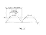
- FIG. 2 is a graph illustrating a criterion for a power conversion operation of a power supply apparatus according to an embodiment of the present invention.
- FIGS. 3 and 5 are graphs showing operating waveforms of a power supply apparatus according to an embodiment of the present invention.
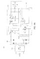
- FIGS. 4A through 4C are views showing a flow of a current in the case illustrated in FIG. 3 .
- FIGS. 6A and 6B are views showing a flow of a current in the case illustrated in FIG. 5 .
- the forward converter unit 110 may selectively perform the power conversion operation according to a comparison result between the voltage levels of input power Vin and output power Vo. In the case in which the voltage level of the input power is higher than that of the output power, the forward converter unit 110 may perform the power conversion operation, and in the case in which the voltage level of the input power is lower than that of the output power, the forward converter unit 110 may stop the power conversion operation.
- the forward converter unit 110 may perform the power conversion operation. Referring to FIGS. 3 and FIGS. 4A to 4C , at the time of turn-off of the power switch Q, an input voltage Vin is larger than voltage VOR induced to the primary side of the transformer. In addition, in a turn-off section of the power switch Q, a current of the primary side of the transformer is reset toward the output voltage through the second secondary winding C.
- an operational range of this section is increased, such that a current peak value of a current iLm of a magnetizing inductor Lm is decreased, thereby decreasing overall core loss.
- an inductor-capacitor (L-C) Lo and Co structure of an output terminal of the forward converter unit may also be used as an output filter, such that an output voltage ripple in the turn-off section of the power switch Q may be decreased.
- Mode 1 (t0 ⁇ t1): In this section, the power switch Q is turned on, and a conduction path as illustrated in a solid line of FIG. 3A is formed. In this section, the forward converter unit 110 performs the power conversion operation. Therefore, in this section, an output diode Do1 is conducted, and stored energy of a circuit is transferred to an output load through a transformer and an output inductor Lo. In addition, a certain amount of energy is stored in the magnetizing inductor Lm. Here, a current flowing in the magnetizing inductor Lm is increased at a gradient of Vin/Lm. A current flowing in the output diode Do1 is the same as a current flowing in the output inductor Lo.
- the current flowing in the output inductor Lo may be represented by the following Equation 1.
- i Lo t 1 L o ⁇ N s N p ⁇ V in - V o ⁇ t
- Output diodes Do2 and Do3 are not conducted, such that a current does not flow in the output diodes Do2 and Do3. At this time, voltages applied to the diodes become Ns*Vin/Np and Nc*Vin/Np+Vo, respectively.
- Mode 2 (t1 ⁇ t2): In this section, the power switch Q starts to be turned off, and a conduction path as illustrated in a solid line of FIG. 4B is formed.
- the current iLm that has flowed in the magnetizing inductor of the primary side in the previous mode flows in the second secondary winding C for reset, such that the output diode Do3 is conducted.
- the current flowing in the output diode Do3 may be represented by the following Equation 2 and the current flowing in the output diode Do3 flows to a section of Mode 3 in which the current iLm of the magnetizing inductor of the primary side becomes ⁇ 0'.
- i Do ⁇ 3 t - V o L m ⁇ N p N c 2 ⁇ t
- an output of the forward converter unit 110 is as follows: the output diode Do2 is conducted, such that a current flows through the same path as the output inductor Lo and has a gradient of -Vo/Lo. A voltage applied across the output inductor Lo is the same as the output voltage. In this case, when the current becomes '0', Mode 2 ends.
- Mode 3 (t2 ⁇ t3): After the power switch Q is turned off, the current that has flowed in the output diode Do2 and the output inductor Lo of the forward converter unit 110 becomes '0', and a conduction path as illustrated in a solid line of FIG. 4C is formed. The current that has been reset from the previous section flows through the output diode Do3. In this case, when the current iLm of the magnetizing inductor of the primary side becomes '0', the current of the output diode Do3 also becomes '0', such that Mode 3 ends. At this time, the power switch Q is turned on.
- only the flyback converter unit 120 may perform the power conversion operation. Referring to FIGS. 5 and FIGS. 6A and 6B , in the case in which the voltage level of the input power is lower than that of the power induced to the primary side of the transformer, only the flyback converter unit 120 may be operated, and the forward converter unit 110 may not be operated.
- the flyback converter unit 120 may be divided into Modes 1 and 2 corresponding to two sections, which are a turn-on section and a turn-off section of a switch, as illustrated in FIG. 5 .
- Mode 1 (t0 ⁇ t1): In this section, the power switch Q is turned on, and a conduction path as illustrated in a solid line of FIG. 6A is formed. In this section, there is no conducted diode, and a current does not flow, even in the output inductor Lo.
- Voltages applied across the output diodes Do1, Do2, and Do3 are Ns*Vin/Np, Vout, and Nc*Vin/Np+Vout, respectively, that is, Ns*Vin/Np applied to the output diode Do1, Vout applied to the output diode Do2, and Nc*Vin/Np+Vout applied to the output diode Do3.
- the output diode Do2 always has a voltage stress of Vout, Vout being an output voltage in a section in which Vin ⁇ VOR.
- Mode 2 (t1 ⁇ t2): In this section, the power switch Q is turned off, and a conduction path as illustrated in a solid line of FIG. 6B is formed.
- a voltage stress of Np*Vo/Nc+Vin is applied to the power switch Q.
- a voltage of -Np*Vo/Nc is applied to the primary side, and the current iLm flowing in the magnetizing inductor is transferred to a secondary side flyback output through the primary side transformer. Therefore, the output diode Do3 is conducted and the current flowing in the output diode Do3 has the same gradient as that of the above Equation 2.
- the output diode Do2 has a voltage stress of Vout as in the turn-on section of the power switch Q, and the output diode Do1 has a voltage stress of (1+Ns/Nc)Vout.
- the current flowing in the output diode Do3 of the second secondary winding C becomes 0, the turn-on section of the power switch Q starts.
- FIGS. 7A and 7B are graphs showing operating waveforms according to a voltage level of input power.
- the power supply apparatus in the case in which the voltage level of the input power Vin is 100 Vrms, the power supply apparatus according to the embodiment of the present invention may be operated in the same scheme as that of a flyback converter in a general BCM mode.
- the forward converter unit 110 also performs the power conversion operation and the current iLo of the output inductor is operated in a discontinuous conduction mode (DCM), in a section in which Vin>VOR, as illustrated in FIG. 7B .
- DCM discontinuous conduction mode
- the power factor correction function and the constant current control are performed in a single circuit stage, such that the power conversion efficiency is increased and a dead zone of the input power is removed, whereby the power factor may be increased.
- the flyback converter performing an existing power factor improving function has a more simple circuit configuration and slightly higher efficiency (a maximum efficiency of about 88%) as compared with an LED driving circuit including a power factor correction circuit and a DC to DC converter. That is, power consumption of a snubber, power consumption of a transformer core, and power consumption of a primary side power switch tend to be illustrated to be slightly large.
- the current of the magnetizing inductor of the transformer is reset toward the output in order to significantly increase the efficiency by improving the defects described above, such that powering may be obtained in the entire section Ts of one period.
- a root mean square (RMS) of the current of the primary side is decreased, such that conduction loss may be decreased.
- offset of the current of the magnetizing inductor is relatively small, such that transformer core loss is decreased, whereby high efficiency may be accomplished.
- the second secondary winding side is configured in a flyback form, such that it is operated as the flyback converter in the case in which the input voltage is lower than the output voltage, and is operated as the flyback converter and the forward converter in the case in which the input voltage is higher than the output voltage. Therefore, the power factor may be increased without the dead zone of the input current, and the core loss is decreased as compared to the flyback converter according to the related art, such that efficiency may be improved.
Landscapes
- Engineering & Computer Science (AREA)
- Power Engineering (AREA)
- Dc-Dc Converters (AREA)
Abstract
There are provided a single stage forward-flyback converter, and a power supply apparatus capable of increasing power factor correction and power conversion efficiency. The single stage forward-flyback converter includes: a forward converter unit including a transformer having a primary winding receiving input power and a first secondary winding magnetically coupled to the primary winding to receive power induced thereto, and converting the power in a forward scheme; and a flyback converter unit sharing the transformer, including a second secondary winding, and converting the power in a flyback scheme, wherein the forward converter unit is selectively operated according to a voltage level of the input power.
Description
- This application claims the priorities of Korean Patent Application Nos.
10-2012-0085171 filed on August 3, 2012 10-2013-0089659 filed on July 29, 2013 - The present invention relates to a single stage forward-flyback converter, and a power supply apparatus.
- Generally, in order to drive an electronic device domestically, commercially or industrially, a power supply apparatus converting commercially available power into driving power appropriate for the electronic device and supplying the converted driving power thereto, is used inside or outside the electronic device.
- The power supply apparatus may also be used in order to drive a light emitting diode.
- Recently, interest in and demand for a light emitting diode (LED) has increased.
- A device using a light emitting diode may be manufactured to be compact to thereby be used in a situation in which it is difficult to install an existing electronic product. Further, in the case in which a light emitting diode is used as an illumination apparatus, it is easy to implement various colors of light and control illuminance levels, such that a light emitting diode may be used as a system illumination apparatus appropriate for devices used in situations such as watching movies, reading, conferencing, or the like.
- In addition, a light emitting diode consumes approximately 1/8 of the power consumed by an incandescent lamp, has a lifespan of fifty thousand to one hundred thousand hours, 5 to 10 times longer than that of an incandescent lamp, and is an environmentally-friendly, mercury free light source and may be variously implemented.
- Due to these characteristics, light emitting diode illumination projects have been implemented as government-supported projects in many nations, such as America, Japan, Australia, and others, as well as Korea.
- As described above, a light emitting diode, the use of which has increased, requires a driving apparatus for the driving thereof. However, as described in the following Related Art Document, in the case in which a two-stage configuration is applied to a power factor correction circuit stage performing power factor correction and a direct current (DC) to DC converter circuit stage for constant current control of an output load, power conversion efficiency may be deteriorated, and in the case of driving a plurality of light emitting diode arrays, when a required light emitting diode driving voltage rises, manufacturing costs may be increased due to the use of a high voltage element.
- Korean Patent Laid-open Publication No.
2012-0031215 - An aspect of the present invention provides a single stage forward-flyback converter, and a power supply apparatus capable of increasing power factor correction and power conversion efficiency while performing a power factor correction function and a constant current control in a single circuit stage.
- According to an aspect of the present invention, there is provided a single stage forward-flyback converter including: a forward converter unit including a transformer having a primary winding receiving input power and a first secondary winding magnetically coupled to the primary winding to receive power induced thereto, and converting the power in a forward scheme; and a flyback converter unit sharing the transformer with the forward converter unit, including a second secondary winding provided in the transformer and magnetically coupled to the primary winding, and converting the power in a flyback scheme, wherein the forward converter unit is selectively operated according to a voltage level of the input power.
- The forward converter unit may perform a power conversion operation in a case in which the voltage level of the input power is higher than that of output power of the single stage forward-flyback converter.
- The flyback converter unit may perform the power conversion operation regardless of the voltage level of the input power.
- The forward converter unit and the flyback converter unit may share a power switch switching the power input to the primary winding of the transformer.
- The power switch may continually maintain a turn-on duty to improve a power factor of the input power.
- The input power may be rectified and then transferred to the primary winding.
- Winding start points of the primary winding and the first secondary winding may be formed in the same position as each other.
- Winding start points of the primary winding and the second secondary winding may be formed in positions opposing each other.
- Outputs of the forward converter unit and the flyback converter unit may be supplied to at least one light emitting diode.
- According to another aspect of the present invention, there is provided a power supply apparatus including: a rectifying unit rectifying alternating current (AC) power; a forward converter unit including a transformer having a primary winding receiving the rectified power from the rectifying unit and a first secondary winding magnetically coupled to the primary winding to receive power induced thereto, and converting the power in a forward scheme; and a flyback converter unit sharing the transformer with the forward converter unit, including a second secondary winding provided in the transformer and magnetically coupled to the primary winding, and converting the power in a flyback scheme, wherein the forward converter unit is selectively operated according to a voltage level of the rectified power.
- The forward converter unit may perform a power conversion operation in a case in which the voltage level of the rectified power is higher than that of power induced from output power of the power supply apparatus to the primary winding of the transformer.
- The flyback converter unit may perform the power conversion operation regardless of the voltage level of the AC power.
- The power supply apparatus may further include an electromagnetic interference (EMI) filter removing EMI of the AC power.
- The above and other aspects, features and other advantages of the present invention will be more clearly understood from the following detailed description taken in conjunction with the accompanying drawings, in which:
-
FIG. 1 is a schematic circuit diagram of a power supply apparatus according to an embodiment of the present invention; -
FIG. 2 is a graph illustrating a criterion for a power conversion operation of a power supply apparatus according to an embodiment of the present invention; -
FIGS. 3 and5 are graphs showing operating waveforms of a power supply apparatus according to an embodiment of the present invention; -
FIGS. 4A through 4C are views showing a flow of a current in the case illustrated inFIG. 3 ; -
FIGS. 6A and6B are views showing a flow of a current in the case illustrated inFIG. 5 ; and -
FIGS. 7A and7B are graphs showing operating waveforms according to a voltage level of input power. - Hereinafter, embodiments of the present invention will be described in detail with reference to the accompanying drawings. The invention may, however, be embodied in many different forms and should not be construed as being limited to the embodiments set forth herein. Rather, these embodiments are provided so that this disclosure will be thorough and complete, and will fully convey the scope of the invention to those skilled in the art.
- In the drawings, the shapes and dimensions of elements may be exaggerated for clarity, and the same reference numerals will be used throughout to designate the same or like elements.
- A case in which any one part is connected to the other part includes a case in which the parts are directly connected to each other and a case in which the parts are indirectly connected to each other with other elements interposed therebetween.
- In addition, unless explicitly described otherwise, "comprising" any components will be understood to imply the inclusion of other components but not the exclusion of any other components.
-
FIG. 1 is a schematic circuit diagram of a power supply apparatus according to an embodiment of the present invention. - Referring to
FIG. 1 , thepower supply apparatus 100 according to the embodiment of the present invention may include aforward converter unit 110 and aflyback converter unit 120. In addition, thepower supply apparatus 100 according to the embodiment of the present invention may further include a controlling unit 130, an electromagnetic interference (EMI)filter 140, and a rectifyingunit 150. - The
forward converter unit 110 and theflyback converter unit 120 may share a primary winding P of the transformer and a power switch Q with each other. - The
forward converter unit 110 may include a transformer having the primary winding P and a first secondary winding S and the power switch Q switching power input to the primary winding P. The primary winding P and the first secondary winding S may be magnetically coupled to each other so as to have a preset turns ratio, the power input to the primary winding P may induce power to the first secondary winding S according to the switching of the power switch Q, and a voltage level of the power induced to the first secondary winding S may be determined according to the turns ratio. - Since the
forward converter unit 110 performs a power conversion operation in a forward scheme, winding start points of the primary winding P and the first secondary winding S may be formed in the same position as each other. - The
flyback converter unit 120 may share the transformer and the power switch Q with theforward converter unit 110, and the transformer may have a second secondary winding C. The second secondary winding C may be magnetically coupled to the primary winding P to have a preset turns ratio, the power input to the primary winding P may induce power to the second secondary winding C according to the switching of the power switch Q, and a voltage level of the power induced to the second secondary winding C may be determined according to the turns ratio. - Since the
flyback converter unit 120 performs a power conversion operation in a flyback scheme, winding start points of the primary winding P and the second secondary winding C may be formed in positions opposing each other. - Output power of the
forward converter unit 110 and theflyback converter unit 120 may be transferred to a load Ro, particularly, at least one light emitting diode (LED) to allow the LED to perform a light emitting operation. A plurality of LEDs may be connected in series with each other to configure a single LED array. Although not illustrated, a plurality of LED arrays may be connected to each other in parallel and receive the output power to perform a light emitting operation. - The
EMI filter 140 may filter electromagnetic interference (EMI) from input AC power, and the rectifyingunit 150 may rectify the filtered power and transfer the rectified filtered power to the primary winding P of the transformer. - The
forward converter unit 110 may selectively perform a power conversion operation according to a voltage level of the input power. More specifically, theforward converter unit 110 may perform the power conversion operation in the case in which the voltage level of the input power is higher than that of the output power. - Meanwhile, the
flyback converter unit 120 may perform a power conversion operation regardless of the voltage level of the input power. - In addition, the
forward converter unit 110 and theflyback converter unit 120 may share the power switch Q, wherein the power switch Q may continually maintain a turn-on duty to improve a power factor of the input power. - That is, the
forward converter unit 110 and theflyback converter unit 120 may perform power factor improvement and power conversion operations in a single power conversion circuit. - Hereinafter, selective power conversion operations of the
forward converter unit 110 and theflyback converter unit 120 according to a comparison between voltage levels of the input power and the output power will be described in detail. -
FIG. 2 is a graph illustrating a criterion for a power conversion operation of a power supply apparatus according to an embodiment of the present invention.FIGS. 3 and5 are graphs showing operating waveforms of a power supply apparatus according to an embodiment of the present invention.FIGS. 4A through 4C are views showing a flow of a current in the case illustrated inFIG. 3 .FIGS. 6A and6B are views showing a flow of a current in the case illustrated inFIG. 5 . - With reference to
FIG. 2 , as described above, theforward converter unit 110 may selectively perform the power conversion operation according to a comparison result between the voltage levels of input power Vin and output power Vo. In the case in which the voltage level of the input power is higher than that of the output power, theforward converter unit 110 may perform the power conversion operation, and in the case in which the voltage level of the input power is lower than that of the output power, theforward converter unit 110 may stop the power conversion operation. - In the case in which the voltage level of the input power is higher than that of the output power, the
forward converter unit 110 may perform the power conversion operation. Referring toFIGS. 3 andFIGS. 4A to 4C , at the time of turn-off of the power switch Q, an input voltage Vin is larger than voltage VOR induced to the primary side of the transformer. In addition, in a turn-off section of the power switch Q, a current of the primary side of the transformer is reset toward the output voltage through the second secondary winding C. - Further, as the input voltage is increased, an operational range of this section is increased, such that a current peak value of a current iLm of a magnetizing inductor Lm is decreased, thereby decreasing overall core loss. When the power switch Q is turned off, an inductor-capacitor (L-C) Lo and Co structure of an output terminal of the forward converter unit may also be used as an output filter, such that an output voltage ripple in the turn-off section of the power switch Q may be decreased.
-
Modes 1 to 3 set each time, as illustrated in the graph ofFIG. 3 , will be described in detail. - Mode 1 (t0∼t1): In this section, the power switch Q is turned on, and a conduction path as illustrated in a solid line of
FIG. 3A is formed. In this section, theforward converter unit 110 performs the power conversion operation. Therefore, in this section, an output diode Do1 is conducted, and stored energy of a circuit is transferred to an output load through a transformer and an output inductor Lo. In addition, a certain amount of energy is stored in the magnetizing inductor Lm. Here, a current flowing in the magnetizing inductor Lm is increased at a gradient of Vin/Lm. A current flowing in the output diode Do1 is the same as a current flowing in the output inductor Lo. In this section, since the current flowing in the output inductor Lo is not present, an initial current value of the output inductor Lo is '0'. The current flowing in the output inductor Lo may be represented by the followingEquation 1.
- Output diodes Do2 and Do3 are not conducted, such that a current does not flow in the output diodes Do2 and Do3. At this time, voltages applied to the diodes become Ns*Vin/Np and Nc*Vin/Np+Vo, respectively.
- Mode 2 (t1∼t2): In this section, the power switch Q starts to be turned off, and a conduction path as illustrated in a solid line of
FIG. 4B is formed. The current iLm that has flowed in the magnetizing inductor of the primary side in the previous mode flows in the second secondary winding C for reset, such that the output diode Do3 is conducted. The current flowing in the output diode Do3 may be represented by the followingEquation 2 and the current flowing in the output diode Do3 flows to a section ofMode 3 in which the current iLm of the magnetizing inductor of the primary side becomes `0'.
- Further, in this section, an output of the
forward converter unit 110 is as follows: the output diode Do2 is conducted, such that a current flows through the same path as the output inductor Lo and has a gradient of -Vo/Lo. A voltage applied across the output inductor Lo is the same as the output voltage. In this case, when the current becomes '0',Mode 2 ends. - Mode 3 (t2∼t3): After the power switch Q is turned off, the current that has flowed in the output diode Do2 and the output inductor Lo of the
forward converter unit 110 becomes '0', and a conduction path as illustrated in a solid line ofFIG. 4C is formed. The current that has been reset from the previous section flows through the output diode Do3. In this case, when the current iLm of the magnetizing inductor of the primary side becomes '0', the current of the output diode Do3 also becomes '0', such thatMode 3 ends. At this time, the power switch Q is turned on. - In the case in which the voltage level of the input power is lower than that of the output power, only the
flyback converter unit 120 may perform the power conversion operation. Referring toFIGS. 5 andFIGS. 6A and6B , in the case in which the voltage level of the input power is lower than that of the power induced to the primary side of the transformer, only theflyback converter unit 120 may be operated, and theforward converter unit 110 may not be operated. - In the case in which only the
flyback converter unit 120 is operated, it may be divided intoModes FIG. 5 . - Mode 1 (t0∼t1): In this section, the power switch Q is turned on, and a conduction path as illustrated in a solid line of
FIG. 6A is formed. In this section, there is no conducted diode, and a current does not flow, even in the output inductor Lo. Voltages applied across the output diodes Do1, Do2, and Do3 are Ns*Vin/Np, Vout, and Nc*Vin/Np+Vout, respectively, that is, Ns*Vin/Np applied to the output diode Do1, Vout applied to the output diode Do2, and Nc*Vin/Np+Vout applied to the output diode Do3. Here, the output diode Do2 always has a voltage stress of Vout, Vout being an output voltage in a section in which Vin<VOR. - Mode 2 (t1∼t2): In this section, the power switch Q is turned off, and a conduction path as illustrated in a solid line of
FIG. 6B is formed. When the power switch Q is turned off, a voltage stress of Np*Vo/Nc+Vin is applied to the power switch Q. At this time, a voltage of -Np*Vo/Nc is applied to the primary side, and the current iLm flowing in the magnetizing inductor is transferred to a secondary side flyback output through the primary side transformer. Therefore, the output diode Do3 is conducted and the current flowing in the output diode Do3 has the same gradient as that of theabove Equation 2. - The output diode Do2 has a voltage stress of Vout as in the turn-on section of the power switch Q, and the output diode Do1 has a voltage stress of (1+Ns/Nc)Vout. When the current flowing in the output diode Do3 of the second secondary winding C becomes 0, the turn-on section of the power switch Q starts.
-
FIGS. 7A and7B are graphs showing operating waveforms according to a voltage level of input power. - First, main operating waveforms in the case in which the voltage level of the input power Vin is 100Vrms are illustrated in
FIG. 6A . It can be confirmed that output specifications are controlled to be appropriate for 42V and 570mA and a boundary conduction mode (BCM) operation is performed. In addition, since a turns ratio between the primary winding P and the first secondary winding S is 3:1, in the case in which the voltage level of the input power Vin is 100Vrms, Vin is always smaller than VOR, such that only theflyback converter unit 120 may be operated, theforward converter unit 110 may not be operated, and the current flowing in the output inductor Lo becomes `0'. That is, in the case in which the voltage level of the input power Vin is 100 Vrms, the power supply apparatus according to the embodiment of the present invention may be operated in the same scheme as that of a flyback converter in a general BCM mode. On the other hand, it could be confirmed that in the case in which the voltage level of the input power Vin is 260 Vrms, theforward converter unit 110 also performs the power conversion operation and the current iLo of the output inductor is operated in a discontinuous conduction mode (DCM), in a section in which Vin>VOR, as illustrated inFIG. 7B . - As set forth above, according to the embodiments of the present invention, the power factor correction function and the constant current control are performed in a single circuit stage, such that the power conversion efficiency is increased and a dead zone of the input power is removed, whereby the power factor may be increased.
- That is, the flyback converter performing an existing power factor improving function has a more simple circuit configuration and slightly higher efficiency (a maximum efficiency of about 88%) as compared with an LED driving circuit including a power factor correction circuit and a DC to DC converter. That is, power consumption of a snubber, power consumption of a transformer core, and power consumption of a primary side power switch tend to be illustrated to be slightly large. In the embodiment of the present invention, the current of the magnetizing inductor of the transformer is reset toward the output in order to significantly increase the efficiency by improving the defects described above, such that powering may be obtained in the entire section Ts of one period. Thus, a root mean square (RMS) of the current of the primary side is decreased, such that conduction loss may be decreased. In addition, offset of the current of the magnetizing inductor is relatively small, such that transformer core loss is decreased, whereby high efficiency may be accomplished.
- In an existing forward converter, in the case in which the input voltage is lower than the output voltage, since powering to the output side is not obtained, a dead zone of the input current is generated, such that it is difficult to expect a high power factor improvement effect. However, in the embodiment of the present invention, the second secondary winding side is configured in a flyback form, such that it is operated as the flyback converter in the case in which the input voltage is lower than the output voltage, and is operated as the flyback converter and the forward converter in the case in which the input voltage is higher than the output voltage. Therefore, the power factor may be increased without the dead zone of the input current, and the core loss is decreased as compared to the flyback converter according to the related art, such that efficiency may be improved.
- While the present invention has been illustrated and described in connection with the embodiments, it will be apparent to those skilled in the art that modifications and variations can be made without departing from the spirit and scope of the invention as defined by the appended claims.
Claims (15)
- A single stage forward-flyback converter comprising:a forward converter unit including a transformer having a primary winding receiving input power and a first secondary winding magnetically coupled to the primary winding to receive power induced thereto, and converting the power in a forward scheme; anda flyback converter unit sharing the transformer with the forward converter unit, including a second secondary winding provided in the transformer and magnetically coupled to the primary winding, and converting the power in a flyback scheme,the forward converter unit being selectively operated according to a voltage level of the input power.
- The single stage forward-flyback converter of claim 1, wherein the forward converter unit performs a power conversion operation in a case in which the voltage level of the input power is higher than that of output power of the single stage forward-flyback converter.
- The single stage forward-flyback converter of claim 1, wherein the flyback converter unit performs the power conversion operation regardless of the voltage level of the input power.
- The single stage forward-flyback converter of claim 1, wherein the forward converter unit and the flyback converter unit share a power switch switching the power input to the primary winding of the transformer.
- The single stage forward-flyback converter of claim 1, wherein the power switch continually maintains a turn-on duty to improve a power factor of the input power.
- The single stage forward-flyback converter of claim 1, wherein the input power is rectified and then transferred to the primary winding.
- The single stage forward-flyback converter of claim 1, wherein winding start points of the primary winding and the first secondary winding are formed in the same position as each other.
- The single stage forward-flyback converter of claim 1, wherein winding start points of the primary winding and the second secondary winding are formed in positions opposing each other.
- The single stage forward-flyback converter of claim 1, wherein outputs of the forward converter unit and the flyback converter unit are supplied to at least one light emitting diode.
- A power supply apparatus comprising:a rectifying unit rectifying alternating current (AC) power;a forward converter unit including a transformer having a primary winding receiving the rectified power from the rectifying unit and a first secondary winding magnetically coupled to the primary winding to receive power induced thereto, and converting the power in a forward scheme; anda flyback converter unit sharing the transformer with the forward converter unit, including a second secondary winding provided in the transformer and magnetically coupled to the primary winding, and converting the power in a flyback scheme,the forward converter unit being selectively operated according to a voltage level of the rectified power.
- The power supply apparatus of claim 10, wherein the forward converter unit performs a power conversion operation in a case in which the voltage level of the rectified power is higher than that of output power of the power supply apparatus.
- The power supply apparatus of claim 10, wherein the flyback converter unit performs the power conversion operation regardless of the voltage level of the rectified power.
- The power supply apparatus of claim 10, wherein the forward converter unit and the flyback converter unit share a power switch switching the power input to the primary winding of the transformer.
- The power supply apparatus of claim 13, wherein the power switch continually maintains a turn-on duty to improve a power factor of the rectified power.
- The power supply apparatus of claim 10, wherein winding start points of the primary winding and the first secondary winding are formed in the same position as each other.
Applications Claiming Priority (2)
| Application Number | Priority Date | Filing Date | Title |
|---|---|---|---|
| KR20120085171 | 2012-08-03 | ||
| KR1020130089659A KR101496819B1 (en) | 2012-08-03 | 2013-07-29 | Single stage forward-flyback converter, power supplying apparatus and power suppying apparatus for light emitting diode |
Publications (1)
| Publication Number | Publication Date |
|---|---|
| EP2693620A2 true EP2693620A2 (en) | 2014-02-05 |
Family
ID=48915946
Family Applications (1)
| Application Number | Title | Priority Date | Filing Date |
|---|---|---|---|
| EP13275178.5A Withdrawn EP2693620A2 (en) | 2012-08-03 | 2013-07-31 | Single stage forward-flyback converter and power supply apparatus |
Country Status (2)
| Country | Link |
|---|---|
| US (1) | US20140035477A1 (en) |
| EP (1) | EP2693620A2 (en) |
Cited By (1)
| Publication number | Priority date | Publication date | Assignee | Title |
|---|---|---|---|---|
| CN105515397A (en) * | 2016-02-05 | 2016-04-20 | 航天长峰朝阳电源有限公司 | Double-excitation synchronous non-inductive rectifying circuit |
Families Citing this family (4)
| Publication number | Priority date | Publication date | Assignee | Title |
|---|---|---|---|---|
| EP2693619A2 (en) * | 2012-08-03 | 2014-02-05 | Samsung Electro-Mechanics Co., Ltd | Single stage forward-flyback converter and power supply apparatus |
| CN104507198B (en) * | 2014-11-12 | 2017-11-07 | 瑞芙贝(武汉)光电科技发展有限公司 | Active clamping forward, flyback recommend integrated lamp controller |
| WO2019082018A1 (en) * | 2017-10-27 | 2019-05-02 | Silanna Asia Pte Ltd | Merged voltage-divider forward converter |
| CN119276120A (en) | 2023-07-05 | 2025-01-07 | 财团法人工业技术研究院 | Forward converter and forward power factor corrector |
Family Cites Families (12)
| Publication number | Priority date | Publication date | Assignee | Title |
|---|---|---|---|---|
| US5126931A (en) * | 1990-09-07 | 1992-06-30 | Itt Corporation | Fixed frequency single ended forward converter switching at zero voltage |
| US5434768A (en) * | 1993-02-12 | 1995-07-18 | Rompower | Fixed frequency converter switching at zero voltage |
| US5982638A (en) * | 1997-10-31 | 1999-11-09 | Astec International Limited | Single stage power converter with regenerative snubber and power factor correction |
| US6069801A (en) * | 1998-07-16 | 2000-05-30 | Vlt Corporation | Power factor correction in switching power conversion |
| US6304065B1 (en) * | 2001-03-02 | 2001-10-16 | Technical Witts, Inc. | Power electronic circuits with all terminal currents non-pulsating |
| WO2004038900A2 (en) * | 2002-10-21 | 2004-05-06 | Advanced Power Technology, Inc. | Ac-dc power converter having high input power factor and low harmonic distortion |
| JP4238871B2 (en) * | 2004-01-30 | 2009-03-18 | 株式会社村田製作所 | Switching power supply |
| US7902771B2 (en) * | 2006-11-21 | 2011-03-08 | Exclara, Inc. | Time division modulation with average current regulation for independent control of arrays of light emitting diodes |
| US8693213B2 (en) * | 2008-05-21 | 2014-04-08 | Flextronics Ap, Llc | Resonant power factor correction converter |
| US8643222B2 (en) * | 2009-06-17 | 2014-02-04 | Power Systems Technologies Ltd | Power adapter employing a power reducer |
| US8638578B2 (en) * | 2009-08-14 | 2014-01-28 | Power System Technologies, Ltd. | Power converter including a charge pump employable in a power adapter |
| CN102870320B (en) * | 2010-03-17 | 2016-11-02 | 电力系统技术有限公司 | The control system of power converter and operational approach thereof |
-
2013
- 2013-07-31 EP EP13275178.5A patent/EP2693620A2/en not_active Withdrawn
- 2013-08-02 US US13/957,808 patent/US20140035477A1/en not_active Abandoned
Cited By (1)
| Publication number | Priority date | Publication date | Assignee | Title |
|---|---|---|---|---|
| CN105515397A (en) * | 2016-02-05 | 2016-04-20 | 航天长峰朝阳电源有限公司 | Double-excitation synchronous non-inductive rectifying circuit |
Also Published As
| Publication number | Publication date |
|---|---|
| US20140035477A1 (en) | 2014-02-06 |
Similar Documents
| Publication | Publication Date | Title |
|---|---|---|
| Lee et al. | A single-switch AC–DC LED driver based on a boost-flyback PFC converter with lossless snubber | |
| Moo et al. | An efficient driver for dimmable LED lighting | |
| KR100950913B1 (en) | Power converter | |
| Zhang et al. | A precise passive current balancing method for multioutput LED drivers | |
| KR102098223B1 (en) | Multiple output dc/dc converter and power supply having the same | |
| US8385089B2 (en) | Multiple-output switching power supply unit | |
| JP5736772B2 (en) | Constant current power supply | |
| WO2013128506A1 (en) | Dc power supply circuit | |
| US20150303813A1 (en) | Ac-to-dc power converting device | |
| US7440294B2 (en) | Power adapter and power supply system using the same | |
| TWI516007B (en) | DC power supply unit | |
| US20140035477A1 (en) | Single stage forward-flyback converter and power supply apparatus | |
| JP2007174793A (en) | Multiple output switching power supply | |
| JP5910814B2 (en) | Power converter | |
| Graziani et al. | Isolated flying capacitor multilevel converters | |
| KR101496819B1 (en) | Single stage forward-flyback converter, power supplying apparatus and power suppying apparatus for light emitting diode | |
| WO2013128509A1 (en) | Dc power supply circuit | |
| KR101434110B1 (en) | Single stage forward-flyback converter, power supplying apparatus and power suppying apparatus for light emitting diode | |
| EP2693619A2 (en) | Single stage forward-flyback converter and power supply apparatus | |
| US9030128B2 (en) | LED drive circuit | |
| US9450495B2 (en) | Single stage forward-flyback converter and power supply apparatus for light emitting diode | |
| US20140268910A1 (en) | Coupled inductor dc step down converter | |
| JP5551995B2 (en) | Power supply device and lighting device provided with the power supply device | |
| JP2016123195A (en) | Non-insulated power supply | |
| Zawawi et al. | A single-stage power factor corrected LED driver with dual half-wave rectifier |
Legal Events
| Date | Code | Title | Description |
|---|---|---|---|
| 17P | Request for examination filed |
Effective date: 20130731 |
|
| AK | Designated contracting states |
Kind code of ref document: A2 Designated state(s): AL AT BE BG CH CY CZ DE DK EE ES FI FR GB GR HR HU IE IS IT LI LT LU LV MC MK MT NL NO PL PT RO RS SE SI SK SM TR |
|
| AX | Request for extension of the european patent |
Extension state: BA ME |
|
| PUAI | Public reference made under article 153(3) epc to a published international application that has entered the european phase |
Free format text: ORIGINAL CODE: 0009012 |
|
| STAA | Information on the status of an ep patent application or granted ep patent |
Free format text: STATUS: THE APPLICATION HAS BEEN WITHDRAWN |
|
| 18W | Application withdrawn |
Effective date: 20160120 |