EP2693239A1 - Optical element, headup display, and method for manufacturing optical element - Google Patents
Optical element, headup display, and method for manufacturing optical element Download PDFInfo
- Publication number
- EP2693239A1 EP2693239A1 EP20110793998 EP11793998A EP2693239A1 EP 2693239 A1 EP2693239 A1 EP 2693239A1 EP 20110793998 EP20110793998 EP 20110793998 EP 11793998 A EP11793998 A EP 11793998A EP 2693239 A1 EP2693239 A1 EP 2693239A1
- Authority
- EP
- European Patent Office
- Prior art keywords
- microlens array
- microlens
- array unit
- lens
- optical element
- Prior art date
- Legal status (The legal status is an assumption and is not a legal conclusion. Google has not performed a legal analysis and makes no representation as to the accuracy of the status listed.)
- Granted
Links
- 230000003287 optical effect Effects 0.000 title claims abstract description 69
- 238000000034 method Methods 0.000 title claims description 17
- 238000004519 manufacturing process Methods 0.000 title claims description 14
- 238000012986 modification Methods 0.000 description 50
- 230000004048 modification Effects 0.000 description 50
- 238000003491 array Methods 0.000 description 17
- 238000010586 diagram Methods 0.000 description 11
- 230000000052 comparative effect Effects 0.000 description 7
- 230000000694 effects Effects 0.000 description 7
- 230000015654 memory Effects 0.000 description 4
- 238000007796 conventional method Methods 0.000 description 3
- 239000004065 semiconductor Substances 0.000 description 3
- 239000002131 composite material Substances 0.000 description 2
- RKTYLMNFRDHKIL-UHFFFAOYSA-N copper;5,10,15,20-tetraphenylporphyrin-22,24-diide Chemical compound [Cu+2].C1=CC(C(=C2C=CC([N-]2)=C(C=2C=CC=CC=2)C=2C=CC(N=2)=C(C=2C=CC=CC=2)C2=CC=C3[N-]2)C=2C=CC=CC=2)=NC1=C3C1=CC=CC=C1 RKTYLMNFRDHKIL-UHFFFAOYSA-N 0.000 description 2
- 238000002474 experimental method Methods 0.000 description 2
- ZZUFCTLCJUWOSV-UHFFFAOYSA-N furosemide Chemical compound C1=C(Cl)C(S(=O)(=O)N)=CC(C(O)=O)=C1NCC1=CC=CO1 ZZUFCTLCJUWOSV-UHFFFAOYSA-N 0.000 description 2
- 230000001629 suppression Effects 0.000 description 2
- 239000000853 adhesive Substances 0.000 description 1
- 230000001070 adhesive effect Effects 0.000 description 1
- 238000006243 chemical reaction Methods 0.000 description 1
- 238000013461 design Methods 0.000 description 1
- 230000005484 gravity Effects 0.000 description 1
- 239000004973 liquid crystal related substance Substances 0.000 description 1
- 239000011347 resin Substances 0.000 description 1
- 229920005989 resin Polymers 0.000 description 1
- 230000001360 synchronised effect Effects 0.000 description 1
- 230000003936 working memory Effects 0.000 description 1
Images






Classifications
-
- G—PHYSICS
- G02—OPTICS
- G02B—OPTICAL ELEMENTS, SYSTEMS OR APPARATUS
- G02B3/00—Simple or compound lenses
- G02B3/0006—Arrays
- G02B3/0037—Arrays characterized by the distribution or form of lenses
- G02B3/0056—Arrays characterized by the distribution or form of lenses arranged along two different directions in a plane, e.g. honeycomb arrangement of lenses
-
- G—PHYSICS
- G02—OPTICS
- G02B—OPTICAL ELEMENTS, SYSTEMS OR APPARATUS
- G02B27/00—Optical systems or apparatus not provided for by any of the groups G02B1/00 - G02B26/00, G02B30/00
- G02B27/01—Head-up displays
- G02B27/0101—Head-up displays characterised by optical features
-
- G—PHYSICS
- G02—OPTICS
- G02B—OPTICAL ELEMENTS, SYSTEMS OR APPARATUS
- G02B3/00—Simple or compound lenses
- G02B3/0006—Arrays
- G02B3/0037—Arrays characterized by the distribution or form of lenses
- G02B3/0062—Stacked lens arrays, i.e. refractive surfaces arranged in at least two planes, without structurally separate optical elements in-between
- G02B3/0068—Stacked lens arrays, i.e. refractive surfaces arranged in at least two planes, without structurally separate optical elements in-between arranged in a single integral body or plate, e.g. laminates or hybrid structures with other optical elements
-
- G—PHYSICS
- G02—OPTICS
- G02B—OPTICAL ELEMENTS, SYSTEMS OR APPARATUS
- G02B27/00—Optical systems or apparatus not provided for by any of the groups G02B1/00 - G02B26/00, G02B30/00
- G02B27/48—Laser speckle optics
-
- Y—GENERAL TAGGING OF NEW TECHNOLOGICAL DEVELOPMENTS; GENERAL TAGGING OF CROSS-SECTIONAL TECHNOLOGIES SPANNING OVER SEVERAL SECTIONS OF THE IPC; TECHNICAL SUBJECTS COVERED BY FORMER USPC CROSS-REFERENCE ART COLLECTIONS [XRACs] AND DIGESTS
- Y10—TECHNICAL SUBJECTS COVERED BY FORMER USPC
- Y10T—TECHNICAL SUBJECTS COVERED BY FORMER US CLASSIFICATION
- Y10T29/00—Metal working
- Y10T29/49—Method of mechanical manufacture
- Y10T29/49826—Assembling or joining
Definitions
- the present invention relates to an optical element using a microlens array.
- Patent Reference-1 there is proposed an image forming device including a light source of a laser, a laser projector which projects an image formed by an array of plural pixels, and a microlens array on which plural microlenses are arranged.
- the microlens array it is possible to appropriately disperse an incident light and freely design a necessary diffusing angle.
- Non-Patent Reference 1 discloses that though an uneven brightness tends to occur when only one microlens array is used, the uneven brightness can be suppressed by using two microlens arrays.
- Non-Patent Reference 1 H. Urey and K. D. Powell, "Microlens-array-based exit-pupil expander for full-color displays", APPLIED OPTICS Vol.44, No.23, p.4930-4936
- the two microlens arrays are spaced at a focal distance of the microlens, and the two microlens arrays are arranged so that a direction of vertices of a hexagonal shape or a tetragonal shape being a lens contour of the microlens coincides.
- the present invention has been achieved in order to solve the above problem. It is an object of the present invention to provide an optical element, a head-up display and a method for producing an optical element which can suppress an influence of a shift of a position between microlens arrays and can easily be produced.
- an optical element includes a first microlens array unit and a second microlens array unit on which plural microlenses are arranged, wherein the plural microlenses are formed by a lens contour having a polygonal shape in a plan view, and wherein the first and second microlens array units are arranged opposite to each other at a position where a distance between the first and second microlens array units is at least longer than a focal distance of the microlens, and are formed so that a direction of vertices of the lens contour of the microlens arranged on the first microlens array unit is different from a direction of vertices of the lens contour of the microlens arranged on the second microlens array unit.
- a head-up display includes the optical element according to claim 1 and makes a user perceive an image formed by the optical element as a virtual image at an eye position of the user.
- a method for producing an optical element including a first microlens array unit and a second microlens array unit on which plural microlenses are arranged includes: a first process which forms the plural microlenses on one side, which are arranged in such a state that a polygonal shape being a lens contour of the microlens is rotated by half of a predetermined degrees, so as to produce the first and second microlens array units; and a secondprocess which arranges the first and second microlens array units produced in the first process so that the first and second microlens array units are positioned opposite to each other at a position where a distance between the first and second microlens array units is at least longer than a focal distance of the microlens, so as to produce the optical element.
- a method for producing an optical element including a first microlens array unit and a second microlens array unit on which plural microlenses are arranged includes: a first process which forms the plural microlenses on one side so as to produce the first and second microlens array units; and a second process which arranges the first and second microlens array units opposite to each other at a position where a distance between the first and second microlens array units is at least longer than a focal distance of the microlens, and arranges the first and second microlens array units so that an angle difference between a direction of vertices of a polygonal shape being a lens contour of the microlens formed on the first microlens array unit and a direction of vertices of a polygonal shape being a lens contour of the microlens formed on the second microlens array unit becomes a predetermined angle, so as to produce the optical element.
- an optical element includes a first microlens array unit and a second microlens array unit on which plural microlenses are arranged, wherein the plural microlenses are formed by a lens contour having a regular polygonal shape in a plan view, and wherein the first and second microlens array units are arranged opposite to each other at a position where a distance between the first and second microlens array units is at least longer than a focal distance of the microlens, and are formed so that an angle difference between a direction of vertices of the lens contour of the microlens arranged on the first microlens array unit and a direction of vertices of the lens contour of the microlens arranged on the second microlens array unit becomes half of an internal angle of the regular polygonal shape.
- an optical element includes a first microlens array unit and a second microlens array unit on which plural microlenses are arranged at equal distances, wherein the microlenses are arranged around one microlens and are adjacently arranged at each predetermined angle with respect to vertices of the one microlens, wherein the first and second microlens array units are arranged opposite to each other at a position where a distance between the first and second microlens array units is at least longer than a focal distance of the microlens, and wherein the microlens arranged on the first microlens array unit and the microlens arranged on the second microlens array unit are shifted by half of the predetermined angle with respect to the one microlens.
- an optical element including a first microlens array unit and a second microlens array unit on which plural microlenses are arranged, wherein the plural microlenses are formed by a lens contour having a polygonal shape in a plan view, and wherein the first and second microlens array units are arranged opposite to each other at a position where a distance between the first and second microlens array units is at least longer than a focal distance of the microlens, and are formed so that a direction of vertices of the lens contour of the microlens arranged on the first microlens array unit is different from a direction of vertices of the lens contour of the microlens arranged on the second microlens array unit.
- the above optical element includes the first and second microlens array units on which the plural microlenses are arranged.
- the optical element corresponds to a screen.
- the plural microlenses are formed by the lens contour having the polygonal shape in the plan view.
- the lens contour indicates a contour (outline) of one microlens which is formed on the first and second microlens array units. The same will apply hereinafter.
- the first and second microlens array units are arranged opposite to each other at the position where the distance between the first and second microlens array units is at least longer than the focal distance of the microlens.
- the first and second microlens array units are formed so that the angle difference between the direction of the vertices of the polygonal shape being the lens contour of the microlens arranged on the first microlens array unit and the direction of the vertices of the polygonal shape being the lens contour of the microlens arranged on the second microlens array unit becomes a predetermined angle.
- the plural microlens are arranged on the first and second microlens array units so as to satisfy such a relationship that the polygonal shapes being the lens contours are rotated by the predetermined angle with each other.
- the first and second microlens array units which are arranged opposite to each other at the position where the distance between the first and second microlens array units is at least longer than the focal distance of the microlens, it is possible to appropriately disperse the light, and it is possible to form the uniform and even image. Additionally, since the direction of the vertices of the lens contour of the first microlens array units is different from the direction of the vertices of the lens contour of on the second microlens array unit, it is possible to suppress the unnecessary interference on the incident side due to the image of the polygonal shape, and it becomes possible to appropriately suppress the influence of the shift of the position between the first and second microlens array units. Additionally, according to the above optical element, since it is not necessary to exactly adjust the position of the first and second microlens array units, it becomes possible to produce the optical element with ease and at low cost.
- the microlenses of the first and second microlens array units are formed by the lens contour having the polygonal shape, and are arranged so that sides of the polygonal shape are adjacent to each other.
- the first and second microlens array units are arranged opposite to each other at a position where the distance between the first and second microlens array units is equal to or larger than 1.5 times the focal distance and equal to or smaller than 3 times the focal distance.
- the polygonal shape is a regular hexagonal shape, and an angle difference between the direction of the vertices of the lens contour of the microlens arranged on the first microlens array unit and the direction of the vertices of the lens contour of the microlens arranged on the second microlens array unit is substantially 30 degrees or substantially 90 degrees. Therefore, it becomes possible to effectively suppress the influence of the shift of the position between the first and second microlens array units.
- the polygonal shape is a square shape, and an angle difference between the direction of the vertices of the lens contour of the microlens arranged on the first microlens array unit and the direction of the vertices of the lens contour of the microlens arranged on the second microlens array unit is substantially 45 degrees or substantially 135 degrees. Therefore, it becomes possible to effectively suppress the influence of the shift of the position between the first and second microlens array units.
- the optical element further comprises a first lens array and a second lens array.
- the first lens array has the first microlens array unit on one side
- the second lens array has the second microlens array unit on one side.
- the first and second microlens array units are separated, and the plural microlenses are formed on one side of the first and second microlens array units.
- the first microlens array unit is formed on a side of the first lens array which faces the second lens array
- the second microlens array unit is formed on a side of the second lens array which faces the first lens array.
- the plural microlenses are formed on the sides of the first and second microlens array units, which face each other.
- the first microlens array unit is formed on a side of the first lens array which does not face a side of the second lens array on which the second microlens array unit is formed.
- the plural misrolenses of one of the first and second microlens array units are formed on the side which faces the other, and the plural misrolenses of the other are formed on the side which does not face the one.
- the first microlens array unit is formed on a side of the first lens array which does not face the second lens array
- the second microlens array unit is formed on a side of the second lens array which does not face the first lens array.
- the plural microlenses are formed on the sides of the first and second microlens array units, which do not face each other.
- the first microlens array unit is formed on one side of the optical element, and the second microlens array unit is formed on the other side of the optical element.
- the first and second microlens array units are integrated, and the plural microlenses are formed on both sides of the optical element. According to the manner, since the two microlens array units are integrated, it is only necessary to produce one component on which the microlens arrays are formed. Therefore, it becomes possible to reduce the cost necessary for the optical element more effectively.
- the above optical element can be preferably applied to a head-up display which makes a user perceive an image as a virtual image at an eye position of the user.
- a method for producing an optical element including a first microlens array unit and a second microlens array unit on which plural microlenses are arranged, including: a first process which forms the plural microlenses on one side, which are arranged in such a state that a polygonal shape being a lens contour of the microlens is rotated by half of a predetermined degrees, so as to produce the first and second microlens array units; and a second process which arranges the first and second microlens array units produced in the first process so that the first and second microlens array units are positioned opposite to each other at a position where a distance between the first and second microlens array units is at least longer than a focal distance of the microlens, so as to produce the optical element.
- a method for producing an optical element including a first microlens array unit and a second microlens array unit on which plural microlenses are arranged, including: a first process which forms the plural microlenses on one side so as to produce the first and second microlens array units; and a second process which arranges the first and second microlens array units opposite to each other at a position where a distance between the first and second microlens array units is at least longer than a focal distance of the microlens, and arranges the first and second microlens array units so that an angle difference between a direction of vertices of a polygonal shape being a lens contour of the microlens formed on the first microlens array unit and a direction of vertices of a polygonal shape being a lens contour of the microlens formed on the second microlens array unit becomes a predetermined angle, so as to produce the optical element.
- an optical element including a first microlens array unit and a second microlens array unit on which plural microlenses are arranged, wherein the plural microlenses are formed by a lens contour having a regular polygonal shape in a plan view, and wherein the first and second microlens array units are arranged opposite to each other at a position where a distance between the first and second microlens array units is at least longer than a focal distance of the microlens, and are formed so that an angle difference between a direction of vertices of the lens contour of the microlens arranged on the first microlens array unit and a direction of vertices of the lens contour of the microlens arranged on the second microlens array unit becomes half of an internal angle of the regular polygonal shape.
- an optical element including a first microlens array unit and a second microlens array unit on which plural microlenses are arranged at equal distances, wherein the microlenses are arranged around one microlens and are adjacently arranged at each predetermined angle with respect to vertices of the one microlens, wherein the first and second microlens array units are arranged opposite to each other at a position where a distance between the first and second microlens array units is at least longer than a focal distance of the microlens, and wherein the microlens arranged on the first microlens array unit and the microlens arranged on the second microlens array unit are shifted by half of the predetermined angle with respect to the one microlens.
- a space between the microlenses formed on the first and second microlens array units is masked so that a light does not go through the space.
- FIG. 1 shows a configuration of an image display device to which the optical element in the embodiment is applied.
- the image display device 1 includes an image signal input unit 2, a video ASIC 3, a frame memory 4, a ROM 5, a RAM 6, a laser driver ASIC 7, a MEMS control unit 8, a laser light source unit 9, a MEMS mirror 10 and a screen 11.
- the image display device 1 is applied to a head-up display, for example.
- the head-up display makes a driver perceive an image as a virtual image at an eye position (eye point) of the driver.
- the image signal input unit 2 receives the image signal from the outside and outputs the image signal to video ASIC 3.
- the video ASIC 3 is formed as an ASIC (Application Specific Integrated Circuit) and controls the laser driver ASIC 7 and the MEMS control unit 8 based on the image signal inputted by the image signal input unit 2 and a scanning position information Sc inputted by the MEMS mirror 10.
- the video ASIC 3 includes a sync/image separator 31, a bit data converter 32, a light emission pattern converter 33 and a timing controller 34.
- the sync/image separator 31 separates the image signal inputted by the image signal input unit 2 into a synchronous signal and image data displayed on a screen as an image displaying unit, and writes the image data into the frame memory 4.
- the bit data converter 32 reads out the image data written into the frame memory 4, and converts the image data into bit data.
- the light emission pattern converter 33 converts the bit data converted by the bit data converter 32 into a signal indicating a light emission pattern of each laser.
- the timing controller 34 controls an operation timing of the sync/image separator 31 and the bit data converter 32. Additionally, the timing controller 34 also controls an operation timing of the MEMS control unit 8, described later.
- the image data separated by the sync/image separator 31 is written into the frame memory 4.
- the ROM 5 stores a control program and data for operating the video ASIC 3.
- the RAM 6 is used as a working memory when the video ASIC 3 operates, and the video ASIC 3 sequentially reads and writes various data of the RAM 6.
- the laser driver ASIC 7 is formed as an ASIC and generates a signal for driving laser diodes provided in the laser light source unit 9 which will be described later.
- the laser driver ASIC 7 includes a red laser driver circuit 71, a blue laser driver circuit 72 and a green laser driver circuit 73.
- the red laser driver circuit 71 drives a red laser LD1 based on the signal outputted by the light emission pattern converter 33.
- the blue laser driver circuit 72 drives a blue laser LD2 based on the signal outputted by the light emission pattern converter 33.
- the green laser driver circuit 73 drives a green laser LD3 based on the signal outputted by the light emission pattern converter 33.
- the MEMS control unit 8 controls the MEMS mirror 10 based on the signal outputted by the timing controller 34.
- the MEMS control unit 8 includes a servo circuit 81 and a driver circuit 82.
- the servo circuit 81 controls the operation of the MEMS mirror 10 based on the signal from the timing controller 34.
- the driver circuit 82 amplifies the control signal of the MEMS mirror 10, which is outputted by the servo circuit 81, to a predetermined level, and outputs the amplified signal.
- the laser light source unit 9 emits the laser light to the MEMS mirror 10 based on the drive signal outputted by the laser driver ASIC 7.
- the MEMS mirror 10 serving as a scanning unit reflects the laser light emitted by the laser light source unit 9 to the screen 11. Therefore, the MEMS mirror 10 forms the image to display on the screen 11. Additionally, the MEMS mirror 10 operates to perform scanning on the screen 11 based on the control by the MEMS control unit 8 for displaying the image inputted to the image signal input unit 2, and outputs the scanning position information (for example, an angle of the mirror 10) to the video ASIC 3.
- the screen 11 is an example of the optical element according to the present invention, and is formed as a transmissive screen.
- the screen 11 includes the microlens array unit (which is not shown), on which the plural microlenses are arranged.
- the microlens array unit moderately disperses the incident light. Concretely, the microlens array unit diffuses the light by a diffusing angle in accordance with a curvature of the lens.
- the curvature of the lens of the microlens array unit is preliminarily designed in accordance with a necessary diffusing angle.
- the screen 11 will be described in details, later.
- the image display device 1 makes the driver perceive the image corresponding to the light, which is outgoing from the screen 11 and is then reflected by a reflective mirror (combiner) or is then expanded by an expander, at the eye position (eye point) of the driver.
- the laser light source unit 9 includes a case 91, a wavelength selective element 92, a collimator lens 93, a red laser LD1, a blue laser LD2, a green laser LD3 and a light receiving element 50 for a monitor (hereinafter simply referred to as "light receiving element").
- the case 91 has a substantially box shape and is formed by a resin.
- the case 91 is provided with a CAN fixing part 91a and a collimator fixing part 91b.
- the CAN fixing part 91a is formed as a through-hole for fixing the green laser LD3 and has a concave shaped cross-section.
- the collimator fixing part 91b is formed as a through-hole provided on a plane perpendicular to the CAN fixing part 91a and has a concave shaped cross-section.
- the wavelength selective element 92 serving as a composite element is formed by a trichroic prism, for example, and is provided with a reflecting surface 92a and a reflecting surface 92b.
- the reflecting surface 92a transmits the laser light emitted by the red laser LD1 to the collimator lens 93, and reflects the laser light emitted by the blue laser LD2 to the collimator lens 93.
- the reflecting surface 92b transmits a large part of the laser lights emitted by the red laser LD1 and the blue laser LD2 to the collimator lens 93, and reflects a small part of them to the light receiving element 50.
- the reflecting surface 92b transmits a large part of the laser light emitted by the green laser LD3 to the collimator lens 93, and reflects a small part of it to the light receiving element 50.
- the emitted light from each laser is superimposed, and the superimposed light enters the collimator lens 93 and the light receiving element 50.
- the wavelength selective element 92 is provided near the collimator fixing part 91b in the case 91.
- the collimator lens 93 converts the laser light from the wavelength selective element 92 into a parallel light, and emits the parallel light to the MEMS mirror 10.
- the collimator lens 93 is fixed on the collimator fixing part 91b in the case 91 by an ultraviolet adhesive. Namely, the collimator lens 93 is provided behind the composite element.
- the red laser LD1 serving as the laser light source emits the red laser light.
- the red laser LD1 is fixed on the same axis as the wavelength selective element 92 and the collimator lens 93 in the case 91, in such a state that a semiconductor laser light source remains in a chip state or the chip is placed on a submount.
- the blue laser LD2 serving as the laser light source emits the blue laser light.
- the blue laser LD2 is fixed at the position where the emitted light can be reflected to the collimator lens 93 by the reflecting surface 92a, in such a state that the semiconductor laser light source remains in the chip state or the chip is placed on the submount.
- the position of the blue laser LD2 may be replaced with the position of the red laser LD1.
- the green laser LD3 serving as the laser light source is mounted on a CAN package or a frame package, and emits the green laser light.
- the green laser LD3 is provided with a semiconductor laser light source chip B in the CAN package which generates the green laser light , and is fixed on the CAN fixing part 91a in the case 91.
- the light receiving element 50 receives a part of the laser light emitted by each laser light source.
- the light receiving element 50 is a photoelectric conversion element such as a photodetector, and supplies the laser driver ASIC 7 with a detecting signal Sd being an electrical signal in accordance with the amount of the incident laser light.
- the light receiving element 50 receives one of the red laser light, the blue laser light and the green laser light in a predetermined order at the time of adjusting the power, and outputs the detecting signal Sd corresponding to the amount of the one laser light.
- the laser driver ASIC 7 adjusts the power of the red laser LD1, the blue laser LD2 and the green laser LD3, based on the detecting signal Sd.
- the laser driver ASIC 7 operates only the red laser driver circuit 71 and makes the red laser LD1 emit the red laser light by supplying the driving current to the red laser LD1.
- the light receiving element 50 receives a part of the red laser light, and feeds the detecting signal Sd in accordance with the amount of the light back to the laser driver ASIC 7.
- the laser driver ASIC 7 adjusts the driving current which is supplied to the red laser LD1 from the red laser driver circuit 71 so that the amount of the light corresponding to the detecting signal Sd becomes an appropriate amount of the light.
- the power is adjusted.
- the power of the blue laser LD2 and the power of the green laser LD3 are adjusted.
- FIG. 2 shows a perspective view of the screen 11 according to the embodiment.
- the screen 11 includes two microlens array units 11a and 11b which are arranged opposite to each other at a position where a distance between the microlens array units 11a and 11b is a predetermined distance.
- the microlens array units 11a and 11b have a substantially discoid shape.
- plural microlenses 11aa and 11ba formed by a lens contour having a regular hexagonal shape in a plan view are formed on one side of the microlens array units 11a and 11b in a lattice pattern.
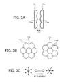
- FIGS. 3A to 3C are diagrams showing a concrete configuration of the microlens array units 11a and 11b according to the embodiment.
- FIG. 3A shows a cross-sectional view of the microlens array units 11a and 11b which are cut by a plane normal to a traveling direction of the light. Concretely, the cross-sectional view shows parts of the microlens array units 11a and 11b in an enlarged manner.
- the microlens array units 11a and 11b are arranged opposite to each other so that the sides on which the plural microlenses 11aa and 11ba are formed face each other.
- the plural microlenses 11aa are formed on the side of the microlens array unit 11a which faces the microlens array unit 11b, and the plural microlenses 11ba are formed on the side of the microlens array unit 11b which faces the microlens array unit 11a.
- the microlens array units 11a and 11b are arranged opposite to each other at the position where the distance between the microlens array units 11a and 11b is a distance D.
- the microlens array units 11a and 11b are arranged opposite to each other at the position where the distance D is at least longer than a focal distance of the microlenses 11aa and 11ba.
- the microlens array units 11a and 11b are arranged at the position where the distance D is equal to or larger than 1.5 times the focal distance and equal to or smaller than 3 times the focal distance.
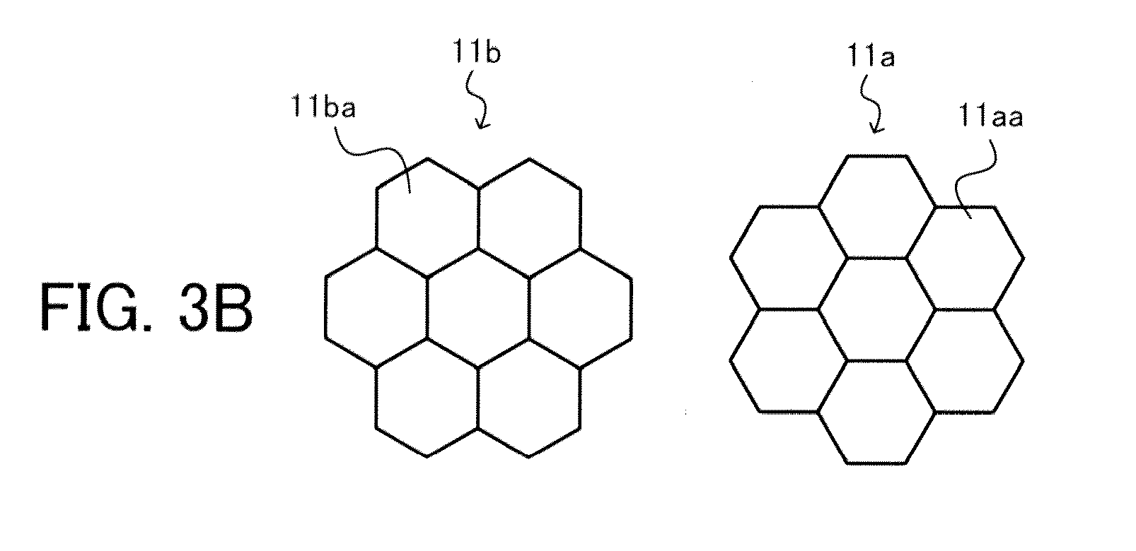
- FIG. 3B shows a plan view of the microlens array units 11a and 11b.
- the plan view shows parts of the microlens array units 11a and 11b, which are observed in the direction along the traveling direction of the light, in an enlarged manner.
- the plural microlenses 11aa and 11ba which are formed by the lens contour having the regular hexagonal shape in the plan view are arranged on the microlens array units 11a and 11b in the lattice pattern.
- the plural regular hexagonal shapes being the lens contour of the microlenses 11aa and 11ba have the same shape (namely, the same size).
- the microlenses 11aa and 11ba are formed to have the same curvature of the lens, for example.
- the direction of the vertices of the regular hexagonal shape being the lens contour of the microlenses 11aa and 11ba is defined as shown in FIG. 3C .
- the direction of the vertices is defined by a direction from a center point (center of gravity) of the regular hexagon toward each vertex of the regular hexagon.
- the right part of FIG. 3C shows the direction of the vertices of the regular hexagonal shape being the lens contour of the microlens 11aa
- the left part of FIG. 3C shows the direction of the vertices of the regular hexagonal shape being the lens contour of the microlens 11ba.
- the plural microlenses 11aa and 11ba are arranged on the microlens array units 11a and 11b in the lattice pattern (namely, the plural microlenses 11aa and 11ba are arranged in the same direction), all of the directions of the vertices of the regular hexagonal shape in the microlens array units 11a and 11b are the same.
- the microlens array units 11a and 11b are formed so that an angle difference between the direction of the vertices of the regular hexagonal shape being the lens contour of the microlens 11aa arranged on the microlens array unit 11a and the direction of the vertices of the regular hexagonal shape being the lens contour of the microlens 11ba arranged on the microlens array unit 11b becomes a predetermined angle.
- the microlens array units 11a and 11b are formed so that the angle difference between the direction of the vertices of the regular hexagonal shape being the lens contour of the microlens 11aa and the direction of the vertices of the regular hexagonal shape being the lens contour of the microlens 11ba becomes 30 degrees.
- the plural microlenses 11aa and 11ba are arranged on the microlens array units 11a and 11b so as to satisfy such a relationship that the regular hexagonal shapes being the lens contours of the microlenses 11aa and 11ba are rotated by 30 degrees with respect to each other.
- FIG. 4A shows a light intensity distribution on a focal plane of the microlens array unit 11a (The focal plane indicates the plane which is opposed to the microlens array unit 11a and is located at the focal point of the microlens 11aa. The same will apply hereinafter).
- FIG. 4A shows the lens contours of the plural microlens 11aa arranged on the microlens array unit 11a are represented by broken lines.
- FIG. 4B shows a light intensity distribution on a plane far enough away from the focal plane of the microlens array unit 11a.
- FIG. 4C shows an image diagram when the light enters the microlens array unit 11b, in such a case that the microlens array unit 11b is arranged at the position far enough away from the focal plane of the microlens array unit 11a.
- the position is the same as the position shown in FIG. 4B .
- the lens contours of the plural microlens 11ba arranged on the microlens array unit 11b are represented by broken lines.
- the microlens array unit 11b As shown in FIGS 4B and 4C , by arranging the microlens array unit 11b at the position far enough away from the focal plane of the microlens array unit 11a, it is possible to make the light from one microlens 11aa of the microlens array unit 11a enter many microlenses 11ba of the microlens array unit 11b. Then, by collecting the light by each microlens 11ba of the microlens array unit 11b, the image is formed. Therefore, since the light can be appropriately dispersed, it becomes possible to form the uniform and even image (namely, uneven brightness is suppressed).
- the microlens array units 11a and 11b are formed so as to satisfy such a relationship that the regular hexagonal shapes being the lens contours of the microlenses 11aa and 11ba are rotated by 30 degrees with respect to each other (see FIGS. 3B and 3C ), it is possible to suppress an unnecessary interference between the image of the regular hexagonal shape on the incident side of the microlens array unit 11b due to the microlens array unit 11a and the regular hexagonal shape being the lens contour of the microlens array unit 11b.
- the direction of the vertices of the lens contour of the microlens array unit 11a is shifted from the direction of the vertices of the lens contour of the microlens array unit 11b, it is possible to blur the image of the regular hexagonal shape on the incident side of the microlens array unit 11b. Therefore, it becomes possible to appropriately suppress the influence of the shift of the position between the microlens array unit 11a and the microlens array unit 11b.
- the angle difference between the directions of the vertices being the lens contours of the microlens array units 11a and 11b is not 30 degrees, it is possible to suppress the above unnecessary interference due to the image of the regular hexagonal shape. Namely, while such an example that the angle difference between the directions of the vertices being the lens contours of the microlens array units 11a and 11b is 30 degrees is shown, the angle difference need not be exactly 30 degrees, and the angle difference may be a different angle from 30 degrees.
- the directions of the vertices of the regular hexagonal shapes being the lens contours of the microlens array units 11a and 11b are shifted to some extent (namely, the directions of the vertices of the regular hexagonal shapes do not coincide), it is possible to blur the image of the regular hexagonal shape on the incident side by the microlens array unit 11b.
- the effect of suppression of the unnecessary interference due to the image of the regular hexagonal shape increases when the angle difference between the directions of the vertices of the regular hexagonal shapes being the lens contours is 30 degrees or 90 degrees. Therefore, it is preferred that the angle difference between the directions of the vertices of the regular hexagonal shapes being the lens contours of the microlens array units 11a and 11b is substantially 30 degrees or substantially 90 degrees.
- the screen (hereinafter referred to as "screen according to comparative example") formed by the two microlens arrays.
- the two microlens arrays are spaced at the focal distance of the microlens, and the two microlens arrays are arranged so that the directions of the vertices of the hexagonal shapes or the tetragonal shapes being the lens contours of the microlens coincide (namely, the angle difference between the directions of the vertices becomes 0).
- the configuration of the comparative example it is necessary to exactly adjust the position of the two microlens arrays.
- the microlens array units 11a and 11b are arranged at the position where the distance between the microlens array units 11a and 11b is at least longer than the focal distance of the microlenses 11aa and 11ba.
- the resolution tends to decrease, it is possible to reduce the accuracy necessary to arrange the microlens array units 11a and 11b opposite to each other.
- the microlens array units 11a and 11b are arranged so that the directions of the vertices of the lens contours of the microlens array units 11a and 11b are shifted by the predetermined angle.
- the directions of the vertices of the lens contours of the microlens array units 11a and 11b it is not necessary that the directions of the vertices of the lens contours of the microlens array units 11a and 11b exactly coincide and the angle difference between the directions of the vertices of the lens contours is exactly set to the predetermined angle.
- the embodiment it is possible to appropriately cope with the light, the field angle of which is relatively large. Therefore, it is not necessary to use the condenser lens in the Patent Reference-1, which is located between the laser projector and the microlens array. So, according to the embodiment, it is possible to reduce the number of components in the image display device 1.
- the microlens array units 11a and 11b on which the microlenses 11aa and 11ba are arranged are produced, in such a state that the regular hexagonal shapes being the lens contours of the microlenses 11aa and 11ba are rotated by 15 degrees being half of 30 degrees, as shown in FIG. 5 .
- an axis AX1 is defined as a horizontal axis of the microlens array units 11a and 11b
- an axis AX2 is defined as a horizontal axis of the microlenses 11aa and 11ba
- an axis AX3 is defined as a vertical axis of the microlenses 11aa and 11ba
- the microlens array units 11a and 11b on which the plural microlenses 11aa and 11ba are arranged are produced so that the horizontal axis AX2 of the microlenses 11aa and 11ba is inclined with respect to the horizontal axis AX1 of the microlens array units 11a and 11b by 15 degrees.
- the same microlens array units 11a and 11b are produced. Namely, in the embodiment, two microlens array units on which the plural microlenses 11aa and 11ba are similarly arranged as shown in FIG. 5 are produced, and the two microlens array units are used as the microlens array units 11a and 11b.
- the microlens array units 11a and 11b produced by the above manner are arranged so that the sides on which the plural microlenses 11aa and 11ba are formed face each other and the microlens array units 11a and 11b are positioned opposite to each other at the position where the distance between the microlens array units 11a and 11b is the predetermined distance D (see FIG. 3A ).
- the microlens array units 11a and 11b are positioned opposite to each other so that the directions of the horizontal axes AX1 of the microlens arrayunits 11a and 11b coincide.
- the angle difference between the direction of the vertices of the regular hexagonal shape being the lens contour of the microlens 11aa arranged on the microlens array unit 11a and the direction of the vertices of the regular hexagonal shape being the lens contour of the microlens 11ba arranged on the microlens array unit 11b becomes 30 degrees. Namely, such a relationship that the regular hexagonal shapes being the lens contours of the microlenses 11aa and 11ba are rotated by 30 degrees with respect to each other is satisfied.
- microlens array units 11a and 11b are formed into a substantially circular shape (namely, a substantially discoid shape), it is not necessary to produce the microlens array units 11a and 11b on which the microlenses 11aa and 11ba are arranged in such a state that the regular hexagonal shapes being the lens contours are rotated by the 15 degrees.
- the same microlens array units 11a and 11b on which the microlenses 11aa and 11ba are arranged in such a state that the regular hexagonal shapes being the lens contours are not rotated may be produced, and the microlens array units 11a and 11b may be arranged opposite to each other so that the regular hexagonal shapes being the lens contours are rotated by 30 degrees with respect to each other.
- the plural microlenses 11aa are formed on the side of the microlens array unit 11a which faces the microlens array unit 11b and the plural microlenses 11ba are formed on the side of the microlens array unit 11b which faces the microlens array unit 11a.
- plural microlenses of one of two microlens array units are formed on a side which faces the other, and plural microlenses of the other are formed on a side which does not face the one.
- FIGS. 6A and 6B are diagrams showing a concrete configuration of a screen 111 according to the first modification.
- FIG. 6A shows a cross-sectional view of microlens array units 111a and 111b in the screen 111, which are cut by the plane normal to the traveling direction of the light. Concretely, the cross-sectional view shows parts of the microlens array units 111a and 111b in an enlarged manner. As shown in FIG.
- plural microlenses 111aa are formed on a side of the microlens array unit 111a which does not face the microlens array unit 111b
- plural microlenses 111ba are formed on a side of the microlens array unit 111b which faces the microlens array unit 111a.
- the microlens array units 111a and 111b are positioned opposite to each other so that the side of the microlens array unit 111a on which the plural microlenses 111aa are not formed and the side of the microlens array unit 111b on which the plural microlenses 111ba are formed face each other.
- microlens array units 111a and 111b are arranged opposite to each other at the position where the distance between the microlens array units 111a and 111b is a distance D1 which is at least longer than the focal distance of the microlenses 111aa and 111ba.
- FIG. 6B shows a plan view of the microlens array units 111a and 111b.
- the plan view shows parts of the microlens array units 111a and 111b, which are observed in the direction along the traveling direction of the light, in an enlarged manner.
- the plural microlenses 111aa and 111ba which are formed by the lens contour having the regular hexagonal shape in the plan view are arranged on the microlens array units 111a and 111b in the lattice pattern.
- microlens array units 111a and 111b are formed so that the angle difference between the direction of the vertices of the regular hexagonal shape being the lens contour of the microlens 111aa arranged on the microlens array unit 111a and the direction of the vertices of the regular hexagonal shape being the lens contour of the microlens 111ba arranged on the microlens array unit 111b becomes 30 degrees.
- a second modification is different from the embodiment and the first modification in that plural microlenses of one of two microlens array units are formed on a side which does not face the other, and plural microlenses of the other are formed on a side which does not face the one.
- FIGS. 7A and 7B are diagrams showing a concrete configuration of a screen 112 according to the secondmodification.
- FIG. 7A shows a cross-sectional view of microlens array units 112a and 112b in the screen 112, which are cut by the plane normal to the traveling direction of the light. Concretely, the cross-sectional view shows parts of the microlens array units 112a and 112b in an enlarged manner. As shown in FIG.
- plural microlenses 112aa are formed on a side of the microlens array unit 112a which does not face the microlens array unit 112b
- plural microlenses 112ba are formed on a side of the microlens array unit 112b which does not face the microlens array unit 112a.
- the microlens array units 112a and 112b are positioned opposite to each other so that the sides of the microlens array units 112a and 112b on which the plural microlenses 112aa and 112ba are formed do not face each other.
- microlens array units 112a and 112b are arranged opposite to each other at the position where the distance between the microlens array units 112a and 112b is a distance D2 which is at least longer than the focal distance of the microlenses 112aa and 112ba.
- FIG. 7B shows a plan view of the microlens array units 112a and 112b.
- the plan view shows parts of the microlens array units 112a and 112b, which are observed in the direction along the traveling direction of the light, in an enlarged manner.
- the plural microlenses 112aa and 112ba which are formed by the lens contour having the regular hexagonal shape in the plan view are arranged on the microlens array units 112a and 112b in the lattice pattern.
- microlens array units 112a and 112b are formed so that the angle difference between the direction of the vertices of the regular hexagonal shape being the lens contour of the microlens 112aa arranged on the microlens array unit 112a and the direction of the vertices of the regular hexagonal shape being the lens contour of the microlens 112ba arranged on the microlens array unit 112b becomes 30 degrees.
- the two microlens array units are separated. Meanwhile, in a third modification, two microlens array units are integrated, and plural microlenses are formed on both sides of a screen.
- FIGS. 8A and 8B are diagrams showing a concrete configuration of a screen 113 according to the third modification.
- FIG. 8A shows a cross-sectional view of the screen 113 which are cut by the plane normal to the traveling direction of the light. Concretely, the cross-sectional view shows parts of the screen 113 in an enlarged manner.
- plural microlenses 113aa and 113ba are formed on two sides (namely, both sides) of the screen 113 which are opposed to each other.
- the microlens array unit 113a on which the plural microlenses 113aa are formed is integrated with the microlens array unit 113b on which the plural microlenses 113ba are formed.
- the opposite side of the side on which the plural microlenses 113aa of the microlens array unit 113a are formed abuts the opposite side of the side on which the plural microlenses 113ba of the microlens array unit 113b are formed, so as to integrate the microlens array unit 113a with the microlens array unit 113b.
- the plural microlenses 113aa and the plural microlenses 113ba are arranged at the position where the distance between the microlenses 113aa and 113ba is a distance D3 which is at least longer than the focal distance.
- the screen 13 has a thickness corresponding to the distance D3 which is at least longer than the focal distance of the microlenses 113aa and 113ba.
- FIG. 8B shows a plan view of the microlens array units 113a and 113b.
- the plan view shows parts of the microlens array units 113a and 113b, which are observed in the direction along the traveling direction of the light, in an enlarged manner.
- the plural microlenses 113aa and 113ba which are formed by the lens contour having the regular hexagonal shape in the plan view are arranged on the microlens array units 113a and 113b in the lattice pattern.
- microlens array units 113a and 113b are formed so that the angle difference between the direction of the vertices of the regular hexagonal shape being the lens contour of the microlens 113aa arranged on the microlens array unit 113a and the direction of the vertices of the regular hexagonal shape being the lens contour of the microlens 113ba arranged on the microlens array unit 113b becomes 30 degrees.
- the third modification since the two microlens array units 113a and 113b in the screen 113 are integrated, it is only necessary to produce one component on which the microlens arrays are formed. Therefore, compared with the embodiment and the first and second modifications, it becomes possible to further reduce the cost necessary for the screen 113.
- the screens according to the embodiment and the first to third modifications are formed by the microlens array unit comprising the microlenses, the lens contour of which has the regular hexagonal shape. Meanwhile, a screen according to a fourth modification is formed by a microlens array unit comprising microlenses, a lens contour of which has a square shape.
- FIG. 9 is a diagram showing a concrete configuration of a screen 114 according to the fourth modification.
- FIG. 9 shows a plan view showing the microlens array units 114a and 114b in the screen 114, which are observed in the direction along the traveling direction of the light, in an enlarged manner.
- plural microlenses 114aa and 114ba which are formed by the lens contour having the square shape in the plan view are arranged on the microlens array units 114a and 114b in the lattice pattern.
- the microlens array units 114a and 114b are formed so that the angle difference between the direction of the vertices of the square shape being the lens contour of the microlens 114aa arranged on the microlens array unit 114a and the direction of the vertices of the square shape being the lens contour of the microlens 114ba arranged on the microlens array unit 114b becomes 45 degrees.
- the plural microlenses 114aa and 114ba are arranged on the microlens array units 114a and 114b so as to satisfy such a relationship that the square shapes being the lens contours of the microlenses 114aa and 114ba are rotated by 45 degrees with respect to each other.
- microlens array units 114a and 114b are arranged opposite to each other at the position where the distance between the microlens array units 114a and 114b is at least longer than the focal distance of the microlenses 114aa and 114ba.
- one of the arrangements in the embodiment and the first and second modifications is applied to the microlens array units 114a and 114b, or the microlens array units 114a and 114b are integrated as shown in the third modification.
- microlenses 114aa and 114ba having the square shape is arranged as shown in FIG. 9 .
- the microlenses 114aa and 114ba are arranged on the microlens array units 114a and 114b so that the positions of the adjoiningmicrolenses 114aa and 114ba in a vertical direction (corresponding to the direction of the axis AX3 in FIG. 5 . The same will apply hereinafter) coincide.
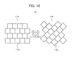
- microlenses can be arranged as shown in FIG. 10 .
- FIG. 10 is a diagram showing a concrete configuration of a screen 115 according to another example of the fourth modification.
- FIG. 10 shows a plan view showing parts of microlens array units 115a and 115b in the screen 115, which are observed in the direction along the traveling direction of the light, in an enlarged manner.
- plural microlenses 115aa and 115ba which are formed by the lens contour having the square shape in the plan view are arranged on the microlens array units 115a and 115b.
- the microlenses 115aa and 115ba are arranged on the microlens array units 115a and 115b so that the positions of the adjoining microlenses 115aa and 115ba in the vertical direction are shifted by half of a length of one side of the square shape. Additionally, the microlens array units 115a and 115b are formed so that the angle difference between the direction of the vertices of the square shape being the lens contour of the microlens 115aa arranged on the microlens array unit 115a and the direction of the vertices of the square shape being the lens contour of the microlens 115ba arranged on the microlens array unit 115b becomes 45 degrees.
- the screen 115 it is possible to achieve the same effect as the above screen 114, too.
- the angle difference between the directions of the vertices of the square shapes being the lens contours of the microlens array units 114a, 114b, 115a and 115b is 45 degrees
- the angle difference need not be exactly 45 degrees, and the angle difference may be a different angle from 45 degrees.
- the reason is as described in the section "[Operation and Effect of Screen]" in the embodiment.
- the angle difference between the directions of the vertices of the square shapes being the lens contours is 45 degrees or 135 degrees. Therefore, it is preferred that the angle difference between the directions of the vertices of the square shapes being the lens contours of the microlens array units 114a, 114b, 115a and 115b is substantially 45 degrees or substantially 135 degrees.
- the screens according to the embodiment and the first to fourth modifications are formed by the microlens array unit comprising the microlenses, the lens contour of which has the regular hexagonal shape or the square shape. Meanwhile, a screen according to a fifth modification is formed by a microlens array unit comprising microlenses, a lens contour of which has a circular shape.
- FIG. 11 is a diagram showing a concrete configuration of a screen 116 according to the fifth modification.
- FIG. 11 shows a plan view showing parts of the microlens array units 116a and 116b in the screen 116, which are observed in the direction along the traveling direction of the light, in an enlarged manner.
- plural microlenses 116aa and 116ba which are formed by the lens contour having the circular shape in the plan view are arranged on the microlens array units 116a and 116b.
- the microlenses 116aa and 116ba are arranged around one microlens, and are adjacently arranged at each predetermined angle with respect to vertices of the one microlens.
- FIG. 11 shows such an example that the predetermined angle is 60 degrees.
- the microlenses 116aa arranged on the microlens array unit 116a and the microlens 116ba arranged on the microlens array unit 116b are shifted by 30 degrees, corresponding to half of the predetermined angle, with respect to the one microlens.
- microlens array units 116a and 116b are arranged opposite to each other at the position where the distance between the microlens array units 116a and 116b is at least longer than the focal distance of the microlenses 116aa and 116ba.
- one of the arrangements in the embodiment and the first and second modifications is applied to the microlens array units 116a and 116b, or the microlens array units 116a and 116b are integrated as shown in the third modification.
- a space between the microlenses 116aa and 116ba formed on the microlens array units 116a and 116b is masked so that the light does not go through the space.
- the screens according to the embodiment and the first to fourth modifications are formed by the microlens array unit comprising the microlenses, the lens contour of which has the regular polygonal shape (regular hexagonal shape or square shape) in which lengths of all sides are the same.
- a screen according to a sixth modification is formed by a microlens array unit comprising microlenses, a lens contour of which has a polygonal shape not being the regular polygonal shape (namely, lengths of all sides in the polygonal shape are not the same).
- FIGS. 12A and 12B are diagrams showing a concrete configuration of a screen 117 according to the sixth modification.
- FIG. 12A shows a plan view showing parts of microlens array units 117a and 117b in the screen 117, which are observed in the direction along the traveling direction of the light, in an enlarged manner.
- plural microlenses 117aa and 117ba which are formed by the lens contour having a hexagonal shape in the plan view are arranged on the microlens array units 117a and 117b in the lattice pattern.
- the microlenses 117aa and 117ba are formed by the hexagonal-shaped lens contour having a line-symmetric shape, not being the regular hexagonal shape (namely, lengths of all sides are not the same).
- FIG. 12B shows directions of vertices of the lens contours of the microlenses 117aa and 117ba.
- the microlens array units 117a and 117b are formed so that the angle difference between the direction of the vertices of the hexagonal shape being the lens contour of the microlens 117aa arranged on the microlens array unit 117a and the direction of the vertices of the hexagonal shape being the lens contour of the microlens 117ba arranged on the microlens array unit 117b becomes 90 degrees.
- the plural microlenses 117aa and 117ba are arranged on the microlens array units 117a and 117b so as to satisfy such a relationship that the hexagonal shapes being the lens contours of the microlenses 117aa and 117ba are rotated by 90 degrees with respect to each other.
- microlens array units 117a and 117b are arranged opposite to each other at the position where the distance between the microlens array units 117a and 117b is at least longer than the focal distance of the microlenses 117aa and 117ba.
- one of the arrangements in the embodiment and the first and second modifications is applied to the microlens array units 117a and 117b, or the microlens array units 117a and 117b are integrated as shown in the third modification.
- the hexagonal shape as shown in FIG. 12A is one example of the polygonal shape. It is not limited that the lens contour of the microlens is formed by the hexagonal shape. Additionally, it is not limited that the angle difference between the directions of the vertices of the hexagonal shapes being the lens contours is 90 degrees as shown in FIG. 12B .
- the present invention is applied to the head-up display, it is not limited to this.
- the present invention can be applied to a laser projector. Since a speckle noise normally poses a problem for the laser projector, it is not preferred that a screen for a liquid crystal projector is applied to the laser projector. However, since the screen in the present invention can appropriately suppress the speckle noise and can sufficiently ensure a view angle, the screen in the present invention can be preferably applied to the laser projector.
- This invention can be used for image display devices such as a head-up display and a laser projector.
Landscapes
- Physics & Mathematics (AREA)
- General Physics & Mathematics (AREA)
- Optics & Photonics (AREA)
- Liquid Crystal (AREA)
- Devices For Indicating Variable Information By Combining Individual Elements (AREA)
Abstract

Description
- The present invention relates to an optical element using a microlens array.
- Conventionally, there is proposed a technique for applying a transmissive screen using a microlens array to a head-up display and a laser projector. When the transmissive screen is used, there is an advantage that it is possible to suppress an influence of a speckle noise compared with a case of using a diffuser. For example, in Patent Reference-1, there is proposed an image forming device including a light source of a laser, a laser projector which projects an image formed by an array of plural pixels, and a microlens array on which plural microlenses are arranged. When the microlens array is used, it is possible to appropriately disperse an incident light and freely design a necessary diffusing angle.
- Meanwhile, in
Patent References 2 and 3 andNon-Patent Reference 1, there is proposed a screen formed by two microlens arrays or two diffraction gratings, for example. Specifically, Non-PatentReference 1 discloses that though an uneven brightness tends to occur when only one microlens array is used, the uneven brightness can be suppressed by using two microlens arrays. -
- Patent Reference-1: Japanese Patent Application Laid-open under No.
2010-145745 - Patent Reference-2: Japanese Patent Application Laid-open under No.
08-16656 - Patent Reference-3 : Japanese Patent Application Laid-open under No.
2007-523369 - Non-Patent Reference 1: H. Urey and K. D. Powell, "Microlens-array-based exit-pupil expander for full-color displays", APPLIED OPTICS Vol.44, No.23, p.4930-4936
- Basically, as for the above conventional techniques using the screen formed by the two microlens arrays (including the screen formed by the two diffraction gratings. The same will apply hereinafter), the two microlens arrays are spaced at a focal distance of the microlens, and the two microlens arrays are arranged so that a direction of vertices of a hexagonal shape or a tetragonal shape being a lens contour of the microlens coincides. By the above configuration of the conventional techniques, it is necessary to exactly adjust the position of the two microlens arrays. This is because, if the distance between the two microlens arrays does not coincide with the focal distance or the direction of the vertices of the lens contour of the microlens does not coincide, there sometimes occurs such a problem that the microlens takes in an unnecessary light or an influence of the inconsistency is perceived. Therefore, by the conventional techniques, there is a tendency that the time and cost of producing the screen increase.
- The present invention has been achieved in order to solve the above problem. It is an object of the present invention to provide an optical element, a head-up display and a method for producing an optical element which can suppress an influence of a shift of a position between microlens arrays and can easily be produced.
- In the invention according to
claim 1, an optical element includes a first microlens array unit and a second microlens array unit on which plural microlenses are arranged, wherein the plural microlenses are formed by a lens contour having a polygonal shape in a plan view, and wherein the first and second microlens array units are arranged opposite to each other at a position where a distance between the first and second microlens array units is at least longer than a focal distance of the microlens, and are formed so that a direction of vertices of the lens contour of the microlens arranged on the first microlens array unit is different from a direction of vertices of the lens contour of the microlens arranged on the second microlens array unit. - In the invention according to
claim 11, a head-up display includes the optical element according toclaim 1 and makes a user perceive an image formed by the optical element as a virtual image at an eye position of the user. - In the invention according to claim 12, a method for producing an optical element including a first microlens array unit and a second microlens array unit on which plural microlenses are arranged, includes: a first process which forms the plural microlenses on one side, which are arranged in such a state that a polygonal shape being a lens contour of the microlens is rotated by half of a predetermined degrees, so as to produce the first and second microlens array units; and a secondprocess which arranges the first and second microlens array units produced in the first process so that the first and second microlens array units are positioned opposite to each other at a position where a distance between the first and second microlens array units is at least longer than a focal distance of the microlens, so as to produce the optical element.
- In the invention according to claim 13, a method for producing an optical element including a first microlens array unit and a second microlens array unit on which plural microlenses are arranged, includes: a first process which forms the plural microlenses on one side so as to produce the first and second microlens array units; and a second process which arranges the first and second microlens array units opposite to each other at a position where a distance between the first and second microlens array units is at least longer than a focal distance of the microlens, and arranges the first and second microlens array units so that an angle difference between a direction of vertices of a polygonal shape being a lens contour of the microlens formed on the first microlens array unit and a direction of vertices of a polygonal shape being a lens contour of the microlens formed on the second microlens array unit becomes a predetermined angle, so as to produce the optical element.
- In the invention according to claim 14, an optical element includes a first microlens array unit and a second microlens array unit on which plural microlenses are arranged, wherein the plural microlenses are formed by a lens contour having a regular polygonal shape in a plan view, and wherein the first and second microlens array units are arranged opposite to each other at a position where a distance between the first and second microlens array units is at least longer than a focal distance of the microlens, and are formed so that an angle difference between a direction of vertices of the lens contour of the microlens arranged on the first microlens array unit and a direction of vertices of the lens contour of the microlens arranged on the second microlens array unit becomes half of an internal angle of the regular polygonal shape.
- In the invention according to
claim 15, an optical element includes a first microlens array unit and a second microlens array unit on which plural microlenses are arranged at equal distances, wherein the microlenses are arranged around one microlens and are adjacently arranged at each predetermined angle with respect to vertices of the one microlens, wherein the first and second microlens array units are arranged opposite to each other at a position where a distance between the first and second microlens array units is at least longer than a focal distance of the microlens, and wherein the microlens arranged on the first microlens array unit and the microlens arranged on the second microlens array unit are shifted by half of the predetermined angle with respect to the one microlens. -
-
FIG. 1 shows a configuration of an image display device according to an embodiment. -
FIG. 2 shows a perspective view of a screen according to an embodiment. -
FIGS. 3A to 3C show configurations of microlens array units according to an embodiment. -
FIGS. 4A to 4C show diagrams for explaining an operation and an effect of a screen according to an embodiment. -
FIG. 5 shows a diagram for explaining a method for producing a screen according to an embodiment. -
FIGS. 6A and 6B show configurations of a screen according to a first modification. -
FIGS. 7A and 7B show configurations of a screen according to a second modification. -
FIGS. 8A and 8B show configurations of a screen according to a third modification. -
FIG. 9 shows a configuration of a screen according to a fourth modification. -
FIG. 10 shows a configuration of a screen according to another example of a fourth modification. -
FIG. 11 shows a concrete configuration of a screen according to a fifth modification. -
FIGS. 12A and 12B show concrete configurations of a screen according to a sixth modification. - According to one aspect of the present invention, there is provided an optical element, including a first microlens array unit and a second microlens array unit on which plural microlenses are arranged, wherein the plural microlenses are formed by a lens contour having a polygonal shape in a plan view, and wherein the first and second microlens array units are arranged opposite to each other at a position where a distance between the first and second microlens array units is at least longer than a focal distance of the microlens, and are formed so that a direction of vertices of the lens contour of the microlens arranged on the first microlens array unit is different from a direction of vertices of the lens contour of the microlens arranged on the second microlens array unit.
- The above optical element includes the first and second microlens array units on which the plural microlenses are arranged. In other words, the optical element corresponds to a screen. The plural microlenses are formed by the lens contour having the polygonal shape in the plan view. The lens contour indicates a contour (outline) of one microlens which is formed on the first and second microlens array units. The same will apply hereinafter. The first and second microlens array units are arranged opposite to each other at the position where the distance between the first and second microlens array units is at least longer than the focal distance of the microlens. Additionally, the first and second microlens array units are formed so that the angle difference between the direction of the vertices of the polygonal shape being the lens contour of the microlens arranged on the first microlens array unit and the direction of the vertices of the polygonal shape being the lens contour of the microlens arranged on the second microlens array unit becomes a predetermined angle. Namely, the plural microlens are arranged on the first and second microlens array units so as to satisfy such a relationship that the polygonal shapes being the lens contours are rotated by the predetermined angle with each other.
- According to the above optical element, by using the first and second microlens array units which are arranged opposite to each other at the position where the distance between the first and second microlens array units is at least longer than the focal distance of the microlens, it is possible to appropriately disperse the light, and it is possible to form the uniform and even image. Additionally, since the direction of the vertices of the lens contour of the first microlens array units is different from the direction of the vertices of the lens contour of on the second microlens array unit, it is possible to suppress the unnecessary interference on the incident side due to the image of the polygonal shape, and it becomes possible to appropriately suppress the influence of the shift of the position between the first and second microlens array units. Additionally, according to the above optical element, since it is not necessary to exactly adjust the position of the first and second microlens array units, it becomes possible to produce the optical element with ease and at low cost.
- In a preferred example of the above optical element, the microlenses of the first and second microlens array units are formed by the lens contour having the polygonal shape, and are arranged so that sides of the polygonal shape are adjacent to each other.
- In a preferred example of the above optical element, the first and second microlens array units are arranged opposite to each other at a position where the distance between the first and second microlens array units is equal to or larger than 1.5 times the focal distance and equal to or smaller than 3 times the focal distance.
- In a manner of the above optical element, the polygonal shape is a regular hexagonal shape, and an angle difference between the direction of the vertices of the lens contour of the microlens arranged on the first microlens array unit and the direction of the vertices of the lens contour of the microlens arranged on the second microlens array unit is substantially 30 degrees or substantially 90 degrees. Therefore, it becomes possible to effectively suppress the influence of the shift of the position between the first and second microlens array units.
- In another manner of the above optical element, the polygonal shape is a square shape, and an angle difference between the direction of the vertices of the lens contour of the microlens arranged on the first microlens array unit and the direction of the vertices of the lens contour of the microlens arranged on the second microlens array unit is substantially 45 degrees or substantially 135 degrees. Therefore, it becomes possible to effectively suppress the influence of the shift of the position between the first and second microlens array units.
- In another manner of the above optical element, the optical element further comprises a first lens array and a second lens array. The first lens array has the first microlens array unit on one side, and the second lens array has the second microlens array unit on one side. In other words, the first and second microlens array units are separated, and the plural microlenses are formed on one side of the first and second microlens array units.
- In a preferred example of the above optical element, the first microlens array unit is formed on a side of the first lens array which faces the second lens array, and the second microlens array unit is formed on a side of the second lens array which faces the first lens array. In other words, the plural microlenses are formed on the sides of the first and second microlens array units, which face each other.
- In a preferred example of the above optical element, the first microlens array unit is formed on a side of the first lens array which does not face a side of the second lens array on which the second microlens array unit is formed. In other words, the plural misrolenses of one of the first and second microlens array units are formed on the side which faces the other, and the plural misrolenses of the other are formed on the side which does not face the one.
- In a preferred example of the above optical element, the first microlens array unit is formed on a side of the first lens array which does not face the second lens array, and the second microlens array unit is formed on a side of the second lens array which does not face the first lens array. In other words, the plural microlenses are formed on the sides of the first and second microlens array units, which do not face each other.
- In another manner of the above optical element, the first microlens array unit is formed on one side of the optical element, and the second microlens array unit is formed on the other side of the optical element. In other words, the first and second microlens array units are integrated, and the plural microlenses are formed on both sides of the optical element. According to the manner, since the two microlens array units are integrated, it is only necessary to produce one component on which the microlens arrays are formed. Therefore, it becomes possible to reduce the cost necessary for the optical element more effectively.
- The above optical element can be preferably applied to a head-up display which makes a user perceive an image as a virtual image at an eye position of the user.
- According to another aspect of the present invention, there is provided a method for producing an optical element including a first microlens array unit and a second microlens array unit on which plural microlenses are arranged, including: a first process which forms the plural microlenses on one side, which are arranged in such a state that a polygonal shape being a lens contour of the microlens is rotated by half of a predetermined degrees, so as to produce the first and second microlens array units; and a second process which arranges the first and second microlens array units produced in the first process so that the first and second microlens array units are positioned opposite to each other at a position where a distance between the first and second microlens array units is at least longer than a focal distance of the microlens, so as to produce the optical element.
- According to still another aspect of the present invention, there is provided a method for producing an optical element including a first microlens array unit and a second microlens array unit on which plural microlenses are arranged, including: a first process which forms the plural microlenses on one side so as to produce the first and second microlens array units; and a second process which arranges the first and second microlens array units opposite to each other at a position where a distance between the first and second microlens array units is at least longer than a focal distance of the microlens, and arranges the first and second microlens array units so that an angle difference between a direction of vertices of a polygonal shape being a lens contour of the microlens formed on the first microlens array unit and a direction of vertices of a polygonal shape being a lens contour of the microlens formed on the second microlens array unit becomes a predetermined angle, so as to produce the optical element.
- According to the above method for producing the optical element, it becomes possible to produce the optical element with ease and at low cost.
- According to still another aspect of the present invention, there is provided an optical element, including a first microlens array unit and a second microlens array unit on which plural microlenses are arranged, wherein the plural microlenses are formed by a lens contour having a regular polygonal shape in a plan view, and wherein the first and second microlens array units are arranged opposite to each other at a position where a distance between the first and second microlens array units is at least longer than a focal distance of the microlens, and are formed so that an angle difference between a direction of vertices of the lens contour of the microlens arranged on the first microlens array unit and a direction of vertices of the lens contour of the microlens arranged on the second microlens array unit becomes half of an internal angle of the regular polygonal shape.
- According to still another aspect of the present invention, there is provided an optical element, including a first microlens array unit and a second microlens array unit on which plural microlenses are arranged at equal distances, wherein the microlenses are arranged around one microlens and are adjacently arranged at each predetermined angle with respect to vertices of the one microlens, wherein the first and second microlens array units are arranged opposite to each other at a position where a distance between the first and second microlens array units is at least longer than a focal distance of the microlens, and wherein the microlens arranged on the first microlens array unit and the microlens arranged on the second microlens array unit are shifted by half of the predetermined angle with respect to the one microlens.
- Preferably, a space between the microlenses formed on the first and second microlens array units is masked so that a light does not go through the space.
- A preferred embodiment of the present invention will be explained hereinafter with reference to the drawings.
-
FIG. 1 shows a configuration of an image display device to which the optical element in the embodiment is applied. As shown inFIG. 1 , theimage display device 1 includes an image signal input unit 2, avideo ASIC 3, aframe memory 4, aROM 5, a RAM 6, a laser driver ASIC 7, aMEMS control unit 8, a laserlight source unit 9, aMEMS mirror 10 and ascreen 11. - The
image display device 1 is applied to a head-up display, for example. The head-up display makes a driver perceive an image as a virtual image at an eye position (eye point) of the driver. - The image signal input unit 2 receives the image signal from the outside and outputs the image signal to
video ASIC 3. - The
video ASIC 3 is formed as an ASIC (Application Specific Integrated Circuit) and controls the laser driver ASIC 7 and theMEMS control unit 8 based on the image signal inputted by the image signal input unit 2 and a scanning position information Sc inputted by theMEMS mirror 10. Thevideo ASIC 3 includes a sync/image separator 31, abit data converter 32, a lightemission pattern converter 33 and atiming controller 34. - The sync/
image separator 31 separates the image signal inputted by the image signal input unit 2 into a synchronous signal and image data displayed on a screen as an image displaying unit, and writes the image data into theframe memory 4. - The
bit data converter 32 reads out the image data written into theframe memory 4, and converts the image data into bit data. - The light
emission pattern converter 33 converts the bit data converted by thebit data converter 32 into a signal indicating a light emission pattern of each laser. - The
timing controller 34 controls an operation timing of the sync/image separator 31 and thebit data converter 32. Additionally, thetiming controller 34 also controls an operation timing of theMEMS control unit 8, described later. - The image data separated by the sync/
image separator 31 is written into theframe memory 4. TheROM 5 stores a control program and data for operating thevideo ASIC 3. The RAM 6 is used as a working memory when thevideo ASIC 3 operates, and thevideo ASIC 3 sequentially reads and writes various data of the RAM 6. - The laser driver ASIC 7 is formed as an ASIC and generates a signal for driving laser diodes provided in the laser
light source unit 9 which will be described later. The laser driver ASIC 7 includes a redlaser driver circuit 71, a bluelaser driver circuit 72 and a greenlaser driver circuit 73. - The red
laser driver circuit 71 drives a red laser LD1 based on the signal outputted by the lightemission pattern converter 33. The bluelaser driver circuit 72 drives a blue laser LD2 based on the signal outputted by the lightemission pattern converter 33. The greenlaser driver circuit 73 drives a green laser LD3 based on the signal outputted by the lightemission pattern converter 33. - The
MEMS control unit 8 controls theMEMS mirror 10 based on the signal outputted by thetiming controller 34. TheMEMS control unit 8 includes aservo circuit 81 and adriver circuit 82. - The
servo circuit 81 controls the operation of theMEMS mirror 10 based on the signal from thetiming controller 34. - The
driver circuit 82 amplifies the control signal of theMEMS mirror 10, which is outputted by theservo circuit 81, to a predetermined level, and outputs the amplified signal. - The laser
light source unit 9 emits the laser light to theMEMS mirror 10 based on the drive signal outputted by the laser driver ASIC 7. - The
MEMS mirror 10 serving as a scanning unit reflects the laser light emitted by the laserlight source unit 9 to thescreen 11. Therefore, theMEMS mirror 10 forms the image to display on thescreen 11. Additionally, theMEMS mirror 10 operates to perform scanning on thescreen 11 based on the control by theMEMS control unit 8 for displaying the image inputted to the image signal input unit 2, and outputs the scanning position information (for example, an angle of the mirror 10) to thevideo ASIC 3. - The
screen 11 is an example of the optical element according to the present invention, and is formed as a transmissive screen. Thescreen 11 includes the microlens array unit (which is not shown), on which the plural microlenses are arranged. The microlens array unit moderately disperses the incident light. Concretely, the microlens array unit diffuses the light by a diffusing angle in accordance with a curvature of the lens. The curvature of the lens of the microlens array unit is preliminarily designed in accordance with a necessary diffusing angle. Thescreen 11 will be described in details, later. - Actually, the
image display device 1 makes the driver perceive the image corresponding to the light, which is outgoing from thescreen 11 and is then reflected by a reflective mirror (combiner) or is then expanded by an expander, at the eye position (eye point) of the driver. - Next, a description will be given of a concrete configuration of the laser
light source unit 9. The laserlight source unit 9 includes acase 91, a wavelengthselective element 92, acollimator lens 93, a red laser LD1, a blue laser LD2, a green laser LD3 and alight receiving element 50 for a monitor (hereinafter simply referred to as "light receiving element"). - The
case 91 has a substantially box shape and is formed by a resin. Thecase 91 is provided with aCAN fixing part 91a and acollimator fixing part 91b. TheCAN fixing part 91a is formed as a through-hole for fixing the green laser LD3 and has a concave shaped cross-section. Thecollimator fixing part 91b is formed as a through-hole provided on a plane perpendicular to theCAN fixing part 91a and has a concave shaped cross-section. - The wavelength
selective element 92 serving as a composite element is formed by a trichroic prism, for example, and is provided with a reflectingsurface 92a and a reflectingsurface 92b. The reflectingsurface 92a transmits the laser light emitted by the red laser LD1 to thecollimator lens 93, and reflects the laser light emitted by the blue laser LD2 to thecollimator lens 93. The reflectingsurface 92b transmits a large part of the laser lights emitted by the red laser LD1 and the blue laser LD2 to thecollimator lens 93, and reflects a small part of them to thelight receiving element 50. Additionally, the reflectingsurface 92b transmits a large part of the laser light emitted by the green laser LD3 to thecollimator lens 93, and reflects a small part of it to thelight receiving element 50. Thus, the emitted light from each laser is superimposed, and the superimposed light enters thecollimator lens 93 and thelight receiving element 50. The wavelengthselective element 92 is provided near thecollimator fixing part 91b in thecase 91. - The
collimator lens 93 converts the laser light from the wavelengthselective element 92 into a parallel light, and emits the parallel light to theMEMS mirror 10. Thecollimator lens 93 is fixed on thecollimator fixing part 91b in thecase 91 by an ultraviolet adhesive. Namely, thecollimator lens 93 is provided behind the composite element. - The red laser LD1 serving as the laser light source emits the red laser light. The red laser LD1 is fixed on the same axis as the wavelength
selective element 92 and thecollimator lens 93 in thecase 91, in such a state that a semiconductor laser light source remains in a chip state or the chip is placed on a submount. - The blue laser LD2 serving as the laser light source emits the blue laser light. The blue laser LD2 is fixed at the position where the emitted light can be reflected to the
collimator lens 93 by the reflectingsurface 92a, in such a state that the semiconductor laser light source remains in the chip state or the chip is placed on the submount. The position of the blue laser LD2 may be replaced with the position of the red laser LD1. - The green laser LD3 serving as the laser light source is mounted on a CAN package or a frame package, and emits the green laser light. The green laser LD3 is provided with a semiconductor laser light source chip B in the CAN package which generates the green laser light , and is fixed on the
CAN fixing part 91a in thecase 91. - The
light receiving element 50 receives a part of the laser light emitted by each laser light source. Thelight receiving element 50 is a photoelectric conversion element such as a photodetector, and supplies the laser driver ASIC 7 with a detecting signal Sd being an electrical signal in accordance with the amount of the incident laser light. Actually, thelight receiving element 50 receives one of the red laser light, the blue laser light and the green laser light in a predetermined order at the time of adjusting the power, and outputs the detecting signal Sd corresponding to the amount of the one laser light. The laser driver ASIC 7 adjusts the power of the red laser LD1, the blue laser LD2 and the green laser LD3, based on the detecting signal Sd. - For example, when the power of the red laser LD1 is adjusted, the laser driver ASIC 7 operates only the red
laser driver circuit 71 and makes the red laser LD1 emit the red laser light by supplying the driving current to the red laser LD1. Thelight receiving element 50 receives a part of the red laser light, and feeds the detecting signal Sd in accordance with the amount of the light back to the laser driver ASIC 7. The laser driver ASIC 7 adjusts the driving current which is supplied to the red laser LD1 from the redlaser driver circuit 71 so that the amount of the light corresponding to the detecting signal Sd becomes an appropriate amount of the light. Thus, the power is adjusted. Similarly, the power of the blue laser LD2 and the power of the green laser LD3 are adjusted. - Next, a concrete description will be given of a configuration of the
screen 11 according to the embodiment. -
FIG. 2 shows a perspective view of thescreen 11 according to the embodiment. As shown inFIG. 2 , thescreen 11 includes twomicrolens array units microlens array units microlens array units microlens array units -
FIGS. 3A to 3C are diagrams showing a concrete configuration of themicrolens array units FIG. 3A shows a cross-sectional view of themicrolens array units microlens array units FIG. 3A , themicrolens array units microlens array unit 11a which faces themicrolens array unit 11b, and the plural microlenses 11ba are formed on the side of themicrolens array unit 11b which faces themicrolens array unit 11a. Additionally, themicrolens array units microlens array units microlens array units microlens array units -
FIG. 3B shows a plan view of themicrolens array units microlens array units FIG. 3B , the plural microlenses 11aa and 11ba which are formed by the lens contour having the regular hexagonal shape in the plan view are arranged on themicrolens array units - Here, the direction of the vertices of the regular hexagonal shape being the lens contour of the microlenses 11aa and 11ba is defined as shown in
FIG. 3C . The direction of the vertices is defined by a direction from a center point (center of gravity) of the regular hexagon toward each vertex of the regular hexagon. The right part ofFIG. 3C shows the direction of the vertices of the regular hexagonal shape being the lens contour of the microlens 11aa, and the left part ofFIG. 3C shows the direction of the vertices of the regular hexagonal shape being the lens contour of the microlens 11ba. Since the plural microlenses 11aa and 11ba are arranged on themicrolens array units microlens array units - As shown in
FIGS. 3 and 3C , in the embodiment, themicrolens array units microlens array unit 11a and the direction of the vertices of the regular hexagonal shape being the lens contour of the microlens 11ba arranged on themicrolens array unit 11b becomes a predetermined angle. Concretely, in the embodiment, themicrolens array units microlens array units - Next, a description will be given of the operation and the effect of the
screen 11 according to the embodiment, with reference toFIGS. 4A to 4C . Hereinafter, a description will be given of an example in such a case that the light enters themicrolens array unit 11a prior to themicrolens array unit 11b, and the light emitted by themicrolens array unit 11a enters themicrolens array unit 11b. -
FIG. 4A shows a light intensity distribution on a focal plane of themicrolens array unit 11a (The focal plane indicates the plane which is opposed to themicrolens array unit 11a and is located at the focal point of the microlens 11aa. The same will apply hereinafter). InFIG. 4A , as a matter of convenience of the explanations, the lens contours of the plural microlens 11aa arranged on themicrolens array unit 11a are represented by broken lines.FIG. 4B shows a light intensity distribution on a plane far enough away from the focal plane of themicrolens array unit 11a. Concretely, the plane is opposed to themicrolens array unit 11a, and is located at the position where the distance from themicrolens array unit 11a is longer than the focal distance of the microlens 11aaFIG. 4C shows an image diagram when the light enters themicrolens array unit 11b, in such a case that themicrolens array unit 11b is arranged at the position far enough away from the focal plane of themicrolens array unit 11a. The position is the same as the position shown inFIG. 4B . InFIG. 4C , as a matter of convenience of the explanations, the lens contours of the plural microlens 11ba arranged on themicrolens array unit 11b are represented by broken lines. - As shown in
FIGS 4B and 4C , by arranging themicrolens array unit 11b at the position far enough away from the focal plane of themicrolens array unit 11a, it is possible to make the light from one microlens 11aa of themicrolens array unit 11a enter many microlenses 11ba of themicrolens array unit 11b. Then, by collecting the light by each microlens 11ba of themicrolens array unit 11b, the image is formed. Therefore, since the light can be appropriately dispersed, it becomes possible to form the uniform and even image (namely, uneven brightness is suppressed). - Here, as shown by the broken lines in
FIG. 4B , there is a case that an image of a regular hexagonal shape corresponding to the lens contour of themicrolens array unit 11a is generated on the plane far enough away from the focal plane of themicrolens array unit 11a. Namely, there is a case that the image of the regular hexagonal shape due to themicrolens array unit 11a is generated on the incident side of themicrolens array unit 11b. There is a possibility that the above image of the regular hexagonal shape is perceived. In the embodiment, since themicrolens array units FIGS. 3B and 3C ), it is possible to suppress an unnecessary interference between the image of the regular hexagonal shape on the incident side of themicrolens array unit 11b due to themicrolens array unit 11a and the regular hexagonal shape being the lens contour of themicrolens array unit 11b. Namely, According to the embodiment, since the direction of the vertices of the lens contour of themicrolens array unit 11a is shifted from the direction of the vertices of the lens contour of themicrolens array unit 11b, it is possible to blur the image of the regular hexagonal shape on the incident side of themicrolens array unit 11b. Therefore, it becomes possible to appropriately suppress the influence of the shift of the position between themicrolens array unit 11a and themicrolens array unit 11b. - Even if the angle difference between the directions of the vertices being the lens contours of the
microlens array units microlens array units microlens array units microlens array unit 11b. However, according to an experiment, it is discovered that the effect of suppression of the unnecessary interference due to the image of the regular hexagonal shape increases when the angle difference between the directions of the vertices of the regular hexagonal shapes being the lens contours is 30 degrees or 90 degrees. Therefore, it is preferred that the angle difference between the directions of the vertices of the regular hexagonal shapes being the lens contours of themicrolens array units - Meanwhile, in the above
Non-Patent Reference 1, there is proposed the screen (hereinafter referred to as "screen according to comparative example") formed by the two microlens arrays. Basically, as for the screen according to the comparative example, the two microlens arrays are spaced at the focal distance of the microlens, and the two microlens arrays are arranged so that the directions of the vertices of the hexagonal shapes or the tetragonal shapes being the lens contours of the microlens coincide (namely, the angle difference between the directions of the vertices becomes 0). By the configuration of the comparative example, it is necessary to exactly adjust the position of the two microlens arrays. This is because, if the distance between the two microlens arrays does not coincide with the focal distance or the directions of the vertices of the lens contours of the microlens do not coincide, there sometimes occurs such a problem that the microlens takes in the unnecessary light or the influence of the inconsistency is perceived. Therefore, by the comparative example, there is a tendency that the time and cost of producing the screen increase. - On the contrary, in the embodiment, the
microlens array units microlens array units microlens array units - Additionally, in the embodiment, the
microlens array units microlens array units microlens array units microlens array units screen 11 with ease and at low cost. - Additionally, according to the embodiment, it is possible to appropriately cope with the light, the field angle of which is relatively large. Therefore, it is not necessary to use the condenser lens in the Patent Reference-1, which is located between the laser projector and the microlens array. So, according to the embodiment, it is possible to reduce the number of components in the
image display device 1. - Next, a description will be given of a method for producing the
screen 11 according to the embodiment, with reference toFIG. 5 . Hereinafter, a description will be given of an example of thescreen 11 including the rectangular-shapedmicrolens array units - At first, in the embodiment, the
microlens array units FIG. 5 . Concretely, when an axis AX1 is defined as a horizontal axis of themicrolens array units microlens array units microlens array units microlens array units FIG. 5 are produced, and the two microlens array units are used as themicrolens array units - Next, the
microlens array units microlens array units microlens array units FIG. 3A ). Concretely, themicrolens array units microlens array unit 11a and the direction of the vertices of the regular hexagonal shape being the lens contour of the microlens 11ba arranged on themicrolens array unit 11b becomes 30 degrees. Namely, such a relationship that the regular hexagonal shapes being the lens contours of the microlenses 11aa and 11ba are rotated by 30 degrees with respect to each other is satisfied. - According to the above method for producing the
screen 11, since it is not necessary to produce two microlens array units which are different in the configuration and it is only necessary to produce two microlens array units which are the same in the configuration, it becomes possible to produce thescreen 11 with ease and at low cost. - When the
microlens array units microlens array units microlens array units microlens array units - Hereinafter, a description will be given of modifications of the embodiment. As for the same configuration as the embodiment, explanations thereof are suitably omitted. Additionally, as for the configuration which is not especially explained, the configuration is the same as the above-described embodiment. For example, the method for producing the screen as shown in
FIG. 5 can be suitably applied to the following modifications, too. - In the above embodiment, the plural microlenses 11aa are formed on the side of the
microlens array unit 11a which faces themicrolens array unit 11b and the plural microlenses 11ba are formed on the side of themicrolens array unit 11b which faces themicrolens array unit 11a. Meanwhile, in a first modification, plural microlenses of one of two microlens array units are formed on a side which faces the other, and plural microlenses of the other are formed on a side which does not face the one. -
FIGS. 6A and 6B are diagrams showing a concrete configuration of ascreen 111 according to the first modification.FIG. 6A shows a cross-sectional view ofmicrolens array units screen 111, which are cut by the plane normal to the traveling direction of the light. Concretely, the cross-sectional view shows parts of themicrolens array units FIG. 6A , plural microlenses 111aa are formed on a side of themicrolens array unit 111a which does not face themicrolens array unit 111b, and plural microlenses 111ba are formed on a side of themicrolens array unit 111b which faces themicrolens array unit 111a. Namely, themicrolens array units microlens array unit 111a on which the plural microlenses 111aa are not formed and the side of themicrolens array unit 111b on which the plural microlenses 111ba are formed face each other. Additionally, themicrolens array units microlens array units -
FIG. 6B shows a plan view of themicrolens array units microlens array units FIG. 6B , the plural microlenses 111aa and 111ba which are formed by the lens contour having the regular hexagonal shape in the plan view are arranged on themicrolens array units microlens array units microlens array unit 111a and the direction of the vertices of the regular hexagonal shape being the lens contour of the microlens 111ba arranged on themicrolens array unit 111b becomes 30 degrees. - By the
above screen 111 according to the first modification, it is possible to form the uniform and even image, and it is possible to appropriately suppress the influence of the shift of the position between themicrolens array units screen 111 with ease and at low cost. - A second modification is different from the embodiment and the first modification in that plural microlenses of one of two microlens array units are formed on a side which does not face the other, and plural microlenses of the other are formed on a side which does not face the one.
-
FIGS. 7A and 7B are diagrams showing a concrete configuration of ascreen 112 according to the secondmodification.FIG. 7A shows a cross-sectional view ofmicrolens array units screen 112, which are cut by the plane normal to the traveling direction of the light. Concretely, the cross-sectional view shows parts of themicrolens array units FIG. 7A , plural microlenses 112aa are formed on a side of themicrolens array unit 112a which does not face themicrolens array unit 112b, and plural microlenses 112ba are formed on a side of themicrolens array unit 112b which does not face themicrolens array unit 112a. Namely, themicrolens array units microlens array units microlens array units microlens array units -
FIG. 7B shows a plan view of themicrolens array units microlens array units FIG. 7B , the plural microlenses 112aa and 112ba which are formed by the lens contour having the regular hexagonal shape in the plan view are arranged on themicrolens array units microlens array units microlens array unit 112a and the direction of the vertices of the regular hexagonal shape being the lens contour of the microlens 112ba arranged on themicrolens array unit 112b becomes 30 degrees. - By the
above screen 112 according to the second modification, it is possible to form the uniform and even image, and it is possible to appropriately suppress the influence of the shift of the position between themicrolens array units screen 112 with ease and at low cost. - In the embodiment and the first and second modifications, the two microlens array units are separated. Meanwhile, in a third modification, two microlens array units are integrated, and plural microlenses are formed on both sides of a screen.
-
FIGS. 8A and 8B are diagrams showing a concrete configuration of ascreen 113 according to the third modification.FIG. 8A shows a cross-sectional view of thescreen 113 which are cut by the plane normal to the traveling direction of the light. Concretely, the cross-sectional view shows parts of thescreen 113 in an enlarged manner. As shown inFIG. 8A , plural microlenses 113aa and 113ba are formed on two sides (namely, both sides) of thescreen 113 which are opposed to each other. In other words, as for thescreen 113, themicrolens array unit 113a on which the plural microlenses 113aa are formed is integrated with themicrolens array unit 113b on which the plural microlenses 113ba are formed. Namely, the opposite side of the side on which the plural microlenses 113aa of themicrolens array unit 113a are formed abuts the opposite side of the side on which the plural microlenses 113ba of themicrolens array unit 113b are formed, so as to integrate themicrolens array unit 113a with themicrolens array unit 113b. - Additionally, as for the
screen 113, the plural microlenses 113aa and the plural microlenses 113ba are arranged at the position where the distance between the microlenses 113aa and 113ba is a distance D3 which is at least longer than the focal distance. Namely, the screen 13 has a thickness corresponding to the distance D3 which is at least longer than the focal distance of the microlenses 113aa and 113ba. -
FIG. 8B shows a plan view of themicrolens array units microlens array units FIG. 8B , the plural microlenses 113aa and 113ba which are formed by the lens contour having the regular hexagonal shape in the plan view are arranged on themicrolens array units microlens array units microlens array unit 113a and the direction of the vertices of the regular hexagonal shape being the lens contour of the microlens 113ba arranged on themicrolens array unit 113b becomes 30 degrees. - By the
above screen 113 according to the third modification, it is possible to form the uniform and even image, and it is possible to appropriately suppress the influence of the shift of the position between themicrolens array units screen 113 with ease and at low cost. - In addition, according to the third modification, since the two
microlens array units screen 113 are integrated, it is only necessary to produce one component on which the microlens arrays are formed. Therefore, compared with the embodiment and the first and second modifications, it becomes possible to further reduce the cost necessary for thescreen 113. - The screens according to the embodiment and the first to third modifications are formed by the microlens array unit comprising the microlenses, the lens contour of which has the regular hexagonal shape. Meanwhile, a screen according to a fourth modification is formed by a microlens array unit comprising microlenses, a lens contour of which has a square shape.
-
FIG. 9 is a diagram showing a concrete configuration of ascreen 114 according to the fourth modification. Concretely,FIG. 9 shows a plan view showing themicrolens array units screen 114, which are observed in the direction along the traveling direction of the light, in an enlarged manner. As shown inFIG. 9 , plural microlenses 114aa and 114ba which are formed by the lens contour having the square shape in the plan view are arranged on themicrolens array units - Additionally, the
microlens array units microlens array unit 114a and the direction of the vertices of the square shape being the lens contour of the microlens 114ba arranged on themicrolens array unit 114b becomes 45 degrees. Namely, the plural microlenses 114aa and 114ba are arranged on themicrolens array units - Additionally, the
microlens array units microlens array units FIG. 3A ,FIG. 6A andFIG. 7A ) in the embodiment and the first and second modifications is applied to themicrolens array units microlens array units - By the
above screen 114 according to the fourth modification, it is possible to form the uniform and even image, and it is possible to appropriately suppress the influence of the shift of the position between themicrolens array units screen 114 with ease and at low cost. - It is not limited that the microlenses 114aa and 114ba having the square shape is arranged as shown in
FIG. 9 . Concretely, it is not limited that the microlenses 114aa and 114ba are arranged on themicrolens array units FIG. 5 . The same will apply hereinafter) coincide. As another example, microlenses can be arranged as shown inFIG. 10 . -
FIG. 10 is a diagram showing a concrete configuration of ascreen 115 according to another example of the fourth modification. Concretely,FIG. 10 shows a plan view showing parts ofmicrolens array units screen 115, which are observed in the direction along the traveling direction of the light, in an enlarged manner. As shown inFIG. 10 , plural microlenses 115aa and 115ba which are formed by the lens contour having the square shape in the plan view are arranged on themicrolens array units microlens array units microlens array units microlens array unit 115a and the direction of the vertices of the square shape being the lens contour of the microlens 115ba arranged on themicrolens array unit 115b becomes 45 degrees. By thescreen 115, it is possible to achieve the same effect as theabove screen 114, too. - While such an example that the angle difference between the directions of the vertices of the square shapes being the lens contours of the
microlens array units microlens array units - The screens according to the embodiment and the first to fourth modifications are formed by the microlens array unit comprising the microlenses, the lens contour of which has the regular hexagonal shape or the square shape. Meanwhile, a screen according to a fifth modification is formed by a microlens array unit comprising microlenses, a lens contour of which has a circular shape.
-
FIG. 11 is a diagram showing a concrete configuration of ascreen 116 according to the fifth modification. Concretely,FIG. 11 shows a plan view showing parts of themicrolens array units screen 116, which are observed in the direction along the traveling direction of the light, in an enlarged manner. As shown inFIG. 11 , plural microlenses 116aa and 116ba which are formed by the lens contour having the circular shape in the plan view are arranged on themicrolens array units - Specifically, the microlenses 116aa and 116ba are arranged around one microlens, and are adjacently arranged at each predetermined angle with respect to vertices of the one microlens.
FIG. 11 shows such an example that the predetermined angle is 60 degrees. Additionally, the microlenses 116aa arranged on themicrolens array unit 116a and the microlens 116ba arranged on themicrolens array unit 116b are shifted by 30 degrees, corresponding to half of the predetermined angle, with respect to the one microlens. - Additionally, the
microlens array units microlens array units FIG. 3A ,FIG. 6A andFIG. 7A ) in the embodiment and the first and second modifications is applied to themicrolens array units microlens array units - In the fifth modification, it is preferred that a space between the microlenses 116aa and 116ba formed on the
microlens array units - By the
above screen 116 according to the fifth modification, it is possible to form the uniform and even image, and it is possible to appropriately suppress the influence of the shift of the position between themicrolens array units screen 116 with ease and at low cost. - The screens according to the embodiment and the first to fourth modifications are formed by the microlens array unit comprising the microlenses, the lens contour of which has the regular polygonal shape (regular hexagonal shape or square shape) in which lengths of all sides are the same. Meanwhile, a screen according to a sixth modification is formed by a microlens array unit comprising microlenses, a lens contour of which has a polygonal shape not being the regular polygonal shape (namely, lengths of all sides in the polygonal shape are not the same).
-
FIGS. 12A and 12B are diagrams showing a concrete configuration of ascreen 117 according to the sixth modification. Concretely,FIG. 12A shows a plan view showing parts ofmicrolens array units screen 117, which are observed in the direction along the traveling direction of the light, in an enlarged manner. As shown inFIG. 12A , plural microlenses 117aa and 117ba which are formed by the lens contour having a hexagonal shape in the plan view are arranged on themicrolens array units -
FIG. 12B shows directions of vertices of the lens contours of the microlenses 117aa and 117ba. As shown inFIG. 12B , themicrolens array units microlens array unit 117a and the direction of the vertices of the hexagonal shape being the lens contour of the microlens 117ba arranged on themicrolens array unit 117b becomes 90 degrees. Namely, the plural microlenses 117aa and 117ba are arranged on themicrolens array units - Additionally, the
microlens array units microlens array units FIG. 3A ,FIG. 6A andFIG. 7A ) in the embodiment and the first and second modifications is applied to themicrolens array units microlens array units - By the
above screen 117 according to the sixth modification, it is possible to form the uniform and even image, and it is possible to appropriately suppress the influence of the shift of the position between themicrolens array units screen 117 with ease and at low cost. - The hexagonal shape as shown in
FIG. 12A is one example of the polygonal shape. It is not limited that the lens contour of the microlens is formed by the hexagonal shape. Additionally, it is not limited that the angle difference between the directions of the vertices of the hexagonal shapes being the lens contours is 90 degrees as shown inFIG. 12B . - While the above embodiment and modifications show such an example that the present invention is applied to the head-up display, it is not limited to this. Other than the head-up display, the present invention can be applied to a laser projector. Since a speckle noise normally poses a problem for the laser projector, it is not preferred that a screen for a liquid crystal projector is applied to the laser projector. However, since the screen in the present invention can appropriately suppress the speckle noise and can sufficiently ensure a view angle, the screen in the present invention can be preferably applied to the laser projector.
- This invention can be used for image display devices such as a head-up display and a laser projector.
-
- 1
- Image Display Device
- 11
- Screen
- 11a, 11b
- Microlens Array Unit
- 11aa, 11ba
- Microlens
- 111, 112, 113, 114, 115, 116, 117
- Screen
Claims (16)
- An optical element comprising:a first microlens array unit and a second microlens array unit on which plural microlenses are arranged,wherein the pl ural microlenses are formed by a lens contour having a polygonal shape in a plan view, andwherein the first and second microlens array units are arranged opposite to each other at a position where a distance between the first and second microlens array units is at least longer than a focal distance of the microlens, and are formed so that a direction of vertices of the lens contour of the microlens arranged on the first microlens array unit is different from a direction of vertices of the lens contour of the microlens arranged on the second microlens array unit.
- The optical element according to claim 1,
wherein the microlenses of the first and second microlens array units are formed by the lens contour having the polygonal shape, and are arranged so that sides of the polygonal shape are adjacent to each other. - The optical element according to claim 1,
wherein the first and second microlens array units are arranged opposite to each other at a position where the distance between the first and second microlens array units is equal to or larger than 1.5 times the focal distance and equal to or smaller than 3 times the focal distance. - The optical element according to claim 1,
wherein the polygonal shape is a regular hexagonal shape, and
wherein an angle difference between the direction of the vertices of the lens contour of the microlens arranged on the first microlens array unit and the direction of the vertices of the lens contour of the microlens arranged on the second microlens array unit is substantially 30 degrees or substantially 90 degrees. - The optical element according to claim 1,
wherein the polygonal shape is a square shape, and
wherein an angle difference between the direction of the vertices of the lens contour of the microlens arranged on the first microlens array unit and the direction of the vertices of the lens contour of the microlens arranged on the second microlens array unit is substantially 45 degrees or substantially 135 degrees. - The optical element according to claim 1, further comprising a first lens array and a second lens array,
wherein the first lens array has the first microlens array unit on one side, and
wherein the second lens array has the second microlens array unit on one side. - The optical element according to claim 6,
wherein the first microlens array unit is formed on a side of the first lens array which faces the second lens array, and
wherein the second microlens array unit is formed on a side of the second lens array which faces to the first lens array. - The optical element according to claim 6,
wherein the first microlens array unit is formed on a side of the first lens array which does not face a side of the second lens array on which the second microlens array unit is formed. - The optical element according to claim 6,
wherein the first microlens array unit is formed on a side of the first lens array which does not face the second lens array, and
wherein the second microlens array unit is formed on a side of the second lens array which does not face the first lens array. - The optical element according to claim 1, wherein the first microlens array unit is formed on one side of the optical element, and the second microlens array unit is formed on the other side of the optical element.
- A head-up display which includes the optical element according to claim 1 and makes a user perceive an image formed by the optical element as a virtual image at an eye position of the user.
- A method for producing an optical element including a first microlens array unit and a second microlens array unit on which plural microlenses are arranged, comprising:a first process which forms the plural microlenses on one side, which are arranged in such a state that a polygonal shape being a lens contour of the microlens is rotated by half of a predetermined degrees, so as to produce the first and second microlens array units; anda second process which arranges the first and second microlens array units produced in the first process so that the first and second microlens array units are positioned opposite to each other at a position where a distance between the first and second microlens array units is at least longer than a focal distance of the microlens, so as to produce the optical element.
- A method for producing an optical element including a first microlens array unit and a second microlens array unit on which plural microlenses are arranged, comprising:a first process which forms the plural microlenses on one side so as to produce the first and second microlens array units; anda second process which arranges the first and second microlens array units opposite to each other at a position where a distance between the first and second microlens array units is at least longer than a focal distance of the microlens, and arranges the first and second microlens array units so that an angle difference between a direction of vertices of a polygonal shape being a lens contour of the microlens formed on the first microlens array unit and a direction of vertices of a polygonal shape being a lens contour of the microlens formed on the second microlens array unit becomes a predetermined angle, so as to produce the optical element.
- An optical element comprising:a first microlens array unit and a second microlens array unit on which plural microlenses are arranged,wherein the plural microlenses are formed by a lens contour having a regular polygonal shape in a plan view, andwherein the first and second microlens array units are arranged opposite to each other at a position where a distance between the first and second microlens array units is at least longer than a focal distance of the microlens, and are formed so that an angle difference between a direction of vertices of the lens contour of the microlens arranged on the first microlens array unit and a direction of vertices of the lens contour of the microlens arranged on the second microlens array unit becomes half of an internal angle of the regular polygonal shape.
- An optical element comprising:a first microlens array unit and a second microlens array unit on which plural microlenses are arranged at equal distances,wherein the microlenses are arranged around one microlens and are adjacently arranged at each predetermined angle with respect to vertices of the one microlens,wherein the first and second microlens array units are arranged opposite to each other at a position where a distance between the first and second microlens array units is at least longer than a focal distance of the microlens, andwherein the microlens arranged on the first microlens array unit and the microlens arranged on the second microlens array unit are shifted by half of the predetermined angle with respect to the one microlens.
- The optical element according to claim 15,
wherein a space between the microlenses formed on the first and second microlens array units is masked so that a light does not go through the space.
Applications Claiming Priority (1)
| Application Number | Priority Date | Filing Date | Title |
|---|---|---|---|
| PCT/JP2011/054491 WO2012117495A1 (en) | 2011-02-28 | 2011-02-28 | Optical element, headup display, and method for manufacturing optical element |
Publications (3)
| Publication Number | Publication Date |
|---|---|
| EP2693239A1 true EP2693239A1 (en) | 2014-02-05 |
| EP2693239A4 EP2693239A4 (en) | 2015-06-10 |
| EP2693239B1 EP2693239B1 (en) | 2016-10-12 |
Family
ID=44693611
Family Applications (1)
| Application Number | Title | Priority Date | Filing Date |
|---|---|---|---|
| EP11793998.3A Not-in-force EP2693239B1 (en) | 2011-02-28 | 2011-02-28 | Optical element, headup display, and method for manufacturing optical element |
Country Status (4)
| Country | Link |
|---|---|
| US (1) | US8422137B2 (en) |
| EP (1) | EP2693239B1 (en) |
| JP (1) | JP4769912B1 (en) |
| WO (1) | WO2012117495A1 (en) |
Families Citing this family (27)
| Publication number | Priority date | Publication date | Assignee | Title |
|---|---|---|---|---|
| WO2012140766A1 (en) * | 2011-04-14 | 2012-10-18 | パイオニア株式会社 | Optical element, head-up display, and light source unit |
| KR20130007931A (en) * | 2011-07-11 | 2013-01-21 | 엘지이노텍 주식회사 | Lighting device including lighting member and lighting member |
| JP5344069B2 (en) * | 2011-08-29 | 2013-11-20 | 株式会社デンソー | Head-up display device |
| JP2012226301A (en) * | 2011-12-21 | 2012-11-15 | Pioneer Electronic Corp | Light source unit and headup display |
| JP2012226302A (en) * | 2011-12-21 | 2012-11-15 | Pioneer Electronic Corp | Light source unit and headup display |
| JP5112556B2 (en) * | 2011-12-21 | 2013-01-09 | パイオニア株式会社 | Light source unit and head-up display |
| US20150070770A1 (en) * | 2012-04-12 | 2015-03-12 | Pioneer Corporation | Optical element, head-up display and light source unit |
| FR2989791B1 (en) | 2012-04-24 | 2014-12-26 | Commissariat Energie Atomique | HIGH COMPACT HEAD SCREW WITH LARGE OUTPUT PUPIL |
| JP5837685B2 (en) * | 2012-05-21 | 2015-12-24 | パイオニア株式会社 | Light source unit and head-up display |
| US9052518B2 (en) * | 2012-11-30 | 2015-06-09 | Lumenco, Llc | Slant lens interlacing with linearly arranged sets of lenses |
| JP5682692B2 (en) | 2012-12-21 | 2015-03-11 | 株式会社リコー | Image display device |
| JP5949714B2 (en) * | 2013-02-06 | 2016-07-13 | 株式会社デンソー | Head-up display device |
| JP6213010B2 (en) * | 2013-07-24 | 2017-10-18 | 株式会社デンソー | Head-up display device |
| WO2015097759A1 (en) * | 2013-12-24 | 2015-07-02 | パイオニア株式会社 | Optical element and image display apparatus |
| JP6260345B2 (en) * | 2014-01-06 | 2018-01-17 | 株式会社Jvcケンウッド | Intermediate image forming unit and image display apparatus using the same |
| JP6340807B2 (en) * | 2014-02-05 | 2018-06-13 | 株式会社リコー | Image display device and moving body |
| JP6331839B2 (en) * | 2014-07-29 | 2018-05-30 | 日本精機株式会社 | Head-up display device |
| TWI578085B (en) | 2014-12-24 | 2017-04-11 | 財團法人工業技術研究院 | Projector device |
| TWI604222B (en) | 2015-03-13 | 2017-11-01 | 財團法人工業技術研究院 | Optical device and projection apparatus |
| WO2016163125A1 (en) | 2015-04-08 | 2016-10-13 | 株式会社クラレ | Composite diffusion plate |
| JP6586635B2 (en) | 2015-11-25 | 2019-10-09 | パナソニックIpマネジメント株式会社 | Image display device |
| EP3432069A4 (en) * | 2016-03-16 | 2019-03-06 | Ricoh Company, Ltd. | Screen member and image display device |
| US10203431B2 (en) | 2016-09-28 | 2019-02-12 | Ricoh Company, Ltd. | Microlens array, image display apparatus, object apparatus, and mold |
| JP7043049B2 (en) * | 2017-03-28 | 2022-03-29 | 株式会社Qdレーザ | Laser projection device |
| JP6917810B2 (en) * | 2017-07-05 | 2021-08-11 | リコーインダストリアルソリューションズ株式会社 | Diffusion unit |
| US10895741B2 (en) | 2017-10-03 | 2021-01-19 | Industrial Technology Research Institute | Ultra-wide head-up display system and display method thereof |
| JP2023164083A (en) * | 2022-04-28 | 2023-11-10 | キヤノン株式会社 | Illumination optical system, exposure device, and article manufacturing method |
Family Cites Families (12)
| Publication number | Priority date | Publication date | Assignee | Title |
|---|---|---|---|---|
| JP2973750B2 (en) * | 1992-03-31 | 1999-11-08 | 松下電器産業株式会社 | Illumination optical device and projection display device using the same |
| US5513123A (en) | 1994-06-30 | 1996-04-30 | Nec Usa, Inc. | Non-scan design-for-testability of RT-level data paths |
| JP3623265B2 (en) * | 1994-12-13 | 2005-02-23 | オリンパス株式会社 | Video display device |
| JPH11271669A (en) * | 1998-03-20 | 1999-10-08 | Matsushita Electric Ind Co Ltd | Illumination means, illumination optical device and projection display device using the illumination means |
| JP3932690B2 (en) | 1998-09-17 | 2007-06-20 | オムロン株式会社 | Lens array substrate manufacturing method |
| CA2403094C (en) * | 2000-03-17 | 2011-07-12 | Zograph, Llc | High acuity lens system |
| JP2002214405A (en) | 2001-01-22 | 2002-07-31 | Omron Corp | Lens array substrate and image display device |
| JP2003255250A (en) * | 2002-03-04 | 2003-09-10 | Hitachi Ltd | Optical unit and image display device using the same |
| KR101220894B1 (en) | 2004-02-04 | 2013-01-11 | 마이크로비젼, 인코퍼레이티드 | Scanned-beam heads-up display and related systems and methods |
| US7339737B2 (en) | 2004-04-23 | 2008-03-04 | Microvision, Inc. | Beam multiplier that can be used as an exit-pupil expander and related system and method |
| US20100079861A1 (en) * | 2008-09-29 | 2010-04-01 | Microvision, Inc. | Exit Pupil Forming Scanned Beam Projection Display Having Higher Uniformity |
| JP2010145745A (en) | 2008-12-18 | 2010-07-01 | Equos Research Co Ltd | Image forming apparatus and head-up display device |
-
2011
- 2011-02-28 US US13/380,366 patent/US8422137B2/en not_active Expired - Fee Related
- 2011-02-28 JP JP2011516917A patent/JP4769912B1/en active Active
- 2011-02-28 WO PCT/JP2011/054491 patent/WO2012117495A1/en not_active Ceased
- 2011-02-28 EP EP11793998.3A patent/EP2693239B1/en not_active Not-in-force
Also Published As
| Publication number | Publication date |
|---|---|
| US8422137B2 (en) | 2013-04-16 |
| JPWO2012117495A1 (en) | 2014-07-07 |
| JP4769912B1 (en) | 2011-09-07 |
| EP2693239A4 (en) | 2015-06-10 |
| EP2693239B1 (en) | 2016-10-12 |
| WO2012117495A1 (en) | 2012-09-07 |
| US20120218641A1 (en) | 2012-08-30 |
Similar Documents
| Publication | Publication Date | Title |
|---|---|---|
| EP2693239B1 (en) | Optical element, headup display, and method for manufacturing optical element | |
| JP5112556B2 (en) | Light source unit and head-up display | |
| JP5021850B1 (en) | Light source unit and head-up display | |
| JP5149446B2 (en) | Light source unit and head-up display | |
| US20150070770A1 (en) | Optical element, head-up display and light source unit | |
| JP4954346B1 (en) | Head-up display | |
| JP5048154B1 (en) | Image display device | |
| JP2016161669A (en) | Image display device | |
| EP2746832B1 (en) | Virtual image display device | |
| JP2011209662A (en) | Direct view image display apparatus | |
| EP2728394A1 (en) | Display device | |
| JP2016188901A (en) | Display device | |
| JP5837685B2 (en) | Light source unit and head-up display | |
| JP2012226301A (en) | Light source unit and headup display | |
| JP2015225216A (en) | Image display device | |
| JP2012226302A (en) | Light source unit and headup display | |
| US20170045739A1 (en) | Transmission-type screen and headup display | |
| WO2013179493A1 (en) | Image projection apparatus, headup display, control method, and optical element | |
| WO2014045340A1 (en) | Optical element, light source unit, and headup display | |
| JP2012159856A (en) | Image display apparatus | |
| JP5666003B2 (en) | Light source unit and method for manufacturing light source unit | |
| WO2014045341A1 (en) | Optical element, light source unit, and headup display | |
| US20250237869A1 (en) | Virtual-image display device and optical unit | |
| JP2016031479A (en) | Head-up display device | |
| WO2015097759A1 (en) | Optical element and image display apparatus |
Legal Events
| Date | Code | Title | Description |
|---|---|---|---|
| PUAI | Public reference made under article 153(3) epc to a published international application that has entered the european phase |
Free format text: ORIGINAL CODE: 0009012 |
|
| 17P | Request for examination filed |
Effective date: 20111220 |
|
| AK | Designated contracting states |
Kind code of ref document: A1 Designated state(s): AL AT BE BG CH CY CZ DE DK EE ES FI FR GB GR HR HU IE IS IT LI LT LU LV MC MK MT NL NO PL PT RO RS SE SI SK SM TR |
|
| DAX | Request for extension of the european patent (deleted) | ||
| RIC1 | Information provided on ipc code assigned before grant |
Ipc: G02B 3/00 20060101AFI20150429BHEP Ipc: G02B 27/01 20060101ALI20150429BHEP |
|
| RA4 | Supplementary search report drawn up and despatched (corrected) |
Effective date: 20150512 |
|
| GRAP | Despatch of communication of intention to grant a patent |
Free format text: ORIGINAL CODE: EPIDOSNIGR1 |
|
| INTG | Intention to grant announced |
Effective date: 20160503 |
|
| GRAS | Grant fee paid |
Free format text: ORIGINAL CODE: EPIDOSNIGR3 |
|
| GRAA | (expected) grant |
Free format text: ORIGINAL CODE: 0009210 |
|
| AK | Designated contracting states |
Kind code of ref document: B1 Designated state(s): AL AT BE BG CH CY CZ DE DK EE ES FI FR GB GR HR HU IE IS IT LI LT LU LV MC MK MT NL NO PL PT RO RS SE SI SK SM TR |
|
| REG | Reference to a national code |
Ref country code: GB Ref legal event code: FG4D |
|
| REG | Reference to a national code |
Ref country code: CH Ref legal event code: EP Ref country code: DE Ref legal event code: R084 Ref document number: 602011031267 Country of ref document: DE |
|
| REG | Reference to a national code |
Ref country code: AT Ref legal event code: REF Ref document number: 837016 Country of ref document: AT Kind code of ref document: T Effective date: 20161015 |
|
| REG | Reference to a national code |
Ref country code: IE Ref legal event code: FG4D |
|
| REG | Reference to a national code |
Ref country code: GB Ref legal event code: 746 Effective date: 20161017 |
|
| REG | Reference to a national code |
Ref country code: DE Ref legal event code: R096 Ref document number: 602011031267 Country of ref document: DE |
|
| RAP2 | Party data changed (patent owner data changed or rights of a patent transferred) |
Owner name: PIONEER CORPORATION |
|
| REG | Reference to a national code |
Ref country code: LT Ref legal event code: MG4D |
|
| REG | Reference to a national code |
Ref country code: NL Ref legal event code: MP Effective date: 20161012 |
|
| REG | Reference to a national code |
Ref country code: FR Ref legal event code: PLFP Year of fee payment: 7 |
|
| PG25 | Lapsed in a contracting state [announced via postgrant information from national office to epo] |
Ref country code: LV Free format text: LAPSE BECAUSE OF FAILURE TO SUBMIT A TRANSLATION OF THE DESCRIPTION OR TO PAY THE FEE WITHIN THE PRESCRIBED TIME-LIMIT Effective date: 20161012 |
|
| REG | Reference to a national code |
Ref country code: AT Ref legal event code: MK05 Ref document number: 837016 Country of ref document: AT Kind code of ref document: T Effective date: 20161012 |
|
| PG25 | Lapsed in a contracting state [announced via postgrant information from national office to epo] |
Ref country code: NO Free format text: LAPSE BECAUSE OF FAILURE TO SUBMIT A TRANSLATION OF THE DESCRIPTION OR TO PAY THE FEE WITHIN THE PRESCRIBED TIME-LIMIT Effective date: 20170112 Ref country code: SE Free format text: LAPSE BECAUSE OF FAILURE TO SUBMIT A TRANSLATION OF THE DESCRIPTION OR TO PAY THE FEE WITHIN THE PRESCRIBED TIME-LIMIT Effective date: 20161012 Ref country code: LT Free format text: LAPSE BECAUSE OF FAILURE TO SUBMIT A TRANSLATION OF THE DESCRIPTION OR TO PAY THE FEE WITHIN THE PRESCRIBED TIME-LIMIT Effective date: 20161012 Ref country code: GR Free format text: LAPSE BECAUSE OF FAILURE TO SUBMIT A TRANSLATION OF THE DESCRIPTION OR TO PAY THE FEE WITHIN THE PRESCRIBED TIME-LIMIT Effective date: 20170113 |
|
| PG25 | Lapsed in a contracting state [announced via postgrant information from national office to epo] |
Ref country code: HR Free format text: LAPSE BECAUSE OF FAILURE TO SUBMIT A TRANSLATION OF THE DESCRIPTION OR TO PAY THE FEE WITHIN THE PRESCRIBED TIME-LIMIT Effective date: 20161012 Ref country code: NL Free format text: LAPSE BECAUSE OF FAILURE TO SUBMIT A TRANSLATION OF THE DESCRIPTION OR TO PAY THE FEE WITHIN THE PRESCRIBED TIME-LIMIT Effective date: 20161012 Ref country code: PT Free format text: LAPSE BECAUSE OF FAILURE TO SUBMIT A TRANSLATION OF THE DESCRIPTION OR TO PAY THE FEE WITHIN THE PRESCRIBED TIME-LIMIT Effective date: 20170213 Ref country code: AT Free format text: LAPSE BECAUSE OF FAILURE TO SUBMIT A TRANSLATION OF THE DESCRIPTION OR TO PAY THE FEE WITHIN THE PRESCRIBED TIME-LIMIT Effective date: 20161012 Ref country code: ES Free format text: LAPSE BECAUSE OF FAILURE TO SUBMIT A TRANSLATION OF THE DESCRIPTION OR TO PAY THE FEE WITHIN THE PRESCRIBED TIME-LIMIT Effective date: 20161012 Ref country code: RS Free format text: LAPSE BECAUSE OF FAILURE TO SUBMIT A TRANSLATION OF THE DESCRIPTION OR TO PAY THE FEE WITHIN THE PRESCRIBED TIME-LIMIT Effective date: 20161012 Ref country code: BE Free format text: LAPSE BECAUSE OF FAILURE TO SUBMIT A TRANSLATION OF THE DESCRIPTION OR TO PAY THE FEE WITHIN THE PRESCRIBED TIME-LIMIT Effective date: 20161012 Ref country code: IS Free format text: LAPSE BECAUSE OF FAILURE TO SUBMIT A TRANSLATION OF THE DESCRIPTION OR TO PAY THE FEE WITHIN THE PRESCRIBED TIME-LIMIT Effective date: 20170212 Ref country code: FI Free format text: LAPSE BECAUSE OF FAILURE TO SUBMIT A TRANSLATION OF THE DESCRIPTION OR TO PAY THE FEE WITHIN THE PRESCRIBED TIME-LIMIT Effective date: 20161012 Ref country code: PL Free format text: LAPSE BECAUSE OF FAILURE TO SUBMIT A TRANSLATION OF THE DESCRIPTION OR TO PAY THE FEE WITHIN THE PRESCRIBED TIME-LIMIT Effective date: 20161012 |
|
| REG | Reference to a national code |
Ref country code: DE Ref legal event code: R097 Ref document number: 602011031267 Country of ref document: DE |
|
| PG25 | Lapsed in a contracting state [announced via postgrant information from national office to epo] |
Ref country code: SK Free format text: LAPSE BECAUSE OF FAILURE TO SUBMIT A TRANSLATION OF THE DESCRIPTION OR TO PAY THE FEE WITHIN THE PRESCRIBED TIME-LIMIT Effective date: 20161012 Ref country code: EE Free format text: LAPSE BECAUSE OF FAILURE TO SUBMIT A TRANSLATION OF THE DESCRIPTION OR TO PAY THE FEE WITHIN THE PRESCRIBED TIME-LIMIT Effective date: 20161012 Ref country code: CZ Free format text: LAPSE BECAUSE OF FAILURE TO SUBMIT A TRANSLATION OF THE DESCRIPTION OR TO PAY THE FEE WITHIN THE PRESCRIBED TIME-LIMIT Effective date: 20161012 Ref country code: RO Free format text: LAPSE BECAUSE OF FAILURE TO SUBMIT A TRANSLATION OF THE DESCRIPTION OR TO PAY THE FEE WITHIN THE PRESCRIBED TIME-LIMIT Effective date: 20161012 Ref country code: DK Free format text: LAPSE BECAUSE OF FAILURE TO SUBMIT A TRANSLATION OF THE DESCRIPTION OR TO PAY THE FEE WITHIN THE PRESCRIBED TIME-LIMIT Effective date: 20161012 |
|
| PLBE | No opposition filed within time limit |
Free format text: ORIGINAL CODE: 0009261 |
|
| STAA | Information on the status of an ep patent application or granted ep patent |
Free format text: STATUS: NO OPPOSITION FILED WITHIN TIME LIMIT |
|
| PG25 | Lapsed in a contracting state [announced via postgrant information from national office to epo] |
Ref country code: SM Free format text: LAPSE BECAUSE OF FAILURE TO SUBMIT A TRANSLATION OF THE DESCRIPTION OR TO PAY THE FEE WITHIN THE PRESCRIBED TIME-LIMIT Effective date: 20161012 Ref country code: IT Free format text: LAPSE BECAUSE OF FAILURE TO SUBMIT A TRANSLATION OF THE DESCRIPTION OR TO PAY THE FEE WITHIN THE PRESCRIBED TIME-LIMIT Effective date: 20161012 Ref country code: BG Free format text: LAPSE BECAUSE OF FAILURE TO SUBMIT A TRANSLATION OF THE DESCRIPTION OR TO PAY THE FEE WITHIN THE PRESCRIBED TIME-LIMIT Effective date: 20170112 |
|
| 26N | No opposition filed |
Effective date: 20170713 |
|
| PG25 | Lapsed in a contracting state [announced via postgrant information from national office to epo] |
Ref country code: MC Free format text: LAPSE BECAUSE OF FAILURE TO SUBMIT A TRANSLATION OF THE DESCRIPTION OR TO PAY THE FEE WITHIN THE PRESCRIBED TIME-LIMIT Effective date: 20161012 |
|
| REG | Reference to a national code |
Ref country code: CH Ref legal event code: PL |
|
| PG25 | Lapsed in a contracting state [announced via postgrant information from national office to epo] |
Ref country code: LI Free format text: LAPSE BECAUSE OF NON-PAYMENT OF DUE FEES Effective date: 20170228 Ref country code: CH Free format text: LAPSE BECAUSE OF NON-PAYMENT OF DUE FEES Effective date: 20170228 |
|
| REG | Reference to a national code |
Ref country code: IE Ref legal event code: MM4A |
|
| PG25 | Lapsed in a contracting state [announced via postgrant information from national office to epo] |
Ref country code: SI Free format text: LAPSE BECAUSE OF FAILURE TO SUBMIT A TRANSLATION OF THE DESCRIPTION OR TO PAY THE FEE WITHIN THE PRESCRIBED TIME-LIMIT Effective date: 20161012 |
|
| PG25 | Lapsed in a contracting state [announced via postgrant information from national office to epo] |
Ref country code: LU Free format text: LAPSE BECAUSE OF NON-PAYMENT OF DUE FEES Effective date: 20170228 |
|
| REG | Reference to a national code |
Ref country code: FR Ref legal event code: PLFP Year of fee payment: 8 |
|
| PG25 | Lapsed in a contracting state [announced via postgrant information from national office to epo] |
Ref country code: IE Free format text: LAPSE BECAUSE OF NON-PAYMENT OF DUE FEES Effective date: 20170228 |
|
| PG25 | Lapsed in a contracting state [announced via postgrant information from national office to epo] |
Ref country code: MT Free format text: LAPSE BECAUSE OF NON-PAYMENT OF DUE FEES Effective date: 20170228 |
|
| PG25 | Lapsed in a contracting state [announced via postgrant information from national office to epo] |
Ref country code: HU Free format text: LAPSE BECAUSE OF FAILURE TO SUBMIT A TRANSLATION OF THE DESCRIPTION OR TO PAY THE FEE WITHIN THE PRESCRIBED TIME-LIMIT; INVALID AB INITIO Effective date: 20110228 |
|
| PG25 | Lapsed in a contracting state [announced via postgrant information from national office to epo] |
Ref country code: CY Free format text: LAPSE BECAUSE OF NON-PAYMENT OF DUE FEES Effective date: 20161012 |
|
| PG25 | Lapsed in a contracting state [announced via postgrant information from national office to epo] |
Ref country code: MK Free format text: LAPSE BECAUSE OF FAILURE TO SUBMIT A TRANSLATION OF THE DESCRIPTION OR TO PAY THE FEE WITHIN THE PRESCRIBED TIME-LIMIT Effective date: 20161012 |
|
| PG25 | Lapsed in a contracting state [announced via postgrant information from national office to epo] |
Ref country code: TR Free format text: LAPSE BECAUSE OF FAILURE TO SUBMIT A TRANSLATION OF THE DESCRIPTION OR TO PAY THE FEE WITHIN THE PRESCRIBED TIME-LIMIT Effective date: 20161012 |
|
| REG | Reference to a national code |
Ref country code: DE Ref legal event code: R082 Ref document number: 602011031267 Country of ref document: DE Representative=s name: TBK, DE Ref country code: DE Ref legal event code: R081 Ref document number: 602011031267 Country of ref document: DE Owner name: NIPPON SEIKI CO., LTD., NAGAOKA-SHI, JP Free format text: FORMER OWNER: PIONEER CORPORATION, KAWASAKI-SHI, KANAGAWA, JP |
|
| PGFP | Annual fee paid to national office [announced via postgrant information from national office to epo] |
Ref country code: DE Payment date: 20200218 Year of fee payment: 10 Ref country code: GB Payment date: 20200219 Year of fee payment: 10 |
|
| REG | Reference to a national code |
Ref country code: GB Ref legal event code: 732E Free format text: REGISTERED BETWEEN 20200430 AND 20200506 |
|
| PGFP | Annual fee paid to national office [announced via postgrant information from national office to epo] |
Ref country code: FR Payment date: 20200113 Year of fee payment: 10 |
|
| PG25 | Lapsed in a contracting state [announced via postgrant information from national office to epo] |
Ref country code: AL Free format text: LAPSE BECAUSE OF FAILURE TO SUBMIT A TRANSLATION OF THE DESCRIPTION OR TO PAY THE FEE WITHIN THE PRESCRIBED TIME-LIMIT Effective date: 20161012 |
|
| REG | Reference to a national code |
Ref country code: DE Ref legal event code: R119 Ref document number: 602011031267 Country of ref document: DE |
|
| GBPC | Gb: european patent ceased through non-payment of renewal fee |
Effective date: 20210228 |
|
| PG25 | Lapsed in a contracting state [announced via postgrant information from national office to epo] |
Ref country code: GB Free format text: LAPSE BECAUSE OF NON-PAYMENT OF DUE FEES Effective date: 20210228 Ref country code: FR Free format text: LAPSE BECAUSE OF NON-PAYMENT OF DUE FEES Effective date: 20210228 Ref country code: DE Free format text: LAPSE BECAUSE OF NON-PAYMENT OF DUE FEES Effective date: 20210901 |