EP2690793A1 - Multiple-antenna system - Google Patents
Multiple-antenna system Download PDFInfo
- Publication number
- EP2690793A1 EP2690793A1 EP20120178319 EP12178319A EP2690793A1 EP 2690793 A1 EP2690793 A1 EP 2690793A1 EP 20120178319 EP20120178319 EP 20120178319 EP 12178319 A EP12178319 A EP 12178319A EP 2690793 A1 EP2690793 A1 EP 2690793A1
- Authority
- EP
- European Patent Office
- Prior art keywords
- antenna
- feed line
- frontend
- antenna system
- jumper
- Prior art date
- Legal status (The legal status is an assumption and is not a legal conclusion. Google has not performed a legal analysis and makes no representation as to the accuracy of the status listed.)
- Granted
Links
Images



Classifications
-
- H—ELECTRICITY
- H01—ELECTRIC ELEMENTS
- H01Q—ANTENNAS, i.e. RADIO AERIALS
- H01Q1/00—Details of, or arrangements associated with, antennas
- H01Q1/44—Details of, or arrangements associated with, antennas using equipment having another main function to serve additionally as an antenna, e.g. means for giving an antenna an aesthetic aspect
- H01Q1/46—Electric supply lines or communication lines
-
- H—ELECTRICITY
- H01—ELECTRIC ELEMENTS
- H01Q—ANTENNAS, i.e. RADIO AERIALS
- H01Q5/00—Arrangements for simultaneous operation of antennas on two or more different wavebands, e.g. dual-band or multi-band arrangements
- H01Q5/10—Resonant antennas
- H01Q5/15—Resonant antennas for operation of centre-fed antennas comprising one or more collinear, substantially straight or elongated active elements
-
- G—PHYSICS
- G01—MEASURING; TESTING
- G01R—MEASURING ELECTRIC VARIABLES; MEASURING MAGNETIC VARIABLES
- G01R27/00—Arrangements for measuring resistance, reactance, impedance, or electric characteristics derived therefrom
- G01R27/02—Measuring real or complex resistance, reactance, impedance, or other two-pole characteristics derived therefrom, e.g. time constant
- G01R27/08—Measuring resistance by measuring both voltage and current
-
- H—ELECTRICITY
- H01—ELECTRIC ELEMENTS
- H01Q—ANTENNAS, i.e. RADIO AERIALS
- H01Q21/00—Antenna arrays or systems
-
- H—ELECTRICITY
- H04—ELECTRIC COMMUNICATION TECHNIQUE
- H04B—TRANSMISSION
- H04B1/00—Details of transmission systems, not covered by a single one of groups H04B3/00 - H04B13/00; Details of transmission systems not characterised by the medium used for transmission
- H04B1/005—Details of transmission systems, not covered by a single one of groups H04B3/00 - H04B13/00; Details of transmission systems not characterised by the medium used for transmission adapting radio receivers, transmitters andtransceivers for operation on two or more bands, i.e. frequency ranges
- H04B1/0064—Details of transmission systems, not covered by a single one of groups H04B3/00 - H04B13/00; Details of transmission systems not characterised by the medium used for transmission adapting radio receivers, transmitters andtransceivers for operation on two or more bands, i.e. frequency ranges with separate antennas for the more than one band
-
- H—ELECTRICITY
- H04—ELECTRIC COMMUNICATION TECHNIQUE
- H04B—TRANSMISSION
- H04B1/00—Details of transmission systems, not covered by a single one of groups H04B3/00 - H04B13/00; Details of transmission systems not characterised by the medium used for transmission
- H04B1/02—Transmitters
- H04B1/04—Circuits
- H04B1/0466—Fault detection or indication
-
- H—ELECTRICITY
- H04—ELECTRIC COMMUNICATION TECHNIQUE
- H04B—TRANSMISSION
- H04B17/00—Monitoring; Testing
- H04B17/10—Monitoring; Testing of transmitters
- H04B17/15—Performance testing
- H04B17/17—Detection of non-compliance or faulty performance, e.g. response deviations
Definitions
- Radio frequency antenna system specifically a multiple-antenna system which is capable of operating in multiple frequency ranges.
- An antenna is usually connected to a transmitter or receiver by way of a feed line.
- Antennas for use at radio frequencies are effective over a limited frequency range. When operation is required over a wide frequency range it is common to use multiple antennas with each antenna optimized for a specific narrow band of frequencies.
- the desired antenna is manually selected with a switch or other means that connects that antenna's feed line to the transmitter or receiver.
- the antenna is a so-called active antenna, i.e., includes an antenna (pre-) amplifier
- the antenna amplifiers can easily be supplied with power.
- an antenna diagnosis can be simply performed for each individual antenna.
- an individual feed line must be provided, making such a system costly, space consuming and heavy and, thus, less suitable for automotive applications.
- An antenna system comprises a frontend portion, a backend portion and a feed line which connects frontend portion and backend portion with each other.
- the frontend portion comprises at least two antennas, a combiner circuit connected downstream of the antennas and upstream of the feed line and antenna connectors that electrically connect through antenna plugs the antennas to the combiner.
- the backend portion comprises an electrical power source connected to the feed line and a resistance evaluation circuit that is connected between the power voltage source and the feed line and that measures the resistance of the frontend portion through the feed line.
- At least one of the antenna connectors is in mechanical contact with a jumper having jumper plugs between which a high resistance connection and a low resistance connection is provided dependent on whether the corresponding antenna is connected to the combiner or not.
- the jumper plugs are connected to the feed line such that the total resistance of the frontend portion depends on whether the corresponding antenna is connected to the combiner or not.
- the resistance evaluation circuit is configured to detect whether the antenna is not connected to the antenna signal amplifier by evaluating the resistance of the frontend portion.
- FIG. 1 an exemplary improved multi-band, multi-antenna system is shown that includes a backend portion 1 and a frontend portion 2 that are connected via a feed line 3, e.g., a co-axial cable.
- a feed line 3 e.g., a co-axial cable.
- the backend portion 1 includes a splitter network which may have a capacitor 4 and an inductor 5. By way of the capacitor 4 the useful antenna signals are separated from a DC voltage or current provided to the frontend portion 2 by the backend portion 1 via the inductor 5.
- a constant reference voltage U R is provided by a reference voltage source 6 and a current measuring circuit 7 measures the DC current I M drawn from the reference voltage source 6 by the frontend portion 2.
- the measured DC current I M is evaluated by a current evaluation circuit 8 that determines one of various states of the frontend portion 2 when it is in a test mode. Each one of the states corresponds to a certain internal resistance R i of the frontend portion 2 that appears on the feed line 3.
- the constant reference voltage U R drives the current I M through the resistance R i .
- FIG. 3 shows another exemplary backend portion 1 in which a reference current source 10 is utilized to measure the instant internal resistance R i of the frontend portion 2.
- the reference current source 10 generates a constant current I R which is supplied to the frontend portion 2.
- Its internal resistance R i converts the current I R into a voltage U M that is measured by a voltage measurement and evaluation circuit 11 as the voltage passes through a voltage divider 12.
- the voltage measurement and evaluation circuit 11 is part of a control circuit 13 that also includes a current measurement and evaluation circuit 14 for measuring the current through the frontend portion 2 when the frontend portion is supplied with a supply voltage Us.
- a controllable switch 15 which may be controlled by the control circuit 13, switches between a test mode in which the constant current I R is supplied and an operating mode in which the supply voltage Us is supplied to the frontend portion 2.
- the current source 10 and the voltage measurement and evaluation circuit 11 are active, in the operating mode the current measurement and evaluation circuit 14 is active and the supply voltage U S is applied to the feed line 3.
- a splitter network and an antenna signal path are not shown in FIG. 3 for the sake of simplicity.
- the combiner network 18 may be a passive network and is connected to the feed line 3 through a capacitor 16 that forms together with an inductor 17 and a capacitor 19 a splitter network.
- the inductor 17 connects the feed line 3 to a first terminal of a capacitor 19 whose second terminal is connected to ground G.
- a resistor 20, which forms part of the internal resistance R i is connected in parallel to capacitor 19.
- the front end portion 2 which may cooperate with the backend portion 1 as described above in connection with FIG. 2 , further includes two resistors 21, 22, and three jumpers 23, 24, 25.
- the jumpers 23, 24, 25 are integrated in multi-plug antenna connectors AC 1 , AC2 and AC3 that include at least one antenna plug 29; 32; 33, 36 and at least two jumper plugs 27, 28; 30, 31; 34, 35.
- a N are connected to the remaining circuitry of the frontend portion 2 by way of the plugs 27-36 which engage with corresponding jacks (not shown) in order to provide (detachable) electrical connections.
- the antenna amplifiers V 1 , V 2 ... V N are connected in parallel in terms of supply lines, i.e., first supply lines of antenna amplifiers V 1 , V 2 ...
- V N are connected to ground G and second supply lines are connected to jumper plug 35 of jumper 25 whose other jumper plug 34 is connected to jumper plug 31 of jumper 24 and through resistor 22 to ground G.
- Jumper plug 30 of jumper 24 is connected to jumper plug 28 of jumper 23 and through a resistor 21 to ground G.
- Jumper plug 27 of jumper 23 is connected to the first terminal of capacitor 19.
- the supply chain for all antenna amplifiers V 1 , V 2 ... V N is interrupted and no power is consumed by the antenna amplifiers V 1 , V 2 ... V N .
- the resistance of the antenna amplifiers V 1 , V 2 ... V N may be, for instance, less than R/10. If none of the jumpers 23, 24, 25 and, thus, none of the antennas A 1 , A 2 ... AN are disconnected the internal resistance R i ⁇ R/10.
- the backend portion 1 e.g., the one shown in FIG. 2 ) measures the internal resistance R i of the frontend portion 2 and determines by way of the measured internal resistance R i the status of the frontend portion 2.
- the front end portion 2 which may cooperate with the backend portions 1 as described above in connection with FIGS. 2 and 3 , employs a controllable switch 37-39 and two inductances 40, 41 instead of the jumper 23 and the resistor 21 in the frontend portion 2 of FIG. 4 .
- the antenna plugs 29, 32 and the jumper 24 including jumper plugs 30, 31 are integrated in a multi-plug antenna connector AC 4 and antenna connectors AC 1 , AC2 have been omitted.
- the controllable switch 37-39 includes a transistor, e.g., pnp bipolar transistor 37 which has base, collector and emitter terminals.
- the emitter and base terminals are connected to each other by way of a resistor 38, and the base terminal is further connected through a resistor 39 and the inductance 40 to the contact element 29.
- the inductance 41 couples contact element 29 with ground G in terms of DC and may be integrated in the rear window 26. As there is no jumper plug 23, corresponding contact elements 27 and 28 can be omitted.
- the controllable switch 37-39 is switched on when contact element 29 is in an operating condition, as in this case the base terminal of transistor 37 is connected to ground G via contact element 29, resistor 39 and inductances 40 and 41, otherwise it is switched off.
- the remaining circuit, in particular jumpers 24 and 25 operate as described above in connection with FIG. 4 .
- FIG. 6 illustrates modifications in the front end portion 2 of FIG. 5 .
- the front end portion 2 shown in FIG. 6 may cooperate with the backend portion 1 as described above in connection with FIG. 3 .
- the rear window 26 and the antenna connectors AC3, AC4 are the same as in the example of FIG. 5 , however, the external wiring of the jumper plugs 30, 31, 34, 35 is different.
- Jumper plugs 35 and 31 are connected to ground G and jumper plugs 34 and 30 are connected through a resistor 42 and 43 to the first terminal of capacitor 19.
- the series-connected resistors 38 and 39 in the frontend portion 2 of FIG. 5 are substituted by a single resistor 44.
- Resistor 20 and transistor 37 are omitted.
- V N are connected to the collector terminal of a pnp bipolar transistor 45 whose emitter terminal is connected to the first terminal of capacitor 19.
- a resistor 46 is connected between the base terminal of transistor 45 and the first terminal of capacitor 19.
- a resistor 47 and a series connected reference voltage element, e.g., a Zener diode 48, are connected between the base terminal of transistor 45 and ground G.
- the frontend portion 2 may be switched into an operating mode or a test mode dependant on the voltage supplied to the frontend portion 2.
- the test mode is active when a voltage sufficient lower than in the operating mode is provided by the backend portion 1.
- the test mode is established by a constant current supply from current source 10 (i.e., switch 15 is in a non-conducting state).
- This constant current generates across the internal resistance R i a supply voltage that controls the controllable switch 45-48 such that it switches off.
- switch 15 is in a conducting state, the full voltage is supplied to the frontend portion 2 which turns the controllable switch into an on-state. Accordingly, in the test mode all antenna amplifiers V 1 , V 2 ... V N are switched off, i.e., inactive, and the internal resistance R i is mainly dependant on the resistors 42-4 and which one of the jumpers 24 and 25 is disconnected, if one is disconnected at all.
- jumper 24 indicates that antenna plug 29 and 32 are operable and the presence of jumper 25 indicates that antenna plugs 33 and 36 are operable.
- resistor 44 is connected to ground G thereby decreasing the internal resistance R i .
- resistors 42-44 it can be detected by measuring the internal resistance R i which one of the antennas is not connected. For instance, an adequate choice may be R, R/2 and R/4.
- switches may be used which may be arranged in mechanical contact with, e.g., integrated in the connectors, which may be integrated in the rear window.
Landscapes
- Engineering & Computer Science (AREA)
- Computer Networks & Wireless Communication (AREA)
- Signal Processing (AREA)
- Physics & Mathematics (AREA)
- General Physics & Mathematics (AREA)
- Details Of Aerials (AREA)
- Input Circuits Of Receivers And Coupling Of Receivers And Audio Equipment (AREA)
- Variable-Direction Aerials And Aerial Arrays (AREA)
Abstract
Description
- Disclosed herein is a radio frequency antenna system, specifically a multiple-antenna system which is capable of operating in multiple frequency ranges.
- An antenna is usually connected to a transmitter or receiver by way of a feed line. Antennas for use at radio frequencies are effective over a limited frequency range. When operation is required over a wide frequency range it is common to use multiple antennas with each antenna optimized for a specific narrow band of frequencies. The desired antenna is manually selected with a switch or other means that connects that antenna's feed line to the transmitter or receiver.
- If the antenna is a so-called active antenna, i.e., includes an antenna (pre-) amplifier, the antenna amplifiers can easily be supplied with power. Furthermore, an antenna diagnosis can be simply performed for each individual antenna. However, in such an antenna system for each antenna an individual feed line must be provided, making such a system costly, space consuming and heavy and, thus, less suitable for automotive applications.
- Also common are systems in which multiple (active) antennas are connected to multiple receivers and/or transmitters via a single feed line. When using a single feed line, however, antenna diagnosis is difficult to realize, if it can be realized at all. Thus, there is a need to provide a multi-band, multi-antenna system that overcomes the above-mentioned drawbacks.
- An antenna system is disclosed herein which comprises a frontend portion, a backend portion and a feed line which connects frontend portion and backend portion with each other. The frontend portion comprises at least two antennas, a combiner circuit connected downstream of the antennas and upstream of the feed line and antenna connectors that electrically connect through antenna plugs the antennas to the combiner. The backend portion comprises an electrical power source connected to the feed line and a resistance evaluation circuit that is connected between the power voltage source and the feed line and that measures the resistance of the frontend portion through the feed line. At least one of the antenna connectors is in mechanical contact with a jumper having jumper plugs between which a high resistance connection and a low resistance connection is provided dependent on whether the corresponding antenna is connected to the combiner or not. The jumper plugs are connected to the feed line such that the total resistance of the frontend portion depends on whether the corresponding antenna is connected to the combiner or not. The resistance evaluation circuit is configured to detect whether the antenna is not connected to the antenna signal amplifier by evaluating the resistance of the frontend portion.
- Various specific examples are described in more detail below based on the exemplary systems shown in the figures of the drawing. Unless stated otherwise, similar or identical components are labeled in all of the figures with the same reference numbers.
-
FIG. 1 is a block diagram illustrating an improved multi-band, multi-antenna system that includes a frontend portion and a backend portion. -
FIG. 2 is a block diagram illustrating an exemplary backend portion applicable in the system ofFIG. 1 . -
FIG. 3 is a block diagram illustrating another exemplary backend portion applicable in the system ofFIG. 1 . -
FIG. 4 is a block diagram illustrating an exemplary frontend portion applicable in the system ofFIG. 1 . -
FIG. 5 is a block diagram illustrating another exemplary frontend portion applicable in the system ofFIG. 1 . -
FIG. 6 is a block diagram illustrating still another exemplary frontend portion applicable in the system ofFIG. 1 . - In
FIG. 1 , an exemplary improved multi-band, multi-antenna system is shown that includes abackend portion 1 and afrontend portion 2 that are connected via afeed line 3, e.g., a co-axial cable. - An
exemplary backend portion 1 is shown inFIG. 2 . Thebackend portion 1 includes a splitter network which may have acapacitor 4 and aninductor 5. By way of thecapacitor 4 the useful antenna signals are separated from a DC voltage or current provided to thefrontend portion 2 by thebackend portion 1 via theinductor 5. In the present example, a constant reference voltage UR is provided by areference voltage source 6 and acurrent measuring circuit 7 measures the DC current IM drawn from thereference voltage source 6 by thefrontend portion 2. The measured DC current IM is evaluated by acurrent evaluation circuit 8 that determines one of various states of thefrontend portion 2 when it is in a test mode. Each one of the states corresponds to a certain internal resistance Ri of thefrontend portion 2 that appears on thefeed line 3. The constant reference voltage UR drives the current IM through the resistance Ri. Thus, the resistance Ri can be calculated from the constant reference voltage UR and the current IM (Ri = UR/IM). -
FIG. 3 shows anotherexemplary backend portion 1 in which a referencecurrent source 10 is utilized to measure the instant internal resistance Ri of thefrontend portion 2. The referencecurrent source 10 generates a constant current IR which is supplied to thefrontend portion 2. Its internal resistance Ri converts the current IR into a voltage UM that is measured by a voltage measurement andevaluation circuit 11 as the voltage passes through avoltage divider 12. The voltage measurement andevaluation circuit 11 is part of acontrol circuit 13 that also includes a current measurement andevaluation circuit 14 for measuring the current through thefrontend portion 2 when the frontend portion is supplied with a supply voltage Us. Acontrollable switch 15, which may be controlled by thecontrol circuit 13, switches between a test mode in which the constant current IR is supplied and an operating mode in which the supply voltage Us is supplied to thefrontend portion 2. In the test mode, thecurrent source 10 and the voltage measurement andevaluation circuit 11 are active, in the operating mode the current measurement andevaluation circuit 14 is active and the supply voltage US is applied to thefeed line 3. A splitter network and an antenna signal path are not shown inFIG. 3 for the sake of simplicity. - In
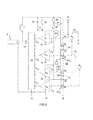
FIGS. 4-6 ,exemplary frontend portions 2 are shown which include N antennas A1, A2... AN (e.g., N = 4), each antenna being optimized for a specific frequency band and antenna amplifiers V1, V2... VN that are, together with input capacitors CI1 .. CIN and output capacitors CO1 .. CON, each connected between one of the N (= 4) antennas and acombiner network 18. Thecombiner network 18 may be a passive network and is connected to thefeed line 3 through acapacitor 16 that forms together with aninductor 17 and a capacitor 19 a splitter network. Theinductor 17 connects thefeed line 3 to a first terminal of acapacitor 19 whose second terminal is connected to groundG. A resistor 20, which forms part of the internal resistance Ri, is connected in parallel tocapacitor 19. - Referring now to
FIG. 4 , thefront end portion 2, which may cooperate with thebackend portion 1 as described above in connection withFIG. 2 , further includes tworesistors jumpers jumpers antenna plug 29; 32; 33, 36 and at least twojumper plugs rear window 26 of an automobile. Thejumpers frontend portion 2 by way of the plugs 27-36 which engage with corresponding jacks (not shown) in order to provide (detachable) electrical connections. Antenna plugs 29, 32, 33 and 36 (with corresponding jacks) serve to connect the N (= 4) antennas A1, A2 ... AN to the antenna amplifiers V1, V2 ... VN via input capacitors CI1 ... CIN. The antenna amplifiers V1, V2 ... VN are connected in parallel in terms of supply lines, i.e., first supply lines of antenna amplifiers V1, V2 ... VN are connected to ground G and second supply lines are connected tojumper plug 35 ofjumper 25 whoseother jumper plug 34 is connected tojumper plug 31 ofjumper 24 and throughresistor 22 to ground G. Jumperplug 30 ofjumper 24 is connected tojumper plug 28 ofjumper 23 and through aresistor 21 to ground G. Jumperplug 27 ofjumper 23 is connected to the first terminal ofcapacitor 19. - If any one of the multi-plug antenna connectors AC1, AC2 and AC3 is pulled off, broken or otherwise disconnected, the supply chain for all antenna amplifiers V1, V2 ... VN is interrupted and no power is consumed by the antenna amplifiers V1, V2 ... VN. In this case, the internal resistance Ri is determined by the resistance R20 of
resistor 20 and, depending on which one of thejumpers resistors jumper 23 which corresponds to antenna A1 is disconnected, then 1/Ri = 1/R20. Ifjumper 24 which corresponds to antenna A2 is disconnected, then 1/Ri = 1/R20 + 1/R21. Ifjumper 25 which corresponds to antennas A3 and A4 is disconnected, then 1/Ri = 1/R20 + 1/R21+ 1/R22. Assuming, as an example, thatresistors - Ri = R, when
jumper 23 is disconnected, i.e., antenna A1 is disconnected; - Ri = R/2, when
jumper 24 is disconnected, i.e., antenna A2 is disconnected; - Ri = R/3, when
jumper 25 is disconnected, i.e., antennas A3 and A4 are disconnected. - The resistance of the antenna amplifiers V1, V2 ... VN may be, for instance, less than R/10. If none of the
jumpers FIG. 2 ) measures the internal resistance Ri of thefrontend portion 2 and determines by way of the measured internal resistance Ri the status of thefrontend portion 2. - Referring to
FIG. 5 , thefront end portion 2, which may cooperate with thebackend portions 1 as described above in connection withFIGS. 2 and 3 , employs a controllable switch 37-39 and twoinductances jumper 23 and theresistor 21 in thefrontend portion 2 ofFIG. 4 . The antenna plugs 29, 32 and thejumper 24 including jumper plugs 30, 31 are integrated in a multi-plug antenna connector AC4 and antenna connectors AC1, AC2 have been omitted. The controllable switch 37-39 includes a transistor, e.g., pnpbipolar transistor 37 which has base, collector and emitter terminals. The emitter and base terminals are connected to each other by way of aresistor 38, and the base terminal is further connected through aresistor 39 and theinductance 40 to thecontact element 29. Theinductance 41 couples contactelement 29 with ground G in terms of DC and may be integrated in therear window 26. As there is nojumper plug 23, correspondingcontact elements - The controllable switch 37-39 is switched on when
contact element 29 is in an operating condition, as in this case the base terminal oftransistor 37 is connected to ground G viacontact element 29,resistor 39 andinductances particular jumpers FIG. 4 . -
FIG. 6 illustrates modifications in thefront end portion 2 ofFIG. 5 . Thefront end portion 2 shown inFIG. 6 may cooperate with thebackend portion 1 as described above in connection withFIG. 3 . Therear window 26 and the antenna connectors AC3, AC4 are the same as in the example ofFIG. 5 , however, the external wiring of the jumper plugs 30, 31, 34, 35 is different. Jumper plugs 35 and 31 are connected to ground G and jumper plugs 34 and 30 are connected through aresistor 42 and 43 to the first terminal ofcapacitor 19. The series-connectedresistors frontend portion 2 ofFIG. 5 are substituted by asingle resistor 44.Resistor 20 andtransistor 37 are omitted. The second supply lines of antenna amplifiers V1, V2 ... VN are connected to the collector terminal of a pnpbipolar transistor 45 whose emitter terminal is connected to the first terminal ofcapacitor 19. Aresistor 46 is connected between the base terminal oftransistor 45 and the first terminal ofcapacitor 19. Furthermore, aresistor 47 and a series connected reference voltage element, e.g., aZener diode 48, are connected between the base terminal oftransistor 45 and ground G. - The
transistor 45 in connection with theZener diode 48 and theresistors frontend portion 2 is larger by a certain amount than a reference voltage provided by theZener diode 48. Otherwise it is switched off. When combined with, e.g., thebackend portion 1 shown inFIG. 3 , thefrontend portion 2 may be switched into an operating mode or a test mode dependant on the voltage supplied to thefrontend portion 2. In the present example, the test mode is active when a voltage sufficient lower than in the operating mode is provided by thebackend portion 1. - In the backend portion1 of
FIG. 3 , the test mode is established by a constant current supply from current source 10 (i.e., switch 15 is in a non-conducting state). This constant current generates across the internal resistance Ri a supply voltage that controls the controllable switch 45-48 such that it switches off. Whenswitch 15 is in a conducting state, the full voltage is supplied to thefrontend portion 2 which turns the controllable switch into an on-state. Accordingly, in the test mode all antenna amplifiers V1, V2 ... VN are switched off, i.e., inactive, and the internal resistance Ri is mainly dependant on the resistors 42-4 and which one of thejumpers jumper 24 indicates thatantenna plug jumper 25 indicates that antenna plugs 33 and 36 are operable. When antenna plug 29 is operable,resistor 44 is connected to ground G thereby decreasing the internal resistance Ri. With an adequate choice of resistance values for resistors 42-44, it can be detected by measuring the internal resistance Ri which one of the antennas is not connected. For instance, an adequate choice may be R, R/2 and R/4. Instead of jumpers, switches may be used which may be arranged in mechanical contact with, e.g., integrated in the connectors, which may be integrated in the rear window. - It will be obvious to those reasonably skilled in the art that other components performing the same functions may be suitably substituted. Such modifications to the concept disclosed herein are intended to be covered by the appended claims.
Claims (14)
- An antenna system comprising a frontend portion, a backend portion and a feed line which connects the frontend portion and backend portion with each other, in which:the frontend portion comprises at least two antennas, a combiner circuit connected downstream of the antennas and upstream of the feed line and antenna connectors that electrically connect through antenna plugs the antennas to the combiner;the backend portion comprises an electrical power source connected to the feed line and a resistance evaluation circuit that is connected between the power voltage source and the feed line and that measures the resistance of the frontend portion through the feed line;at least one of the antenna connectors is in mechanical contact with a jumper having jumper plugs between which a higher resistance connection and a lower resistance connection is provided dependent on whether the corresponding antenna is connected to the combiner or not; the jumper plugs are connected to the feed line such that the internal resistance of the frontend portion depends on whether the corresponding antenna is connected to the combiner or not; andthe resistance evaluation circuit is configured to detect whether one of the antennas is not connected to the corresponding antenna signal amplifier by evaluating the resistance of the frontend portion.
- The antenna system of claim 1, in which at least one of the connectors is partly or in total removable.
- The antenna system of claim 2, in which at least one antenna connector comprises a jumper that is integrated in the at least one antenna connector so that the jumper is removed when the removable connector is removed.
- The antenna system of claim 1, 2 or 3, in which resistors are connected in series or in parallel to at least one of the jumpers.
- The antenna system of claim 4, in which at least two resistors are connected in series or in parallel when the at least one jumper is in place.
- The antenna system of one of the preceding claims, in which at least one of the antennas or the jumpers is integrated in a pane of glass.
- The antenna system of one of the preceding claims, in which the jumpers are electrically connected such that, if one of the jumpers is removed, the antenna amplifiers become inactive.
- The antenna system of one of the preceding claims, in which the backend portion comprises as a power source a constant voltage source and a current measuring circuit for evaluating the internal resistance of the frontend portion.
- The antenna system of one of the preceding claims, in which the backend portion comprises as a power source a constant current source and a voltage measuring circuit for evaluating the internal resistance of the frontend portion.
- The antenna system of one of the preceding claims, in which at least one of the resistors contributing to the internal resistance of the frontend portion is connected via a first and a second inductor and one of the connectors to the feed line.
- The antenna system of claim 10, further comprising a controllable switch the frontend portion that is controlled by a voltage across or a current through from the backend portion.
- The antenna system of one of the preceding claims, in which the backend portion provides different voltages to the frontend portion in an operating mode and in a test mode.
- The antenna system of one of claims 1-11, in which the backend portion provides a constant voltage in the operating mode and a constant current in the test mode.
- The antenna system of claim 12 or 13, in which the front end portion has a controllable switch that inactivates the antenna amplifiers when the backend portion is in a test mode.
Priority Applications (4)
| Application Number | Priority Date | Filing Date | Title |
|---|---|---|---|
| EP12178319.5A EP2690793B1 (en) | 2012-07-27 | 2012-07-27 | Multiple-antenna system |
| CN201310251480.4A CN103580735B (en) | 2012-07-27 | 2013-06-24 | Multiaerial system |
| KR1020130078120A KR102007931B1 (en) | 2012-07-27 | 2013-07-04 | Multiple-antenna system |
| US13/950,802 US9147937B2 (en) | 2012-07-27 | 2013-07-25 | Multiple-antenna system |
Applications Claiming Priority (1)
| Application Number | Priority Date | Filing Date | Title |
|---|---|---|---|
| EP12178319.5A EP2690793B1 (en) | 2012-07-27 | 2012-07-27 | Multiple-antenna system |
Publications (2)
| Publication Number | Publication Date |
|---|---|
| EP2690793A1 true EP2690793A1 (en) | 2014-01-29 |
| EP2690793B1 EP2690793B1 (en) | 2015-07-01 |
Family
ID=46650388
Family Applications (1)
| Application Number | Title | Priority Date | Filing Date |
|---|---|---|---|
| EP12178319.5A Active EP2690793B1 (en) | 2012-07-27 | 2012-07-27 | Multiple-antenna system |
Country Status (4)
| Country | Link |
|---|---|
| US (1) | US9147937B2 (en) |
| EP (1) | EP2690793B1 (en) |
| KR (1) | KR102007931B1 (en) |
| CN (1) | CN103580735B (en) |
Cited By (1)
| Publication number | Priority date | Publication date | Assignee | Title |
|---|---|---|---|---|
| CN109103591A (en) * | 2018-08-16 | 2018-12-28 | 昆山恩电开通信设备有限公司 | A kind of radiating element with space wave transparent characteristic |
Families Citing this family (6)
| Publication number | Priority date | Publication date | Assignee | Title |
|---|---|---|---|---|
| DE102015002245B3 (en) * | 2015-02-21 | 2016-05-25 | Audi Ag | Method for operating a radio system, radio system and motor vehicle with a radio system |
| US10348420B2 (en) * | 2016-06-28 | 2019-07-09 | Marek E. Antkowiak | Antenna status remote monitoring system |
| CN111264034A (en) * | 2017-10-25 | 2020-06-09 | 日本精机株式会社 | Receiving circuit and communication device |
| EP3776038B1 (en) | 2018-03-28 | 2024-07-03 | Senko Advanced Components Inc. | Small form factor fiber optic connector with multi-purpose boot |
| DE102018206339A1 (en) * | 2018-04-25 | 2019-10-31 | Continental Automotive Gmbh | Device and method for functional testing of an antenna system for detecting foreign metal |
| FR3144367B1 (en) * | 2022-12-23 | 2025-12-26 | Banks And Acquirers Int Holding | Method for determining the condition of an antenna |
Citations (4)
| Publication number | Priority date | Publication date | Assignee | Title |
|---|---|---|---|---|
| DE4130608C1 (en) * | 1991-09-14 | 1992-08-13 | Grundig E.M.V. Elektro-Mechanische Versuchsanstalt Max Grundig Hollaend. Stiftung & Co Kg, 8510 Fuerth, De | DC power supply unit for antenna amplifier - measures impedance seen at receiver and switches off power supply voltage when impedance value indicates fault or short circuit |
| US20040116084A1 (en) * | 2002-12-12 | 2004-06-17 | Ward Dennis Paul | Active antenna system with fault detection |
| US20060145884A1 (en) * | 2004-12-27 | 2006-07-06 | P. G. Electronics Ltd. | Fault monitoring in a distributed antenna system |
| US20070152675A1 (en) * | 2003-12-20 | 2007-07-05 | Michael Thole | Diagnostic method for monitoring a plug-in connection |
Family Cites Families (12)
| Publication number | Priority date | Publication date | Assignee | Title |
|---|---|---|---|---|
| US5649308A (en) | 1993-04-12 | 1997-07-15 | Trw Inc. | Multiformat auto-handoff communications handset |
| AU714193B2 (en) * | 1996-03-13 | 1999-12-23 | Wi-Lan, Inc. | Wireless communication device with antenna-activated switch |
| JP2000114856A (en) * | 1998-09-30 | 2000-04-21 | Nec Saitama Ltd | Reversed f antenna and radio equipment using the same |
| DE19923729A1 (en) | 1999-05-22 | 2000-11-23 | Nokia Mobile Phones Ltd | Circuit arrangement for checking the operational readiness of at least one antenna |
| DE10033336A1 (en) * | 1999-08-11 | 2001-04-12 | Heinz Lindenmeier | Diversity antenna for diversity system in vehicle has edge conductor on side of conducting surface with minimum length of about tenth of wavelength, forming low impedance coupling line |
| US7386284B2 (en) * | 2004-12-01 | 2008-06-10 | Silicon Laboratories Inc. | Controlling the gain of a remote active antenna |
| US20060205369A1 (en) | 2005-03-06 | 2006-09-14 | Hirschmann Car Communication Gmbh | Multiple antenna receiver system in vehicles |
| US7652634B2 (en) * | 2005-09-01 | 2010-01-26 | Dell Products L.P. | Antenna with integrated parameter storage |
| KR100857138B1 (en) * | 2006-04-28 | 2008-09-05 | 엘지전자 주식회사 | Antenna system and electronic device including same |
| US7277056B1 (en) | 2006-09-15 | 2007-10-02 | Laird Technologies, Inc. | Stacked patch antennas |
| DE102008048986B4 (en) * | 2008-09-25 | 2019-03-14 | Atmel Corp. | Antenna amplifier and receiving system |
| CN102484490A (en) | 2009-09-04 | 2012-05-30 | 莱尔德技术股份有限公司 | Antenna device and portable wireless communication device including the antenna device |
-
2012
- 2012-07-27 EP EP12178319.5A patent/EP2690793B1/en active Active
-
2013
- 2013-06-24 CN CN201310251480.4A patent/CN103580735B/en active Active
- 2013-07-04 KR KR1020130078120A patent/KR102007931B1/en active Active
- 2013-07-25 US US13/950,802 patent/US9147937B2/en active Active
Patent Citations (4)
| Publication number | Priority date | Publication date | Assignee | Title |
|---|---|---|---|---|
| DE4130608C1 (en) * | 1991-09-14 | 1992-08-13 | Grundig E.M.V. Elektro-Mechanische Versuchsanstalt Max Grundig Hollaend. Stiftung & Co Kg, 8510 Fuerth, De | DC power supply unit for antenna amplifier - measures impedance seen at receiver and switches off power supply voltage when impedance value indicates fault or short circuit |
| US20040116084A1 (en) * | 2002-12-12 | 2004-06-17 | Ward Dennis Paul | Active antenna system with fault detection |
| US20070152675A1 (en) * | 2003-12-20 | 2007-07-05 | Michael Thole | Diagnostic method for monitoring a plug-in connection |
| US20060145884A1 (en) * | 2004-12-27 | 2006-07-06 | P. G. Electronics Ltd. | Fault monitoring in a distributed antenna system |
Cited By (2)
| Publication number | Priority date | Publication date | Assignee | Title |
|---|---|---|---|---|
| CN109103591A (en) * | 2018-08-16 | 2018-12-28 | 昆山恩电开通信设备有限公司 | A kind of radiating element with space wave transparent characteristic |
| CN109103591B (en) * | 2018-08-16 | 2023-09-22 | 昆山恩电开通信设备有限公司 | Radiating element with space wave-transmitting characteristic |
Also Published As
| Publication number | Publication date |
|---|---|
| US9147937B2 (en) | 2015-09-29 |
| KR20140013921A (en) | 2014-02-05 |
| CN103580735A (en) | 2014-02-12 |
| CN103580735B (en) | 2018-06-15 |
| KR102007931B1 (en) | 2019-08-06 |
| EP2690793B1 (en) | 2015-07-01 |
| US20140028527A1 (en) | 2014-01-30 |
Similar Documents
| Publication | Publication Date | Title |
|---|---|---|
| EP2690793B1 (en) | Multiple-antenna system | |
| US10455510B2 (en) | Interface device providing power management and load termination in distributed antenna system | |
| US9188645B2 (en) | System and method for testing a circuit | |
| US11852658B2 (en) | Measurement input circuit and measurement device | |
| KR101774143B1 (en) | Unpowered switching module | |
| EP2560294A1 (en) | Impedance stabilization device | |
| US11043978B2 (en) | Bidirectional coupler | |
| CN109687913A (en) | Wireless communication unit diagnosis | |
| EP2743712B1 (en) | Testing device and method of testing | |
| CN110658391B (en) | Auxiliary test device and test method for electromagnetic compatibility | |
| US20100295569A1 (en) | Rf performance test structure with electronic switch function | |
| EP3195504B1 (en) | Monitoring system for a distributed antenna system | |
| US8027648B2 (en) | Radio frequency power monitor | |
| US8384399B2 (en) | System including capacitively coupled electrodes and circuits in a network | |
| EP3855627B1 (en) | Amplifier module | |
| JP6220384B2 (en) | Power supply circuit device for supplying radio frequency signals to a plurality of coil elements of a magnetic resonance coil system | |
| CN106568471B (en) | Sensor power supply and signal adjusting interface of machine state monitoring system | |
| CN108282172B (en) | Power adapter | |
| KR101769607B1 (en) | Patch Panel | |
| US12519499B2 (en) | Short detection and protection circuit for access point | |
| US20230139159A1 (en) | Automotive Controller Testing | |
| JP4213552B2 (en) | External antenna detection circuit, wireless device and external antenna switching circuit | |
| US11569869B2 (en) | Transceiving circuit | |
| CN211426640U (en) | Auxiliary test device for electromagnetic compatibility | |
| US20060146942A1 (en) | Arrangement for compensation of ground offset in a data bus system |
Legal Events
| Date | Code | Title | Description |
|---|---|---|---|
| PUAI | Public reference made under article 153(3) epc to a published international application that has entered the european phase |
Free format text: ORIGINAL CODE: 0009012 |
|
| AK | Designated contracting states |
Kind code of ref document: A1 Designated state(s): AL AT BE BG CH CY CZ DE DK EE ES FI FR GB GR HR HU IE IS IT LI LT LU LV MC MK MT NL NO PL PT RO RS SE SI SK SM TR |
|
| AX | Request for extension of the european patent |
Extension state: BA ME |
|
| 17P | Request for examination filed |
Effective date: 20140722 |
|
| RBV | Designated contracting states (corrected) |
Designated state(s): AL AT BE BG CH CY CZ DE DK EE ES FI FR GB GR HR HU IE IS IT LI LT LU LV MC MK MT NL NO PL PT RO RS SE SI SK SM TR |
|
| GRAP | Despatch of communication of intention to grant a patent |
Free format text: ORIGINAL CODE: EPIDOSNIGR1 |
|
| RIC1 | Information provided on ipc code assigned before grant |
Ipc: H04B 1/00 20060101AFI20141128BHEP Ipc: H04B 17/00 20150101ALI20141128BHEP Ipc: H04B 1/04 20060101ALI20141128BHEP |
|
| INTG | Intention to grant announced |
Effective date: 20141215 |
|
| GRAS | Grant fee paid |
Free format text: ORIGINAL CODE: EPIDOSNIGR3 |
|
| GRAA | (expected) grant |
Free format text: ORIGINAL CODE: 0009210 |
|
| AK | Designated contracting states |
Kind code of ref document: B1 Designated state(s): AL AT BE BG CH CY CZ DE DK EE ES FI FR GB GR HR HU IE IS IT LI LT LU LV MC MK MT NL NO PL PT RO RS SE SI SK SM TR |
|
| REG | Reference to a national code |
Ref country code: GB Ref legal event code: FG4D |
|
| REG | Reference to a national code |
Ref country code: AT Ref legal event code: REF Ref document number: 734485 Country of ref document: AT Kind code of ref document: T Effective date: 20150715 Ref country code: CH Ref legal event code: EP |
|
| REG | Reference to a national code |
Ref country code: IE Ref legal event code: FG4D |
|
| REG | Reference to a national code |
Ref country code: DE Ref legal event code: R096 Ref document number: 602012008329 Country of ref document: DE |
|
| REG | Reference to a national code |
Ref country code: AT Ref legal event code: MK05 Ref document number: 734485 Country of ref document: AT Kind code of ref document: T Effective date: 20150701 |
|
| REG | Reference to a national code |
Ref country code: NL Ref legal event code: MP Effective date: 20150701 |
|
| REG | Reference to a national code |
Ref country code: LT Ref legal event code: MG4D |
|
| PG25 | Lapsed in a contracting state [announced via postgrant information from national office to epo] |
Ref country code: LT Free format text: LAPSE BECAUSE OF FAILURE TO SUBMIT A TRANSLATION OF THE DESCRIPTION OR TO PAY THE FEE WITHIN THE PRESCRIBED TIME-LIMIT Effective date: 20150701 Ref country code: FI Free format text: LAPSE BECAUSE OF FAILURE TO SUBMIT A TRANSLATION OF THE DESCRIPTION OR TO PAY THE FEE WITHIN THE PRESCRIBED TIME-LIMIT Effective date: 20150701 Ref country code: LV Free format text: LAPSE BECAUSE OF FAILURE TO SUBMIT A TRANSLATION OF THE DESCRIPTION OR TO PAY THE FEE WITHIN THE PRESCRIBED TIME-LIMIT Effective date: 20150701 Ref country code: NO Free format text: LAPSE BECAUSE OF FAILURE TO SUBMIT A TRANSLATION OF THE DESCRIPTION OR TO PAY THE FEE WITHIN THE PRESCRIBED TIME-LIMIT Effective date: 20151001 Ref country code: GR Free format text: LAPSE BECAUSE OF FAILURE TO SUBMIT A TRANSLATION OF THE DESCRIPTION OR TO PAY THE FEE WITHIN THE PRESCRIBED TIME-LIMIT Effective date: 20151002 |
|
| PG25 | Lapsed in a contracting state [announced via postgrant information from national office to epo] |
Ref country code: PT Free format text: LAPSE BECAUSE OF FAILURE TO SUBMIT A TRANSLATION OF THE DESCRIPTION OR TO PAY THE FEE WITHIN THE PRESCRIBED TIME-LIMIT Effective date: 20151102 Ref country code: PL Free format text: LAPSE BECAUSE OF FAILURE TO SUBMIT A TRANSLATION OF THE DESCRIPTION OR TO PAY THE FEE WITHIN THE PRESCRIBED TIME-LIMIT Effective date: 20150701 Ref country code: SE Free format text: LAPSE BECAUSE OF FAILURE TO SUBMIT A TRANSLATION OF THE DESCRIPTION OR TO PAY THE FEE WITHIN THE PRESCRIBED TIME-LIMIT Effective date: 20150701 Ref country code: RS Free format text: LAPSE BECAUSE OF FAILURE TO SUBMIT A TRANSLATION OF THE DESCRIPTION OR TO PAY THE FEE WITHIN THE PRESCRIBED TIME-LIMIT Effective date: 20150701 Ref country code: HR Free format text: LAPSE BECAUSE OF FAILURE TO SUBMIT A TRANSLATION OF THE DESCRIPTION OR TO PAY THE FEE WITHIN THE PRESCRIBED TIME-LIMIT Effective date: 20150701 Ref country code: ES Free format text: LAPSE BECAUSE OF FAILURE TO SUBMIT A TRANSLATION OF THE DESCRIPTION OR TO PAY THE FEE WITHIN THE PRESCRIBED TIME-LIMIT Effective date: 20150701 Ref country code: AT Free format text: LAPSE BECAUSE OF FAILURE TO SUBMIT A TRANSLATION OF THE DESCRIPTION OR TO PAY THE FEE WITHIN THE PRESCRIBED TIME-LIMIT Effective date: 20150701 Ref country code: IS Free format text: LAPSE BECAUSE OF FAILURE TO SUBMIT A TRANSLATION OF THE DESCRIPTION OR TO PAY THE FEE WITHIN THE PRESCRIBED TIME-LIMIT Effective date: 20151101 |
|
| REG | Reference to a national code |
Ref country code: CH Ref legal event code: PL |
|
| PG25 | Lapsed in a contracting state [announced via postgrant information from national office to epo] |
Ref country code: MC Free format text: LAPSE BECAUSE OF FAILURE TO SUBMIT A TRANSLATION OF THE DESCRIPTION OR TO PAY THE FEE WITHIN THE PRESCRIBED TIME-LIMIT Effective date: 20150701 |
|
| REG | Reference to a national code |
Ref country code: DE Ref legal event code: R097 Ref document number: 602012008329 Country of ref document: DE |
|
| REG | Reference to a national code |
Ref country code: IE Ref legal event code: MM4A |
|
| PG25 | Lapsed in a contracting state [announced via postgrant information from national office to epo] |
Ref country code: EE Free format text: LAPSE BECAUSE OF FAILURE TO SUBMIT A TRANSLATION OF THE DESCRIPTION OR TO PAY THE FEE WITHIN THE PRESCRIBED TIME-LIMIT Effective date: 20150701 Ref country code: IT Free format text: LAPSE BECAUSE OF FAILURE TO SUBMIT A TRANSLATION OF THE DESCRIPTION OR TO PAY THE FEE WITHIN THE PRESCRIBED TIME-LIMIT Effective date: 20150701 Ref country code: CH Free format text: LAPSE BECAUSE OF NON-PAYMENT OF DUE FEES Effective date: 20150731 Ref country code: LI Free format text: LAPSE BECAUSE OF NON-PAYMENT OF DUE FEES Effective date: 20150731 Ref country code: CZ Free format text: LAPSE BECAUSE OF FAILURE TO SUBMIT A TRANSLATION OF THE DESCRIPTION OR TO PAY THE FEE WITHIN THE PRESCRIBED TIME-LIMIT Effective date: 20150701 Ref country code: DK Free format text: LAPSE BECAUSE OF FAILURE TO SUBMIT A TRANSLATION OF THE DESCRIPTION OR TO PAY THE FEE WITHIN THE PRESCRIBED TIME-LIMIT Effective date: 20150701 Ref country code: SK Free format text: LAPSE BECAUSE OF FAILURE TO SUBMIT A TRANSLATION OF THE DESCRIPTION OR TO PAY THE FEE WITHIN THE PRESCRIBED TIME-LIMIT Effective date: 20150701 |
|
| PLBE | No opposition filed within time limit |
Free format text: ORIGINAL CODE: 0009261 |
|
| STAA | Information on the status of an ep patent application or granted ep patent |
Free format text: STATUS: NO OPPOSITION FILED WITHIN TIME LIMIT |
|
| PG25 | Lapsed in a contracting state [announced via postgrant information from national office to epo] |
Ref country code: RO Free format text: LAPSE BECAUSE OF FAILURE TO SUBMIT A TRANSLATION OF THE DESCRIPTION OR TO PAY THE FEE WITHIN THE PRESCRIBED TIME-LIMIT Effective date: 20150701 |
|
| 26N | No opposition filed |
Effective date: 20160404 |
|
| PG25 | Lapsed in a contracting state [announced via postgrant information from national office to epo] |
Ref country code: IE Free format text: LAPSE BECAUSE OF NON-PAYMENT OF DUE FEES Effective date: 20150727 |
|
| PG25 | Lapsed in a contracting state [announced via postgrant information from national office to epo] |
Ref country code: SI Free format text: LAPSE BECAUSE OF FAILURE TO SUBMIT A TRANSLATION OF THE DESCRIPTION OR TO PAY THE FEE WITHIN THE PRESCRIBED TIME-LIMIT Effective date: 20150701 |
|
| REG | Reference to a national code |
Ref country code: FR Ref legal event code: ST Effective date: 20160805 |
|
| PG25 | Lapsed in a contracting state [announced via postgrant information from national office to epo] |
Ref country code: FR Free format text: LAPSE BECAUSE OF NON-PAYMENT OF DUE FEES Effective date: 20150901 |
|
| PG25 | Lapsed in a contracting state [announced via postgrant information from national office to epo] |
Ref country code: BE Free format text: LAPSE BECAUSE OF FAILURE TO SUBMIT A TRANSLATION OF THE DESCRIPTION OR TO PAY THE FEE WITHIN THE PRESCRIBED TIME-LIMIT Effective date: 20150701 |
|
| GBPC | Gb: european patent ceased through non-payment of renewal fee |
Effective date: 20160727 |
|
| PG25 | Lapsed in a contracting state [announced via postgrant information from national office to epo] |
Ref country code: MT Free format text: LAPSE BECAUSE OF FAILURE TO SUBMIT A TRANSLATION OF THE DESCRIPTION OR TO PAY THE FEE WITHIN THE PRESCRIBED TIME-LIMIT Effective date: 20150701 |
|
| PG25 | Lapsed in a contracting state [announced via postgrant information from national office to epo] |
Ref country code: BG Free format text: LAPSE BECAUSE OF FAILURE TO SUBMIT A TRANSLATION OF THE DESCRIPTION OR TO PAY THE FEE WITHIN THE PRESCRIBED TIME-LIMIT Effective date: 20150701 Ref country code: HU Free format text: LAPSE BECAUSE OF FAILURE TO SUBMIT A TRANSLATION OF THE DESCRIPTION OR TO PAY THE FEE WITHIN THE PRESCRIBED TIME-LIMIT; INVALID AB INITIO Effective date: 20120727 Ref country code: GB Free format text: LAPSE BECAUSE OF NON-PAYMENT OF DUE FEES Effective date: 20160727 Ref country code: SM Free format text: LAPSE BECAUSE OF FAILURE TO SUBMIT A TRANSLATION OF THE DESCRIPTION OR TO PAY THE FEE WITHIN THE PRESCRIBED TIME-LIMIT Effective date: 20150701 |
|
| PG25 | Lapsed in a contracting state [announced via postgrant information from national office to epo] |
Ref country code: NL Free format text: LAPSE BECAUSE OF FAILURE TO SUBMIT A TRANSLATION OF THE DESCRIPTION OR TO PAY THE FEE WITHIN THE PRESCRIBED TIME-LIMIT Effective date: 20150701 Ref country code: CY Free format text: LAPSE BECAUSE OF FAILURE TO SUBMIT A TRANSLATION OF THE DESCRIPTION OR TO PAY THE FEE WITHIN THE PRESCRIBED TIME-LIMIT Effective date: 20150701 |
|
| PG25 | Lapsed in a contracting state [announced via postgrant information from national office to epo] |
Ref country code: LU Free format text: LAPSE BECAUSE OF NON-PAYMENT OF DUE FEES Effective date: 20150727 |
|
| PG25 | Lapsed in a contracting state [announced via postgrant information from national office to epo] |
Ref country code: MK Free format text: LAPSE BECAUSE OF FAILURE TO SUBMIT A TRANSLATION OF THE DESCRIPTION OR TO PAY THE FEE WITHIN THE PRESCRIBED TIME-LIMIT Effective date: 20150701 Ref country code: TR Free format text: LAPSE BECAUSE OF FAILURE TO SUBMIT A TRANSLATION OF THE DESCRIPTION OR TO PAY THE FEE WITHIN THE PRESCRIBED TIME-LIMIT Effective date: 20150701 |
|
| PG25 | Lapsed in a contracting state [announced via postgrant information from national office to epo] |
Ref country code: AL Free format text: LAPSE BECAUSE OF FAILURE TO SUBMIT A TRANSLATION OF THE DESCRIPTION OR TO PAY THE FEE WITHIN THE PRESCRIBED TIME-LIMIT Effective date: 20150701 |
|
| P01 | Opt-out of the competence of the unified patent court (upc) registered |
Effective date: 20230526 |
|
| PGFP | Annual fee paid to national office [announced via postgrant information from national office to epo] |
Ref country code: DE Payment date: 20250620 Year of fee payment: 14 |