EP2690704A1 - Transmission line for mobile electronic device - Google Patents
Transmission line for mobile electronic device Download PDFInfo
- Publication number
- EP2690704A1 EP2690704A1 EP20120177616 EP12177616A EP2690704A1 EP 2690704 A1 EP2690704 A1 EP 2690704A1 EP 20120177616 EP20120177616 EP 20120177616 EP 12177616 A EP12177616 A EP 12177616A EP 2690704 A1 EP2690704 A1 EP 2690704A1
- Authority
- EP
- European Patent Office
- Prior art keywords
- electronic device
- mobile electronic
- conductive
- electrical ground
- short
- Prior art date
- Legal status (The legal status is an assumption and is not a legal conclusion. Google has not performed a legal analysis and makes no representation as to the accuracy of the status listed.)
- Granted
Links
Images





Classifications
-
- H—ELECTRICITY
- H01—ELECTRIC ELEMENTS
- H01Q—ANTENNAS, i.e. RADIO AERIALS
- H01Q1/00—Details of, or arrangements associated with, antennas
- H01Q1/12—Supports; Mounting means
- H01Q1/22—Supports; Mounting means by structural association with other equipment or articles
- H01Q1/24—Supports; Mounting means by structural association with other equipment or articles with receiving set
- H01Q1/241—Supports; Mounting means by structural association with other equipment or articles with receiving set used in mobile communications, e.g. GSM
- H01Q1/242—Supports; Mounting means by structural association with other equipment or articles with receiving set used in mobile communications, e.g. GSM specially adapted for hand-held use
- H01Q1/243—Supports; Mounting means by structural association with other equipment or articles with receiving set used in mobile communications, e.g. GSM specially adapted for hand-held use with built-in antennas
-
- H—ELECTRICITY
- H01—ELECTRIC ELEMENTS
- H01Q—ANTENNAS, i.e. RADIO AERIALS
- H01Q1/00—Details of, or arrangements associated with, antennas
- H01Q1/48—Earthing means; Earth screens; Counterpoises
-
- H—ELECTRICITY
- H01—ELECTRIC ELEMENTS
- H01Q—ANTENNAS, i.e. RADIO AERIALS
- H01Q5/00—Arrangements for simultaneous operation of antennas on two or more different wavebands, e.g. dual-band or multi-band arrangements
- H01Q5/30—Arrangements for providing operation on different wavebands
- H01Q5/378—Combination of fed elements with parasitic elements
Definitions
- the specification relates generally to mobile electronic devices, and specifically to a transmission line for a mobile electronic device.
- Mobile electronic devices such as smartphones, are generally becoming more compact.
- smartphones are generally becoming more compact.
- the housings of smartphones can include metal components which also interfere with antenna performance.
- the introduction of network technologies such as LTE, which employ lower frequencies, can heighten the difficulties in obtaining acceptable performance from smaller antennas.
- a mobile electronic device comprising: an electrical ground member supporting at least one antenna; a housing containing the electrical ground member and having a conductive ring defining the perimeter of the housing; and a conductive tuning member disposed between the conductive ring and the electrical ground member, for transforming an impedance between the electrical ground member and the conductive ring; wherein the conductive tuning member is connected to the conductive ring by a first short, and to the electrical ground member by a second short.
- a method comprising: fastening a conductive tuning member between a conductive ring defining a perimeter of a housing of a mobile electronic device, and an electrical ground member contained within the housing; selecting a first short location for connecting the conductive tuning member to the conductive ring; and selecting a second short location for connecting the conductive tuning member to the electrical ground member.
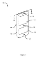
- Figure 1 depicts a mobile electronic device, according to a non-limiting embodiment
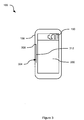
- Figure 2 depicts certain internal components of the mobile electronic device of Figure 1 , according to a non-limiting embodiment
- Figure 3 depicts a cross sectional view of the mobile electronic device of Figure 1 , according to a non-limiting embodiment
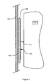
- Figure 4 depicts a partial view of the cross section of Figure 3 , according to a non-limiting embodiment
- Figure 5 depicts the open space performance of an antenna of the device of Figure 1 , according to a non-limiting embodiment
- Figure 6 depicts the performance of the antenna of the device of Figure 1 when installed in the device of Figure 1 , according to a non-limiting embodiment
- Figure 7 depicts the performance of the antenna of the device of Figure 1 when a conductive tuning member is provided, according to a non-limiting embodiment
- Figure 8 depicts the conductive tuning member of Figure 4 , according to a non-limiting embodiment.
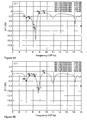
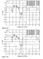
- Figures 9A, 9B , 10A, 10B , 11A, 11B and 12 depict the performance of the antenna of the device of Figure 1 for various configurations of the conductive tuning member of Figure 4 , according to a non-limiting embodiment.
- FIG. 1 depicts a mobile electronic device 100, which in the present embodiment is based on the computing environment and functionality of a hand-held wireless communication device. It will be understood, however, that mobile electronic device 100 is not limited to a hand-held wireless communication device. Other mobile electronic devices are also contemplated, such as cellular phones, smart phones, Personal Digital Assistants ("PDAs”), media or MP3 players, tablet computers, laptop computers, and the like.
- PDAs Personal Digital Assistants
- Mobile electronic device 100 includes a housing 104 which supports the various other components of mobile electronic device 100.
- Housing 104 includes a conductive (that is, electrically conductive) ring 108 (also referred to herein simply as "ring 108") defining the perimeter of housing 104.
- ring 108 extends continuously around the perimeter of housing 104.
- Ring 108 can be constructed of any electrically conductive material, including any one or combination of aluminum and other metals.
- the remaining portion of housing 104 can be constructed of any suitable material, or combination of materials, including without limitation plastics (e.g. Polycarbonate/Acrylonitrile Butadiene Styrene (“PC/ABS”)) and metals (e.g. aluminum or other metals).
- PC/ABS Polycarbonate/Acrylonitrile Butadiene Styrene
- Mobile electronic device 100 also includes one or more output devices, including without limitation a display 112 and a speaker 116.
- output devices including without limitation a display 112 and a speaker 116.
- Other output devices are also contemplated but not shown, such as a Light Emitting Diode (LED) indicator, a vibrating motor, and the like.
- LED Light Emitting Diode
- Mobile electronic device 100 additionally includes one or more input devices, including without limitation a microphone 120, a keypad 124.
- Keypad 124 can be a full QWERTY keyboard or a reduced QWERTY keyboard.
- Mobile electronic device can also include a pointing device such as a touchpad 128.
- touchpad 128 can be replaced with a trackball.
- keypad 124 and touchpad 128 can be omitted, and a touch screen input device can be integrated with display 112.
- the touch screen input device can be provided in addition to keypad 124 and touchpad 128.
- one or more function keys can be provided in addition to keypad 124. Further combinations and variations will occur to those skilled in the art.
- Mobile electronic device 100 includes a processor 132 interconnected with a computer readable storage medium (that is, a non-transitory medium) in the form of a memory 136.
- Memory 136 can be any suitable combination of volatile (e.g. Random Access Memory (“RAM”)) and nonvolatile (e.g. read only memory (“ROM”), Electrically Erasable Programmable Read Only Memory (“EEPROM”), flash memory, magnetic computer storage device, or optical disc) memory.
- RAM Random Access Memory
- ROM read only memory
- EEPROM Electrically Erasable Programmable Read Only Memory
- flash memory magnetic computer storage device, or optical disc
- Mobile electronic device 100 also includes a communications interface 140 interconnected with processor 132.
- Communications interface 140 allows mobile electronic device 100 to communicate with other computing devices via a link 142 and a network 144.
- Network 144 can include any suitable combination of wired and/or wireless networks, including but not limited to a Wide Area Network ("WAN”) such as the Internet, a Local Area Network (“LAN”), cell phone networks, WiFi networks, WiMax networks and the like.
- WAN Wide Area Network
- LAN Local Area Network
- cell phone networks WiFi networks
- WiMax networks WiMax networks
- Link 142 can therefore be a wireless link based on Global System for Mobile communications ("GSM”), General Packet Radio Service (“GPRS”), Enhanced Data rates for GSM Evolution (“EDGE”), and the third-generation mobile communication system (3G), Institute of Electrical and Electronic Engineers (“IEEE”) 802.11 (WiFi), Long Term Evolution (LTE), or other wireless protocols.
- GSM Global System for Mobile communications
- GPRS General Packet Radio Service
- EDGE Enhanced Data rates for GSM Evolution
- 3G Third-generation mobile communication system
- IEEE Institute of Electrical and Electronic Engineers
- WiFi WiFi
- LTE Long Term Evolution
- link 142 can be a wired link.
- Communications interface 140 is selected for compatibility with link 142 and network 144.
- Communications interface 140 thus includes one or more transmitter/receiver assemblies, or antennas, and associated circuitry.
- communications interface 140 includes an antenna 150, and can also include processing circuitry for controlling antenna 150. Further discussion of antenna 150 will be provided below.
- the above-mentioned input and output devices of mobile electronic device 104 can also be seen in Figure 2 .
- microphone 120, keypad 124 and touchpad 128 are shown interconnected with processor 132.
- the input devices are configured to receive input and provide data representative of such input to processor 132.
- keypad 124 can receive input in the form of the depression of one or more keys, and can then provide data representative of such input to processor 132.
- the data provided to processor 132 can be, for example, an American Standard Code for Information Interchange (ASCII) value for each of the depressed keys.
- Touch pad 128 can receive input in the form of depression of touch pad 128 or swipe gestures along the surface of touch pad 128, and can then provide data representative of such input to processor 132 in the form of, for example, coordinates representing the location of a virtual cursor.
- ASCII American Standard Code for Information Interchange
- Display 112 is also shown interconnected with processor 132.
- Display 112 includes display circuitry 152 controllable by processor 132 for generating interfaces including representations of data and/or applications maintained in memory 136.
- Display 112 includes a flat panel display comprising any one of, or any suitable combination of, a Liquid Crystal Display (LCD), a plasma display, an Organic Light Emitting Diode (OLED) display, and the like.
- Circuitry 152 can thus include any suitable combination of display buffers, transistors, LCD cells, plasma cells, phosphors, LEDs and the like.
- the input devices of mobile electronic device 104 include a touch screen input device as discussed above, the touch screen can be integrated with display 112.
- Mobile electronic device 100 can be powered by a battery (not shown), though it will be understood that in some non-limiting embodiments, mobile electronic device 100 can be supplied, in addition to or instead of the battery, with electricity by a wired connection to a wall outlet or other power source.
- a battery not shown
- mobile electronic device 100 can be supplied, in addition to or instead of the battery, with electricity by a wired connection to a wall outlet or other power source.
- mobile electronic device 100 includes an electrical ground member 300 which supports or is otherwise coupled to antenna 150.
- Antenna 150 can take a wide variety of configurations, depending on intended application of antenna 150 (that is, the intended nature of link 142 and network 144 with which mobile electronic device 100 will interact).
- electrical ground member 300 is a printed circuit board (PCB), and will therefore be referred to herein as PCB 300.
- PCB 300 supports various internal components of mobile electronic device, including processor 132.
- PCB 300 can also be electrically connected to other components of mobile electronic device 100, such as display 112, as well as the other input and output devices of mobile electronic device.
- conductive ring 108 which surrounds PCB 300 and antenna 150.
- display 112 is also conductive and ring 108 in combination with display 112 can therefore form a conductive open box around antenna 150.
- display 112 can be electrically connected to ring 108 in some examples. In other words, ring 108 and display 112 can present obstacles to radiation generated by antenna 150.
- Mobile electronic device 100 also includes a conductive tuning member 304 disposed between ring 108 and PCB 300.
- conductive tuning member 304 is for transforming an impedance between electrical ground member (e.g. PCB) 300 and conductive ring 108.
- Tuning member 304 is connected at a first end (i.e. shorted) to ring 108 by a first short 308, and to PCB 300 (specifically, to a ground plane of PCB 300) by a second short 312.
- Second short 312 as seen in Figure 3 , need not be located at the second end (opposite the first end) of tuning member 304.
- second short 312 can be located at a point along tuning member 304 between the first and second ends of tuning member 304, such that the second end of tuning member 304 is an open end. In other examples, however, second short 312 can be located at second end 804 of tuning member 304.
- tuning member 304 is shown in greater detail in a partial view of the cross-section of Figure 3 . As discussed above, Figure 4 shows a portion of ring 108, as well as tuning member 304 and PCB 300 and shorts 308 and 312 between ring 108 and PCB 300.
- tuning member 304 is a transmission line formed from a conductive material, such as copper; tuning member 304 will therefore also be referred to as transmission line 304 herein.
- transmission line 304 can be a conductive sheet, arranged substantially in parallel to ring 108, on the interior of ring 108 in a space defined between ring 108 and PCB 300. It is contemplated that transmission line 304 need not be exactly parallel to ring 108.
- Figure 4 shows an edge of transmission line 304, and the faces of transmission line 104 lie orthogonally to the page on which Figure 4 appears. It is contemplated that the size of the space between ring 108 and PCB 300 has been exaggerated for illustrative purposes in Figure 4 ; the space can be smaller (or greater) than shown.
- Transmission line 304 is connected to ring 108 by way of a fastener 400, such as a strip of insulating (that is, non electrically conductive) tape.
- a fastener 400 such as a strip of insulating (that is, non electrically conductive) tape.
- Other suitable fasteners can also be employed, as will now be apparent to those skilled in the art.
- any suitable fastener may be employed to position transmission line 304 such that transmission line 304 is electrically connected to ring 108 and PCB 300 by shorts 308 and 312 (and, as will be discussed in greater detail below, any additional connections between transmission line 304 and PCB 300) but is otherwise electrically isolated from ring 108 and PCB 300. It is contemplated that in some examples, further shorts in addition to shorts 308 and 312 may be provided.
- transmission line 304 alters the impedance between PCB 300 and ring 108, in comparison to the impedance between PCB 300 and ring 108 in the absence of transmission line 304.
- the flow of current in PCB 300 and transmission line 304 is altered.
- bodies of material such as the ground plane of PCB 300 and ring 108, can act as radiators themselves, particularly at low frequencies, and can therefore interfere with the radiation from antenna 150.
- the flow of electrical current through ring 108 and PCB 300 determines the nature and extent of any interference.
- Figures 5-7 each plot the S11 (return loss) performance of antenna 150 versus the frequency at which antenna 150 is configured to radiate.
- Figure 5 shows the free-space performance of an example antenna 150.
- Figure 5 shows the performance of antenna 150 when antenna 150 is not installed within mobile electronic device 100.
- Antenna 150 can be, for example, an antenna as set out in PCT Application No. PCT/CA2011/050508, filed August 19, 2011 , the contents of which is incorporated herein by reference.
- antenna 150 is shown when antenna 150 is installed within housing 104 of mobile electronic device 100 as discussed above, but in the absence of transmission line 304. As seen in Figure 6 , antenna 150 becomes narrow-banded (about -2 dB each side), in comparison with the free space performance shown in Figure 5 . However, an additional resonance also appears in Figure 6 , at about 700MHz.
- antenna 150 is shown when antenna 150 is installed within housing 104 of mobile electronic device 100, and when transmission line 304 is connected as shown in Figures 3 and 4 .
- the bandwidth of antenna 150 is broadened, and a 698MHz to 746MHz band (suitable for use in LTE networks, for example) can also be obtained.
- antenna 150 can cover the GSM 850/900MHz bands.
- transmission line 304 when connected to ring 108 and PCB 300, can improve the performance of antenna 150 by altering the impedance between ring 108 and PCB 300 and thereby disrupting the current flow between PCB 300 and ring 108.
- transmission line 304 The effect of transmission line 304 on the performance of antenna 150 is determined at least in part by the configuration of transmission line and shorts 308, 312. Referring now to Figure 8 , the configuration of transmission line 304 will be discussed in greater detail.
- Figure 8 depicts transmission line 304 and shorts 308 and 312 in isolation, for illustrative purposes.
- short 308 provides the electrical connection between transmission line 304 and ring 108 (not shown in Figure 8 )
- short 312 provides the electrical connection between transmission line 304 and PCB 300 (not shown in Figure 8 ).
- Transmission line 304 has first and second ends, labelled as ends 800 and 804 respectively in Figure 8 .
- the parameters determining the effect of transmission line 304 include the distance between first short 308 and second short 312, denoted “L1" in Figure 8 .
- the parameters determining the effect of transmission line 304 also include the total length of transmission line 304, meaning the distance between first end 800 and second end 804, denoted "L2" in Figure 8 .
- first short 308 is adjacent first end 800 of transmission line 304. In other words, first short 308 is located close to, but not necessarily exactly at, first end 800 (although first short 308 can be exactly at first end 800 in some examples).
- transmission line 304 or other conductive tuning members can be used with a wide range of other configurations for mobile electronic device 100; the discussion below is non-limiting and provided for illustrative purposes.
- the example mobile electronic device 100 to be discussed below is as shown in Figures 1 and 3 .
- the example mobile electronic device 100 has external dimensions of 108mm (height) x 60mm (width) x 8mm (depth).
- the height of antenna 150 is about 3.2mm and the ground clearance of antenna 150 is about 10mm; the thickness of PCB 300 is about 0.8mm.
- L1 can therefore be chosen from among those discussed above, or a variety of other values, depending on the final performance required of antenna 150.
- an L1 value of 5mm may provide improved performance in the LTE 698-798MHz band.
- an L1 value of 40mm may provide improved performance in the CDMA850/GSM900MHz band.
- L1 is increased beyond 40mm, it may be possible to obtain acceptable antenna performance in all three of the above-mentioned bands.
- first short 308 is adjacent first end 800 and second short 312 is adjacent second end 804.
- L1 and L2 are equal to each other.
- an L2 value of 10mm is illustrated by curve 1200; an L2 value of 20mm is illustrated by curve 1204; an L2 value of 30mm is illustrated by curve 1208; an L2 value of 40mm is illustrated by curve 1212; and an L2 value of 50mm is illustrated by curve 1216.
- the method can include fastening conductive tuning member 304 (such as a transmission line) between conductive ring 108 and electrical ground member 300 (such as a PCB). Following the attachment of conductive tuning member 304, the method can include selecting first and second short locations for connecting conductive tuning member 304 to conductive ring 108 and electrical ground member 300, respectively. The method can further include measuring the performance of antenna 150, and adjusting the selected parameters based on the results of the measuring.
- conductive tuning member 304 such as a transmission line
- electrical ground member 300 such as a PCB
- conductive tuning member 304 is shown inside ring 108, it is possible to mount conductive tuning member externally to ring 108 in some examples.
- conductive tuning member 304 need not be a conductive sheet as described. Indeed, a variety of tuning member structures are contemplated, including a coax line, buried microstrip lines, and the like. Additional tuning member geometries will now occur to those skilled in the art.
- conductive tuning member 304 can be connected to electrical ground member 300 at a plurality of locations, instead of the single second short 312 discussed above.
- the plurality of locations can be connected to electrical ground member 300 via ON/OFF pins, which can be set to either closed (e.g. shorted) or open positions to select the parameter L1.
- the setting of such pins or other suitable switching components can be conducted automatically by processor 132 based on the currently active operation frequency of antenna 150.
- electrical grounding member 300 can carry discrete components or other circuitry, such as LC circuits (that is, "resonant circuits") at each of the locations at which conductive tuning member 304 is connected to electrical ground member 300.
- LC circuits can be selected for frequency response, such that at some frequencies, the LC circuit behaves as an open circuit while at other frequencies the LC circuit behaves as a short.
- which of the plurality of short locations are "active" that is, which locations are actually shorting conductive tuning member 304 to electrical ground member 300) at any given time depends on the operating frequency of antenna 150.
Landscapes
- Engineering & Computer Science (AREA)
- Computer Networks & Wireless Communication (AREA)
- Support Of Aerials (AREA)
- Telephone Set Structure (AREA)
- Details Of Aerials (AREA)
Abstract
Description
- The specification relates generally to mobile electronic devices, and specifically to a transmission line for a mobile electronic device.
- Mobile electronic devices, such as smartphones, are generally becoming more compact. In addition, there is an increased demand from consumers for smartphones and other devices without external antennas. Providing internal antennas, or at least antennas that do not extend from the main body of the devices, is challenging as the antennas tend to be located closely to other components that may interfere with antenna performance.
- In addition, the housings of smartphones can include metal components which also interfere with antenna performance. Further, the introduction of network technologies such as LTE, which employ lower frequencies, can heighten the difficulties in obtaining acceptable performance from smaller antennas.
- According to an aspect of the specification, a mobile electronic device is provided, comprising: an electrical ground member supporting at least one antenna; a housing containing the electrical ground member and having a conductive ring defining the perimeter of the housing; and a conductive tuning member disposed between the conductive ring and the electrical ground member, for transforming an impedance between the electrical ground member and the conductive ring; wherein the conductive tuning member is connected to the conductive ring by a first short, and to the electrical ground member by a second short.
- According to another aspect of the specification, a method is provided, comprising: fastening a conductive tuning member between a conductive ring defining a perimeter of a housing of a mobile electronic device, and an electrical ground member contained within the housing; selecting a first short location for connecting the conductive tuning member to the conductive ring; and selecting a second short location for connecting the conductive tuning member to the electrical ground member.
- Embodiments are described with reference to the following figures, in which:
-
Figure 1 depicts a mobile electronic device, according to a non-limiting embodiment; -
Figure 2 depicts certain internal components of the mobile electronic device ofFigure 1 , according to a non-limiting embodiment; -
Figure 3 depicts a cross sectional view of the mobile electronic device ofFigure 1 , according to a non-limiting embodiment; -
Figure 4 depicts a partial view of the cross section ofFigure 3 , according to a non-limiting embodiment; -
Figure 5 depicts the open space performance of an antenna of the device ofFigure 1 , according to a non-limiting embodiment; -
Figure 6 depicts the performance of the antenna of the device ofFigure 1 when installed in the device ofFigure 1 , according to a non-limiting embodiment; -
Figure 7 depicts the performance of the antenna of the device ofFigure 1 when a conductive tuning member is provided, according to a non-limiting embodiment; -
Figure 8 depicts the conductive tuning member ofFigure 4 , according to a non-limiting embodiment; and -
Figures 9A, 9B ,10A, 10B ,11A, 11B and12 depict the performance of the antenna of the device ofFigure 1 for various configurations of the conductive tuning member ofFigure 4 , according to a non-limiting embodiment. -
Figure 1 depicts a mobileelectronic device 100, which in the present embodiment is based on the computing environment and functionality of a hand-held wireless communication device. It will be understood, however, that mobileelectronic device 100 is not limited to a hand-held wireless communication device. Other mobile electronic devices are also contemplated, such as cellular phones, smart phones, Personal Digital Assistants ("PDAs"), media or MP3 players, tablet computers, laptop computers, and the like. - Mobile
electronic device 100 includes ahousing 104 which supports the various other components of mobileelectronic device 100.Housing 104 includes a conductive (that is, electrically conductive) ring 108 (also referred to herein simply as "ring 108") defining the perimeter ofhousing 104. In the embodiment shown inFigure 1 ,ring 108 extends continuously around the perimeter ofhousing 104.Ring 108 can be constructed of any electrically conductive material, including any one or combination of aluminum and other metals. The remaining portion ofhousing 104 can be constructed of any suitable material, or combination of materials, including without limitation plastics (e.g. Polycarbonate/Acrylonitrile Butadiene Styrene ("PC/ABS")) and metals (e.g. aluminum or other metals). - Mobile
electronic device 100 also includes one or more output devices, including without limitation adisplay 112 and aspeaker 116. Other output devices are also contemplated but not shown, such as a Light Emitting Diode (LED) indicator, a vibrating motor, and the like. - Mobile
electronic device 100 additionally includes one or more input devices, including without limitation amicrophone 120, akeypad 124. Keypad 124 can be a full QWERTY keyboard or a reduced QWERTY keyboard. Mobile electronic device can also include a pointing device such as atouchpad 128. It is contemplated that other combinations of input and output devices than those shown inFigure 1 can be provided. For example,touchpad 128 can be replaced with a trackball. As a further example, one or both ofkeypad 124 andtouchpad 128 can be omitted, and a touch screen input device can be integrated withdisplay 112. In still another example, the touch screen input device can be provided in addition tokeypad 124 andtouchpad 128. In a further example, one or more function keys can be provided in addition tokeypad 124. Further combinations and variations will occur to those skilled in the art. - Referring now to
Figure 2 , certain internal components of mobileelectronic device 100 are shown. Mobileelectronic device 100 includes aprocessor 132 interconnected with a computer readable storage medium (that is, a non-transitory medium) in the form of amemory 136.Memory 136 can be any suitable combination of volatile (e.g. Random Access Memory ("RAM")) and nonvolatile (e.g. read only memory ("ROM"), Electrically Erasable Programmable Read Only Memory ("EEPROM"), flash memory, magnetic computer storage device, or optical disc) memory. - Mobile
electronic device 100 also includes acommunications interface 140 interconnected withprocessor 132.Communications interface 140 allows mobileelectronic device 100 to communicate with other computing devices via alink 142 and anetwork 144. Network 144 can include any suitable combination of wired and/or wireless networks, including but not limited to a Wide Area Network ("WAN") such as the Internet, a Local Area Network ("LAN"), cell phone networks, WiFi networks, WiMax networks and the like.Link 142 can therefore be a wireless link based on Global System for Mobile communications ("GSM"), General Packet Radio Service ("GPRS"), Enhanced Data rates for GSM Evolution ("EDGE"), and the third-generation mobile communication system (3G), Institute of Electrical and Electronic Engineers ("IEEE") 802.11 (WiFi), Long Term Evolution (LTE), or other wireless protocols. In other embodiments,link 142 can be a wired link. -
Communications interface 140 is selected for compatibility withlink 142 andnetwork 144.Communications interface 140 thus includes one or more transmitter/receiver assemblies, or antennas, and associated circuitry. For example, as shown inFigure 2 ,communications interface 140 includes anantenna 150, and can also include processing circuitry for controllingantenna 150. Further discussion ofantenna 150 will be provided below. - The above-mentioned input and output devices of mobile
electronic device 104 can also be seen inFigure 2 . In particular,microphone 120,keypad 124 andtouchpad 128 are shown interconnected withprocessor 132. The input devices are configured to receive input and provide data representative of such input toprocessor 132. Thus,keypad 124 can receive input in the form of the depression of one or more keys, and can then provide data representative of such input toprocessor 132. The data provided toprocessor 132 can be, for example, an American Standard Code for Information Interchange (ASCII) value for each of the depressed keys.Touch pad 128 can receive input in the form of depression oftouch pad 128 or swipe gestures along the surface oftouch pad 128, and can then provide data representative of such input toprocessor 132 in the form of, for example, coordinates representing the location of a virtual cursor. -
Display 112 is also shown interconnected withprocessor 132.Display 112 includesdisplay circuitry 152 controllable byprocessor 132 for generating interfaces including representations of data and/or applications maintained inmemory 136.Display 112 includes a flat panel display comprising any one of, or any suitable combination of, a Liquid Crystal Display (LCD), a plasma display, an Organic Light Emitting Diode (OLED) display, and the like.Circuitry 152 can thus include any suitable combination of display buffers, transistors, LCD cells, plasma cells, phosphors, LEDs and the like. When the input devices of mobileelectronic device 104 include a touch screen input device as discussed above, the touch screen can be integrated withdisplay 112. - The various components of mobile
electronic device 100 are interconnected, for example via a communication bus. Mobileelectronic device 100 can be powered by a battery (not shown), though it will be understood that in some non-limiting embodiments, mobileelectronic device 100 can be supplied, in addition to or instead of the battery, with electricity by a wired connection to a wall outlet or other power source. - Turning now to
Figure 3 , a cross-section of mobileelectronic device 100 is shown, taken as indicated by the line "X3-X3" inFigure 1 . As seen inFigure 3 , mobileelectronic device 100 includes anelectrical ground member 300 which supports or is otherwise coupled toantenna 150.Antenna 150 can take a wide variety of configurations, depending on intended application of antenna 150 (that is, the intended nature oflink 142 andnetwork 144 with which mobileelectronic device 100 will interact). - In the present example,
electrical ground member 300 is a printed circuit board (PCB), and will therefore be referred to herein asPCB 300.PCB 300 supports various internal components of mobile electronic device, includingprocessor 132.PCB 300 can also be electrically connected to other components of mobileelectronic device 100, such asdisplay 112, as well as the other input and output devices of mobile electronic device. - Also seen in
Figure 3 isconductive ring 108, which surroundsPCB 300 andantenna 150. As will now be apparent,display 112 is also conductive andring 108 in combination withdisplay 112 can therefore form a conductive open box aroundantenna 150. Further,display 112 can be electrically connected to ring 108 in some examples. In other words,ring 108 and display 112 can present obstacles to radiation generated byantenna 150. - Mobile
electronic device 100 also includes aconductive tuning member 304 disposed betweenring 108 andPCB 300. In general,conductive tuning member 304 is for transforming an impedance between electrical ground member (e.g. PCB) 300 andconductive ring 108.Tuning member 304 is connected at a first end (i.e. shorted) to ring 108 by a first short 308, and to PCB 300 (specifically, to a ground plane of PCB 300) by a second short 312. Second short 312, as seen inFigure 3 , need not be located at the second end (opposite the first end) of tuningmember 304. Instead, second short 312 can be located at a point along tuningmember 304 between the first and second ends of tuningmember 304, such that the second end of tuningmember 304 is an open end. In other examples, however, second short 312 can be located atsecond end 804 of tuningmember 304. - Turning to
Figure 4 ,tuning member 304 is shown in greater detail in a partial view of the cross-section ofFigure 3 . As discussed above,Figure 4 shows a portion ofring 108, as well as tuningmember 304 andPCB 300 andshorts ring 108 andPCB 300. - In the present example, tuning
member 304 is a transmission line formed from a conductive material, such as copper; tuningmember 304 will therefore also be referred to astransmission line 304 herein. In particular,transmission line 304 can be a conductive sheet, arranged substantially in parallel to ring 108, on the interior ofring 108 in a space defined betweenring 108 andPCB 300. It is contemplated thattransmission line 304 need not be exactly parallel to ring 108. In other words,Figure 4 shows an edge oftransmission line 304, and the faces oftransmission line 104 lie orthogonally to the page on whichFigure 4 appears. It is contemplated that the size of the space betweenring 108 andPCB 300 has been exaggerated for illustrative purposes inFigure 4 ; the space can be smaller (or greater) than shown. -
Transmission line 304 is connected to ring 108 by way of afastener 400, such as a strip of insulating (that is, non electrically conductive) tape. Other suitable fasteners can also be employed, as will now be apparent to those skilled in the art. In general, any suitable fastener may be employed to positiontransmission line 304 such thattransmission line 304 is electrically connected to ring 108 andPCB 300 byshorts 308 and 312 (and, as will be discussed in greater detail below, any additional connections betweentransmission line 304 and PCB 300) but is otherwise electrically isolated fromring 108 andPCB 300. It is contemplated that in some examples, further shorts in addition toshorts - When mobile electronic device 100 (and, more specifically, antenna 150) is in operation,
transmission line 304 alters the impedance betweenPCB 300 andring 108, in comparison to the impedance betweenPCB 300 andring 108 in the absence oftransmission line 304. Thus, the flow of current inPCB 300 andtransmission line 304 is altered. As will be appreciated by those skilled in the art, bodies of material, such as the ground plane ofPCB 300 andring 108, can act as radiators themselves, particularly at low frequencies, and can therefore interfere with the radiation fromantenna 150. The flow of electrical current throughring 108 andPCB 300 determines the nature and extent of any interference. It has been determined that in the absence oftransmission line 304, electrical current flows throughring 108 in a direction opposite from the current flow in the nearby edges ofPCB 300, which can negatively affect the performance ofantenna 150. Therefore, the alteration of current flow caused bytransmission line 304 can lead to reduced interference byring 108 and improved antenna performance. - To illustrate the effects of
transmission line 304 discussed above, reference is made toFigures 5-7 , which each plot the S11 (return loss) performance ofantenna 150 versus the frequency at whichantenna 150 is configured to radiate. In particular,Figure 5 shows the free-space performance of anexample antenna 150. In other words,Figure 5 shows the performance ofantenna 150 whenantenna 150 is not installed within mobileelectronic device 100.Antenna 150 can be, for example, an antenna as set out in PCT Application No.PCT/CA2011/050508, filed August 19, 2011 - Turning to
Figure 6 , the performance ofantenna 150 is shown whenantenna 150 is installed withinhousing 104 of mobileelectronic device 100 as discussed above, but in the absence oftransmission line 304. As seen inFigure 6 ,antenna 150 becomes narrow-banded (about -2 dB each side), in comparison with the free space performance shown inFigure 5 . However, an additional resonance also appears inFigure 6 , at about 700MHz. - Turning now to
Figure 7 , the performance ofantenna 150 is shown whenantenna 150 is installed withinhousing 104 of mobileelectronic device 100, and whentransmission line 304 is connected as shown inFigures 3 and4 . As seen inFigure 7 , the bandwidth ofantenna 150 is broadened, and a 698MHz to 746MHz band (suitable for use in LTE networks, for example) can also be obtained. In addition,antenna 150 can cover the GSM 850/900MHz bands. - Therefore, it will now be apparent to those skilled in the art that
transmission line 304, when connected to ring 108 andPCB 300, can improve the performance ofantenna 150 by altering the impedance betweenring 108 andPCB 300 and thereby disrupting the current flow betweenPCB 300 andring 108. - The effect of
transmission line 304 on the performance ofantenna 150 is determined at least in part by the configuration of transmission line andshorts Figure 8 , the configuration oftransmission line 304 will be discussed in greater detail. -
Figure 8 depictstransmission line 304 andshorts transmission line 304 and ring 108 (not shown inFigure 8 ), while short 312 provides the electrical connection betweentransmission line 304 and PCB 300 (not shown inFigure 8 ).Transmission line 304 has first and second ends, labelled as ends 800 and 804 respectively inFigure 8 . - The parameters determining the effect of
transmission line 304 include the distance between first short 308 and second short 312, denoted "L1" inFigure 8 . The parameters determining the effect oftransmission line 304 also include the total length oftransmission line 304, meaning the distance betweenfirst end 800 andsecond end 804, denoted "L2" inFigure 8 . - In the present example, first short 308 is adjacent
first end 800 oftransmission line 304. In other words, first short 308 is located close to, but not necessarily exactly at, first end 800 (although first short 308 can be exactly atfirst end 800 in some examples). - The parameters discussed above can be selected to influence the performance of
antenna 150 as desired (for example, based on the nature ofnetwork 144 with which mobileelectronic device 100 will be interacting, and on the nature oflink 142 over which such interactions will be carried). An example mobileelectronic device 100 will now be discussed, in conjunction with various values for the above parameters and their effects on antenna performance. It is contemplated thattransmission line 304 or other conductive tuning members can be used with a wide range of other configurations for mobileelectronic device 100; the discussion below is non-limiting and provided for illustrative purposes. - The example mobile
electronic device 100 to be discussed below is as shown inFigures 1 and3 . The example mobileelectronic device 100 has external dimensions of 108mm (height) x 60mm (width) x 8mm (depth). The height ofantenna 150 is about 3.2mm and the ground clearance ofantenna 150 is about 10mm; the thickness ofPCB 300 is about 0.8mm. - Referring now to
Figures 9A-11B , the performance ofantenna 150 is shown for various values of the parameter L1 (that is, the distance between the first short and the second short. In particular,Figure 9A shows antenna performance with L1=5mm;Figure 9B shows antenna performance with L1=15mm;Figure 10A shows antenna performance with L1=25mm;Figure 10B shows antenna performance with L1=40mm;Figure 11A shows antenna performance with L1=55mm; andFigure 11B shows antenna performance with L1=70mm. - As seen in the above-mentioned drawings, increasing L1 from 5mm to 15mm and then 25mm results in the resonances at about 700MHz and about 830MHz, which are partially overlapping (forming a "joint resonance") in
Figure 9A , separating such that, inFigure 10A those two resonances appear instead at about 680MHz and about 950MHz. - At L1=40mm (shown in
Figure 10B ), an additional minor resonance appears, at about 780MHz. The impedance-matching of this additional resonance increases as L1 is increased to 55mm and then to 70mm, and also shifts lower in frequency. Thus, as shown inFigure 11B , the additional resonance has shifted to about 740MHz, in addition to becoming better impedance-matched (that is, forming a larger negative spike in S11 performance). - It is contemplated that the value for L1 can therefore be chosen from among those discussed above, or a variety of other values, depending on the final performance required of
antenna 150. For example, an L1 value of 5mm may provide improved performance in the LTE 698-798MHz band. As another example, an L1 value of 40mm may provide improved performance in the CDMA850/GSM900MHz band. In addition, as L1 is increased beyond 40mm, it may be possible to obtain acceptable antenna performance in all three of the above-mentioned bands. - Turning now to
Figure 12 , the performance ofantenna 150 is shown for various values of the parameter L2 (that is, the total length of transmission line 304). In the experimental set-up used to obtain the measurements shown inFigure 12 , first short 308 is adjacentfirst end 800 and second short 312 is adjacentsecond end 804. Thus, in this particular example, L1 and L2 are equal to each other. - As seen in
Figure 12 , an L2 value of 10mm is illustrated bycurve 1200; an L2 value of 20mm is illustrated bycurve 1204; an L2 value of 30mm is illustrated bycurve 1208; an L2 value of 40mm is illustrated bycurve 1212; and an L2 value of 50mm is illustrated bycurve 1216. At L2=10mm, resonances at about 870MHz and 680Mhz are present. As L2 increases towards 50mm, an additional resonance appears, and shifts in frequency, beginning at about 830MHz for curve 1208 (L2=30mm) and decreasing to about 760MHz for curve 1216 (L2=50mm). - From the above, a method of tuning mobile
electronic device 100 will now be apparent to those skilled in the art. The method can include fastening conductive tuning member 304 (such as a transmission line) betweenconductive ring 108 and electrical ground member 300 (such as a PCB). Following the attachment ofconductive tuning member 304, the method can include selecting first and second short locations for connectingconductive tuning member 304 toconductive ring 108 andelectrical ground member 300, respectively. The method can further include measuring the performance ofantenna 150, and adjusting the selected parameters based on the results of the measuring. - Variations to the above are contemplated. For example, although
conductive tuning member 304 is shown insidering 108, it is possible to mount conductive tuning member externally to ring 108 in some examples. - In other variations,
conductive tuning member 304 need not be a conductive sheet as described. Indeed, a variety of tuning member structures are contemplated, including a coax line, buried microstrip lines, and the like. Additional tuning member geometries will now occur to those skilled in the art. - In an additional variation, in some examples conductive tuning
member 304 can be connected toelectrical ground member 300 at a plurality of locations, instead of the single second short 312 discussed above. The plurality of locations can be connected toelectrical ground member 300 via ON/OFF pins, which can be set to either closed (e.g. shorted) or open positions to select the parameter L1. The setting of such pins or other suitable switching components, in some examples, can be conducted automatically byprocessor 132 based on the currently active operation frequency ofantenna 150. - In another variation, rather than providing ON/OFF pins on
electrical ground member 300,electrical grounding member 300 can carry discrete components or other circuitry, such as LC circuits (that is, "resonant circuits") at each of the locations at whichconductive tuning member 304 is connected toelectrical ground member 300. As will now be apparent to those skilled in the art, LC circuits can be selected for frequency response, such that at some frequencies, the LC circuit behaves as an open circuit while at other frequencies the LC circuit behaves as a short. Thus, which of the plurality of short locations are "active" (that is, which locations are actually shortingconductive tuning member 304 to electrical ground member 300) at any given time depends on the operating frequency ofantenna 150. - Persons skilled in the art will appreciate that there are yet more alternative implementations and modifications possible for implementing the embodiments, and that the above implementations and examples are only illustrations of one or more embodiments. The scope, therefore, is only to be limited by the claims appended hereto.
Claims (15)
- A mobile electronic device, comprising:an electrical ground member supporting at least one antenna;a housing containing the electrical ground member and having a conductive ring defining the perimeter of the housing; anda conductive tuning member disposed between the conductive ring and the electrical ground member, for transforming an impedance between the electrical ground member and the conductive ring;wherein the conductive tuning member is connected to the conductive ring by a first short, and to the electrical ground member by a second short.
- The mobile electronic device of claim 1, wherein the conductive ring extends continuously around the housing.
- The mobile electronic device of claim 2, wherein the tuning member comprises a transmission line.
- The mobile electronic device of claim 3, wherein the transmission line comprises one of a conductive sheet, a coax line and a buried microstrip.
- The mobile electronic device of claim 4, wherein the transmission line comprises a conductive sheet substantially parallel to the conductive ring, and wherein the conductive sheet is supported on the conductive ring by an insulating fastener.
- The mobile electronic device of any one of claims 1 to 5, wherein the electrical ground member is a printed circuit board (PCB).
- The mobile electronic device of claim 6, wherein the antenna is mounted on the PCB.
- The mobile electronic device of any one of claims 1 to 7, further comprising a display coupled to the electrical ground member.
- The mobile electronic device of claim 8, wherein the display is coupled to the conductive ring.
- The mobile electronic device of any one of claims 1 to 9, wherein the conductive tuning member comprises opposing first and second ends, and wherein the first short is adjacent the first end.
- The mobile electronic device of claim 10, and wherein the second short is located between the first and second ends, such that the second end is open.
- The mobile electronic device of any one of claims 1 to 11, further comprising at least one additional short connecting the conductive tuning member and the electrical ground member.
- The mobile electronic device of claim 12, wherein each of the second short and the at least one additional short are connected to a different one of a plurality of discrete components on the electrical ground member.
- The mobile electronic device of claim 13, wherein each of the plurality of discrete components comprises a resonant circuit.
- A method, comprising:fastening a conductive tuning member between a conductive ring defining a perimeter of a housing of a mobile electronic device, and an electrical ground member contained within the housing;selecting a first short location for connecting the conductive tuning member to the conductive ring; andselecting a second short location for connecting the conductive tuning member to the electrical ground member.
Priority Applications (2)
| Application Number | Priority Date | Filing Date | Title |
|---|---|---|---|
| EP12177616.5A EP2690704B1 (en) | 2012-07-24 | 2012-07-24 | Transmission line for mobile electronic device |
| CA2820155A CA2820155C (en) | 2012-07-24 | 2013-07-05 | Transmission line for mobile electronic device |
Applications Claiming Priority (1)
| Application Number | Priority Date | Filing Date | Title |
|---|---|---|---|
| EP12177616.5A EP2690704B1 (en) | 2012-07-24 | 2012-07-24 | Transmission line for mobile electronic device |
Publications (2)
| Publication Number | Publication Date |
|---|---|
| EP2690704A1 true EP2690704A1 (en) | 2014-01-29 |
| EP2690704B1 EP2690704B1 (en) | 2016-09-28 |
Family
ID=46578905
Family Applications (1)
| Application Number | Title | Priority Date | Filing Date |
|---|---|---|---|
| EP12177616.5A Active EP2690704B1 (en) | 2012-07-24 | 2012-07-24 | Transmission line for mobile electronic device |
Country Status (2)
| Country | Link |
|---|---|
| EP (1) | EP2690704B1 (en) |
| CA (1) | CA2820155C (en) |
Cited By (2)
| Publication number | Priority date | Publication date | Assignee | Title |
|---|---|---|---|---|
| KR20150117161A (en) * | 2014-04-09 | 2015-10-19 | 삼성전자주식회사 | Antenna and Electronic Devices comprising the Same |
| US10461427B2 (en) | 2015-04-08 | 2019-10-29 | Samsung Electronics Co., Ltd. | Antenna and electronic devices comprising the same |
Citations (5)
| Publication number | Priority date | Publication date | Assignee | Title |
|---|---|---|---|---|
| US6266019B1 (en) * | 2000-07-21 | 2001-07-24 | Ericsson Inc. | System for increasing antenna efficiency |
| US20080316116A1 (en) * | 2007-06-21 | 2008-12-25 | Hobson Phillip M | Handheld electronic device with cable grounding |
| US20090256758A1 (en) * | 2008-04-11 | 2009-10-15 | Schlub Robert W | Hybrid antennas for electronic devices |
| US20100090921A1 (en) * | 2008-10-13 | 2010-04-15 | Samsung Electronics Co. Ltd. | Built-in antenna device for portable wireless terminal |
| EP2424033A1 (en) * | 2010-08-26 | 2012-02-29 | Research In Motion Limited | Mobile wireless communications device having a frequency selective grounding circuit |
-
2012
- 2012-07-24 EP EP12177616.5A patent/EP2690704B1/en active Active
-
2013
- 2013-07-05 CA CA2820155A patent/CA2820155C/en active Active
Patent Citations (5)
| Publication number | Priority date | Publication date | Assignee | Title |
|---|---|---|---|---|
| US6266019B1 (en) * | 2000-07-21 | 2001-07-24 | Ericsson Inc. | System for increasing antenna efficiency |
| US20080316116A1 (en) * | 2007-06-21 | 2008-12-25 | Hobson Phillip M | Handheld electronic device with cable grounding |
| US20090256758A1 (en) * | 2008-04-11 | 2009-10-15 | Schlub Robert W | Hybrid antennas for electronic devices |
| US20100090921A1 (en) * | 2008-10-13 | 2010-04-15 | Samsung Electronics Co. Ltd. | Built-in antenna device for portable wireless terminal |
| EP2424033A1 (en) * | 2010-08-26 | 2012-02-29 | Research In Motion Limited | Mobile wireless communications device having a frequency selective grounding circuit |
Cited By (3)
| Publication number | Priority date | Publication date | Assignee | Title |
|---|---|---|---|---|
| KR20150117161A (en) * | 2014-04-09 | 2015-10-19 | 삼성전자주식회사 | Antenna and Electronic Devices comprising the Same |
| EP2930786A3 (en) * | 2014-04-09 | 2016-01-13 | Samsung Electronics Co., Ltd | Antenna and electronic devices comprising the same |
| US10461427B2 (en) | 2015-04-08 | 2019-10-29 | Samsung Electronics Co., Ltd. | Antenna and electronic devices comprising the same |
Also Published As
| Publication number | Publication date |
|---|---|
| CA2820155A1 (en) | 2014-01-24 |
| CA2820155C (en) | 2016-06-21 |
| EP2690704B1 (en) | 2016-09-28 |
Similar Documents
| Publication | Publication Date | Title |
|---|---|---|
| US9923263B2 (en) | Mobile device | |
| US10446915B2 (en) | Mobile device | |
| US10355341B2 (en) | Mobile device and antenna structure | |
| CN103840259B (en) | Antenna system | |
| TWI646727B (en) | Mobile device | |
| EP3113285A1 (en) | Mobile device | |
| US20150123871A1 (en) | Mobile device and antenna structure with conductive frame | |
| EP2712025B1 (en) | Communication device and antennas with high isolation characteristics | |
| US10096889B2 (en) | Mobile device | |
| CN103682583B (en) | Mobile device | |
| US8750947B2 (en) | Mobile device and wideband antenna structure therein | |
| US10804593B2 (en) | Mobile device | |
| US20150102976A1 (en) | Communication device and antenna element therein | |
| US9601825B1 (en) | Mobile device | |
| CN107039742A (en) | Mobile device | |
| US20140266968A1 (en) | Communication device and antenna element therein | |
| CA2820155C (en) | Transmission line for mobile electronic device | |
| EP2755277B1 (en) | Communication device and antenna element therein | |
| EP2728665B1 (en) | Communication device and wide-band antenna element therein | |
| US20160308282A1 (en) | Antenna structure | |
| US9184493B2 (en) | Transmission line for mobile electronic device | |
| CN103682581B (en) | Mobile device | |
| EP2775562A1 (en) | Communication device and antenna element therein | |
| CN101807741A (en) | Electronic device and antenna module thereof |
Legal Events
| Date | Code | Title | Description |
|---|---|---|---|
| PUAI | Public reference made under article 153(3) epc to a published international application that has entered the european phase |
Free format text: ORIGINAL CODE: 0009012 |
|
| 17P | Request for examination filed |
Effective date: 20120724 |
|
| AK | Designated contracting states |
Kind code of ref document: A1 Designated state(s): AL AT BE BG CH CY CZ DE DK EE ES FI FR GB GR HR HU IE IS IT LI LT LU LV MC MK MT NL NO PL PT RO RS SE SI SK SM TR |
|
| AX | Request for extension of the european patent |
Extension state: BA ME |
|
| 17Q | First examination report despatched |
Effective date: 20150511 |
|
| GRAP | Despatch of communication of intention to grant a patent |
Free format text: ORIGINAL CODE: EPIDOSNIGR1 |
|
| RIC1 | Information provided on ipc code assigned before grant |
Ipc: H01Q 1/24 20060101AFI20160308BHEP Ipc: H01Q 1/48 20060101ALI20160308BHEP Ipc: H01Q 5/378 20150101ALI20160308BHEP |
|
| INTG | Intention to grant announced |
Effective date: 20160414 |
|
| GRAS | Grant fee paid |
Free format text: ORIGINAL CODE: EPIDOSNIGR3 |
|
| GRAA | (expected) grant |
Free format text: ORIGINAL CODE: 0009210 |
|
| AK | Designated contracting states |
Kind code of ref document: B1 Designated state(s): AL AT BE BG CH CY CZ DE DK EE ES FI FR GB GR HR HU IE IS IT LI LT LU LV MC MK MT NL NO PL PT RO RS SE SI SK SM TR |
|
| REG | Reference to a national code |
Ref country code: GB Ref legal event code: FG4D |
|
| REG | Reference to a national code |
Ref country code: CH Ref legal event code: EP |
|
| REG | Reference to a national code |
Ref country code: AT Ref legal event code: REF Ref document number: 833448 Country of ref document: AT Kind code of ref document: T Effective date: 20161015 |
|
| REG | Reference to a national code |
Ref country code: IE Ref legal event code: FG4D |
|
| REG | Reference to a national code |
Ref country code: DE Ref legal event code: R096 Ref document number: 602012023459 Country of ref document: DE |
|
| REG | Reference to a national code |
Ref country code: LT Ref legal event code: MG4D |
|
| PG25 | Lapsed in a contracting state [announced via postgrant information from national office to epo] |
Ref country code: NO Free format text: LAPSE BECAUSE OF FAILURE TO SUBMIT A TRANSLATION OF THE DESCRIPTION OR TO PAY THE FEE WITHIN THE PRESCRIBED TIME-LIMIT Effective date: 20161228 Ref country code: LT Free format text: LAPSE BECAUSE OF FAILURE TO SUBMIT A TRANSLATION OF THE DESCRIPTION OR TO PAY THE FEE WITHIN THE PRESCRIBED TIME-LIMIT Effective date: 20160928 Ref country code: FI Free format text: LAPSE BECAUSE OF FAILURE TO SUBMIT A TRANSLATION OF THE DESCRIPTION OR TO PAY THE FEE WITHIN THE PRESCRIBED TIME-LIMIT Effective date: 20160928 Ref country code: HR Free format text: LAPSE BECAUSE OF FAILURE TO SUBMIT A TRANSLATION OF THE DESCRIPTION OR TO PAY THE FEE WITHIN THE PRESCRIBED TIME-LIMIT Effective date: 20160928 Ref country code: RS Free format text: LAPSE BECAUSE OF FAILURE TO SUBMIT A TRANSLATION OF THE DESCRIPTION OR TO PAY THE FEE WITHIN THE PRESCRIBED TIME-LIMIT Effective date: 20160928 |
|
| REG | Reference to a national code |
Ref country code: NL Ref legal event code: MP Effective date: 20160928 |
|
| REG | Reference to a national code |
Ref country code: AT Ref legal event code: MK05 Ref document number: 833448 Country of ref document: AT Kind code of ref document: T Effective date: 20160928 |
|
| PG25 | Lapsed in a contracting state [announced via postgrant information from national office to epo] |
Ref country code: GR Free format text: LAPSE BECAUSE OF FAILURE TO SUBMIT A TRANSLATION OF THE DESCRIPTION OR TO PAY THE FEE WITHIN THE PRESCRIBED TIME-LIMIT Effective date: 20161229 Ref country code: SE Free format text: LAPSE BECAUSE OF FAILURE TO SUBMIT A TRANSLATION OF THE DESCRIPTION OR TO PAY THE FEE WITHIN THE PRESCRIBED TIME-LIMIT Effective date: 20160928 Ref country code: LV Free format text: LAPSE BECAUSE OF FAILURE TO SUBMIT A TRANSLATION OF THE DESCRIPTION OR TO PAY THE FEE WITHIN THE PRESCRIBED TIME-LIMIT Effective date: 20160928 Ref country code: NL Free format text: LAPSE BECAUSE OF FAILURE TO SUBMIT A TRANSLATION OF THE DESCRIPTION OR TO PAY THE FEE WITHIN THE PRESCRIBED TIME-LIMIT Effective date: 20160928 |
|
| PG25 | Lapsed in a contracting state [announced via postgrant information from national office to epo] |
Ref country code: RO Free format text: LAPSE BECAUSE OF FAILURE TO SUBMIT A TRANSLATION OF THE DESCRIPTION OR TO PAY THE FEE WITHIN THE PRESCRIBED TIME-LIMIT Effective date: 20160928 Ref country code: EE Free format text: LAPSE BECAUSE OF FAILURE TO SUBMIT A TRANSLATION OF THE DESCRIPTION OR TO PAY THE FEE WITHIN THE PRESCRIBED TIME-LIMIT Effective date: 20160928 |
|
| PG25 | Lapsed in a contracting state [announced via postgrant information from national office to epo] |
Ref country code: CZ Free format text: LAPSE BECAUSE OF FAILURE TO SUBMIT A TRANSLATION OF THE DESCRIPTION OR TO PAY THE FEE WITHIN THE PRESCRIBED TIME-LIMIT Effective date: 20160928 Ref country code: BE Free format text: LAPSE BECAUSE OF FAILURE TO SUBMIT A TRANSLATION OF THE DESCRIPTION OR TO PAY THE FEE WITHIN THE PRESCRIBED TIME-LIMIT Effective date: 20160928 Ref country code: SM Free format text: LAPSE BECAUSE OF FAILURE TO SUBMIT A TRANSLATION OF THE DESCRIPTION OR TO PAY THE FEE WITHIN THE PRESCRIBED TIME-LIMIT Effective date: 20160928 Ref country code: ES Free format text: LAPSE BECAUSE OF FAILURE TO SUBMIT A TRANSLATION OF THE DESCRIPTION OR TO PAY THE FEE WITHIN THE PRESCRIBED TIME-LIMIT Effective date: 20160928 Ref country code: AT Free format text: LAPSE BECAUSE OF FAILURE TO SUBMIT A TRANSLATION OF THE DESCRIPTION OR TO PAY THE FEE WITHIN THE PRESCRIBED TIME-LIMIT Effective date: 20160928 Ref country code: BG Free format text: LAPSE BECAUSE OF FAILURE TO SUBMIT A TRANSLATION OF THE DESCRIPTION OR TO PAY THE FEE WITHIN THE PRESCRIBED TIME-LIMIT Effective date: 20161228 Ref country code: SK Free format text: LAPSE BECAUSE OF FAILURE TO SUBMIT A TRANSLATION OF THE DESCRIPTION OR TO PAY THE FEE WITHIN THE PRESCRIBED TIME-LIMIT Effective date: 20160928 Ref country code: PT Free format text: LAPSE BECAUSE OF FAILURE TO SUBMIT A TRANSLATION OF THE DESCRIPTION OR TO PAY THE FEE WITHIN THE PRESCRIBED TIME-LIMIT Effective date: 20170130 Ref country code: IS Free format text: LAPSE BECAUSE OF FAILURE TO SUBMIT A TRANSLATION OF THE DESCRIPTION OR TO PAY THE FEE WITHIN THE PRESCRIBED TIME-LIMIT Effective date: 20170128 Ref country code: PL Free format text: LAPSE BECAUSE OF FAILURE TO SUBMIT A TRANSLATION OF THE DESCRIPTION OR TO PAY THE FEE WITHIN THE PRESCRIBED TIME-LIMIT Effective date: 20160928 |
|
| REG | Reference to a national code |
Ref country code: DE Ref legal event code: R097 Ref document number: 602012023459 Country of ref document: DE |
|
| PG25 | Lapsed in a contracting state [announced via postgrant information from national office to epo] |
Ref country code: IT Free format text: LAPSE BECAUSE OF FAILURE TO SUBMIT A TRANSLATION OF THE DESCRIPTION OR TO PAY THE FEE WITHIN THE PRESCRIBED TIME-LIMIT Effective date: 20160928 |
|
| REG | Reference to a national code |
Ref country code: FR Ref legal event code: PLFP Year of fee payment: 6 |
|
| PG25 | Lapsed in a contracting state [announced via postgrant information from national office to epo] |
Ref country code: DK Free format text: LAPSE BECAUSE OF FAILURE TO SUBMIT A TRANSLATION OF THE DESCRIPTION OR TO PAY THE FEE WITHIN THE PRESCRIBED TIME-LIMIT Effective date: 20160928 |
|
| PLBE | No opposition filed within time limit |
Free format text: ORIGINAL CODE: 0009261 |
|
| STAA | Information on the status of an ep patent application or granted ep patent |
Free format text: STATUS: NO OPPOSITION FILED WITHIN TIME LIMIT |
|
| 26N | No opposition filed |
Effective date: 20170629 |
|
| PG25 | Lapsed in a contracting state [announced via postgrant information from national office to epo] |
Ref country code: SI Free format text: LAPSE BECAUSE OF FAILURE TO SUBMIT A TRANSLATION OF THE DESCRIPTION OR TO PAY THE FEE WITHIN THE PRESCRIBED TIME-LIMIT Effective date: 20160928 |
|
| REG | Reference to a national code |
Ref country code: CH Ref legal event code: PL |
|
| REG | Reference to a national code |
Ref country code: IE Ref legal event code: MM4A |
|
| PG25 | Lapsed in a contracting state [announced via postgrant information from national office to epo] |
Ref country code: IE Free format text: LAPSE BECAUSE OF NON-PAYMENT OF DUE FEES Effective date: 20170724 Ref country code: CH Free format text: LAPSE BECAUSE OF NON-PAYMENT OF DUE FEES Effective date: 20170731 Ref country code: LI Free format text: LAPSE BECAUSE OF NON-PAYMENT OF DUE FEES Effective date: 20170731 |
|
| PG25 | Lapsed in a contracting state [announced via postgrant information from national office to epo] |
Ref country code: LU Free format text: LAPSE BECAUSE OF NON-PAYMENT OF DUE FEES Effective date: 20170724 |
|
| REG | Reference to a national code |
Ref country code: FR Ref legal event code: PLFP Year of fee payment: 7 |
|
| PG25 | Lapsed in a contracting state [announced via postgrant information from national office to epo] |
Ref country code: MT Free format text: LAPSE BECAUSE OF NON-PAYMENT OF DUE FEES Effective date: 20170724 |
|
| PG25 | Lapsed in a contracting state [announced via postgrant information from national office to epo] |
Ref country code: AL Free format text: LAPSE BECAUSE OF FAILURE TO SUBMIT A TRANSLATION OF THE DESCRIPTION OR TO PAY THE FEE WITHIN THE PRESCRIBED TIME-LIMIT Effective date: 20160928 |
|
| PG25 | Lapsed in a contracting state [announced via postgrant information from national office to epo] |
Ref country code: MC Free format text: LAPSE BECAUSE OF FAILURE TO SUBMIT A TRANSLATION OF THE DESCRIPTION OR TO PAY THE FEE WITHIN THE PRESCRIBED TIME-LIMIT Effective date: 20160928 Ref country code: HU Free format text: LAPSE BECAUSE OF FAILURE TO SUBMIT A TRANSLATION OF THE DESCRIPTION OR TO PAY THE FEE WITHIN THE PRESCRIBED TIME-LIMIT; INVALID AB INITIO Effective date: 20120724 |
|
| PG25 | Lapsed in a contracting state [announced via postgrant information from national office to epo] |
Ref country code: CY Free format text: LAPSE BECAUSE OF NON-PAYMENT OF DUE FEES Effective date: 20160928 |
|
| PG25 | Lapsed in a contracting state [announced via postgrant information from national office to epo] |
Ref country code: MK Free format text: LAPSE BECAUSE OF FAILURE TO SUBMIT A TRANSLATION OF THE DESCRIPTION OR TO PAY THE FEE WITHIN THE PRESCRIBED TIME-LIMIT Effective date: 20160928 |
|
| PG25 | Lapsed in a contracting state [announced via postgrant information from national office to epo] |
Ref country code: TR Free format text: LAPSE BECAUSE OF FAILURE TO SUBMIT A TRANSLATION OF THE DESCRIPTION OR TO PAY THE FEE WITHIN THE PRESCRIBED TIME-LIMIT Effective date: 20160928 |
|
| REG | Reference to a national code |
Ref country code: DE Ref legal event code: R082 Ref document number: 602012023459 Country of ref document: DE Ref country code: DE Ref legal event code: R081 Ref document number: 602012023459 Country of ref document: DE Owner name: MALIKIE INNOVATIONS LTD., IE Free format text: FORMER OWNER: BLACKBERRY LIMITED, WATERLOO, ONTARIO, CA |
|
| REG | Reference to a national code |
Ref country code: GB Ref legal event code: 732E Free format text: REGISTERED BETWEEN 20240620 AND 20240627 |
|
| PGFP | Annual fee paid to national office [announced via postgrant information from national office to epo] |
Ref country code: DE Payment date: 20250728 Year of fee payment: 14 |
|
| PGFP | Annual fee paid to national office [announced via postgrant information from national office to epo] |
Ref country code: GB Payment date: 20250722 Year of fee payment: 14 |
|
| PGFP | Annual fee paid to national office [announced via postgrant information from national office to epo] |
Ref country code: FR Payment date: 20250725 Year of fee payment: 14 |