EP2690644A2 - Microplasma night vision device - Google Patents
Microplasma night vision device Download PDFInfo
- Publication number
- EP2690644A2 EP2690644A2 EP13177868.0A EP13177868A EP2690644A2 EP 2690644 A2 EP2690644 A2 EP 2690644A2 EP 13177868 A EP13177868 A EP 13177868A EP 2690644 A2 EP2690644 A2 EP 2690644A2
- Authority
- EP
- European Patent Office
- Prior art keywords
- photocathode
- sensing device
- voltage
- plasma
- transparent electrode
- Prior art date
- Legal status (The legal status is an assumption and is not a legal conclusion. Google has not performed a legal analysis and makes no representation as to the accuracy of the status listed.)
- Granted
Links
- 230000004297 night vision Effects 0.000 title description 30
- 238000000034 method Methods 0.000 claims description 15
- 239000004065 semiconductor Substances 0.000 claims description 14
- 239000000463 material Substances 0.000 claims description 12
- XLOMVQKBTHCTTD-UHFFFAOYSA-N Zinc monoxide Chemical compound [Zn]=O XLOMVQKBTHCTTD-UHFFFAOYSA-N 0.000 claims description 4
- 229910000530 Gallium indium arsenide Inorganic materials 0.000 claims description 3
- 229910000661 Mercury cadmium telluride Inorganic materials 0.000 claims description 3
- KXNLCSXBJCPWGL-UHFFFAOYSA-N [Ga].[As].[In] Chemical compound [Ga].[As].[In] KXNLCSXBJCPWGL-UHFFFAOYSA-N 0.000 claims description 3
- 230000002463 transducing effect Effects 0.000 claims description 3
- JBRZTFJDHDCESZ-UHFFFAOYSA-N AsGa Chemical compound [As]#[Ga] JBRZTFJDHDCESZ-UHFFFAOYSA-N 0.000 claims description 2
- XUIMIQQOPSSXEZ-UHFFFAOYSA-N Silicon Chemical compound [Si] XUIMIQQOPSSXEZ-UHFFFAOYSA-N 0.000 claims description 2
- MCMSPRNYOJJPIZ-UHFFFAOYSA-N cadmium;mercury;tellurium Chemical compound [Cd]=[Te]=[Hg] MCMSPRNYOJJPIZ-UHFFFAOYSA-N 0.000 claims description 2
- VTGARNNDLOTBET-UHFFFAOYSA-N gallium antimonide Chemical compound [Sb]#[Ga] VTGARNNDLOTBET-UHFFFAOYSA-N 0.000 claims description 2
- WPYVAWXEWQSOGY-UHFFFAOYSA-N indium antimonide Chemical compound [Sb]#[In] WPYVAWXEWQSOGY-UHFFFAOYSA-N 0.000 claims description 2
- AMGQUBHHOARCQH-UHFFFAOYSA-N indium;oxotin Chemical compound [In].[Sn]=O AMGQUBHHOARCQH-UHFFFAOYSA-N 0.000 claims description 2
- 229910052756 noble gas Inorganic materials 0.000 claims description 2
- 229910052710 silicon Inorganic materials 0.000 claims description 2
- 239000010703 silicon Substances 0.000 claims description 2
- XOLBLPGZBRYERU-UHFFFAOYSA-N tin dioxide Chemical compound O=[Sn]=O XOLBLPGZBRYERU-UHFFFAOYSA-N 0.000 claims description 2
- 229910001887 tin oxide Inorganic materials 0.000 claims description 2
- 239000011787 zinc oxide Substances 0.000 claims description 2
- 229910001218 Gallium arsenide Inorganic materials 0.000 claims 1
- 230000001419 dependent effect Effects 0.000 claims 1
- 230000003321 amplification Effects 0.000 abstract description 6
- 238000003199 nucleic acid amplification method Methods 0.000 abstract description 6
- 210000002381 plasma Anatomy 0.000 description 61
- 239000007789 gas Substances 0.000 description 19
- 239000000758 substrate Substances 0.000 description 5
- OAICVXFJPJFONN-UHFFFAOYSA-N Phosphorus Chemical compound [P] OAICVXFJPJFONN-UHFFFAOYSA-N 0.000 description 4
- 238000010276 construction Methods 0.000 description 4
- 239000000203 mixture Substances 0.000 description 4
- 230000000694 effects Effects 0.000 description 3
- 238000001931 thermography Methods 0.000 description 3
- XKRFYHLGVUSROY-UHFFFAOYSA-N Argon Chemical compound [Ar] XKRFYHLGVUSROY-UHFFFAOYSA-N 0.000 description 2
- IJGRMHOSHXDMSA-UHFFFAOYSA-N Atomic nitrogen Chemical compound N#N IJGRMHOSHXDMSA-UHFFFAOYSA-N 0.000 description 2
- 238000013459 approach Methods 0.000 description 2
- 230000005684 electric field Effects 0.000 description 2
- 238000005516 engineering process Methods 0.000 description 2
- 239000011521 glass Substances 0.000 description 2
- 238000003384 imaging method Methods 0.000 description 2
- 238000012986 modification Methods 0.000 description 2
- 230000004048 modification Effects 0.000 description 2
- 229920000642 polymer Polymers 0.000 description 2
- 229910005542 GaSb Inorganic materials 0.000 description 1
- 238000004458 analytical method Methods 0.000 description 1
- 229910052786 argon Inorganic materials 0.000 description 1
- 239000012159 carrier gas Substances 0.000 description 1
- 239000002131 composite material Substances 0.000 description 1
- 150000001875 compounds Chemical class 0.000 description 1
- 238000001514 detection method Methods 0.000 description 1
- 230000005670 electromagnetic radiation Effects 0.000 description 1
- 230000003628 erosive effect Effects 0.000 description 1
- 239000003574 free electron Substances 0.000 description 1
- 239000001307 helium Substances 0.000 description 1
- 229910052734 helium Inorganic materials 0.000 description 1
- SWQJXJOGLNCZEY-UHFFFAOYSA-N helium atom Chemical compound [He] SWQJXJOGLNCZEY-UHFFFAOYSA-N 0.000 description 1
- 238000004020 luminiscence type Methods 0.000 description 1
- 229910052754 neon Inorganic materials 0.000 description 1
- GKAOGPIIYCISHV-UHFFFAOYSA-N neon atom Chemical compound [Ne] GKAOGPIIYCISHV-UHFFFAOYSA-N 0.000 description 1
- 229910052757 nitrogen Inorganic materials 0.000 description 1
- 150000002835 noble gases Chemical class 0.000 description 1
- 230000005855 radiation Effects 0.000 description 1
- 238000012827 research and development Methods 0.000 description 1
- 238000000926 separation method Methods 0.000 description 1
- 238000001228 spectrum Methods 0.000 description 1
- 239000010409 thin film Substances 0.000 description 1
- 230000001052 transient effect Effects 0.000 description 1
- 238000002834 transmittance Methods 0.000 description 1
Images


Classifications
-
- H—ELECTRICITY
- H01—ELECTRIC ELEMENTS
- H01J—ELECTRIC DISCHARGE TUBES OR DISCHARGE LAMPS
- H01J31/00—Cathode ray tubes; Electron beam tubes
- H01J31/08—Cathode ray tubes; Electron beam tubes having a screen on or from which an image or pattern is formed, picked up, converted, or stored
- H01J31/50—Image-conversion or image-amplification tubes, i.e. having optical, X-ray, or analogous input, and optical output
-
- H—ELECTRICITY
- H01—ELECTRIC ELEMENTS
- H01J—ELECTRIC DISCHARGE TUBES OR DISCHARGE LAMPS
- H01J47/00—Tubes for determining the presence, intensity, density or energy of radiation or particles
- H01J47/02—Ionisation chambers
-
- G—PHYSICS
- G02—OPTICS
- G02B—OPTICAL ELEMENTS, SYSTEMS OR APPARATUS
- G02B27/00—Optical systems or apparatus not provided for by any of the groups G02B1/00 - G02B26/00, G02B30/00
- G02B27/01—Head-up displays
- G02B27/017—Head mounted
- G02B2027/0178—Eyeglass type
Definitions
- This application relates to light sensing and amplification and, more particularly, to night vision apparatus and methods.
- Night vision imaging is currently achieved by collecting and amplifying light.
- ambient visible light e.g., moonlight, starlight, plant luminescence and the like
- thermal imaging infrared photons emitted by an object that is warmer than the ambient environment (e.g., a living organism or a vehicle engine) are captured, such as with a charge-coupled device image sensor, and the image is then processed, amplified, and then displayed as a visible image.
- a typical ambient light-collecting night vision device includes an objective lens that collects light that may not be readily visible with the naked eye, and focuses the collected light onto an image intensifier.
- the image intensifier includes a photocathode that absorbs the collected light and converts it to electrons.
- a microchannel plate is often used to further amplify the electronic signal.
- the amplified electronic signal is then drawn toward, and strikes, a phosphor screen, thereby causing the screen to emit visible light. Since the phosphor screen emits visible light in exactly the same pattern and contrast as collected by the objective lens, an image is created on the phosphor screen that closely corresponds to the scene observed by the objective lens.
- the green image formed on the phosphor screen has become characteristic of night vision devices.
- the disclosed photon sensing device may include a photocathode, a transparent electrode opposed from the photocathode, and a plasma chamber positioned between the photocathode and the transparent electrode, wherein the plasma chamber houses an ionizable gas.
- the disclosed photon sensing device may include a photocathode, a transparent electrode opposed from the photocathode, a plasma chamber positioned between the photocathode and the transparent electrode, wherein the plasma chamber houses an ionizable gas, and a voltage source, wherein the voltage source applies a voltage across the plasma chamber.
- the applied voltage may be less than a threshold voltage required to ionize the ionizable gas.
- the disclosed photon sensing device may include a photocathode, a transparent electrode opposed from the photocathode, a plurality of plasma chambers arranged in parallel between the photocathode and the transparent electrode, wherein each plasma chamber houses an ionizable gas, and a voltage source that applies a voltage across the plasma chambers.
- the applied voltage may be less than a threshold voltage required to ionize the ionizable gas within the plasma chambers.
- a method for sensing incident photons may include the steps of (1) providing a plasma cavity housing an ionizable gas, (2) applying a voltage across the plasma cavity, the applied voltage being less than a threshold voltage required to ionize the ionizable gas, (3) transducing the incident photons to electrons, and (4) introducing the electrons to the plasma cavity.
- Photon sensing and amplifying devices and methods Disclosed are various photon sensing and amplifying devices and methods. While the disclosed photon sensing devices and methods are presented in the night vision and thermal imaging context (e.g., for use in goggles), various alternative applications, such as imaging, analysis and radiation detection, are also contemplated and will not result in a departure from the scope of the present disclosure.
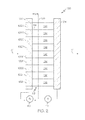
- one embodiment of the disclosed microplasma night vision device may include a photocathode 12, a transparent electrode 14 and a plurality of plasma cavities 16 positioned between the photocathode 12 and the transparent electrode 14.
- a voltage source 18 may apply a voltage V across the photocathode 12 and the transparent electrode 14.
- the photocathode 12 may be any material or structure that emits electrons in response to incident electromagnetic radiation (arrow A ) pursuant to the photoelectric effect and/or any material or structure that generates free electrons due to the photovoltaic effect.
- the photocathode 12 may emit/generate electrons in response to incident visible light.
- the photocathode 12 may emit/generate electrons in response to incident infrared light.
- the photocathode 12 may emit/generate electrons in response to both visible and infrared light. Therefore, the photocathode 12 may act as the electron source of the disclosed microplasma night vision device 10.
- the photocathode 12 may include a semiconductor material.
- the semiconductor material used in (or as) the photocathode 12 may include a p-n junction.
- the semiconductor material used in (or as) the photocathode 12 may include an intrinsic region between a p-type semiconductor and an n-type semiconductor.
- the semiconductor material used in (or as) the photocathode 12 may be a III-V compound semiconductor.
- suitable semiconductor materials that may be used in (or as) the photocathode 12 include, but are not limited to, silicon (Si), gallium arsenide (GaAs), indium gallium arsenide (InGaAs), gallium antimonide (GaSb), mercury cadmium telluride (HgCdTe), and indium antimonide (InSb). It is also contemplated that semiconductor composites may be used in (or as) the photocathode 12.
- the type of semiconductor material selected for use in (or as) the photocathode 12, particularly the band gap of the selected semiconductor material, may dictate the portion of the electromagnetic spectrum to which the disclosed microplasma night vision device 10 may be sensitive.
- a first transparent substrate may be layered over the outer surface 20 of the photocathode 12.
- the first transparent substrate may be a layer of glass, polymer or the like, and may structurally reinforce the disclosed microplasma night vision device 10.
- a second transparent electrode may optionally be positioned between the optional first transparent substrate and the photocathode 12 to enhance electrical conductivity proximate the photocathode 12.
- An objective lens (not shown) may optionally be included to collect and focus light onto the photocathode 12.
- the transparent electrode 14 may be spaced a distance D from the photocathode 12, and may be generally parallel with the photocathode 12.
- the distance D may be dictated by, among other things, the size, composition and configuration of the plasma cavities 16 between the transparent electrode 14 and the photocathode 12.
- the transparent electrode 14 may be generally electrically conductive.
- the transparent electrode 14 may have an electrical conductivity of at least 100 S/cm, such as at least 1000 S/cm or at least 10,000 S/cm.
- the transparent electrode 14 may be generally optically transparent to the light being observed by the microplasma night vision device 10.
- the transparent electrode 14 may have a transmittance of at least 50 percent, such as at least 75 percent or at least 90 percent.
- the transparent electrode 14 may be a thin-film, transparent conducting oxide.
- transparent conducting oxides suitable for use as the transparent electrode 14 include, but are not limited to, indium tin oxide (ITO), aluminum-doped zinc oxide, and fluorine-doped tin oxide.
- a second transparent substrate may be layered over the outer surface 22 of the transparent electrode 14.
- the second transparent substrate may be a layer of glass, polymer or the like, and may structurally reinforce the disclosed microplasma night vision device 10.
- each plasma cavity 16 may be arranged in parallel between the photocathode 12 and the transparent electrode 14. Therefore, each plasma cavity 16 may include a first end 24 electrically coupled to the photocathode 12 and a second end 26 electrically coupled to the transparent electrode 14.
- the plasma cavities 16 may be arranged in an array having a plurality of rows and column. Each plasma cavity 16 of the array may correspond to a pixel (or sub-pixel) of an image. Therefore, the array of plasma cavities 16 may form an image upon plasma ignition.
- Each plasma cavity 16 may house an ionizable gas.
- suitable ionizable gases include, but are not limited to, helium, neon, argon and other noble gases, and combinations thereof.
- the ionizable gas may be in admixture with a carrier gas, such as nitrogen.
- the voltage source 18 may apply a voltage V between the photocathode 12 and the transparent electrode 14.
- the applied voltage V may be less than, but proximate, the threshold voltage necessary to ionize the ionizable gas and ignite a plasma (e.g., a microplasma) within the plasma cavities 16.
- the threshold voltage may depend upon various factors, such as the size and shape of the plasma cavities 16 and the composition of the ionizable gas.
- the applied voltage V may be at least 70 percent of the threshold voltage, such as at least 80 percent, at least 90 percent, or at least 95 percent.
- the intensity of the plasmas formed within the plasma cavities 16 may depend on the number of electrons injected into the respective plasma cavities 16, which may be a function of the number of incoming photons (arrow A ).
- the intensity of the plasmas formed within the plasma cavities 16 may also depend on, among other things, the composition of the ionizable gas (which may also affect plasma color), the gas pressure, and the applied voltage V .
- the voltage V applied by the voltage source 18 may be at or above the threshold voltage necessary to ionize the ionizable gas within the plasma cavities 16. Therefore, incident photons (arrow A ) may cause electron emission into the plasma cavities 16, which may in turn alter the intensity of the plasma that is viewable as visible light (arrow B ) through the transparent electrode 14.
- FIG. 2 another embodiment of the disclosed microplasma night vision device, generally designated 100, may include a photocathode 102, a transparent electrode 104, a plurality of plasma cavities 106 and an accelerating grid 108.
- a first voltage source 110 may apply a first voltage V 1 between the photocathode 102 and the accelerating grid 108 and a second voltage source 112 may apply a second voltage V 2 between the accelerating grid 108 and the transparent electrode 104.
- the photocathode 102, the transparent electrode 104 and the plasma cavities 106 of the microplasma night vision device 100 may be configured as described above in connection with the microplasma night vision device 10.
- the photocathode 102 may be segmented into a plurality of photocathode segments 102A-102I. Each photocathode segment 102A-102I may be associated with a corresponding plasma cavity 106.
- the microplasma night vision device 100 may be constructed and operated in substantially the same way as the microplasma night vision device 10 discussed above. However, as is described in greater detail below, the addition of the accelerating grid 108 may facilitate field emission of electrons from the photocathode 102.
- the accelerating grid 108 may be positioned between the photocathode 102 and the transparent electrode 104, and may be spaced a distance S from the photocathode 102.
- the distance S between the photocathode 102 and the accelerating grid 108 may range from about 0 to about 50 percent of the distance D ( Fig. 1 ) between the photocathode 102 and the transparent electrode, such as from about 5 to about 25 percent of the distance D.
- the first voltage source 110 may apply a first voltage V 1 between the photocathode 102 (negative) and the accelerating grid 108 (positive).
- the first voltage V 1 may establish an electric field. Therefore, when the photocathode 102 is illuminated (arrow A' ), the electric field may induce field emission of electrons from the inner surface 114 of the photocathode 102, and may accelerate the electrons into the plasma cavities 106.
- the second voltage source 112 may apply a second voltage V 2 between the accelerating grid 108 and the transparent electrode 104.
- the second voltage V 2 may be less than, but proximate, the threshold voltage necessary to ionize the ionizable gas and ignite a plasma (e.g., a micro-plasma) within the plasma cavities 106.
- An AC voltage may optionally be used as the second voltage V 2 to inhibit erosion on the transparent electrode 104.
- the field emitted electrons accelerated into the plasma cavities 106 may ignite plasmas within the plasma cavities 106, thereby emitting visible light (arrow B') through the transparent electrode 104.
- the magnitude of the first voltage V 1 may be selected such that plasma ignition does not occur in the gap 116 between the photocathode 102 and the accelerating grid 108, but rather only occurs between the accelerating grid 108 and the transparent electrode 104.
- a method for sensing and amplifying incident photons.
- the method 200 may be used in a variety of applications, including but not limited to, night vision (visible and near infrared) and thermal imaging (infrared).
- the method 200 may begin at Block 202 with the step of providing a plurality of plasma cavities.
- the plasma cavities may be arranged in parallel between a photocathode and a transparent electrode.
- Each plasma cavity may house an ionizable gas (or mixture of ionizable gases).
- a voltage may be applied across the plasma cavities.
- the applied voltage may be less (e.g., just less) than the threshold voltage necessary to ionize the ionizable gas and ignite a plasma within the plasma cavities.
- the incident photons may be transduced to electrons.
- the step of transducing the incident photons to electrons may be performed by a photocathode.
- An optional accelerating grid may effect field emission of the electrons from the photocathode.
- the electrons may be introduced to the plasma cavities.
- the electrical energy within the plasma cavities may be sufficient to ignite plasmas within the plasma cavities, thereby outputting visible light (i.e., output photons).
- the disclosed method 200 employs a biasing voltage to generate microplasmas that output photons in response to incident photons, thereby effectively amplifying the incident photons.
- the disclosed microplasma night vision devices and methods generate visible plasmas in response to incident photons and, therefore, function as significantly powerful photon amplifiers.
- the photocathode material e.g., using advanced semiconductor materials
- engineering device topology and plasma ignition parameters it may be possible to achieve photon amplification ratios that are at least about 1 to 2 orders of magnitude higher than may be achieved using current night vision technology, such as Gen III night vision.
Landscapes
- Image-Pickup Tubes, Image-Amplification Tubes, And Storage Tubes (AREA)
- Gas-Filled Discharge Tubes (AREA)
- Photometry And Measurement Of Optical Pulse Characteristics (AREA)
- Transforming Light Signals Into Electric Signals (AREA)
Abstract
Description
- This application relates to light sensing and amplification and, more particularly, to night vision apparatus and methods.
- Night vision imaging is currently achieved by collecting and amplifying light. In one approach, ambient visible light (e.g., moonlight, starlight, plant luminescence and the like) is collected, converted to electrons, amplified and then converted to a visible image. In another approach, commonly referred to as thermal imaging, infrared photons emitted by an object that is warmer than the ambient environment (e.g., a living organism or a vehicle engine) are captured, such as with a charge-coupled device image sensor, and the image is then processed, amplified, and then displayed as a visible image.
- A typical ambient light-collecting night vision device includes an objective lens that collects light that may not be readily visible with the naked eye, and focuses the collected light onto an image intensifier. The image intensifier includes a photocathode that absorbs the collected light and converts it to electrons. A microchannel plate is often used to further amplify the electronic signal. The amplified electronic signal is then drawn toward, and strikes, a phosphor screen, thereby causing the screen to emit visible light. Since the phosphor screen emits visible light in exactly the same pattern and contrast as collected by the objective lens, an image is created on the phosphor screen that closely corresponds to the scene observed by the objective lens. The green image formed on the phosphor screen has become characteristic of night vision devices.
- Advances in night vision technology have brought about significant improvements in amplification. For example, so-called "Gen III" night vision devices have electron amplification ratios ranging from 30,000 to 50,000 and photon amplification ratios (i.e., photons out divided by photons in) of about 20 to 25. However, such night vision devices are relatively expensive and do not readily scale into large formats.
- Accordingly, those skilled in the art continue with research and development efforts in the field of night vision.
- In one embodiment, the disclosed photon sensing device may include a photocathode, a transparent electrode opposed from the photocathode, and a plasma chamber positioned between the photocathode and the transparent electrode, wherein the plasma chamber houses an ionizable gas.
- In another embodiment, the disclosed photon sensing device may include a photocathode, a transparent electrode opposed from the photocathode, a plasma chamber positioned between the photocathode and the transparent electrode, wherein the plasma chamber houses an ionizable gas, and a voltage source, wherein the voltage source applies a voltage across the plasma chamber. The applied voltage may be less than a threshold voltage required to ionize the ionizable gas.
- In another embodiment, the disclosed photon sensing device may include a photocathode, a transparent electrode opposed from the photocathode, a plurality of plasma chambers arranged in parallel between the photocathode and the transparent electrode, wherein each plasma chamber houses an ionizable gas, and a voltage source that applies a voltage across the plasma chambers. The applied voltage may be less than a threshold voltage required to ionize the ionizable gas within the plasma chambers.
- In yet another embodiment, also disclosed is a method for sensing incident photons. The method may include the steps of (1) providing a plasma cavity housing an ionizable gas, (2) applying a voltage across the plasma cavity, the applied voltage being less than a threshold voltage required to ionize the ionizable gas, (3) transducing the incident photons to electrons, and (4) introducing the electrons to the plasma cavity.
- Other embodiments of the disclosed microplasma night vision device and method will become apparent from the following detailed description, the accompanying drawings and the appended claims.
-
-
Fig. 1 is a schematic side elevational view, in section, of one embodiment of the disclosed microplasma night vision device; -
Fig. 2 is a schematic side elevational view, in section, of another embodiment of the disclosed microplasma night vision device; and -
Fig. 3 is a flow chart depicting one embodiment of the disclosed method for amplifying incident photons. - Disclosed are various photon sensing and amplifying devices and methods. While the disclosed photon sensing devices and methods are presented in the night vision and thermal imaging context (e.g., for use in goggles), various alternative applications, such as imaging, analysis and radiation detection, are also contemplated and will not result in a departure from the scope of the present disclosure.
- Referring to
Fig. 1 , one embodiment of the disclosed microplasma night vision device, generally designated 10, may include aphotocathode 12, atransparent electrode 14 and a plurality ofplasma cavities 16 positioned between thephotocathode 12 and thetransparent electrode 14. A voltage source 18 may apply a voltage V across thephotocathode 12 and thetransparent electrode 14. - The
photocathode 12 may be any material or structure that emits electrons in response to incident electromagnetic radiation (arrow A) pursuant to the photoelectric effect and/or any material or structure that generates free electrons due to the photovoltaic effect. In one particular construction, thephotocathode 12 may emit/generate electrons in response to incident visible light. In another particular construction, thephotocathode 12 may emit/generate electrons in response to incident infrared light. In yet another particular construction, thephotocathode 12 may emit/generate electrons in response to both visible and infrared light. Therefore, thephotocathode 12 may act as the electron source of the disclosed microplasmanight vision device 10. - The
photocathode 12 may include a semiconductor material. In one variation, the semiconductor material used in (or as) thephotocathode 12 may include a p-n junction. In another variation, the semiconductor material used in (or as) thephotocathode 12 may include an intrinsic region between a p-type semiconductor and an n-type semiconductor. In yet another variation, the semiconductor material used in (or as) thephotocathode 12 may be a III-V compound semiconductor. - Specific example of suitable semiconductor materials that may be used in (or as) the
photocathode 12 include, but are not limited to, silicon (Si), gallium arsenide (GaAs), indium gallium arsenide (InGaAs), gallium antimonide (GaSb), mercury cadmium telluride (HgCdTe), and indium antimonide (InSb). It is also contemplated that semiconductor composites may be used in (or as) thephotocathode 12. - At this point, those skilled in the art will appreciate that the type of semiconductor material selected for use in (or as) the
photocathode 12, particularly the band gap of the selected semiconductor material, may dictate the portion of the electromagnetic spectrum to which the disclosed microplasmanight vision device 10 may be sensitive. - Optionally, a first transparent substrate (not shown) may be layered over the
outer surface 20 of thephotocathode 12. For example, the first transparent substrate may be a layer of glass, polymer or the like, and may structurally reinforce the disclosed microplasmanight vision device 10. A second transparent electrode (not shown) may optionally be positioned between the optional first transparent substrate and thephotocathode 12 to enhance electrical conductivity proximate thephotocathode 12. An objective lens (not shown) may optionally be included to collect and focus light onto thephotocathode 12. - The
transparent electrode 14 may be spaced a distance D from thephotocathode 12, and may be generally parallel with thephotocathode 12. The distance D may be dictated by, among other things, the size, composition and configuration of theplasma cavities 16 between thetransparent electrode 14 and thephotocathode 12. - The
transparent electrode 14 may be generally electrically conductive. For example, thetransparent electrode 14 may have an electrical conductivity of at least 100 S/cm, such as at least 1000 S/cm or at least 10,000 S/cm. Furthermore, thetransparent electrode 14 may be generally optically transparent to the light being observed by the microplasmanight vision device 10. For example, thetransparent electrode 14 may have a transmittance of at least 50 percent, such as at least 75 percent or at least 90 percent. - In one particular construction, the
transparent electrode 14 may be a thin-film, transparent conducting oxide. Several examples of transparent conducting oxides suitable for use as thetransparent electrode 14 include, but are not limited to, indium tin oxide (ITO), aluminum-doped zinc oxide, and fluorine-doped tin oxide. - Optionally, a second transparent substrate (not shown) may be layered over the
outer surface 22 of thetransparent electrode 14. For example, the second transparent substrate may be a layer of glass, polymer or the like, and may structurally reinforce the disclosed microplasmanight vision device 10. - The
plasma cavities 16 may be arranged in parallel between thephotocathode 12 and thetransparent electrode 14. Therefore, eachplasma cavity 16 may include afirst end 24 electrically coupled to thephotocathode 12 and asecond end 26 electrically coupled to thetransparent electrode 14. - In one particular implementation, the
plasma cavities 16 may be arranged in an array having a plurality of rows and column. Eachplasma cavity 16 of the array may correspond to a pixel (or sub-pixel) of an image. Therefore, the array ofplasma cavities 16 may form an image upon plasma ignition. - Each
plasma cavity 16 may house an ionizable gas. Examples of suitable ionizable gases include, but are not limited to, helium, neon, argon and other noble gases, and combinations thereof. Optionally, the ionizable gas may be in admixture with a carrier gas, such as nitrogen. - The voltage source 18 may apply a voltage V between the
photocathode 12 and thetransparent electrode 14. The applied voltage V may be less than, but proximate, the threshold voltage necessary to ionize the ionizable gas and ignite a plasma (e.g., a microplasma) within theplasma cavities 16. The threshold voltage may depend upon various factors, such as the size and shape of theplasma cavities 16 and the composition of the ionizable gas. For example, the applied voltage V may be at least 70 percent of the threshold voltage, such as at least 80 percent, at least 90 percent, or at least 95 percent. - Thus, when the microplasma
night vision device 10 is exposed to electromagnetic energy above the band gap of thephotocathode 12, the incident photons (arrow A) may excite electron-hole pairs within thephotocathode 12. Upon separation of the electron-hole pairs, electrons may be directed into one or more of theplasma cavities 16, thereby igniting a transient plasma within therespective plasma cavities 16. The ignited plasma may persist so long as the flow of electrons persists, and may have a color and intensity. The ignited plasma may be viewed as visible light (arrow B) through thetransparent electrode 14. - At this point, those skilled in the art will appreciate that the intensity of the plasmas formed within the
plasma cavities 16 may depend on the number of electrons injected into therespective plasma cavities 16, which may be a function of the number of incoming photons (arrow A). The intensity of the plasmas formed within theplasma cavities 16 may also depend on, among other things, the composition of the ionizable gas (which may also affect plasma color), the gas pressure, and the applied voltage V. - In one contemplated alternative implementation, the voltage V applied by the voltage source 18 may be at or above the threshold voltage necessary to ionize the ionizable gas within the
plasma cavities 16. Therefore, incident photons (arrow A) may cause electron emission into theplasma cavities 16, which may in turn alter the intensity of the plasma that is viewable as visible light (arrow B) through thetransparent electrode 14. - Referring to
Fig. 2 , another embodiment of the disclosed microplasma night vision device, generally designated 100, may include aphotocathode 102, atransparent electrode 104, a plurality ofplasma cavities 106 and an acceleratinggrid 108. Afirst voltage source 110 may apply a first voltage V1 between thephotocathode 102 and the acceleratinggrid 108 and asecond voltage source 112 may apply a second voltage V2 between the acceleratinggrid 108 and thetransparent electrode 104. - The
photocathode 102, thetransparent electrode 104 and theplasma cavities 106 of the microplasmanight vision device 100 may be configured as described above in connection with the microplasmanight vision device 10. Optionally, thephotocathode 102 may be segmented into a plurality ofphotocathode segments 102A-102I. Eachphotocathode segment 102A-102I may be associated with acorresponding plasma cavity 106. - Thus, the microplasma
night vision device 100 may be constructed and operated in substantially the same way as the microplasmanight vision device 10 discussed above. However, as is described in greater detail below, the addition of the acceleratinggrid 108 may facilitate field emission of electrons from thephotocathode 102. - The accelerating
grid 108 may be positioned between thephotocathode 102 and thetransparent electrode 104, and may be spaced a distance S from thephotocathode 102. The distance S between thephotocathode 102 and the acceleratinggrid 108 may range from about 0 to about 50 percent of the distance D (Fig. 1 ) between thephotocathode 102 and the transparent electrode, such as from about 5 to about 25 percent of the distance D. - The
first voltage source 110 may apply a first voltage V1 between the photocathode 102 (negative) and the accelerating grid 108 (positive). The first voltage V1 may establish an electric field. Therefore, when thephotocathode 102 is illuminated (arrow A'), the electric field may induce field emission of electrons from theinner surface 114 of thephotocathode 102, and may accelerate the electrons into theplasma cavities 106. - The
second voltage source 112 may apply a second voltage V2 between the acceleratinggrid 108 and thetransparent electrode 104. The second voltage V2 may be less than, but proximate, the threshold voltage necessary to ionize the ionizable gas and ignite a plasma (e.g., a micro-plasma) within theplasma cavities 106. An AC voltage may optionally be used as the second voltage V2 to inhibit erosion on thetransparent electrode 104. - Thus, the field emitted electrons accelerated into the
plasma cavities 106 may ignite plasmas within theplasma cavities 106, thereby emitting visible light (arrow B') through thetransparent electrode 104. Optionally, the magnitude of the first voltage V1 may be selected such that plasma ignition does not occur in thegap 116 between thephotocathode 102 and the acceleratinggrid 108, but rather only occurs between the acceleratinggrid 108 and thetransparent electrode 104. - Referring to
Fig. 3 , also disclosed is a method, generally designated 200, for sensing and amplifying incident photons. Themethod 200 may be used in a variety of applications, including but not limited to, night vision (visible and near infrared) and thermal imaging (infrared). - The
method 200 may begin atBlock 202 with the step of providing a plurality of plasma cavities. The plasma cavities may be arranged in parallel between a photocathode and a transparent electrode. Each plasma cavity may house an ionizable gas (or mixture of ionizable gases). - At
Block 204, a voltage may be applied across the plasma cavities. The applied voltage may be less (e.g., just less) than the threshold voltage necessary to ionize the ionizable gas and ignite a plasma within the plasma cavities. - At
Block 206, the incident photons may be transduced to electrons. The step of transducing the incident photons to electrons may be performed by a photocathode. An optional accelerating grid may effect field emission of the electrons from the photocathode. - At
Block 208, the electrons may be introduced to the plasma cavities. Upon introducing the electrons to the plasma cavities, the electrical energy within the plasma cavities may be sufficient to ignite plasmas within the plasma cavities, thereby outputting visible light (i.e., output photons). - Thus, the disclosed
method 200 employs a biasing voltage to generate microplasmas that output photons in response to incident photons, thereby effectively amplifying the incident photons. - Accordingly, the disclosed microplasma night vision devices and methods generate visible plasmas in response to incident photons and, therefore, function as significantly powerful photon amplifiers. By carefully selecting the photocathode material (e.g., using advanced semiconductor materials), as well as engineering device topology and plasma ignition parameters, it may be possible to achieve photon amplification ratios that are at least about 1 to 2 orders of magnitude higher than may be achieved using current night vision technology, such as Gen III night vision.
- Although various embodiments of the disclosed microplasma night vision device and method have been shown and described, modifications may occur to those skilled in the art upon reading the specification. The present application includes such modifications and is limited only by the scope of the claims.
Claims (16)
- A photon sensing device comprising:a photocathode;a transparent electrode opposed from said photocathode; andat least one plasma chamber positioned between said photocathode and said transparent electrode, said at least one plasma chamber housing an ionizable gas.
- The photon sensing device of Claim 1 further comprising a voltage source, wherein said voltage source applies a voltage across said plasma chamber, said voltage being less than a threshold voltage required to ionize said ionizable gas.
- The photon sensing device of Claim 2 wherein said voltage is at least 90 percent of said threshold voltage.
- The photon sensing device of any one of Claims 1 to 3, wherein said photocathode is sensitive to at least one of visible light and infrared light.
- The photon sensing device of any one of Claims 1 to 4, wherein said photocathode comprises a semiconductor material, such as a semiconducting material selected from the group consisting of silicon, gallium arsenide, indium gallium arsenide, gallium antimonide, mercury cadmium telluride, indium antimonide, and combinations thereof.
- The photon sensing device of any one of Claims 1 to 5, wherein said transparent electrode comprises a transparent conducting oxide, such as a transparent conducting oxide selected from the group consisting of indium tin oxide, aluminum-doped zinc oxide, fluorine-doped tin oxide, and combinations thereof.
- The photon sensing device of any one of Claims 1 to 6 comprising a plurality of plasma chambers, wherein each plasma chamber of said plurality of plasma chambers houses said ionizable gas.
- The photon sensing device of any one of Claims 1 to 7, wherein said ionizable gas comprises a noble gas.
- The photon sensing device of any one of Claims 1 to 8, further comprising an accelerating grid positioned between said photocathode and said transparent electrode.
- The photon sensing device of Claim 9 wherein a first voltage source applies a first voltage between said photocathode and said accelerating grid.
- The photon sensing device of Claim 10 wherein a second voltage source applies a second voltage between said accelerating grid and said transparent electrode.
- The photon sensing device of Claim 7, or any one of Claims 8 to 11 when dependent upon Claim 7, wherein the plurality of plasma chambers are arranged in parallel between said photocathode and said transparent electrode.
- Goggles comprising the photon sensing device of any one of Claims 1 to 12.
- The goggles of Claim 13 further comprising an objective lens.
- A method for sensing incident photons comprising the steps of:providing a plasma cavity housing an ionizable gas;applying a voltage across said plasma cavity, said applied voltage being less than a threshold voltage required to ionize said ionizable gas;transducing said incident photons to electrons; andintroducing said electrons to said plasma cavity.
- The method of Claim 15 further comprising the step of accelerating said electrons into said plasma cavity.
Applications Claiming Priority (1)
| Application Number | Priority Date | Filing Date | Title |
|---|---|---|---|
| US13/558,012 US8872094B2 (en) | 2012-07-25 | 2012-07-25 | Microplasma night vision device |
Publications (3)
| Publication Number | Publication Date |
|---|---|
| EP2690644A2 true EP2690644A2 (en) | 2014-01-29 |
| EP2690644A3 EP2690644A3 (en) | 2017-08-16 |
| EP2690644B1 EP2690644B1 (en) | 2019-03-06 |
Family
ID=48877072
Family Applications (1)
| Application Number | Title | Priority Date | Filing Date |
|---|---|---|---|
| EP13177868.0A Not-in-force EP2690644B1 (en) | 2012-07-25 | 2013-07-24 | Microplasma night vision device |
Country Status (4)
| Country | Link |
|---|---|
| US (1) | US8872094B2 (en) |
| EP (1) | EP2690644B1 (en) |
| JP (1) | JP6355900B2 (en) |
| CN (1) | CN103578892B (en) |
Families Citing this family (1)
| Publication number | Priority date | Publication date | Assignee | Title |
|---|---|---|---|---|
| US9960005B2 (en) * | 2012-08-08 | 2018-05-01 | Massachusetts Institute Of Technology | Microplasma generation devices and associated systems and methods |
Family Cites Families (10)
| Publication number | Priority date | Publication date | Assignee | Title |
|---|---|---|---|---|
| US3213312A (en) * | 1963-05-22 | 1965-10-19 | Mc Graw Edison Co | Ultraviolet detector tube with a gas filling of hydrogen, helium and a noble gas |
| GB1455011A (en) * | 1973-05-21 | 1976-11-10 | Agfa Gevaert | Electrostatic imaging device and process using same |
| JPS5922351B2 (en) * | 1976-04-20 | 1984-05-25 | 松下電器産業株式会社 | Luminous screen |
| US4039830A (en) * | 1976-08-13 | 1977-08-02 | General Electric Company | Electrostatic x-ray image recording device with mesh-base photocathode photoelectron discriminator means |
| US5311010A (en) * | 1993-02-01 | 1994-05-10 | The United States Of America As Represented By The United States Department Of Energy | Buffer for a gamma-insensitive optical sensor with gas and a buffer assembly |
| US5942747A (en) * | 1997-07-28 | 1999-08-24 | Litton Systems, Inc. | Night vision device with voltage to photocathode having a rectified half-sine wave component |
| US6828730B2 (en) * | 2002-11-27 | 2004-12-07 | Board Of Trustees Of The University Of Illinois | Microdischarge photodetectors |
| CN1854761A (en) * | 2005-04-29 | 2006-11-01 | 中国科学院西安光学精密机械研究所 | Ultraviolet image intensifier |
| US7459684B2 (en) * | 2005-05-18 | 2008-12-02 | Lockheed Martin Corporation | Long-wavelength infra-red night vision goggles |
| US7804651B2 (en) * | 2008-11-25 | 2010-09-28 | Itt Manufacturing Enterprises, Inc. | Flat field eyepiece |
-
2012
- 2012-07-25 US US13/558,012 patent/US8872094B2/en not_active Expired - Fee Related
-
2013
- 2013-05-22 CN CN201310193963.3A patent/CN103578892B/en not_active Expired - Fee Related
- 2013-07-24 EP EP13177868.0A patent/EP2690644B1/en not_active Not-in-force
- 2013-07-24 JP JP2013153976A patent/JP6355900B2/en not_active Expired - Fee Related
Non-Patent Citations (1)
| Title |
|---|
| None |
Also Published As
| Publication number | Publication date |
|---|---|
| JP2014053292A (en) | 2014-03-20 |
| JP6355900B2 (en) | 2018-07-11 |
| US8872094B2 (en) | 2014-10-28 |
| CN103578892B (en) | 2017-10-03 |
| US20140027622A1 (en) | 2014-01-30 |
| CN103578892A (en) | 2014-02-12 |
| EP2690644A3 (en) | 2017-08-16 |
| EP2690644B1 (en) | 2019-03-06 |
Similar Documents
| Publication | Publication Date | Title |
|---|---|---|
| JP4639379B2 (en) | Detector for bipolar time-of-flight mass spectrometer | |
| WO2016187603A1 (en) | Photocathode including field emitter array on a silicon substrate with boron layer | |
| CN108092624A (en) | A kind of detection device and its detection method of the distribution of solar cell open-circuit voltage | |
| CN207197676U (en) | Solar blind ultraviolet single photon imaging system | |
| EP2761641A1 (en) | Bright source protection for low light imaging sensors | |
| EP3127138A1 (en) | Ultraviolet light detection | |
| US8872094B2 (en) | Microplasma night vision device | |
| US4870265A (en) | Position-sensitive radiation detector | |
| Zhao et al. | Study of a neutron-resistant p+-Si/n-ZnO photodetector with avalanching gain | |
| US6836059B2 (en) | Image intensifier and electron multiplier therefor | |
| CN102403048A (en) | AlZnO ultraviolet photocathode material and ultraviolet vacuum image intensifier | |
| Barbarino et al. | Proof of feasibility of the vacuum silicon photomultiplier tube (vsipmt) | |
| CN104505421B (en) | A kind of avalanche photodide with self-gravitation self-recovering function | |
| CN104505422B (en) | A kind of self-gravitation self- recoverage avalanche photodide | |
| US12009439B2 (en) | Photodiode and method for operating a photodiode | |
| RU141786U1 (en) | PHOTOELECTRONIC PROXIMITY TYPE WITH PHOTOCATHODE BASED ON HETEROSTRUCTURE А3В5 | |
| RU141372U1 (en) | HIGH VOLTAGE HYBRID PHOTOSENSITIVE INSTRUMENT FOR REGISTRATION OF RADIATION OF LOW INTENSITY | |
| JP5778179B2 (en) | Infrared external photoemission detector | |
| Kurt et al. | The observations of the IR sensitivity enhancement, negative differential resistance and hysteresis in a microelectronic gas discharge device with GaP | |
| Zhang et al. | The simulation of EBAPS based on new passivation layer structure | |
| Liu et al. | Function and its significance of screen luminous efficiency curve | |
| CN103887125A (en) | Transmission-type GaAs photoelectric cathode based on gradient doping nanometer ZnO thin film field transmission assistance | |
| Smith et al. | Development of hybrid photodetectors using single-crystal III–V photocathodes | |
| Rui et al. | Study on measurement method of luminous intensity based on the third generation low light level image intensifier | |
| Schomaker | Performance of the hybrid photomultiplier tube (HPMT) |
Legal Events
| Date | Code | Title | Description |
|---|---|---|---|
| PUAI | Public reference made under article 153(3) epc to a published international application that has entered the european phase |
Free format text: ORIGINAL CODE: 0009012 |
|
| AK | Designated contracting states |
Kind code of ref document: A2 Designated state(s): AL AT BE BG CH CY CZ DE DK EE ES FI FR GB GR HR HU IE IS IT LI LT LU LV MC MK MT NL NO PL PT RO RS SE SI SK SM TR |
|
| AX | Request for extension of the european patent |
Extension state: BA ME |
|
| PUAL | Search report despatched |
Free format text: ORIGINAL CODE: 0009013 |
|
| AK | Designated contracting states |
Kind code of ref document: A3 Designated state(s): AL AT BE BG CH CY CZ DE DK EE ES FI FR GB GR HR HU IE IS IT LI LT LU LV MC MK MT NL NO PL PT RO RS SE SI SK SM TR |
|
| AX | Request for extension of the european patent |
Extension state: BA ME |
|
| RIC1 | Information provided on ipc code assigned before grant |
Ipc: H01J 47/02 20060101ALI20170707BHEP Ipc: H01J 31/50 20060101AFI20170707BHEP Ipc: G02B 23/12 20060101ALI20170707BHEP |
|
| STAA | Information on the status of an ep patent application or granted ep patent |
Free format text: STATUS: REQUEST FOR EXAMINATION WAS MADE |
|
| 17P | Request for examination filed |
Effective date: 20180214 |
|
| RBV | Designated contracting states (corrected) |
Designated state(s): AL AT BE BG CH CY CZ DE DK EE ES FI FR GB GR HR HU IE IS IT LI LT LU LV MC MK MT NL NO PL PT RO RS SE SI SK SM TR |
|
| GRAP | Despatch of communication of intention to grant a patent |
Free format text: ORIGINAL CODE: EPIDOSNIGR1 |
|
| STAA | Information on the status of an ep patent application or granted ep patent |
Free format text: STATUS: GRANT OF PATENT IS INTENDED |
|
| INTG | Intention to grant announced |
Effective date: 20180417 |
|
| GRAJ | Information related to disapproval of communication of intention to grant by the applicant or resumption of examination proceedings by the epo deleted |
Free format text: ORIGINAL CODE: EPIDOSDIGR1 |
|
| STAA | Information on the status of an ep patent application or granted ep patent |
Free format text: STATUS: REQUEST FOR EXAMINATION WAS MADE |
|
| GRAP | Despatch of communication of intention to grant a patent |
Free format text: ORIGINAL CODE: EPIDOSNIGR1 |
|
| STAA | Information on the status of an ep patent application or granted ep patent |
Free format text: STATUS: GRANT OF PATENT IS INTENDED |
|
| INTC | Intention to grant announced (deleted) | ||
| INTG | Intention to grant announced |
Effective date: 20180912 |
|
| GRAS | Grant fee paid |
Free format text: ORIGINAL CODE: EPIDOSNIGR3 |
|
| GRAA | (expected) grant |
Free format text: ORIGINAL CODE: 0009210 |
|
| STAA | Information on the status of an ep patent application or granted ep patent |
Free format text: STATUS: THE PATENT HAS BEEN GRANTED |
|
| AK | Designated contracting states |
Kind code of ref document: B1 Designated state(s): AL AT BE BG CH CY CZ DE DK EE ES FI FR GB GR HR HU IE IS IT LI LT LU LV MC MK MT NL NO PL PT RO RS SE SI SK SM TR |
|
| REG | Reference to a national code |
Ref country code: GB Ref legal event code: FG4D |
|
| REG | Reference to a national code |
Ref country code: CH Ref legal event code: EP Ref country code: AT Ref legal event code: REF Ref document number: 1105676 Country of ref document: AT Kind code of ref document: T Effective date: 20190315 |
|
| REG | Reference to a national code |
Ref country code: DE Ref legal event code: R096 Ref document number: 602013051720 Country of ref document: DE |
|
| REG | Reference to a national code |
Ref country code: IE Ref legal event code: FG4D |
|
| REG | Reference to a national code |
Ref country code: NL Ref legal event code: MP Effective date: 20190306 |
|
| REG | Reference to a national code |
Ref country code: LT Ref legal event code: MG4D |
|
| PG25 | Lapsed in a contracting state [announced via postgrant information from national office to epo] |
Ref country code: NO Free format text: LAPSE BECAUSE OF FAILURE TO SUBMIT A TRANSLATION OF THE DESCRIPTION OR TO PAY THE FEE WITHIN THE PRESCRIBED TIME-LIMIT Effective date: 20190606 Ref country code: LT Free format text: LAPSE BECAUSE OF FAILURE TO SUBMIT A TRANSLATION OF THE DESCRIPTION OR TO PAY THE FEE WITHIN THE PRESCRIBED TIME-LIMIT Effective date: 20190306 Ref country code: SE Free format text: LAPSE BECAUSE OF FAILURE TO SUBMIT A TRANSLATION OF THE DESCRIPTION OR TO PAY THE FEE WITHIN THE PRESCRIBED TIME-LIMIT Effective date: 20190306 Ref country code: FI Free format text: LAPSE BECAUSE OF FAILURE TO SUBMIT A TRANSLATION OF THE DESCRIPTION OR TO PAY THE FEE WITHIN THE PRESCRIBED TIME-LIMIT Effective date: 20190306 |
|
| PG25 | Lapsed in a contracting state [announced via postgrant information from national office to epo] |
Ref country code: LV Free format text: LAPSE BECAUSE OF FAILURE TO SUBMIT A TRANSLATION OF THE DESCRIPTION OR TO PAY THE FEE WITHIN THE PRESCRIBED TIME-LIMIT Effective date: 20190306 Ref country code: BG Free format text: LAPSE BECAUSE OF FAILURE TO SUBMIT A TRANSLATION OF THE DESCRIPTION OR TO PAY THE FEE WITHIN THE PRESCRIBED TIME-LIMIT Effective date: 20190606 Ref country code: RS Free format text: LAPSE BECAUSE OF FAILURE TO SUBMIT A TRANSLATION OF THE DESCRIPTION OR TO PAY THE FEE WITHIN THE PRESCRIBED TIME-LIMIT Effective date: 20190306 Ref country code: GR Free format text: LAPSE BECAUSE OF FAILURE TO SUBMIT A TRANSLATION OF THE DESCRIPTION OR TO PAY THE FEE WITHIN THE PRESCRIBED TIME-LIMIT Effective date: 20190607 Ref country code: NL Free format text: LAPSE BECAUSE OF FAILURE TO SUBMIT A TRANSLATION OF THE DESCRIPTION OR TO PAY THE FEE WITHIN THE PRESCRIBED TIME-LIMIT Effective date: 20190306 Ref country code: HR Free format text: LAPSE BECAUSE OF FAILURE TO SUBMIT A TRANSLATION OF THE DESCRIPTION OR TO PAY THE FEE WITHIN THE PRESCRIBED TIME-LIMIT Effective date: 20190306 |
|
| REG | Reference to a national code |
Ref country code: AT Ref legal event code: MK05 Ref document number: 1105676 Country of ref document: AT Kind code of ref document: T Effective date: 20190306 |
|
| PG25 | Lapsed in a contracting state [announced via postgrant information from national office to epo] |
Ref country code: PT Free format text: LAPSE BECAUSE OF FAILURE TO SUBMIT A TRANSLATION OF THE DESCRIPTION OR TO PAY THE FEE WITHIN THE PRESCRIBED TIME-LIMIT Effective date: 20190706 Ref country code: AL Free format text: LAPSE BECAUSE OF FAILURE TO SUBMIT A TRANSLATION OF THE DESCRIPTION OR TO PAY THE FEE WITHIN THE PRESCRIBED TIME-LIMIT Effective date: 20190306 Ref country code: ES Free format text: LAPSE BECAUSE OF FAILURE TO SUBMIT A TRANSLATION OF THE DESCRIPTION OR TO PAY THE FEE WITHIN THE PRESCRIBED TIME-LIMIT Effective date: 20190306 Ref country code: SK Free format text: LAPSE BECAUSE OF FAILURE TO SUBMIT A TRANSLATION OF THE DESCRIPTION OR TO PAY THE FEE WITHIN THE PRESCRIBED TIME-LIMIT Effective date: 20190306 Ref country code: IT Free format text: LAPSE BECAUSE OF FAILURE TO SUBMIT A TRANSLATION OF THE DESCRIPTION OR TO PAY THE FEE WITHIN THE PRESCRIBED TIME-LIMIT Effective date: 20190306 Ref country code: EE Free format text: LAPSE BECAUSE OF FAILURE TO SUBMIT A TRANSLATION OF THE DESCRIPTION OR TO PAY THE FEE WITHIN THE PRESCRIBED TIME-LIMIT Effective date: 20190306 Ref country code: CZ Free format text: LAPSE BECAUSE OF FAILURE TO SUBMIT A TRANSLATION OF THE DESCRIPTION OR TO PAY THE FEE WITHIN THE PRESCRIBED TIME-LIMIT Effective date: 20190306 Ref country code: RO Free format text: LAPSE BECAUSE OF FAILURE TO SUBMIT A TRANSLATION OF THE DESCRIPTION OR TO PAY THE FEE WITHIN THE PRESCRIBED TIME-LIMIT Effective date: 20190306 |
|
| PG25 | Lapsed in a contracting state [announced via postgrant information from national office to epo] |
Ref country code: PL Free format text: LAPSE BECAUSE OF FAILURE TO SUBMIT A TRANSLATION OF THE DESCRIPTION OR TO PAY THE FEE WITHIN THE PRESCRIBED TIME-LIMIT Effective date: 20190306 Ref country code: SM Free format text: LAPSE BECAUSE OF FAILURE TO SUBMIT A TRANSLATION OF THE DESCRIPTION OR TO PAY THE FEE WITHIN THE PRESCRIBED TIME-LIMIT Effective date: 20190306 |
|
| REG | Reference to a national code |
Ref country code: DE Ref legal event code: R097 Ref document number: 602013051720 Country of ref document: DE |
|
| PG25 | Lapsed in a contracting state [announced via postgrant information from national office to epo] |
Ref country code: IS Free format text: LAPSE BECAUSE OF FAILURE TO SUBMIT A TRANSLATION OF THE DESCRIPTION OR TO PAY THE FEE WITHIN THE PRESCRIBED TIME-LIMIT Effective date: 20190706 Ref country code: AT Free format text: LAPSE BECAUSE OF FAILURE TO SUBMIT A TRANSLATION OF THE DESCRIPTION OR TO PAY THE FEE WITHIN THE PRESCRIBED TIME-LIMIT Effective date: 20190306 |
|
| PLBE | No opposition filed within time limit |
Free format text: ORIGINAL CODE: 0009261 |
|
| STAA | Information on the status of an ep patent application or granted ep patent |
Free format text: STATUS: NO OPPOSITION FILED WITHIN TIME LIMIT |
|
| REG | Reference to a national code |
Ref country code: DE Ref legal event code: R082 Ref document number: 602013051720 Country of ref document: DE Representative=s name: MAIER, LL.M., MICHAEL C., DE Ref country code: DE Ref legal event code: R082 Ref document number: 602013051720 Country of ref document: DE Representative=s name: BOULT WADE TENNANT LLP, DE |
|
| PG25 | Lapsed in a contracting state [announced via postgrant information from national office to epo] |
Ref country code: DK Free format text: LAPSE BECAUSE OF FAILURE TO SUBMIT A TRANSLATION OF THE DESCRIPTION OR TO PAY THE FEE WITHIN THE PRESCRIBED TIME-LIMIT Effective date: 20190306 |
|
| 26N | No opposition filed |
Effective date: 20191209 |
|
| REG | Reference to a national code |
Ref country code: DE Ref legal event code: R082 Ref document number: 602013051720 Country of ref document: DE Representative=s name: BOULT WADE TENNANT LLP, DE |
|
| PG25 | Lapsed in a contracting state [announced via postgrant information from national office to epo] |
Ref country code: MC Free format text: LAPSE BECAUSE OF FAILURE TO SUBMIT A TRANSLATION OF THE DESCRIPTION OR TO PAY THE FEE WITHIN THE PRESCRIBED TIME-LIMIT Effective date: 20190306 Ref country code: SI Free format text: LAPSE BECAUSE OF FAILURE TO SUBMIT A TRANSLATION OF THE DESCRIPTION OR TO PAY THE FEE WITHIN THE PRESCRIBED TIME-LIMIT Effective date: 20190306 |
|
| REG | Reference to a national code |
Ref country code: CH Ref legal event code: PL |
|
| PG25 | Lapsed in a contracting state [announced via postgrant information from national office to epo] |
Ref country code: TR Free format text: LAPSE BECAUSE OF FAILURE TO SUBMIT A TRANSLATION OF THE DESCRIPTION OR TO PAY THE FEE WITHIN THE PRESCRIBED TIME-LIMIT Effective date: 20190306 |
|
| REG | Reference to a national code |
Ref country code: BE Ref legal event code: MM Effective date: 20190731 |
|
| PG25 | Lapsed in a contracting state [announced via postgrant information from national office to epo] |
Ref country code: BE Free format text: LAPSE BECAUSE OF NON-PAYMENT OF DUE FEES Effective date: 20190731 Ref country code: LU Free format text: LAPSE BECAUSE OF NON-PAYMENT OF DUE FEES Effective date: 20190724 Ref country code: LI Free format text: LAPSE BECAUSE OF NON-PAYMENT OF DUE FEES Effective date: 20190731 Ref country code: CH Free format text: LAPSE BECAUSE OF NON-PAYMENT OF DUE FEES Effective date: 20190731 |
|
| PG25 | Lapsed in a contracting state [announced via postgrant information from national office to epo] |
Ref country code: IE Free format text: LAPSE BECAUSE OF NON-PAYMENT OF DUE FEES Effective date: 20190724 |
|
| PG25 | Lapsed in a contracting state [announced via postgrant information from national office to epo] |
Ref country code: CY Free format text: LAPSE BECAUSE OF FAILURE TO SUBMIT A TRANSLATION OF THE DESCRIPTION OR TO PAY THE FEE WITHIN THE PRESCRIBED TIME-LIMIT Effective date: 20190306 |
|
| PG25 | Lapsed in a contracting state [announced via postgrant information from national office to epo] |
Ref country code: HU Free format text: LAPSE BECAUSE OF FAILURE TO SUBMIT A TRANSLATION OF THE DESCRIPTION OR TO PAY THE FEE WITHIN THE PRESCRIBED TIME-LIMIT; INVALID AB INITIO Effective date: 20130724 Ref country code: MT Free format text: LAPSE BECAUSE OF FAILURE TO SUBMIT A TRANSLATION OF THE DESCRIPTION OR TO PAY THE FEE WITHIN THE PRESCRIBED TIME-LIMIT Effective date: 20190306 |
|
| PGFP | Annual fee paid to national office [announced via postgrant information from national office to epo] |
Ref country code: FR Payment date: 20210726 Year of fee payment: 9 |
|
| PGFP | Annual fee paid to national office [announced via postgrant information from national office to epo] |
Ref country code: DE Payment date: 20210728 Year of fee payment: 9 Ref country code: GB Payment date: 20210727 Year of fee payment: 9 |
|
| PG25 | Lapsed in a contracting state [announced via postgrant information from national office to epo] |
Ref country code: MK Free format text: LAPSE BECAUSE OF FAILURE TO SUBMIT A TRANSLATION OF THE DESCRIPTION OR TO PAY THE FEE WITHIN THE PRESCRIBED TIME-LIMIT Effective date: 20190306 |
|
| REG | Reference to a national code |
Ref country code: DE Ref legal event code: R119 Ref document number: 602013051720 Country of ref document: DE |
|
| GBPC | Gb: european patent ceased through non-payment of renewal fee |
Effective date: 20220724 |
|
| PG25 | Lapsed in a contracting state [announced via postgrant information from national office to epo] |
Ref country code: FR Free format text: LAPSE BECAUSE OF NON-PAYMENT OF DUE FEES Effective date: 20220731 |
|
| PG25 | Lapsed in a contracting state [announced via postgrant information from national office to epo] |
Ref country code: GB Free format text: LAPSE BECAUSE OF NON-PAYMENT OF DUE FEES Effective date: 20220724 Ref country code: DE Free format text: LAPSE BECAUSE OF NON-PAYMENT OF DUE FEES Effective date: 20230201 |