EP2687899B1 - Method and system for manufacturing a roll of optical film laminate - Google Patents
Method and system for manufacturing a roll of optical film laminate Download PDFInfo
- Publication number
- EP2687899B1 EP2687899B1 EP13189209.3A EP13189209A EP2687899B1 EP 2687899 B1 EP2687899 B1 EP 2687899B1 EP 13189209 A EP13189209 A EP 13189209A EP 2687899 B1 EP2687899 B1 EP 2687899B1
- Authority
- EP
- European Patent Office
- Prior art keywords
- film
- polarizing
- optical film
- optical
- polarizing composite
- Prior art date
- Legal status (The legal status is an assumption and is not a legal conclusion. Google has not performed a legal analysis and makes no representation as to the accuracy of the status listed.)
- Not-in-force
Links
Images


Classifications
-
- G—PHYSICS
- G02—OPTICS
- G02F—OPTICAL DEVICES OR ARRANGEMENTS FOR THE CONTROL OF LIGHT BY MODIFICATION OF THE OPTICAL PROPERTIES OF THE MEDIA OF THE ELEMENTS INVOLVED THEREIN; NON-LINEAR OPTICS; FREQUENCY-CHANGING OF LIGHT; OPTICAL LOGIC ELEMENTS; OPTICAL ANALOGUE/DIGITAL CONVERTERS
- G02F1/00—Devices or arrangements for the control of the intensity, colour, phase, polarisation or direction of light arriving from an independent light source, e.g. switching, gating or modulating; Non-linear optics
- G02F1/01—Devices or arrangements for the control of the intensity, colour, phase, polarisation or direction of light arriving from an independent light source, e.g. switching, gating or modulating; Non-linear optics for the control of the intensity, phase, polarisation or colour
- G02F1/13—Devices or arrangements for the control of the intensity, colour, phase, polarisation or direction of light arriving from an independent light source, e.g. switching, gating or modulating; Non-linear optics for the control of the intensity, phase, polarisation or colour based on liquid crystals, e.g. single liquid crystal display cells
- G02F1/133—Constructional arrangements; Operation of liquid crystal cells; Circuit arrangements
- G02F1/1333—Constructional arrangements; Manufacturing methods
- G02F1/1335—Structural association of cells with optical devices, e.g. polarisers or reflectors
- G02F1/133528—Polarisers
-
- B—PERFORMING OPERATIONS; TRANSPORTING
- B32—LAYERED PRODUCTS
- B32B—LAYERED PRODUCTS, i.e. PRODUCTS BUILT-UP OF STRATA OF FLAT OR NON-FLAT, e.g. CELLULAR OR HONEYCOMB, FORM
- B32B38/00—Ancillary operations in connection with laminating processes
- B32B38/18—Handling of layers or the laminate
- B32B38/1825—Handling of layers or the laminate characterised by the control or constructional features of devices for tensioning, stretching or registration
- B32B38/1833—Positioning, e.g. registration or centering
- B32B38/1841—Positioning, e.g. registration or centering during laying up
-
- B—PERFORMING OPERATIONS; TRANSPORTING
- B32—LAYERED PRODUCTS
- B32B—LAYERED PRODUCTS, i.e. PRODUCTS BUILT-UP OF STRATA OF FLAT OR NON-FLAT, e.g. CELLULAR OR HONEYCOMB, FORM
- B32B41/00—Arrangements for controlling or monitoring lamination processes; Safety arrangements
-
- G—PHYSICS
- G02—OPTICS
- G02F—OPTICAL DEVICES OR ARRANGEMENTS FOR THE CONTROL OF LIGHT BY MODIFICATION OF THE OPTICAL PROPERTIES OF THE MEDIA OF THE ELEMENTS INVOLVED THEREIN; NON-LINEAR OPTICS; FREQUENCY-CHANGING OF LIGHT; OPTICAL LOGIC ELEMENTS; OPTICAL ANALOGUE/DIGITAL CONVERTERS
- G02F1/00—Devices or arrangements for the control of the intensity, colour, phase, polarisation or direction of light arriving from an independent light source, e.g. switching, gating or modulating; Non-linear optics
- G02F1/01—Devices or arrangements for the control of the intensity, colour, phase, polarisation or direction of light arriving from an independent light source, e.g. switching, gating or modulating; Non-linear optics for the control of the intensity, phase, polarisation or colour
- G02F1/13—Devices or arrangements for the control of the intensity, colour, phase, polarisation or direction of light arriving from an independent light source, e.g. switching, gating or modulating; Non-linear optics for the control of the intensity, phase, polarisation or colour based on liquid crystals, e.g. single liquid crystal display cells
- G02F1/1303—Apparatus specially adapted to the manufacture of LCDs
-
- B—PERFORMING OPERATIONS; TRANSPORTING
- B32—LAYERED PRODUCTS
- B32B—LAYERED PRODUCTS, i.e. PRODUCTS BUILT-UP OF STRATA OF FLAT OR NON-FLAT, e.g. CELLULAR OR HONEYCOMB, FORM
- B32B2309/00—Parameters for the laminating or treatment process; Apparatus details
- B32B2309/08—Dimensions, e.g. volume
- B32B2309/10—Dimensions, e.g. volume linear, e.g. length, distance, width
- B32B2309/105—Thickness
-
- B—PERFORMING OPERATIONS; TRANSPORTING
- B32—LAYERED PRODUCTS
- B32B—LAYERED PRODUCTS, i.e. PRODUCTS BUILT-UP OF STRATA OF FLAT OR NON-FLAT, e.g. CELLULAR OR HONEYCOMB, FORM
- B32B2457/00—Electrical equipment
- B32B2457/20—Displays, e.g. liquid crystal displays, plasma displays
- B32B2457/202—LCD, i.e. liquid crystal displays
-
- C—CHEMISTRY; METALLURGY
- C09—DYES; PAINTS; POLISHES; NATURAL RESINS; ADHESIVES; COMPOSITIONS NOT OTHERWISE PROVIDED FOR; APPLICATIONS OF MATERIALS NOT OTHERWISE PROVIDED FOR
- C09K—MATERIALS FOR MISCELLANEOUS APPLICATIONS, NOT PROVIDED FOR ELSEWHERE
- C09K2323/00—Functional layers of liquid crystal optical display excluding electroactive liquid crystal layer characterised by chemical composition
- C09K2323/03—Viewing layer characterised by chemical composition
- C09K2323/031—Polarizer or dye
-
- G—PHYSICS
- G02—OPTICS
- G02F—OPTICAL DEVICES OR ARRANGEMENTS FOR THE CONTROL OF LIGHT BY MODIFICATION OF THE OPTICAL PROPERTIES OF THE MEDIA OF THE ELEMENTS INVOLVED THEREIN; NON-LINEAR OPTICS; FREQUENCY-CHANGING OF LIGHT; OPTICAL LOGIC ELEMENTS; OPTICAL ANALOGUE/DIGITAL CONVERTERS
- G02F1/00—Devices or arrangements for the control of the intensity, colour, phase, polarisation or direction of light arriving from an independent light source, e.g. switching, gating or modulating; Non-linear optics
- G02F1/01—Devices or arrangements for the control of the intensity, colour, phase, polarisation or direction of light arriving from an independent light source, e.g. switching, gating or modulating; Non-linear optics for the control of the intensity, phase, polarisation or colour
- G02F1/13—Devices or arrangements for the control of the intensity, colour, phase, polarisation or direction of light arriving from an independent light source, e.g. switching, gating or modulating; Non-linear optics for the control of the intensity, phase, polarisation or colour based on liquid crystals, e.g. single liquid crystal display cells
- G02F1/133—Constructional arrangements; Operation of liquid crystal cells; Circuit arrangements
- G02F1/1333—Constructional arrangements; Manufacturing methods
- G02F1/133305—Flexible substrates, e.g. plastics, organic film
-
- G—PHYSICS
- G02—OPTICS
- G02F—OPTICAL DEVICES OR ARRANGEMENTS FOR THE CONTROL OF LIGHT BY MODIFICATION OF THE OPTICAL PROPERTIES OF THE MEDIA OF THE ELEMENTS INVOLVED THEREIN; NON-LINEAR OPTICS; FREQUENCY-CHANGING OF LIGHT; OPTICAL LOGIC ELEMENTS; OPTICAL ANALOGUE/DIGITAL CONVERTERS
- G02F1/00—Devices or arrangements for the control of the intensity, colour, phase, polarisation or direction of light arriving from an independent light source, e.g. switching, gating or modulating; Non-linear optics
- G02F1/01—Devices or arrangements for the control of the intensity, colour, phase, polarisation or direction of light arriving from an independent light source, e.g. switching, gating or modulating; Non-linear optics for the control of the intensity, phase, polarisation or colour
- G02F1/13—Devices or arrangements for the control of the intensity, colour, phase, polarisation or direction of light arriving from an independent light source, e.g. switching, gating or modulating; Non-linear optics for the control of the intensity, phase, polarisation or colour based on liquid crystals, e.g. single liquid crystal display cells
- G02F1/133—Constructional arrangements; Operation of liquid crystal cells; Circuit arrangements
- G02F1/1333—Constructional arrangements; Manufacturing methods
- G02F1/1335—Structural association of cells with optical devices, e.g. polarisers or reflectors
- G02F1/13363—Birefringent elements, e.g. for optical compensation
- G02F1/133635—Multifunctional compensators
-
- G—PHYSICS
- G02—OPTICS
- G02F—OPTICAL DEVICES OR ARRANGEMENTS FOR THE CONTROL OF LIGHT BY MODIFICATION OF THE OPTICAL PROPERTIES OF THE MEDIA OF THE ELEMENTS INVOLVED THEREIN; NON-LINEAR OPTICS; FREQUENCY-CHANGING OF LIGHT; OPTICAL LOGIC ELEMENTS; OPTICAL ANALOGUE/DIGITAL CONVERTERS
- G02F2201/00—Constructional arrangements not provided for in groups G02F1/00 - G02F7/00
- G02F2201/50—Protective arrangements
-
- G—PHYSICS
- G02—OPTICS
- G02F—OPTICAL DEVICES OR ARRANGEMENTS FOR THE CONTROL OF LIGHT BY MODIFICATION OF THE OPTICAL PROPERTIES OF THE MEDIA OF THE ELEMENTS INVOLVED THEREIN; NON-LINEAR OPTICS; FREQUENCY-CHANGING OF LIGHT; OPTICAL LOGIC ELEMENTS; OPTICAL ANALOGUE/DIGITAL CONVERTERS
- G02F2202/00—Materials and properties
- G02F2202/28—Adhesive materials or arrangements
-
- G—PHYSICS
- G02—OPTICS
- G02F—OPTICAL DEVICES OR ARRANGEMENTS FOR THE CONTROL OF LIGHT BY MODIFICATION OF THE OPTICAL PROPERTIES OF THE MEDIA OF THE ELEMENTS INVOLVED THEREIN; NON-LINEAR OPTICS; FREQUENCY-CHANGING OF LIGHT; OPTICAL LOGIC ELEMENTS; OPTICAL ANALOGUE/DIGITAL CONVERTERS
- G02F2203/00—Function characteristic
- G02F2203/69—Arrangements or methods for testing or calibrating a device
-
- Y—GENERAL TAGGING OF NEW TECHNOLOGICAL DEVELOPMENTS; GENERAL TAGGING OF CROSS-SECTIONAL TECHNOLOGIES SPANNING OVER SEVERAL SECTIONS OF THE IPC; TECHNICAL SUBJECTS COVERED BY FORMER USPC CROSS-REFERENCE ART COLLECTIONS [XRACs] AND DIGESTS
- Y10—TECHNICAL SUBJECTS COVERED BY FORMER USPC
- Y10T—TECHNICAL SUBJECTS COVERED BY FORMER US CLASSIFICATION
- Y10T156/00—Adhesive bonding and miscellaneous chemical manufacture
- Y10T156/10—Methods of surface bonding and/or assembly therefor
- Y10T156/1052—Methods of surface bonding and/or assembly therefor with cutting, punching, tearing or severing
- Y10T156/1056—Perforating lamina
- Y10T156/1057—Subsequent to assembly of laminae
-
- Y—GENERAL TAGGING OF NEW TECHNOLOGICAL DEVELOPMENTS; GENERAL TAGGING OF CROSS-SECTIONAL TECHNOLOGIES SPANNING OVER SEVERAL SECTIONS OF THE IPC; TECHNICAL SUBJECTS COVERED BY FORMER USPC CROSS-REFERENCE ART COLLECTIONS [XRACs] AND DIGESTS
- Y10—TECHNICAL SUBJECTS COVERED BY FORMER USPC
- Y10T—TECHNICAL SUBJECTS COVERED BY FORMER US CLASSIFICATION
- Y10T156/00—Adhesive bonding and miscellaneous chemical manufacture
- Y10T156/10—Methods of surface bonding and/or assembly therefor
- Y10T156/1052—Methods of surface bonding and/or assembly therefor with cutting, punching, tearing or severing
- Y10T156/1082—Partial cutting bonded sandwich [e.g., grooving or incising]
-
- Y—GENERAL TAGGING OF NEW TECHNOLOGICAL DEVELOPMENTS; GENERAL TAGGING OF CROSS-SECTIONAL TECHNOLOGIES SPANNING OVER SEVERAL SECTIONS OF THE IPC; TECHNICAL SUBJECTS COVERED BY FORMER USPC CROSS-REFERENCE ART COLLECTIONS [XRACs] AND DIGESTS
- Y10—TECHNICAL SUBJECTS COVERED BY FORMER USPC
- Y10T—TECHNICAL SUBJECTS COVERED BY FORMER US CLASSIFICATION
- Y10T156/00—Adhesive bonding and miscellaneous chemical manufacture
- Y10T156/10—Methods of surface bonding and/or assembly therefor
- Y10T156/1052—Methods of surface bonding and/or assembly therefor with cutting, punching, tearing or severing
- Y10T156/1084—Methods of surface bonding and/or assembly therefor with cutting, punching, tearing or severing of continuous or running length bonded web
- Y10T156/1085—One web only
-
- Y—GENERAL TAGGING OF NEW TECHNOLOGICAL DEVELOPMENTS; GENERAL TAGGING OF CROSS-SECTIONAL TECHNOLOGIES SPANNING OVER SEVERAL SECTIONS OF THE IPC; TECHNICAL SUBJECTS COVERED BY FORMER USPC CROSS-REFERENCE ART COLLECTIONS [XRACs] AND DIGESTS
- Y10—TECHNICAL SUBJECTS COVERED BY FORMER USPC
- Y10T—TECHNICAL SUBJECTS COVERED BY FORMER US CLASSIFICATION
- Y10T428/00—Stock material or miscellaneous articles
- Y10T428/14—Layer or component removable to expose adhesive
- Y10T428/149—Sectional layer removable
- Y10T428/1495—Adhesive is on removable layer
-
- Y—GENERAL TAGGING OF NEW TECHNOLOGICAL DEVELOPMENTS; GENERAL TAGGING OF CROSS-SECTIONAL TECHNOLOGIES SPANNING OVER SEVERAL SECTIONS OF THE IPC; TECHNICAL SUBJECTS COVERED BY FORMER USPC CROSS-REFERENCE ART COLLECTIONS [XRACs] AND DIGESTS
- Y10—TECHNICAL SUBJECTS COVERED BY FORMER USPC
- Y10T—TECHNICAL SUBJECTS COVERED BY FORMER US CLASSIFICATION
- Y10T428/00—Stock material or miscellaneous articles
- Y10T428/23—Sheet including cover or casing
-
- Y—GENERAL TAGGING OF NEW TECHNOLOGICAL DEVELOPMENTS; GENERAL TAGGING OF CROSS-SECTIONAL TECHNOLOGIES SPANNING OVER SEVERAL SECTIONS OF THE IPC; TECHNICAL SUBJECTS COVERED BY FORMER USPC CROSS-REFERENCE ART COLLECTIONS [XRACs] AND DIGESTS
- Y10—TECHNICAL SUBJECTS COVERED BY FORMER USPC
- Y10T—TECHNICAL SUBJECTS COVERED BY FORMER US CLASSIFICATION
- Y10T428/00—Stock material or miscellaneous articles
- Y10T428/24—Structurally defined web or sheet [e.g., overall dimension, etc.]
- Y10T428/24273—Structurally defined web or sheet [e.g., overall dimension, etc.] including aperture
- Y10T428/24298—Noncircular aperture [e.g., slit, diamond, rectangular, etc.]
- Y10T428/24314—Slit or elongated
-
- Y—GENERAL TAGGING OF NEW TECHNOLOGICAL DEVELOPMENTS; GENERAL TAGGING OF CROSS-SECTIONAL TECHNOLOGIES SPANNING OVER SEVERAL SECTIONS OF THE IPC; TECHNICAL SUBJECTS COVERED BY FORMER USPC CROSS-REFERENCE ART COLLECTIONS [XRACs] AND DIGESTS
- Y10—TECHNICAL SUBJECTS COVERED BY FORMER USPC
- Y10T—TECHNICAL SUBJECTS COVERED BY FORMER US CLASSIFICATION
- Y10T428/00—Stock material or miscellaneous articles
- Y10T428/24—Structurally defined web or sheet [e.g., overall dimension, etc.]
- Y10T428/24273—Structurally defined web or sheet [e.g., overall dimension, etc.] including aperture
- Y10T428/24322—Composite web or sheet
- Y10T428/24331—Composite web or sheet including nonapertured component
-
- Y—GENERAL TAGGING OF NEW TECHNOLOGICAL DEVELOPMENTS; GENERAL TAGGING OF CROSS-SECTIONAL TECHNOLOGIES SPANNING OVER SEVERAL SECTIONS OF THE IPC; TECHNICAL SUBJECTS COVERED BY FORMER USPC CROSS-REFERENCE ART COLLECTIONS [XRACs] AND DIGESTS
- Y10—TECHNICAL SUBJECTS COVERED BY FORMER USPC
- Y10T—TECHNICAL SUBJECTS COVERED BY FORMER US CLASSIFICATION
- Y10T428/00—Stock material or miscellaneous articles
- Y10T428/24—Structurally defined web or sheet [e.g., overall dimension, etc.]
- Y10T428/24942—Structurally defined web or sheet [e.g., overall dimension, etc.] including components having same physical characteristic in differing degree
Definitions
- the present invention relates to a roll of an optical film laminate including a polarizing film having an adhesive layer provided thereon and adapted to be applied to a front or back side of a liquid-crystal panel, and a method and system for manufacturing the same.
- the present invention relates to a roll of an optical film laminate and a method and system for manufacturing the same, wherein an optical film laminate is for use with a continuous manufacturing system of a liquid-crystal display element, the system comprising at least a reading unit, a slitting unit, a removal unit and an applying unit, and being adapted to perform, for each of a plurality of liquid-crystal panels being sequentially conveyed, a process comprising steps of: forming slits in a continuous web of optical film being continuously transported so as to correspond with the plurality of liquid-crystal panels being sequentially conveyed, along lines each directed transverse to a feed direction of the continuous web to a slit depth corresponding to a portion of an overall thickness of the continuous web, to form a plurality of slit lines; peeling a portion of the optical film laminate extending between two adjacent slit lines located at a pair of upstream and downstream positions as seen in the feed direction and having a thickness corresponding to the slit depth
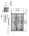
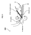
- a liquid-crystal display element therefor comprises a layered liquid-crystal panel which includes a pair of rectangular-shaped glass substrates each having a size of about 540 to 560 mm in length ⁇ about 950 to 970 mm in width ⁇ about 0.7 mm (700 ⁇ m) in thickness, and a liquid-crystal layer having a thickness of about 5 ⁇ m having a transparent electrode, a color filter etc. and sandwiched between the glass substrates, as shown in FIG. 2 .
- the liquid-crystal display element is typically has a polarizing sheet 11' commonly referred as "a polarizing plate" adhesively applied to each of a front side (viewing side) and a back side (backlight side) thereof.
- the polarizing sheet 11' is formed from a polarizing composite film 11 included in a flexible optical film 10 of a laminated structure, as shown in the perspective view at (Before Use) part of FIG. 1 , to have a rectangular shape with a size of 520 to 540 mm in length ⁇ 930 to 950 mm in width, as shown in the perspective view at (After Use) part of FIG. 1 .
- the liquid-crystal panel itself employed in the liquid-crystal display element is of an extremely thin structure having an overall thickness of about 1.4 mm (1400 ⁇ m).
- the optical film laminate 10 for use in forming the polarizing sheet to be laminated to the liquid-crystal panel W typically consists of a continuous web of flexible film which comprises the polarizing composite film 11, a surface-protection films 13 having an adhesive surface, and a carrier film 14.
- the polarizing film laminate 11 includes protective films laminated on the opposite surfaces of the polarizer, and an acrylic adhesive layer 12 formed on the side of the polarizer which is to be laminated to the liquid-crystal panel W.
- the carrier film 14 is releasably laminated to the adhesive layer 12 to provide a function of protecting the exposed side of the adhesive layer 12.
- the polarizing composite film 11 is prepared by subjecting a PVA (polyvinyl alcohol)-based film having a thickness of about 50 to 80 ⁇ m to a dyeing treatment using iodine and a cross-linking treatment; subjecting the obtained PVA-based film to an orientation treatment based on stretching in a lengthwise or widthwise direction thereof to form a continuous polarizer layer having a thickness of 20 to 30 ⁇ m, laminating a protective film to one or each of opposite surfaces of the formed continuous polarizer layer through an adhesive, and forming an acrylic adhesive layer 12 on one side of the polarizer to be laminated to the liquid-crystal panel W.
- a PVA polyvinyl alcohol
- a transparent TAC (triacetylcellulose)-based film having a thickness of about 40 to 80 ⁇ m is often used as the protective film for protecting the polarizer.
- the continuous polarizer layer will be simply referred as "polarizer”.
- polarizing composite film a film including a polarizer, a protective film laminated on one or both of opposite surfaces of the polarizer, and an adhesive layer formed on one side of the polarizer to be laminated to a liquid-crystal panel W, will be referred as "polarizing composite film”, and a sheet commonly called by the name “polarizing plate”, which is formed in a rectangular shape from the polarizing composite film, will be referred to as "polarizing sheet”.
- a polarizer typically has a thickness of about 20 to 30 ⁇ m, and, in case where two protective films are laminated on respective ones of opposite surfaces of the polarizer, the resulting laminate is increased in thickness by about 80 to 160 ⁇ m.
- an adhesive layer 12 formed on one side of the polarizer to be laminated to a liquid-crystal panel W has a thickness of about 10 to 30 ⁇ m, and thereby the thickness of the polarizing composite film 11 is increased to 110 to 220 ⁇ m in total.
- the polarizing composite films 11 are laminated to respective ones of the front and back sides of the liquid-crystal panel W in such a manner that polarizing axes interact each other at an angle of 90 degrees.
- the liquid-crystal display element in manufacturing a liquid-crystal display element for a widescreen television having a diagonal screen size of 42 inch, on an assumption that a thickness of a liquid-crystal panel itself is about 1400 ⁇ m, and the thickness of each of the polarizing composite films 11 is in the range of 110 to 220 ⁇ m, the liquid-crystal display element has an overall thickness of about 1620 to 1840 ⁇ m, which is still within 2.0 mm or less.
- the ratio of the thickness of the liquid-crystal element to the overall thickness of the liquid crystal panel W and the polarizing sheet 11' s about 10 : 1.5 to 10 : 3.
- the thickness of the polarizing composite film 11 itself can be reduced to 70 to 140 ⁇ m, so that an overall thickness of the resultant liquid-crystal display element is reduced to a range of about 1540 to 1680 ⁇ m, and the ratio of the thickness of the liquid-crystal element to that of the liquid crystal panel W and the polarizing sheet 11' will be in the range of about 10 : 1 to 10 : 2.
- An optical film 10 for use in a liquid-crystal display element has a structure as shown in the perspective view at (Before Use) part of FIG. 1 .
- the structure of the optical film 10 will be briefly described below, in connection with a manufacturing process thereof.
- An adhesive surface of a surface-protection film 13 having a thickness of about 60 to 70 ⁇ m is releasably laminated to the surface of a polarizing composite film 11 devoid of an adhesive layer, and a carrier film 14 is releasably laminated to the adhesive layer 12 provided on the surface of a polarizing composite film 11 which is to be laminated to a liquid-crystal panel W for providing a function of protecting the adhesive layer 12.
- the carrier film 14 generally serves as a carrying medium (carrier) for the polarizing composite film, as well as the means to protect the adhesive layer 12.
- a film having such functions will hereinafter be referred as a "carrier film”.
- the thickness of the adhesive layer 12 is in the range of 10 to 30 ⁇ m.
- a continuous web of the optical film 10 is continuously transferred and a plurality of slit lines are formed along transversely directed lines to a slit depth corresponding to a part of an overall thickness of the continuous web, such as a depth reaching the inner surface of the carrier film, then, the portion of the polarizing composite film 11 in the optical film 10 between two adjacent slit lines at the upstream and downstream sides as seen in the feed direction of the continuous web (for example, the lines defined by cutting only through the polarizing composite film 11 while keeping the carrier film 14 uncut), is peeled in the form of a polarizing sheet 11', and the peeled polarizing sheet 11' is laminated in a sequential manner to one surface of one of a plurality of liquid-crystal panels W being sequentially conveyed, the surface-protection film 13 and the carrier film 14 being those films which function to protect the respectively the non-adhesive surface and the adhesive surface of the polarizing
- one of the protective films for protecting the polarizer may be replaced with a phase difference film made of a cycloolefin-based polymer, a TAC-based polymer or the like and having an optical compensation function, and it may further be provided as a layer of a transparent substrate, such as a TAC-based substrate, having a polymer material, such as a polyester-based polymer or a polyimide-based polymer applied/arranged thereto and then cured.
- a polarizing composite film to be laminated to the backlight side of the liquid-crystal display element it may be possible to provide an additional function by laminating a brightness enhancement film to the backlight side protective film of the polarizer.
- the structure of the polarizing composite film 11 there have been proposed various other variations, such as a technique of laminating a TAC-based film to one of opposite surfaces of the polarizer and laminating a PET film to the other surface of the polarizer.
- One of methods for providing a polarizing composite film 11° including a polarizer and a protective film laminated on one or both of opposite surfaces of the polarizer with an adhesive layer 12 for attaching to a liquid-crystal panel W comprises laminating a carrier film 14 having a transferable adhesive layer formed thereon, to the surface of the polarizing composite film 11° to be laminated to the liquid-crystal panel W.
- a specific transfer technique is as follows.
- the carrier film 14 is subjected to a releasing treatment at the surface which is to be laminated to the polarizing composite film 11° at the surface of the polarizing composite film 11° which is to be laminated to the liquid-crystal panel W, and then a solvent containing adhesive is applied to the treated surface and dried to form an adhesive layer on the carrier film 14. Then, the carrier film 14 having the preliminarily formed adhesive layer 12 is laminated to the polarizing composite film 11°, for example, while continuously feeding the carrier film 14 unrolled from a carrier film roll and feeding the polarizing composite film 11° in the same manner, so that the adhesive layer formed on the carrier film 14 can be transferred to the polarizing composite film 11°. It is understood that the adhesive layer 12 may be formed by directly applying an adhesive containing solvent to the surface of the polarizing composite film 11° to be laminated to the liquid-crystal panel, and drying the same.
- the surface-protection film 13 typically has an adhesive surface layer. Unlike the adhesive layer on the polarizing composite film 11, the adhesive surface layer must be peeled off the polarizing sheet 11' together with a sheet (not shown) of the surface-protection film 13 when the sheet of the surface-protection film 13 is peeled off the polarizing sheet 11' during the manufacturing process of the liquid-crystal display elements. The reason is that the sheet of the surface-protection film 13 is provided for protecting the surface of the polarizing sheet 11', but not an adhesive surface to be transferred to the surface of the polarizing sheet 11'.
- the perspective view at (After Use) part of FIG. 1 shows the state after the sheet of the surface-protection film 13 is peeled and removed.
- the polarizing composite film 11 may be provided at the surface of the protective film on the front side of the polarizing composite film with a hard coat treatment for protecting the outermost surface of the liquid-crystal display element, and/or a surface treatment for obtaining an anti-glare effect or the like, such as an anti-glare treatment.
- liquid crystal display element By the way, for the function of the liquid crystal display element, the direction of orientation of liquid crystal molecules and the direction of polarization of the polarizer are closely related each other.
- LCDs Liquid-Crystal Display
- TN Transmission Nematic
- VA vertical Alignment
- IPS Inplane Switching
- liquid crystal molecules are provided between two upper and lower orientation films having respective rubbing directions on the inner surfaces of glass substrates of the liquid-crystal panel so that the liquid crystal molecules are twisted by 90 degrees along the optical axis, wherein, when a voltage is applied, the liquid crystal molecules are aligned in a direction perpendicular to the orientation films.
- the direction of rubbing on the orientation film at the viewing-side must be 45 degrees (the rubbing direction of the other orientation film is 135 degrees).
- the polarizing sheets made from the polarizing composite films for laminating respectively on the front and back sides of the liquid-crystal panel through adhesive layers 12 must have polarizers respectively oriented in directions inclined respectively by 45 degree with respect to a lengthwise or widthwise direction of the display screen so as to conform to the rubbing directions.
- an optical film for use in producing a liquid-crystal element of a TN-type liquid-crystal panel or in an optical film comprising a polarizing composite film which includes a polarizer subjected to an orientation treatment by stretching in a lengthwise or widthwise direction, a protective film laminated on the polarizer, and an adhesive layer formed on the side of the polarizer which is to be attached to the liquid-crystal panel, it is required that the optical film is punched or cut into a rectangular-shaped sheet having a major side or a minor side determined in accordance with the size of the TN liquid crystal panel and inclined by 45 degrees with respect to the orientation direction of the polarizer produced by the stretching in the lengthwise or widthwise direction, as described in Japanese Laid-Open Patent Publication JP 2003-161935A (Patent Document 1) or Japanese Patent 3616866 B (Patent Document 2).
- the punching or cutting the optical film into the rectangular-shaped sheet may be collectively referred as "individualized sheet” or "method and system for manufacturing individualized sheet” for a liquid-crystal display element.
- the sheet of the optical film thus punched or cut is produced by punching or cutting in the form including the protective carrier film so that any exposure of the adhesive layer in the polarizing composite film contained in the optical film can be prevented.
- the punched-out or cut sheet of the carrier film may be referred as "separator", rather than "sheet of the carrier film”.
- the manufacturing process of the liquid-crystal display elements includes the first step of peeling the separator from each of the sheet of the optical film to have the adhesive layer exposed.
- the sheets of the optical film each having the adhesive layer exposed by peeling the separator are conveyed one-by-one by for example under a vacuum suction irrespective of whether the surface protective films are laminated or not, and laminated to respective ones of a plurality of liquid-crystal panels.
- the punched-out or cut sheet is in the form of an individualized sheet having four trimmed sides and a certain level of stiffness.
- this polarizing sheet having four trimmed sides has generally been called as "polarizing plate" which is still used as a common name.
- an optical film unwound from a roll of the optical film may be sequentially punched or cut in a direction transverse to the feed direction, with the result that the polarizing sheets contained in the formed sheets are also simultaneously formed in a desired shape.
- the polarizing sheets each formed with a major or minor side extending in a direction 45 degrees with respect to the orientation direction of a polarizer produced by stretching in a lengthwise or widthwise direction i.e., with respect to the feed direction of the optical film prior to the punching or cutting process
- a polarizing composite film having a width greater than a major side of a liquid-crystal panel, or an optical film comprising such polarizing composite film is transported in a lengthwise direction, and punched at an angled direction of 45 degrees with respect to the lengthwise direction, using a die into a plurality of individual polarizing sheet as seen in the Patent Document 1 or 2.
- an elongated polarizing composite film may be provided in the form of a single sheet from an optical film having a substantially large width by punching or cutting it in a direction 45 degrees inclined with respect to the lengthwise direction, or connecting a plurality of such sheets into a film-like configuration, and winding the film to form a roll of the polarizing composite film or the optical film including the polarizing composite film, the elongated polarizing composite film being then used in a process of forming polarizing sheets, by unwinding the polarizing composite film or the optical film including the polarizing composite film from the roll, and cutting into a required size to form a plurality of polarizing sheets or sheets of the optical film, each of the polarizing sheets or the sheets of the optical film being then laminated to a respective one of a plurality of liquid-crystal panels W being sequentially fed, to complete a liquid-crystal display element.
- the above techniques are not beyond the system for manufacturing individualized sheets.
- Patent Document 3 discloses a technique of continuously feeding an optical film which comprises a polarizing composite film (in the Patent Document 3, termed as "elongated polarizing plate") and a separator for protecting an adhesive layer on the polarizing composite film onto a plurality of liquid-crystal panels (in the Patent Document 3, termed as "liquid-crystal cells") for constituting small-size display screens of electronic calculators or the like utilizing a carrier function of the separator, "cutting only the polarizing plate 4 and the adhesive layer 5 while leaving the separator 6 uncut (hereinafter referred as "half-cut”)", removing defective sheets of polarizing sheets formed by the half-cut process in the course of the feeding, and sequentially laminating the remaining polarizing sheets to respective ones of the plurality of liquid-c
- the apparatus may be a so-called "labeler unit".
- this liquid-crystal panel is an LCD using a TN-type liquid crystal, so that the optical film herein used must be an elongated sheet produced form an optical film having a substantially large width by cutting it in a direction 45 degrees oblique to the longitudinal direction of the optical film with a width corresponding to the width of the liquid-crystal panel, or a film-like strip formed by connecting a plurality of such optical film sheets.
- This technique is based on the use of an elongated polarizing sheet which is cut in a direction 45 degrees oblique to the stretched direction of the polarizing composite film with a width corresponding to the width of the liquid-crystal panel, so that it cannot be practically applied directly to an optical film continuous feed apparatus for use in continuous manufacturing of a large-size liquid-crystal display element for widescreen televisions.
- a plurality of inspected individualized sheets formed from an optical film in an optical film manufacturing line and preliminarily subjected to inspection for the presence or absence of any defect are carried into a liquid-crystal display element manufacturing line in a batch.
- the carried-in individualized sheets are manually stored in a polarizing-sheet magazine.
- the adhesive layer in each of the stored individualized sheets has a separator laminated thereto to protect the adhesive layer from exposure.
- the magazine storing the polarizing sheets is incorporated in the liquid-crystal display element manufacturing line.
- liquid-crystal panel magazine which is incorporated in the same manufacturing line and stores a plurality of liquid-crystal panels, and a plurality of liquid-crystal panels are taken out one-by-one from the liquid-crystal panel magazine and conveyed through a cleaning/polishing step.
- the individualized sheets are taken out one-by-one from the polarizing-sheet magazine by means of a suction-type conveyor unit.
- the individualized sheets thus taken out are typically passed through a step of peeling the separator to expose the adhesive layer in the polarizing composite film, and conveyed to a position for lamination with the liquid crystal panels, and laminated to respective ones of the liquid crystal panels in a registered relation with the liquid crystal panel, to continuously produce the liquid-crystal display elements.
- This method is disclosed, for example, in Japanese Laid-Open Patent Publication No. 2002-23151A (Patent Document 4).
- the manufacturing process utilizing such individualized sheets has problems not only in that the separators must be removed from respective ones of the individualized sheets taken out from the magazine, but also in that the individualized sheets are flexible and likely tend to be curved or distorted while they are being carried under suction, so that difficulties have been encountered in maintaining accuracy and speed in automatic registration and automatic lamination with liquid-crystal panels.
- the individualized sheet is required to have a certain level of thickness and stiffness to facilitate transport under suction and handling for automatic laminating process.
- Patent Document 5 Japanese Laid-Open Patent Publication No. 2004-144913A
- Patent Document 6 Japanese Laid-Open Patent Publication No. 2005-298208A
- Patent Document 7 Japanese Laid-Open Patent Publication No. 2006-58411A
- the VA-type and IPS-type liquid-crystal panels are not designed to arrange liquid crystal molecules in twisted orientations.
- these types of liquid-crystal panels there is no need to have the polarization axis of the polarizing sheet oriented 45 degrees with respect to the direction of the long or short side of the liquid-crystal display element, as having been required in the TN-type liquid-crystal panel because of the field-of-view characteristics inherent to the orientation of the liquid crystal molecules, but only required to have the polarizing sheets applied to the opposite sides of the liquid crystal display panel oriented with their polarization axes crossed at 90 degrees crossing angle.
- the polarizing sheets of these types has a feature that an optical film including a polarizing composite film which has been subjected to a longitudinal or transverse stretching can be continuously unwound from a roll and cut along transverse lines to sequentially produce rectangular polarizing sheets.
- Patent Document 8 which is based on use of the VA-type or IPS-type liquid-crystal panels and comprises steps of continuously feeding an optical film laminate, cutting an optical film laminate in conformity to the size of a liquid-crystal panel and sequentially laminating polarizing sheets which have been produced by the cutting step and contained in the optical film, to respective ones of a plurality of the liquid-crystal panels.
- the subjects and the concepts of the present invention are close to and inseparably linked with manufacture of a liquid-crystal display element using a liquid crystal such as the VA-type and IPS-type liquid crystals which are different in principle from the TN-type liquid crystal, , as described later.
- a liquid crystal such as the VA-type and IPS-type liquid crystals which are different in principle from the TN-type liquid crystal, , as described later.
- normal regions are defined as regions having no defect as shown in FIG. 3 and defect-free polarizing sheets (hereinafter referred as "normal polarizing sheets”) are punched out or cut from the polarizing composite film, appropriately avoiding defective regions having a defects therein.
- the defective regions are also punched out or cut from the polarizing composite film, as defective sheets (hereinafter referred as "defective polarizing sheets”), and only the defective polarizing sheets are selectively removed.
- the process is required to comprise the steps of first feeding a continuous web of optical film including a polarizing composite film; locating a defect or defects in the polarizing composite film which is being fed as a component of the continuous web, to preliminarily define regions of the optical film into defective regions and normal regions, based on positions or coordinates of the defects, and in addition, in case for example where the optical film includes a carrier film releasably laminated to the polarizing composite film, during the course of feeding the continuous web of the optical film, forming a plurality of cut lines in the continuous web transversely to the feed direction of the continuous web to a depth reaching the inner surface of the carrier film, whereby only portions of the polarizing composite film between each adjacent two or each pair of upstream and downstream side ones of the cut lines as seen in the feed direction of the continuous web are cut to thereby
- the surface-protection film with a function of carrier whereby the carrier film which will otherwise be retained without being cut when the cut lines are formed in the optical film, may be cut together with the polarizing composite film.
- the carrier film is cut into a plurality of sheets (so-called "separators"), so that it is necessary to provide an additional step of peeling the separators from the normal polarizing sheets when the normal polarizing sheets are laminated to the corresponding ones of the liquid-crystal panels.
- the surface-protection film having such carrier function may be used in place of the carrier film.
- Patent Document 9 Japanese Laid-Open Patent Publications 2005-62165A (Patent Document 10) and 2007-64989A (Patent Document 11).
- Patent Document 9 Japanese Laid-Open Patent Publications 2005-62165A
- Patent Document 11 Japanese Laid-Open Patent Publications 2005-62165A
- Patent Document 11 2007-64989A
- the first step comprises inspecting defects contained in the polarizing composite film or the polarizer being continuously fed to determine positions or coordinates of the defects through image processing, encoding the information obtained by the image processing, and then directly printing the encoded information on marginal or edge portion of the polarizing composite film or polarizer which will be left in the web after a subsequent step of punching or cutting the polarizing composite film or polarizer during the production of the individualized sheets, and winding the resulting polarizing composite film or polarizer to form a roll.
- the second step comprises incorporating the roll into a manufacturing line, using a reading device to read the encoded information printed on the polarizing composite film or polarizer unrolled from the roll, and providing marks at the positions of the defects based on the results of determination on the presence of defects, followed by subsequent steps of: punching or cutting for producing individualized sheets from the polarizing composite film or polarizer, and sorting the individualized sheets produced by punching or cutting into normal defective polarizing sheets.
- the above steps have been technical means essential to improving yield in the manufacture of such individualized sheets.
- the polarizing composite film or polarizer is termed as "sheet-shaped member", and "for example, a polarizing composite film, a phase difference film, an plastic sheet for organic electroluminescent (EL) elements, a plastic sheet for liquid-crystal cells, and a plastic sheet for solar battery boards" are described.
- the sheet-shaped member includes a polarizing sheet which has a polarizer and two protective films laminated to respective ones of opposite surfaces of the polarizer, and a sheet to be punched out or cut is termed as "product”.
- a polarizing composite film or a polarizer is termed as "polarizing plate stock", and a punched-out or cut sheet is termed as "sheet-shaped product".
- Patent Documents 9 to 11 disclose as the first manufacturing process a process comprising the steps of: using a preliminary inspection device to detect positions or coordinates of defects present in the "sheet-shaped member” or the “polarizing plate stock", encoding the detected information, using a recording device to print the encoded information onto the "sheet-shaped member” or “polarizing plate stock” in such a manner as to be readable by a reading device when a "product” or a "sheet-shaped product” is punched out or cut from the "sheet-shaped member” or “polarizing plate stock”; and forming a wound roll of the resulting the "sheet-shaped member” or “polarizing plate stock".
- the Patent Documents 9 to 11 also disclose a second manufacturing process of the "sheet-shaped member” or “polarizing plate stock” using a wound roll.
- the second manufacturing process comprises the steps of: making a mark directly to a position or coordinate of a defect of the "sheet-shaped member” or “polarizing plate stock”, based on encoded information preliminarily printed on the "sheet-shaped member” or “polarizing plate stock” and read by the reading device; punching or cutting the "sheet-shaped member” or “polarizing plate stock” being fed out from the wound roll; and allowing a "product” or “sheet-shaped product” punched out or cut from the "sheet-shaped member” or “polarizing plate stock” to be sorted into a normal product and a defective product.
- Patent Document 12 a manufacturing method wherein an optical film (in the Patent Document 12, termed as "polarizing plate stock”) is continuously unrolled from a roll of the optical film which is the form of a laminated structure, a carrier film (in the Patent Document 12, termed as “releasable film”) is peeled from the laminate of the optical film before the polarizing composite film in the optical film is inspected for existence of defects, then after the inspection, the polarizing composite film is punched or cut avoiding positions of defects while leaving the defects on the web to provide rectangular sheets only by non-defective regions of the polarizing composite film to produce normal polarizing sheets (in the Patent Document 12, termed as "sheet-shaped products”) which are transported by means of another carrier medium to a laminating position.
- polarizing plate stock an optical film
- releasable film in the Patent Document 12
- this process is not the one which makes it possible to transport only the produced normal polarizing sheets to the position for lamination with a liquid-crystal panel by means of the continuous web of the optical film. It should be referred that this technique is not beyond the individualized sheet manufacturing system.
- This invention is a method and apparatus for manufacturing liquid-crystal display elements comprising the following steps.
- the method comprises a step of peeling a first carrier film which is provided for protecting an adhesive layer of a polarizing composite film contained in the optical film.
- the method further comprises steps of: preliminarily inspecting a defect in the polarizing composite film having the adhesive layer exposed by peeling the first carrier film, and then feeding a second carrier film and releasably laminating the second carrier film to the exposed adhesive layer of the polarizing composite film to provide again a protection for the adhesive layer so as to maintain a continuous web of optical film comprising the polarizing composite film.
- the method further comprises steps of forming a plurality of cut lines in the continuous web of optical film along a direction transverse to the feed direction of the continuous web, the positions of the cut lines being determined in accordance with the defective regions containing defects in the polarizing composite film and non-defective, normal regions having no defects as determined by the results of the inspection for the existence of defects in the polarizing composite film, the cut lines being formed to a depth reaching the inner surface of the second carrier film to thereby define defective polarizing sheets and normal non-defective polarizing sheets, between respective longitudinally adjacent two of the cut lines located upstream side and downstream side in the feed direction, only the defective polarizing sheets being automatically removed from the second carrier film before the defective and normal polarizing sheets reach to the position for laminating on respective ones of a plurality of liquid-crystal panels being sequentially conveyed, whereby only the normal polarizing sheets left on the second carrier film are transported to laminating position for lamination with the liquid-crystal panels.
- the method comprises the step of peeling the normal polarizing sheets from the second carrier film, and laminating each of the peeled normal polarizing sheets on one of opposite surfaces of each of the liquid-crystal panels.
- This invention contains an innovative proposal allowing for shifting from the individualized sheet manufacturing system designed to preliminarily form a plurality of individualized sheets, and laminate the individualized sheets to respective ones of a plurality of liquid-crystal panels, to a serial-type polarizing sheet manufacturing system designed to continuously form a plurality of serial-type polarizing sheets, and laminate the serial-type polarizing sheets to respective ones of a plurality of liquid-crystal panels.
- the technical challenge of the aforementioned invention has been how to realize the technical measures for forming a plurality of cut lines in the continuous web of optical film transverse to the feed direction of the continuous web at two spaced apart positions between upstream and downstream sides in the feed direction to a depth reaching the inner surface of the second carrier film, to form defective polarizing sheets and normal polarizing sheets corresponding respectively to the preliminarily defined defective and normal regions in the polarizing composite film, on the second carrier film which has been left uncut, and automatically removing only the defective polarizing sheets from the second carrier film.
- the technical challenge was solved by providing steps of, for the preparation of a preliminary inspection for defining the defective normal regions, separating the continuous web of the optical film from the carrier film and/or the surface-protection film adopted as temporary process materials to be used in the production of liquid-crystal display elements, and after the preliminary inspection, laminating a substitute carrier film and/or a substitute surface-protection film again on the continuous web of optical film.
- steps are essential to protect the adhesive layer and the obverse surface of the polarizing composite film from exposure thereof during the manufacturing process of liquid-crystal display elements.
- US-A-2005/0016670 describes a method and apparatus for bonding a polarizing plate high in operating efficiency and yield.
- the apparatus includes a cutting unit for cutting at least a polarizing plate of a strip-shaped film, composed of the polarizing plate and a release film bonded to the polarizing plate, leaving the release film uncut, when a forward end side pre-severed end face of the strip-shaped film perpendicular to the longitudinal direction of the strip-shaped film has travelled up to a length corresponding to a length of a substrate, to form a film piece, a release film separating unit for separating the release film from the film piece thus severed, and a bonding unit for bonding the tacky surface of the film piece freed of the release film to a mating position of the substrate so that the forward end side end face of the transported substrate is parallel to the pre-severed end face of the film piece.
- the present invention has been made based on the above related inventions and through intensive researches and considerations for significantly enhancing product accuracy and manufacturing speed, and drastically improving production yield, in the manufacture of liquid-crystal display elements.
- the present invention provides a roll of an optical film laminate for use in a continuous manufacturing method and system for liquid-crystal display elements wherein the continuous manufacturing method and system are configured for unrolling a continuous web of optical film from the roll under a tension, forming a plurality of slit lines in the unrolled continuous web of optical film along a direction transverse to the feed direction of the continuous web at a plurality of pairs of upstream and downstream positions in the feed direction to a depth reaching the inner surface of the carrier film in the optical film laminate, to form, on the carrier film being left uncut under the cut lines, defective polarizing sheets corresponding to defective regions in the polarizing composite film and defect-free, normal polarizing sheets corresponding to defect-free or normal regions each having a size suitable for being laminated to each of a plurality of liquid-crystal panels, feeding these sheets by means of the carrier film by holding them in a releasable manner on the carrier film and during that time, automatically removing the defective polarizing sheets to allow only the normal polarizing sheets
- This makes it possible to significantly enhance the product accuracy and manufacturing speed and drastically improve the production yield, in the manufacture of liquid-crystal display elements.
- the surface-protection film may be configured to possess a carrier function so that the polarizing sheets produced by cutting at the slit lines are conveyed by the surface-protection film.
- the carrier film laminated on the adhesive layer of the polarizing composite film in a releasable manner is also cut along the slit lines together with the polarizing composite film having the adhesive layer to form a plurality of polarizing sheets, so that, it is necessary to provide additional technical measures for separating sheets of the carrier film which may be referred as separators, from respective ones of the polarizing sheets when each of the polarizing sheets is laminated on the corresponding one of the liquid-crystal panels.
- the invention provides a method of producing a roll of optical film laminate as in claim 1.
- the invention may be further characterized in that the encoded information further includes information for identifying the defective region and the normal region of the polarizing composite film.
- the invention may be further characterized in that the step of forming the web of the optical film includes a further step of releasably laminating a surface-protection film having an adhesive surface on the polarizing composite film at a surface opposite to the surface on which the carrier film is releasably laminated.
- the invention may be further characterized in that the encoded information is recorded on the carrier film or the surface-protection film.
- the invention may be further characterized in that the carrier film has a transferable adhesive layer formed by, after subjecting one surface of the carrier film to a releasing treatment, applying a solvent containing an adhesive to the treated surface, and drying the solvent.
- the invention may be further characterized in that the step of detecting the location or the coordinate position of the defect includes a first inspection sub-step of primarily inspecting the surface of the polarizing composite film by means of reflected light, and a second inspection sub-step of primarily inspecting the inside of the polarizing composite film by means of transmission or cross-Nicol transmission.
- the invention may be further characterized by the polarizing composite film having a width conforming to a long or short side of each of the liquid-crystal panels.
- the invention may be further characterized in that the encoded information further includes information for identifying the defective region and the normal region of the polarizing composite film.
- the invention may be further characterized in that the step of forming the web of the optical film comprises a further step of releasably laminating a surface-protective film having an adhesive surface on the polarizing composite film at the surface opposite to the surface on which the carrier film is releasably laminated through the adhesive layer.
- the invention may be further characterized in that the encoded information is recorded on the carrier film or the surface-protection film.
- the invention may be further characterized in that the provisional carrier film has a transferable adhesive layer formed by, after subjecting one surface of the provisional carrier film to a releasing treatment, applying a solvent containing an adhesive to the treated surface, and drying the solvent.
- the invention may be further characterized in that the carrier film is subjected to only a releasing treatment at a surface through which the carrier film is releasably laminated on the polarizing composite film which has been fed with the adhesive layer in an exposed state.
- the invention may be further characterized in that the step of detecting the location or the coordinate position of the defect includes a first inspection sub-step of primarily inspecting a portion of the surface of the polarizing composite film devoid of the adhesive layer by means of reflected light, and a second inspection sub-step of primarily inspecting the inside of the polarizing composite film by means of transmission or cross-Nicol transmission.
- the invention may be further characterized by the polarizing composite film having a width conforming to a long or short side of each of the liquid-crystal panels.
- the invention provides a system as in claim 12.
- the invention may be characterized in that the encoded information further includes information for identifying the defective region and the normal region of the polarizing composite film.
- optical-film forming unit further includes a lamination mechanism for laminating the polarizing composite film to a surface-protective film, the lamination mechanism being adapted to releasably laminate a surface-protection film having an adhesive surface on the polarizing composite film at a surface opposite to the surface on which the carrier film is releasably laminated.
- the invention may be characterized in that the encoded information is recorded on the carrier film or the surface-protection film.
- polarizing composite film inspection unit includes a first inspection sub-unit adapted to primarily inspect the surface of the polarizing composite film by means of reflected light, and a second inspection sub-unit adapted to primarily inspect the inside of the polarizing composite film by means of transmission or cross-Nicol transmission.
- the invention may be characterized by the polarizing composite film having a width conforming to a long or short side of each of the liquid-crystal panels.
- the invention may be characterized in that the encoded information further includes information for identifying the defective region and the normal region of the polarizing composite film.
- the invention may be characterized in that the optical-film forming unit further including a lamination mechanism for laminating a surface-protective film on said polarizing composite film having said adhesive layer, the lamination mechanism being adapted to releasably laminate the surface-protection film having an adhesive surface on the polarizing composite film at a surface opposite to the surface on which said carrier film is releasably laminated.
- the invention may be characterized in that the encoded information is recorded on the carrier film or the surface-protection film.
- polarizing composite film inspection unit includes a first inspection sub-unit adapted to primarily inspect the surface of the polarizing composite film having the adhesive layer by means of reflected light, and a second inspection sub-unit adapted to primarily inspect the inside of the polarizing composite film having the adhesive layer by means of transmission or cross-Nicol transmission.
- the invention may be further characterized by the polarizing composite film having a width conforming to a long or short side of each of the liquid-crystal panels.
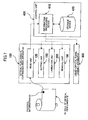
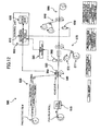
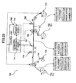
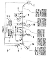
- FIG. 5 is a schematic diagram showing a continuous manufacturing system for liquid-crystal display element 1 which comprises an optical-film feed apparatus 100 having a roll of an optical film laminate for manufacturing liquid-crystal display elements according to the present invention, and a liquid-crystal-panel conveyance apparatus 300 for conveying liquid-crystal panels to be laminated with normal polarizing sheets formed from a continuous web of the optical film fed from the roll.
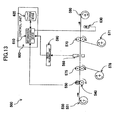
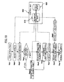
- FIG. 6 is a flowchart showing a manufacturing process or process steps in the continuously manufacturing system for liquid-crystal display element 1 illustrated in FIG. 5 .
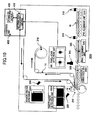
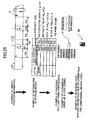
- the optical-film feed apparatus 100 comprises a support rack 110 for rotatably mounting a roll of optical film laminate 10 according to one embodiment of the present invention, a reading unit 120 for reading encoded information, a film feed unit 130 including a feed roller, a speed adjustment unit 140 including a dancer roller for providing a constant speed film feeding, a slitting unit 150 for forming slits in the continuous web of the optical film in a direction transverse to the feed direction of the continuous web with a depth reaching the inner surface of the carrier film to form slit lines, a slit-position check unit 160 for checking the formed slit lines, a film feed unit 170 including a feed roller, a speed adjustment unit 180 including a dancer roller for providing a constant speed feeding, a defective-polarizing-sheet removal unit 190 for peeling and removing a slit defective polarizing sheet from the carrier film, a lamination unit 200 including a pair of lamination rollers for applying a normal polarizing sheet which has been slit and peele
- the roll of optical film laminate 10 according to this embodiment installed in the optical-film feed apparatus 100 has a width approximately equal to a length of a long or short side of a liquid-crystal panel to which it is applied. It is preferable that a transparent protective film is used for the protective film laminated on one or each of the opposite surfaces of the polarizer as shown in the schematic diagram of FIG. 1 .
- the roll of optical film laminate 10 comprises a roll of an optical film laminate comprising a continuous web of an optical film comprised of a polarizing film laminate 11 including a polarizer having an adhesive layer 12 provided on the surface of the polarizer which has a transparent protective film laminated thereon and which is to be attached to a liquid-crystal panel, a surface-protection film 13 having an adhesive surface which is releasably laminated on the surface of the polarizing composite film 11 opposite to the surface having the adhesive layer 12, and a carrier film 14 releasably laminated on the adhesive layer 12 of the polarizing composite film 11.
- the carrier film 14 is a releasable film adapted to protect the adhesive layer 12 of the polarizing composite film 11 during the manufacturing process of liquid-crystal display elements and to be removed by being taken up when the polarizing sheet formed in the continuous web of optical film is peeled off prior to or during lamination process for attaching the polarizing sheet to the liquid-crystal panel.
- the term "carrier film” is used since the film has a function of carrying the normal polarizing sheets in the optical film 10 to the laminating position.
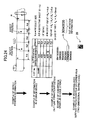
- the roll of optical film laminate 10 is formed as follows. Details of the manufacturing method for the roll of optical film laminate 10 will be described later. During the manufacturing process of the roll of optical film laminate 10, defects existing in the polarizing composite film 11 are first detected in the continuous web of the optical film being continuously fed using an inspection unit. Then, based on the detected locations or coordinate positions of the defects in the polarizing composite film 11, defective regions and defect-free, normal regions are defined in the polarizing composite film 11 as shown in FIG. 3 . Then, information including slit-position information, and optionally identification information for identifying the defective regions and the normal regions is recorded on the continuous web of the optical film being continuously fed.
- the slit-position information is providing for indicating the positions at which respective ones of the slit lines are to be formed in the continuous web of the optical film, and the slit lines are formed in pairs by the slitting unit 150 of the continuous manufacturing system 1 based on the defective and normal regions of the polarizing composite film 11, during the manufacturing process of liquid-crystal display elements, in a manner as to slit the continuous web of optical film being fed in a direction transverse to the feed direction of the web to a depth reaching the inner surface of the carrier film so that slit lines are formed at upstream and downstream positions as seen in the feed direction.
- the information including the slit-position information and the optional identification information to be recorded on the continuous web of optical film is encoded information created together with or in association with additional information, such as information relating to the manufacturing lot and the length of the web in the roll.
- the encoded information is recorded on the carrier film 14 in the continuous web of the optical film to be continuously fed.
- the encoded information may be recorded on the carrier film 14 in any of variety of modes, such as a mode in which encoded information including all necessary information is recorded on a single location, or a mode in which a plurality of encoded information each including different information is recorded on a plurality of storage locations at given intervals (e.g., at intervals of 1 m or 100 m).
- the encoded information may be recorded on the surface-protection film 13, instead of the carrier film 14. In either case, the encoded information is configured to be readable by the reading unit 120 of the continuous manufacturing system 1.
- the slitting unit 150 provided in the continuous manufacturing system for liquid-crystal display element 1 having the roll of optical film laminate 10 mounted thereon is operated, during the manufacturing process of the liquid crystal display element, by having the measurement data on an optical-film feed-out distance calculated when the continuous web of optical film is unrolled from the roll of optical film 10 related with the slit-position information included in the encoded information and read by the reading unit 120 of the continuous manufacturing system 1.
- the region of the polarizing composite film defined by adjacent two slit lines may include a defect-free, normal region having a give length determined by the length of a side of a liquid-crystal panel to be laminated with the polarizing composite film, and a defective region having a length generally less than the given length.
- the defective region of the polarizing composite film 11 which is cut along pairs of slit lines by means of the slitting unit 150 is defined as a defective polarizing sheet X ⁇ which is to be removed from the continuous web of optical film (specifically, the carrier film 14) by the defective polarizing sheet removal unit 190 of the continuous manufacturing system 1.
- the normal region of the polarizing composite film 11 is cut in the same manner and defined as a normal polarizing sheet X ⁇ which is peeled off from the continuous web of optical film (specifically, the carrier film 14) and laminated to one of opposite surfaces of a liquid-crystal panel by means of the lamination unit 200 of the continuous manufacturing system 1.
- the normal region is preliminarily defined in accordance with the locations or the coordinate positions of defects in the polarizing composite film 11 as described later, and the length (X ⁇ ) of the normal region is determined to a constant value in accordance with the length of one of the sides of the liquid-crystal panel which is to be laminated with the normal polarizing sheet.
- the upstream side slit line for defining the defective region is defined by the downstream side slit line defining the normal region which is located immediately upstream side of the defective region, as seen in the feed direction of the web.
- the length (X ⁇ ) of the defective region is determined by the upstream side slit line and a downstream side slit line which is formed slightly downstream side of the location or coordinate position of a defect. Since the length between the upstream slit line of the defective region and the location or coordinate position of defects may not be fixed, the length (X ⁇ ) of the defective region varies accordingly.
- the length (X ⁇ ) of the defective region is determined through an information processing, when a processing is made for determining the slit position information which designates the position at which the slit line is to be formed, so that it is always different from the length (X ⁇ ) of the normal region, e.g., to establish the relationship X ⁇ ⁇ X ⁇ , in any case.
- information X ⁇ is produced to identify the defective region over the normal region, when the length (X ⁇ ) of the defective region becomes equal to the length (X ⁇ ) of the normal region.
- the produced identification information X ⁇ is incorporated into the encoded information together with and in association with the slit-position information.
- the continuous manufacturing system 1 is configured such that, during the manufacturing process of liquid-crystal display elements, the slitting unit 150 of the continuous manufacturing system for liquid-crystal display elements 1 functions to form the normal polarizing sheet X ⁇ and the defective polarizing sheet X ⁇ according to the slit-position information read by the reading unit 120 of the continuous manufacturing system 1, and the defective-polarizing-sheet removal unit 190 of the continuous manufacturing system 1 functions to readily discriminate and remove only defective polarizing sheets having lengths (X ⁇ ) different from the length (X ⁇ ) of the normal region.
- the encoded information includes the identification information X ⁇ for identifying the defective region over the normal region
- the defective polarizing sheet removal unit 190 of the continuous manufacturing system 1 functions, based on the identification information, to discriminate and remove only defective polarizing sheets.
- the roll of optical film laminate 10 is mounted on the support rack 110 of the optical-film feed apparatus 100.
- the support rack 110 is provided with an encoder (not shown) for determining the feed-out distance of the continuous web of the optical film
- the measurement data obtained by the encoder is stored in a storage device 420 of a control unit 400.
- a measurement device may additionally be provided in the optical-film feed apparatus 100 for calculating the feed-out distance of the continuous web of the optical film.
- a roll of dummy film is first installed on the continuous manufacturing system for liquid-crystal display element 1.
- a continuous web of dummy film is fed from the roll of dummy film under tension by means of first and second film feed units 130, 170 each including feed rollers.
- the continuous web of dummy film is advanced until its leading edge reaches a position where, under a normal operation, the normal polarizing sheet X ⁇ is peeled off from the carrier film 14, the carrier film 14 from which the normal polarizing sheet is peeled off is passed through the lamination unit 200 and taken up by the carrier-film take-up drive mechanism 210.
- first and second speed adjustment units 140, 180 each including the aforementioned dancer rollers immediately before these positions.
- a single such continuous manufacturing system 1 will be operated by being sequentially connected with 5 to 20 rolls of the optical film laminate in a day.
- the continuous manufacturing system 1 using the roll of the optical film according to this embodiment makes it possible to enhance product accuracy and double the manufacturing speed. If a plurality of liquid-crystal panels W can be sequentially fed without any problem, the number of the rolls of the optical film laminate to be handled will increase significantly, which gives rise to a new technical need for automatic replacement of the roll of the optical film laminate.
- the normal polarizing sheet of the polarizing composite film 11 cut along two adjacent slit lines in the continuous web of the optical film is peeled off from the carrier film 14 immediately before the lamination unit 200, and the normal polarizing sheet having the exposed adhesive layer 12 is laminated to a liquid-crystal panel through the adhesive layer 12.
- the carrier film 14 is taken up by the carrier-film take up drive mechanism 210.
- the surface-protection film 13 is made to be a sheet configuration which is held together with the normal polarizing sheet of the polarizing composite film 11 which is to be laminated to a liquid-crystal panel, and the sheet of the surface-protection film is peeled and removed after the final step including cleaning/drying is carried out on the liquid-crystal display element to be produced.
- Both of the carrier film and the surface-protection film are manufacturing-process materials required for carrying out the process, but are removed in the final stage of the manufacturing process and discarded.
- description will solely be made with regard to an example wherein only the carrier film is utilized as a manufacturing-process material used for the information storing medium.
- FIG. 7 is a schematic diagram showing a relation between the encoded information 20 to be read by the reading unit 120 of the continuous manufacturing system 1 and processed by an information processing device 410, and the previously described control unit 400 for controlling each of the units respectively provided in the optical-film feed apparatus 100 (see FIG. 5 ) and the liquid-crystal-panel conveyance apparatus 300 (see FIG. 5 ) for sequentially conveying the liquid-crystal panels.
- the encoded information 20 recorded in the roll of optical film laminate 10 includes the slit position information indicative of positions where the respective slit lines are to be formed in the continuous web of the optical film, and optionally the identification information for identifying the defective region over the normal region.
- the continuous web of the optical film 10 is continuously fed, and defects existing in the polarizing composite film 11 included in the continuous web of the optical film 10 are detected by the inspection unit to determine defective and normal regions in the polarizing composite film 11 based on the locations or the coordinate positions of the detected defects, whereby the slit lines are formed in pairs by the slitting unit 120 of the continuous manufacturing system 1, base on the defective and normal regions of the polarizing composite film 11, during the manufacturing process of liquid-crystal display elements, so that the continuous web of the optical film is slit in a direction transverse to the feed direction thereof at the two adjacent positions or the upstream and downstream positions in the feed direction to a depth reaching the inner surface of the carrier film.
- the encoded information 20 is recorded on the continuous web of optical film, preferably on the carrier film.
- the recorded encoded information 20 is read by the reading unit 120 including a code reader or a CCD camera, and the encoded information 20 read in this manner is transmitted to the information processing device 410 included in the control unit 400 of the continuous manufacturing system 1.
- the encoded information 20 read by the reading unit 120 is transmitted to the information processing device 410, and then the information processing device 410 functions to appropriately process the received encoded information 20.
- the control unit 400 is also operable, based on the encoded information 20 processed by the information processing device 410, to systematically control respective units included in the liquid-crystal-panel conveyance apparatus 300, and the optical-film feed apparatus 100, such as the slitting unit 150, the defective-polarizing-sheet removal unit 190 and the lamination unit 200, in an inter-related manner.
- the control unit 400 Based on the slit-position information included in the processed encoded information, the control unit 400 functions to control the operation of the film feed unit 130 including the feed rollers to feed the continuous web of the optical film and then control the operation of the first speed adjustment unit 140 to temporarily stop the feed of the continuous web of the optical film. Then, the control unit 400 functions to control the operation of the slitting unit 150 to form slits in the continuous web of the optical film in a direction transverse to the feed direction of the continuous web of the optical film at the two adjacent positions or the upstream and downstream positions in the feed direction to a depth reaching the inner surface of the carrier film 14, to form a plurality of slit lines in the continuous web of the optical film.
- the continuous web of the optical film having the slit lines formed thereon is transported to the slit-position checkup unit 160 where the slit line positions on the web are confirmed. Then, the defective polarizing sheets and the normal polarizing sheets formed by the slit lines in the continuous web of the optical film are identified or discriminated from each other, for example, based on the difference in length, at the defective-polarizing-sheet removal unit 190 inter-related with the film feed unit 170 including feed rollers and the speed adjusting unit 180, and only the defective polarizing sheets are peeled and removed from the carrier film 14.
- encoded information includes the identification information for identifying the defective polarizing sheet over the normal polarizing sheet
- the defective-polarizing-sheet removal unit 190 to peel and remove only the defective polarizing sheets from the carrier film 14 based on the identification information.
- the continuous web of the optical film from which the defective polarizing sheets are removed is then transported by the carrier-film take-up drive mechanism 210, in synchronization with the feed of the liquid-crystal panels being sequentially conveyed.
- the carrier film 14 is taken up at a position where the leading edge of the normal polarizing sheet defined by the slit lines in the polarizing composite film reaches the leading edge of the conveyed liquid-crystal panel, where the normal polarizing sheet is peeled off and the lamination unit 200 including the pair of lamination rollers starts laminating operation to attach the normal polarizing sheet to a corresponding one of the liquid-crystal panels.
- liquid crystal display elements will now be described with respect to specific operations of the respective units operated by the control unit 400, including the laminating operation of the lamination unit 200 to attach the normal polarizing sheet to a corresponding one of the liquid-crystal panels.
- the defective sheet removal unit 190 is operated under the control of the control unit 400 to identify or discriminate only the defective polarizing sheet X ⁇ having a length different from that of the normal polarizing sheet X ⁇ , or only the defective polarizing sheet X ⁇ associated with the identification information as a defective polarizing sheet, from the carrier film 14 on which the normal polarizing sheets X ⁇ and the defective polarizing sheets X ⁇ of the polarizing composite film 11 formed by the slit lines are laminated in a releasable manner in the continuous web of the optical film, and peel and remove only the defective polarizing sheet X ⁇ from the carrier film 14.
- FIGS. 8(1) and 8(2) show such defective sheet removal units 190 adapted, under control of the control unit 400, to identify or discriminate only the defective polarizing sheets X ⁇ .
- the defective-polarizing-sheet removal unit 190 in FIG. 8(1) comprises a dummy-film drive mechanism 191 having a function of releasably attaching to thereon and peeling off the defective polarizing sheet X ⁇ from the carrier film 14, and a swing mechanism 192 adapted to be activated when the defective polarizing sheet X ⁇ reaches a position in a feed path where removal of the defective sheet is to be initiated, wherein the swing mechanism 192 is adapted to swingably move the feed path of the optical film so that the feed path of the optical film is moved toward and away from the dummy-film feed path of the dummy-film drive mechanism 191.
- the defective-polarizing-sheet removal unit 190 in FIG. 8(2) is configured, under control of the control unit 400, to be moved in an inter-related manner with the lamination unit 200 including the pair of lamination rollers, and comprises a dummy-film drive mechanism 191 having a function of releasably attaching to thereon and peeling off the defective polarizing sheet X ⁇ , and a swing roller 192 defining a dummy-film feed path of the dummy-film drive mechanism 191.
- the defective-polarizing-sheet removal unit 190 in FIG. 8(2) is different from the defective-polarizing-sheet removal unit 190 in FIG. 8(1) in that, in the defective-polarizing-sheet removal unit 190 in FIG.
- the swing roller defining the dummy-film feed path is disposed adjacent to the pair of lamination rollers of the lamination unit 200, and adapted to be moved in an inter-related manner with the lamination rollers of the lamination unit 200. More specifically, when the defective polarizing sheet X ⁇ reaches the end position (i.e., the removal initiation position) of the feed path of the optical film in the lamination unit 200, the pair of lamination rollers are moved apart from each other, and the swing roller 192 forming the dummy-film feed path is moved to the gap between the lamination rollers located in spaced-apart relation. In this instance, the carrier film 14 is taken up by the carrier-film take up drive mechanism 210, and the defective polarizing sheet X ⁇ peeled from the taken up carrier film 14 is attached to the swing roller.
- the continuous web of the optical film laminate 10 In the manufacturing process of the continuous web of the optical film laminate 10, there are preliminarily defined two regions comprising the normal region having no defect and the defective region having a defect or defects, based on the locations or coordinate positions of defects existing in the inspected polarizing composite film 11, and based on such regions, the continuous web of the optical film unrolled from the laminate roll has the slit-position information which is in the form of a coded information 20, the slit-position information being indicative of the positions at which the slit lines are to be formed in the continuous web of the optical film being continuously fed during the manufacturing process of liquid-crystal display elements.
- the slit-position information is read by the reading unit 120 during the manufacturing process of liquid-crystal display elements, and the slitting unit 150 functions, based on the read slit-position information, to form the slit lines in the continuous web of the optical film in the direction transverse to the feed direction. It is apparent that, if the slit lines are not accurately formed, it will become meaningless to control the operation of the slitting unit 150 in association with the measurement data about the optical-film feed-out distance measured during transportation of the continuous web of the optical film from the roll of optical film laminate 10.
- FIG. 9 is a schematic diagram showing the operation of the slit-position checkup unit 160 including the manner of inspection for determining a difference between the position of a slit line actually formed in the continuous web of optical film, and the position at which the slit-line is to be formed as read by the reading unit 120.
- Two slit-position checkup units 160 are provided at the upstream and downstream sides as seen in the feed direction with respect to the slitting unit 150.
- the film feed unit 170 including the feed rollers is disposed at the downstream side of the downstream slit-position checkup unit 160, so that the downstream slit-position checkup unit 160 functions to restart the feed of the continuous web of the optical film which is temporarily stopped when the slit lines are formed.
- the speed adjustment unit 140 including the dancer roll is disposed at the upstream side of the upstream slit-position checkup unit 160, so that it is possible to maintain the feed of the continuous web of optical film by the film feed unit 130 including the feed rollers, even if the feed of the continuous web of optical film is temporarily stopped when the slit lines are formed.
- Coincidence of the position of the slit line actually formed in the direction transverse to the feed direction of the continuous web of the optical film with the position calculated based on the measurement data about the optical-film feed length can be affirmed by determining the accurate positions in the traveling direction (X direction) and the transverse direction (Y direction) of the optical film.
- One preferable way is to carry out measurements, at two locations at the opposite sides of the position of the optical film where the slit line is to be formed, for the deviations in X and Y directions on the position of the formed slit line and the edge of the optical film with respect to reference lines.
- the cut-position checkup unit 160 may be provided with a CCD camera to take images of the position of the actually formed slit line and the position of the edge of the optical film and produce picturized images.
- the reference lines are preliminarily provided in the image-talking regions.
- the position of the actually formed slit-line and the position of the edge of the optical film can be determined in terms of differences in contrasts in the taken images.
- Steps 3, 4 and 7 are performed to feed the continuous web of the optical film under tension, and in Step 5, a slit line is formed in the continuous web of the optical film.
- a further step is carried out by the two slit-position checkup units 160 to determine whether there is any deviation between the position of the actually formed slit-line of the optical film and the position where the slit-line is to be formed, the latter position being determined based on the slit-position information read by the reading unit 120, and in case where there is any deviation, Steps 6 and 8 are carried out to correct the angular position and the location of the slitting unit 150, for example, in the following manner.
- the manner of the inspection for determining the deviation between the position of the actually formed slit-line of the optical film and the position where the slit-line is to be formed as read by the reading unit 120 is carried out for example in accordance with the following procedures.
- the first feature concerning the roll of optical film laminate 10 is that, in advance of laminating the normal polarizing sheet X ⁇ cut from the polarizing composite film 11 contained in the continuous web of the optical film being supplied on the liquid crystal panel W, only the defective polarizing sheet X ⁇ cut from the polarizing composite film 11 can be taken away by the defective-polarizing-sheet removal unit 190, without interrupting the feed of the continuous web of the optical film.
- the second feature of this embodiment is that only the normal polarizing sheet X ⁇ cut from the polarizing composite film 11 can be fed to a position for lamination with a liquid-crystal panel W by the carrier-film take-up drive mechanism 210, while eliminating a need for interrupting the feed of the continuous web of the optical film, such feature having been inconceivable in the case of a individualized sheet or in the manufacture of individualized sheet. It is apparent that the use of such roll of optical film laminate 10 in the manufacturing process of liquid-crystal display elements leads to a significant increase in the speed and a significant improvement in accuracy of applying the normal polarizing sheet X ⁇ to the liquid-crystal panel W.
- the lamination unit 200 including the pair of lamination rollers adapted to be vertically moved toward and away from each other for laminating the liquid-crystal panel W with the normal polarizing sheet X ⁇ which has been cut from the polarizing composite film 11
- description will briefly be made on the transportation or conveyance apparatus 300 for the liquid-crystal panel W which is to be laminated with the normal polarizing sheet of the polarizing composite film 11 formed from the continuous web of the optical film which is also being supplied.
- a rectangular-shaped liquid-crystal panel W has a size of about 540 to 560 mm in length and about 950 to 970 mm in width.
- the liquid-crystal panel W is slightly trimmed along its peripheries during a wiring stage including mounting operations of electronic components.
- the liquid-crystal panel W may be transported or conveyed with peripheries already trimmed.
- the liquid-crystal panels W are taken out one-by-one from a magazine containing a large number of liquid crystal panels, by means of a liquid-crystal-panel supply apparatus, and conveyed through cleaning/polishing stage to a position for lamination with respective ones of the normal polarizing sheet X ⁇ of the polarizing composite film, by the conveyance apparatus 300, by being adjusted to equal intervals and a constant transportation speed, for example.
- the normal polarizing sheet X ⁇ is formed from the continuous web of optical film to have a size slightly less than that of the liquid-crystal panel W. As shown in FIG.
- the conveyance apparatus 300 in a final station for lamination of the normal polarizing sheet X ⁇ on the liquid-crystal panel W, the conveyance apparatus 300 includes a pre-alignment unit 310 and a final-alignment unit 320 for controlling the orientation of the panel, a conveyance unit 330 to transport the panel to the lamination position, and a panel-edge detection unit 340 for detecting the leading edge of the liquid-crystal panel W.
- FIG. 10 is a schematic diagram showing the transportation of the liquid crystal panels W in an aligned orientation, by means of the pre-alignment unit 310, the final-alignment unit 320, the conveyance unit 330 for conveying the panels to the lamination position, and the panel-edge detection unit 340 which are provided in the liquid-crystal-panel conveyance apparatus 300, based on the encoded information which is read from the continuous web of the optical film by the reading unit 120 during the manufacturing process of liquid-crystal display elements. Further, FIG.
- FIG. 11 is a schematic diagram showing the lamination unit 200 for laminating the polarizing film sheet with the liquid crystal panel W, comprising the sheet-edge detection unit 220 for detecting the leading edge of the normal polarizing sheet X ⁇ of the polarizing composite film formed from the continuous web of the optical film being fed, and the advancing direction detection unit 230 for detecting the alignment with the feed direction of the normal polarizing sheet X ⁇ formed from the polarizing composite film.
- the normal polarizing sheet X ⁇ is fed to the lamination position at a constant speed by the carrier film 14.
- the carrier film 14 is peeled by being bent at an acute angle, by the carrier-film take-up drive mechanism 210.
- the adhesive layer on the normal polarizing sheet X ⁇ is gradually exposed. This makes it possible to slightly expose the leading edge of the normal polarizing sheet X ⁇ to allow the leading edge of the liquid crystal panel W to be easily aligned with the leading edge of the normal polarizing sheet X ⁇ .
- the leading edge of the normal polarizing sheet X ⁇ is moved to the gap defined between the pair of lamination rollers of the lamination unit 200 which are now in the vertically spaced apart relation to each other, and detected by the sheet-edge detection unit 220.
- the normal polarizing sheet X ⁇ is fed in a state laminated on the carrier film 14, it is seldom that the normal polarizing sheet X ⁇ is accurately fed so that the angle ⁇ between the feed direction and the lengthwise direction of the carrier film 14 becomes zero.
- deviations of the normal polarizing sheet X ⁇ in the feed direction and the transverse direction are measured, for example, by taking images of the sheet using the CCD camera of the advancing direction detection unit 230 and subjecting the taken images to an image processing, whereby the measured deviations are calculated in terms of X, Y and ⁇ , and the calculated data is stored in the storage device 420 by the control unit 400.
- the plurality of liquid-crystal panels W are sequentially supplied from the liquid-crystal-panel supply apparatus illustrated in FIG. 5 at even intervals and a constant speed.
- the liquid-crystal panels W are supplied one-by-one and subjected to the alignment control by the liquid-crystal-panel conveyance apparatus 300 illustrated in FIG. 10 . This alignment control will now be described with reference to FIG. 10 .
- the liquid-crystal panels W are sequentially positioned by the pre-alignment unit 310, so that they are aligned in lengthwise and widthwise directions respectively with the transport direction and the direction perpendicular to the transport direction in the conveyance path.
- the positioned liquid-crystal panel W is conveyed to and placed on the final-alignment unit 320 which includes an alignment table adapted to be turned by a drive mechanism which is controlled by the control unit 400.
- the leading edge of the liquid-crystal panel W placed on the alignment table is detected by the panel-edge detection unit 340.
- the position of the detected leading edge of the liquid-crystal panel W is checked for match with the reference lamination position stored in the storage device, specifically, the calculation data in terms of X, Y and ⁇ to represent the orientation of the normal polarizing sheet X ⁇ to be laminated to the liquid-crystal panel W.
- the deviation between the leading edge of the liquid-crystal panel W and the reference lamination position is measured using an alignment mark of the liquid-crystal panel W illustrated in FIG. 2 to calculate the angular displacement ⁇ , and the alignment table having the liquid-crystal panel W placed thereon is turned by the angular displacement ⁇ . Then, the alignment table is connected to the lamination position-directed conveyance unit 330.
- the liquid-crystal panel W is conveyed to the lamination position while keeping the same orientation, by the lamination position-directed conveyance unit 330, and the leading edge of the liquid-crystal panel W is registered with and laid on the leading edge of the normal polarizing sheet X ⁇ .
- the normal polarizing sheet X ⁇ and the liquid-crystal panel W which are in aligned relation with each other are held between the pair of lamination rollers and conveyed thereby to obtain a finished liquid-crystal display element.
- the normal polarizing sheet X ⁇ is fed to the lamination position together with the carrier film 14 within the continuous web of the optical film advanced under tension, so that there is least possibility that the periphery of the normal polarizing sheet X ⁇ is bent or sagged. Thus, the normal polarizing sheet X ⁇ is less likely be flexed or bent. This makes it easy to have the liquid-crystal panel W aligned with the normal polarizing sheet X ⁇ , so that the manufacturing speed of the liquid crystal display element can be increased and the product accuracy can be improved.
- Such method and system can never be applied to the manufacturing process utilizing individualized sheets wherein, after peeling a separator from each of the individualized sheets to expose the adhesive layer, and feeding under a vacuum suction each of the sheets to a lamination position, adjusting the position of the sheet with respect to the liquid-crystal panel W, the sheet is laminated to the liquid-crystal panel W to complete a liquid-crystal display element.
- the sheet of the optical film to be laminated to the liquid-crystal panel is typically comprised of a flexible optical film including a polarizing composite film formed with an acrylic adhesive layer for lamination with a glass substrate of the liquid-crystal panel W.
- the polarizing composite film includes a polarizer (continuous polarizer layer) having a thickness of 20 to 30 ⁇ m comprising a substrate made of a PVA-based film which has been subjected to a dyeing treatment using iodine and a cross-linking treatment, and thereafter subjected to an orientation treatment by a lengthwise or widthwise stretching, and the polarizer is provided on one or each surface with a transparent protective film which is laminated thereon and comprises a substrate of TAC-based film having a thickness of about 40 to 80 ⁇ m for protecting the polarizer.
- an acrylic adhesive layer is formed on the side of the polarizer which is to be laminated to the liquid-crystal panel W
- individualized sheets are prepared by punching or cutting a continuous web of optical film into sheets of rectangular shape, each being laminated with a separator through an adhesive layer.
- the individualized sheets each formed into a rectangular shape and laminated with the separator are preliminarily stored in a magazine in a liquid-crystal display element manufacturing line. Then, in a process of laminating the individualized sheets with respective ones of a plurality of liquid-crystal panels W, the flexible individualized sheets pre-stored in the magazine are conveyed to a lamination position one-by-one.
- the separator releasably laminated to the adhesive layer formed on each of the flexible individualized sheets is peeled to expose the adhesive layer, and the individualized sheet is laminated to a corresponding one of the liquid-crystal panels W through the exposed adhesive layer.
- the individualized sheet is flexible, problems are experienced in that the periphery of the rectangular-shaped individualized sheet is bowed or warped.
- protective films each having a thickness of 40 to 80 ⁇ m are laminated to both of the opposite surfaces of a polarizer, but not to one of the surfaces, to impart stiffness to the individualized sheet by increasing thickness.
- FIGS. 12 to 14 are schematic diagrams showing manufacturing methods and systems for rolls of the optical film including a polarizing composite film, according first to third embodiments of the present invention.
- FIGS. 15 to 17 are flowcharts showing respective manufacturing processes or manufacturing steps in the manufacturing methods and systems according the first to third embodiments.
- the polarizing composite film 11 constituting the roll of optical film laminate 10 may be made of a polarizer including a substrate of a PVA based material having at least one surface laminated with a protective film, preferably of a transparent material, with an adhesive layer 12 provided on the other surface.
- a carrier film 14 adopted as a manufacturing-process material is releasably attached to the adhesive layer 12.
- the polarizing composite film used therein has two protective films laminated thereon at the opposite surfaces to impart stiffness to the polarizing sheet.
- the normal polarizing sheet X ⁇ formed from the polarizing composite film 11 in the roll of the optical film 10 is peeled from the carrier sheet 14 at the lamination position, and will gradually separated from the web. It is to be understood as a matter of course that there is no need of peeling the separator on a sheet-by-sheet basis as in the manufacturing process using the individualized sheets.
- the leasing edge of the normal polarizing sheet X ⁇ is registered with the leading edge of a corresponding one of a plurality of liquid-crystal panels W being sequentially conveyed toward the lamination position. Then, the normal polarizing sheet X ⁇ and the corresponding liquid-crystal panel W are laminated together by being pressed against each other by the pair of lamination rollers of the lamination unit 200. In this process, there is no risk that the periphery of the normal polarizing sheet X ⁇ is warped since the sheet gradually comes out.
- the protective film may be laminated to only one of the surfaces of the polarizer, and additionally it is possible to make the thickness of the protective film to be 40 ⁇ m or less.
- FIG. 12 is a schematic diagram showing the manufacturing system 500 for manufacturing the roll of the optical film laminate which comprises a polarizer manufacturing line 510 for producing a continuous polarizer layer (hereinafter referred to as "polarizer” as in the previous description), a protective film manufacturing line 520 for producing a protective film to be laminated on the polarizer, a polarizing composite film manufacturing line 530 for producing a laminate consisting of the polarizer and the protective film (the laminate will hereinafter be referred as "polarizing film 11°" to distinguish it from the polarizing composite film 11 which does not have an adhesive layer), and an optical film manufacturing line 580 for laminating a carrier film and a surface-protection film, to the polarizing composite film to produce the optical film.
- FIG. 15 is flowchart showing the manufacturing process or steps in the manufacturing system 500.
- the polarizing composite film manufacturing line 530 includes an inspection sub-line for inspecting a defect existing in the polarizing composite film 11° by an inspection unit 560, a carrier film feed sub-line for laminating a carrier film 14 having a transferable adhesive layer 12 formed thereon, to one of the opposite surfaces of the polarizing film 11°, an information recording sub-line for recording encoded information including slit-position information, on a surface of the carrier film 14, a surface-protection film feed sub-line for laminating a surface protection film 13 through it adhesive surface to the surface of the polarizing film 11° opposite to the surface on which the carrier film 14 is laminated, and a taking up sub-line for taking up the continuous web of the optical film having the encoded information recorded thereon to form a roll of the optical film.
- the carrier film feed sub-line has mounted thereon a roll of the carrier film 14 having a releasing film attached thereto, and the surface-protection-film feed sub-line has mounted thereon a roll of the surface protection film 13 having a releasing film attached thereto at its adhesive surface.
- the slit-position information is obtained by processing the information about a normal region having no defect and a defective region having a defect or defects which are preliminarily defined in the polarizing film 11° based on the location or coordinate position of the defect therein detected at the inspection sub-line, and used to, in forming a normal polarizing composite film and a defective polarizing sheet from the polarizing composite film, designate at least positions at which slit lines are to be formed in the continuous web of the optical film being fed.
- the polarizer manufacturing line 510 has a roll of PVA-based film which constitute the substrate of the polarizer and is mounted thereon in a rotatable manner, and includes a sub-line for subjecting the PVA-based film being unrolled from the roll by means of a lamination drive mechanism 540 or other drive mechanism (not shown), to processes of dyeing, cross-linking, stretching and then drying.
- the protective film manufacturing line 520 has rotatably mounted thereon a roll of a typically transparent TAC-based film constituting a substrate of the protective film, and includes a sub-line for subjecting the transparent TAC-based film being unrolled from the roll by means of the lamination drive mechanism 540 or other drive mechanism (not shown), to a saponifying treatment followed by drying.
- Each of the protective film manufacturing line 520 and the polarizing composite film manufacturing line 530 for the polarizing film 11° includes a sub-line for applying an adhesive consisting primarily of a polyvinyl alcohol-based resin to an interface between the polarizer and the protective film, and drying the adhesive to bond them together through an adhesive layer having a thickness of only several ⁇ m.
- the manufacturing line 530 for the polarizing film 11° comprises the lamination drive mechanism 540 including a pair of lamination rollers.
- the lamination drive mechanism 540 comprises a distance measurement device 550 having an encoder incorporated in one of the lamination rollers.
- the lamination rollers are adapted to laminate the protective film to the polarizer by pressing them against each other, to form a polarizing film 11°, and feed the polarizing film 11°.
- This manufacturing system 500 includes the inspection unit 560 for detecting defects in the surface and the inside of the polarizing film 11° to be fed. It is required to provide the polarizing film 11° with the adhesive layer 12 only after the defects are detected, to complete the polarizing composite film 11. Therefore, the present manufacturing system 500 further comprises a carrier-film supply mechanism 570 having mounted thereon the roll of the carrier film 14 having the adhesive layer 12.
- the adhesive layer 12 on the carrier film 14 is formed in advance in the manufacturing process of the carrier film 14, by subjecting one of the opposite surfaces of the carrier film 14 which is to be releasably laminated to one of the opposite surfaces of the polarizing film 11° to be laminated to the liquid-crystal panel to a releasing treatment, applying to that surface a solvent containing an adhesive, and then drying the solvent.
- the adhesive layer 12 preliminarily formed on the carrier film is transferred to the polarizing film 11° to provide the adhesive layer 12 on the polarizing composite film 11.
- the manufacturing system 500 further comprises an information recording unit 630 for recording encoded information, for example, on a surface of the carrier film 14. More specifically, the information recording unit 630 is operable to record, on a continuous web of optical film being fed during the manufacturing process of liquid-crystal display elements using the produced roll of the optical-film laminate, encoded information including the slit-position information indicative of the positions at which slit lines are to be formed in the continuous web of the optical film to form normal and defective polarizing sheets of the polarizing composite film.
- the manufacturing system 500 may further comprise a surface-protection-film supply mechanism 640 for laminating a surface-protection film 13 through an adhesive surface to the surface of the polarizing film 11° opposite to the surface on which the carrier film 14 is laminated.
- the manufacturing system 500 comprises an optical-film take up drive mechanism 580 for drivingly taking up the optical film which is constituted by the polarizing film 11° with the carrier film 14 having a transferable adhesive layer and the surface-protection film 13 laminated on the opposite surfaces of the polarizing film 11°.
- the manufacturing system 500 will include two protective film manufacturing lines 520, 520' (the protective film manufacturing line 520' is omitted in the drawing). Further, the protective film manufacturing line 520 may additionally include a treatment sub-line for, before a protective film is laminated to the polarizer, subjecting the surface of the protective film to a hard coat treatment and/or an anti-dazzling or anti-glare treatment.
- the inspection unit 560 comprises an image-reading device 590 including for example a CCD camera.
- the image-reading device 590 is electrically connected to an information processing device 610 included in a control unit 610, wherein image data read by the image-reading device 590 is processed in association with measurement data measured by the distance measurement device 550 electrically connected to the information processing device 610.
- the control unit 600 functions to operate the information processing device 610 and a storage device 620 to process the image data from the image-reading device 590 in association with the measurement data based on the delivered length measured by the distance measurement device 550 as a length from the leading edge of the polarizing film 11°, so as to produce position data representing the location or the coordinate position of the defect in the polarizing film 11°, the position data being then stored in the storage device 620.
- the control unit 600 functions, based on the position data on the detected location or coordinate position of the defect, to define a defective region and a normal region in the polarizing composite film 11.
- the control unit 600 functions, based on the position data on the detected location or coordinate position of the defect, to define in the polarizing composite film 11 a defective region and a normal region. Further, the control unit 600 functions, based on the defective and normal regions of the polarizing composite film 11, to create slit-position information.
- the slit-position information is provided for indicating positions at which respective ones of the slit lines are to be formed in the continuous web of the optical film.
- the slit lines are formed in pairs by the slitting unit 150 during the manufacturing process of liquid-crystal display elements, so that the continuous web of the optical film being fed is slit in a direction transverse to the feed direction thereof at the two adjacent positions or the upstream and downstream positions in the feed direction to a depth reaching to the inner surface of the carrier film 14.
- the produced slit-position information is also stored in the storage device 620. Then, the information processing device 610 functions, based on the stored slit-position information, to create encoded information, together with additional information, such as information on the manufacturing lot and a length in meters of the optical film in the roll, or in association with the additional information.
- the encoded information is preferably recorded on the carrier film 14 included in the continuous web of the optical film, during the manufacturing process of liquid-crystal display elements using the optical film roll.
- the manner of recording the encoded information on the carrier film 14 can vary in various ways, such as the one in which encoded information is entirely recorded on a single storage location, and the one in which encoded information is recorded on a plurality of storage areas disposed at given intervals (e.g., at intervals of 1 m or 100 m).
- the encoded information may be recorded on the surface-protection film 13, if any, instead of the carrier film 14.
- the regions defined by respective pairs of slit lines may include a defect-free or normal region having a give length determined by the length of a side of the liquid-crystal panel to be laminated with the polarizing composite film, or a defective region including a defect or defects having a length usually less than the given length.
- the slitting unit 150 to cut the defective region and normal region of the polarizing composite film 11 along corresponding ones of the pairs of slit lines based on the slit-position information included in the encoded information, so that the defective polarizing sheet X ⁇ is removed from the carrier film 14 by the defective-polarizing-sheet removal unit 190, and the normal polarizing sheet X ⁇ is peeled off the carrier film 14 to be laminated to one surface of the liquid-crystal panel W.
- the length (X ⁇ ) of the normal region is determined based on the position data relating to the location or coordinate position of the defect existing in the polarizing composite film 11 in accordance with the length of a side of the liquid-crystal panel to be laminated with the normal polarizing sheet, so that the length always has a constant value.
- the upstream one of the two slit lines for the normal region located just upstream of the defective region in a feed direction can be used as the downstream one of the two slit lines for the defective region, so that the length (X ⁇ ) of the defective region is determined by the downstream slit line and an upstream one which is located slightly upstream of the location or coordinate position of the defect.
- the length (X ⁇ ) of the defective region varies.
- a calculation algorithm for producing the slit-position information indicative of the locations for forming the slit lines is configured such that the length (X ⁇ ) of the defective region is different from the length (X ⁇ ) of the normal region, for example, to have a relation X ⁇ ⁇ X ⁇ , in any case, as described later.
- the procedure of creating the encoded information is common in the first to third embodiments, so that the procedure will be described later in connection with reference to FIGS. 18 to 28 .
- the carrier-film lamination mechanism 570 for laminating the carrier film 14 to the polarizing film 11° will now be described below.
- the carrier film 14 is preliminarily formed in the carrier film manufacturing line (not shown) using a PET (polyethylene terephthalate)-based film of about 20 to 40 ⁇ m in thickness as a substrate.
- a transferable adhesive layer having a thickness of about 10 to 30 ⁇ m can be formed on one of the opposite surfaces of the carrier film 14 by, after subjecting one of the opposite surfaces of the PET-based film to a releasing treatment, applying a solvent containing an acrylic adhesive to the treated surface, and drying the solvent.
- the adhesive layer is transferred to the polarizing film 11° to form the optical film which comprises the polarizing composite film 11 having the adhesive layer.
- the adhesive layer 12 is peeled together with the normal polarizing sheet of the polarizing composite film 11 is from the carrier film 14 when the normal polarizing sheet of the polarizing composite film 11 is peeled off the carrier film 14 and attached to the liquid-crystal panel W.
- the carrier film 14 preliminarily produced in the carrier film manufacturing line is wound into a roll by a length corresponding to the wound length of the polarizing composite film 11.
- a transferable adhesive layer may be formed on the provisional optical film in the same manner.
- the adhesive layer formed on the provisional carrier film is transferred to the polarizing composite film 11 so as to be incorporated into the polarizing composite film 11, in the same manner, as described later.
- the roll of the carrier film 14 is mounted for rotation on a support rack 571, and the carrier film 14 unrolled from the roll is releasably laminated on the polarizing film 11° by the carrier-film lamination mechanism 570.
- a releasable-film take up drive mechanism 572 is provided to function, when the carrier film 14 is releasably laminated on the polarizing film 11°, to take up a releasable film provided for protecting the adhesive layer formed on the carrier film 14 and to expose the adhesive layer.
- the lamination drive mechanism 540 functions to laminate the protective film to one surface of the polarizer to thereby produce the polarizing film 11° which is then fed while being produced.
- Step 2 defects existing in the polarizing film 11° thus produced and being fed are detected by the inspection unit 560.
- the roll of the carrier film 14 is rotatably mounted on the support rack 571.
- the releasable-film take up drive mechanism 572 and the optical-film take up drive mechanism 580 function to unroll the carrier film 14 formed with the transferable adhesive layer from the roll with the adhesive layer in exposed state.
- the carrier film 14 is releasably laminated on the polarizing film 11° through the adhesive layer by the carrier-film lamination mechanism 570, to form the polarizing composite film 11 having the adhesive layer 12.
- the information processing device 610 functions to define defective and normal regions in the polarizing composite film 11 based on the locations or coordinate positions of the defects detected in Step 2, and then, based on the defined defective and normal regions, creates slit-position information for forming defective polarizing sheets X ⁇ and normal polarizing sheets X ⁇ in the polarizing composite film 11.
- the created slit-position information is recorded on a surface of the carrier film 14 laminated on the polarizing composite film 11, by the information recording unit 630.
- an optical film formed through the above Steps is taken up by the optical-film take up drive mechanism 580, to form a roll of the optical film laminate.
- the adhesive layer 12 may be preliminarily formed on the polarizing composite film 11.
- the adhesive surface of the surface-protection film 13 may be additionally laminated on the surface of the polarizing composite film 11 opposite to the surface on which the carrier film 14 is laminated by means of the surface-protection-film lamination mechanism 640, irrespective of whether the protective film is subjected to the hard coating treatment or the anti-dazzling or anti-glare treatment, before the protective film is laminated to the polarizer.
- the resulting optical film has a structure having the carrier film 14 and the surface-protection film 13 laminated on respective ones of the opposite surfaces of the polarizing composite film 11.
- FIG. 13 is a schematic diagram showing the manufacturing system for manufacturing a roll of optical film laminate 10, wherein a roll of a provisional optical film laminate 10' is mounted on a support rack, the roll comprising a polarizing composite film 11 including a polarizer laminated with a protective film, and a provisional carrier film 14' releasably laminated on the polarizing composite film 11 through an adhesive layer 12, and wherein a continuous web of the provisional optical film is continuously unrolled and the provisional carrier film 14' is peeled from the continuous web of the provisional optical film to be subjected to an inspection for detecting defects existing in the polarizing composite film 11 with the adhesive layer 12 in an exposed state, a carrier film 14 being thereafter laminated in a releasable manner on the adhesive layer 12 of the polarizing composite film 11, the slit-position information being recorded on a surface of the carrier film 14 in the same manner as in the first embodiment, to manufacture a roll 10 of the optical film laminate.
- FIG. 16 is flowchart showing the
- a transferable adhesive layer is preliminary formed on the provisional carrier film 14'.
- the adhesive layer formed on the provisional carrier film is transferred to the polarizing composite film so as to be incorporated into the polarizing composite film 11.
- an adhesive layer 12 may be preliminary formed on the polarizing composite film, and then a provisional carrier film 14" formed as a simple film subjected to a releasing treatment may be laminated to the adhesive layer 12.
- a surface of the protective film to be laminated to the polarizer may be subjected to a hard coating treatment or an anti-dazzling or anti-glare treatment.
- the manufacturing system 500 for manufacturing a roll of optical film laminate 10 according to the present embodiment illustrated in FIG. 13 comprises the following elements in common with the manufacturing system according to the first embodiment illustrated in FIG. 12 ; the inspection unit 560 including the image-reading device 590 for detecting a defect or defects existing in the polarizing composite film 11including an adhesive layer 12; the carrier-film lamination mechanism 570 including the support rack 571 having the roll of the carrier film 14 mounted thereon for rotation; the optical-film take up drive mechanism 580 for driving and taking up the produced optical film into a roll; the control unit 600 including the information processing device 610 for performing an information processing and the storage device 620 for storing therein processed information; and the information recording unit 630 for recording encoded information on the optical film (final optical film).
- the manufacturing system 500 further comprises a provisional-optical-film feed line 530 including a support rack 531 having a roll of the provisional optical film 10' mounted thereon for rotation, and a film-feeding drive mechanism 540 including a pair of feeding drive rollers for continuously feeding the provisional optical film.
- the film-feeding drive mechanism 540 includes a distance measurement device 550 having an encoder incorporated in one of the feeding drive rollers to calculate a feed-out distance in terms of a length from the leading edge of the provisional optical film.
- the manufacturing system 500 comprises a provisional-carrier-film peeling unit 575 including a provisional-carrier-film rewinding drive mechanism 576.
- the roll of the provisional optical film laminate 10' is mounted in the support rack 531.
- the provisional optical film comprises a polarizing composite film 11 including a polarizer having a protective film laminated to one or each of opposite surfaces of the polarizer, and a provisional carrier film 14' formed with a transferable adhesive layer and laminated to the polarizing composite film 11.
- Step 2 a continuous web of the provisional optical film is fed by the film-feeding drive mechanism 540.
- the provisional carrier film 14' is peeled and detached by the provisional-carrier-film take up drive mechanism 576 of the provisional-carrier-film peeling unit 575.
- Step 5 a defect or defects existing in the polarizing composite film 11 with the adhesive lay er 12 in an exposed state is detected by the inspection unit 560.
- the inspection unit 560 comprises an image-reading device 590 including for example a CCD camera.
- the image-reading device 590 is electrically connected to the information processing device 610 included in the control unit 610, whereby in the image data read by the image-reading device 590 is processed in association with measurement data measured by the distance measurement device 550 electrically connected to the information processing device 610.
- the control unit 600 functions to operate the information processing device 610 and the storage device 620 to process the image data from the image-reading device 590 in association with the measurement data on the transferred distance measured in terms of the length from the leading edge of the provisional optical film by the distance measurement device 550, so as to create position data representing the locations or coordinate positions of defects in the polarizing composite film 11 having the adhesive layer in exposed state, and then store the position data in the storage device 620.
- the control unit 600 is operable, based on the position data on the detected defect locations or coordinate positions, to define defective regions and normal regions in the polarizing composite film 11. Further, the control unit 600 functions, based on the defective and normal regions defined in the polarizing composite film 11, to create slit-position information.
- the slit-position information is provided for indicating positions at which respective ones of the slit lines are to be formed in the continuous web of the optical film, and the slit lines are formed in pairs by the slitting unit 150 during the manufacturing process of liquid-crystal display elements, in such a manner that the continuous web of the optical film being fed is slit in a direction transverse to the feed direction at the two adjacent positions or the upstream and downstream positions to the feed direction to a depth reaching to the inner surface of the carrier film 14.
- the slit-position information thus created is also stored in the storage device 620.
- the information processing device 610 functions, based on the stored slit-position information, to create encoded information, together with additional information, such as the manufacturing lot and the length in meters of the web in the roll of the optical film, or in association with the additional information.
- additional information such as the manufacturing lot and the length in meters of the web in the roll of the optical film, or in association with the additional information.
- the manner of creating the encoded information is common in the first to third embodiments so that it will be described later in connection with FIGS. 18 to 28 .
- Steps 6 and 7 the carrier film 14 subjected to only a releasing treatment is taken out by the carrier-film lamination mechanism 570 which also serves as a film-feeding drive mechanism.
- Step 8 the taken out carrier film 14 is laminated to the exposed adhesive layer 12.
- the information processing device 610 defines defective regions and normal regions in the polarizing composite film 11, based on the locations or coordinate positions of the defects detected in Step 5, and then, based on the defined defective and normal regions, creates slit-position information for forming defective polarizing sheets X ⁇ and normal polarizing sheets X ⁇ in the polarizing composite film 11.
- Step 9 the created slit-position information is recorded on a surface of the carrier film 14 laminated on the polarizing composite film 11, by the information recording unit 630.
- Step 10 the optical film formed through the above Steps is wound by the optical-film take up drive mechanism 580 into a roll of the optical film laminate.
- the second embodiment is different from the first embodiment in that the roll of the provisional optical film laminate10' is preliminarily produced and prepared. Further, the second embodiment is different from the first embodiment in that when the provisional carrier film 14' having the transferable adhesive layer 12 provided thereon is peeled, the polarizing composite film 11 is formed, on the surface exposed by peeling, with the transferred adhesive layer 12, and the inspection of defects existing in the polarizing composite film 11 is conducted on the polarizing composite film having such exposed adhesive layer 12.
- the resulting optical film has a structure having the carrier film 14 and the surface-protection film 13 laminated to respective ones of the opposite surfaces of the polarizing composite film 11.
- FIG. 14 is a schematic diagram showing the manufacturing system for manufacturing a roll of an optical film laminate 10 , wherein a roll of a provisional optical film laminate 10" is mounted on a support rack, the provisional optical film laminate comprising a polarizing composite film 11 including a polarizer and a protective film laminated thereon, and a provisional carrier film 14' releasably laminated on the polarizing composite film 11 through an adhesive layer 12, and a provisional surface-protection film 13' laminated through an adhesive surface on the surface of the polarizing composite film 11 opposite to the surface on which the provisional carrier film 14' is laminated, and wherein the provisional carrier film 14' and the provisional surface-protection film 13' are continuously peeled from the continuous web of the provisional optical film being continuously unrolled from the roll to have the adhesive layer exposed and the optical film having the exposed adhesive layer is subj ected to an inspection for the existence of defects in the polarizing composite film 11, a carrier film 14 being then releasably laminated on the
- a transferable adhesive layer is preliminary provided on the provisional carrier film 14'.
- the adhesive layer formed on the provisional carrier film is transferred to the polarizing composite film 11 so as to be incorporated into the polarizing composite film 11.
- an adhesive layer 12 may be preliminary provided on the polarizing composite film, and then a provisional carrier film 14' may be laminated on the adhesive layer 12 after being subjected to a releasing treatment.
- the protective film to be attached to the polarizer it may be possible to use a film which is subjected to a hard coat treatment or an anti-dazzling or anti-glare treatment at the surface to which the surface-protection film is attached.
- the provisional surface-protective film 13' and the surface-protective film 13 are formed with non-transferable adhesive surfaces at the sides which are to be laminated on the polarizing composite film 11.
- the surface-protection film 13 is formed as a sheet integral with the normal polarizing sheet of the polarizing composite film to be laminated to a liquid-crystal panel.
- the sheet of the surface-protection film 13 having the adhesive surface is used as means to protect the surface of an associated liquid-crystal display element during the manufacturing process of liquid-crystal display elements, and, after completion of the manufacturing process, it is peeled and removed together with the adhesive surface.
- the manufacturing system 500 for manufacturing an roll of optical film laminate 10 comprises the a provisional-optical-film feed line 530 including a support rack 531 having a roll of the provisional optical film laminate 10" rotatably mounted thereon as in the embodiment illustrated in FIG. 13 , and the feed line 530 includes a film-feeding drive mechanism 540 including a pair of feeding drive rollers for continuously feeding the provisional optical film.
- the film feed drive mechanism 540 comprises a distance measurement device 550 having an encoder incorporated in one of the feeding drive rollers to calculate the delivered distance in terms of a length from the leading edge of the provisional optical film.
- the manufacturing system 500 further comprises a provisional-carrier-film peeling unit 575 including a provisional-carrier-film take up drive mechanism 576.
- the manufacturing system 500 also comprises the following elements as in the system according to the first embodiment illustrated in FIG. 12 ; an inspection unit 560 including an image-reading device 590 for inspecting existence of defects in the polarizing composite film 11; a carrier-film lamination mechanism 570 comprising a support rack 571 having a roll of the carrier film 14 rotatably mounted thereon; an optical-film take up drive mechanism 580 for drivingly winding the produced optical film into a roll; a control unit 600 including an information processing device 610 for performing information processing and a storage device 620 for storing therein processed information; and the information recording unit 630 for recording encoded information on the optical film.
- the system 500 comprises a provisional surface-protection-film peeling unit 645 including a provisional surface-protection-film take up drive mechanism 646 for taking up and peeling the provisional surface-protection film 13', and a surface-protection film lamination mechanism 640 for attaching the final surface-protection film 13 to the polarizing composite film at the surface opposite to the surface on which the final carrier film 14 is laminated, the mechanism 640 also serving as a film-feeding drive mechanism.
- a provisional surface-protection-film peeling unit 645 including a provisional surface-protection-film take up drive mechanism 646 for taking up and peeling the provisional surface-protection film 13', and a surface-protection film lamination mechanism 640 for attaching the final surface-protection film 13 to the polarizing composite film at the surface opposite to the surface on which the final carrier film 14 is laminated, the mechanism 640 also serving as a film-feeding drive mechanism.
- the roll of the provisional optical film laminate 10" is mounted on the support rack 531.
- the provisional optical film comprises: a polarizing composite film 11 including a polarizer having a protective film laminated to one or each of the opposite surfaces of the polarizer, and a provisional carrier film 14' formed with a transferable adhesive layer and laminated on the polarizing composite film 11.
- Step 2 a continuous web of the provisional optical film is fed by the film-feeding drive mechanism 540.
- the provisional carrier film 14' is peeled and detached by the provisional-carrier-film take up drive mechanism 576 of the provisional-carrier-film peeling unit 575.
- Steps 5 and 6 the provisional surface-protection film 13' which is laminated through an adhesive surface on the polarizing composite film at the surface on which the provisional carrier film 14' is laminated, is peeled and detached by the provisional surface-protection-film take up drive mechanism 646 of the provisional surface-protection-film peeling unit 645.
- Step 7 an inspection is conducted by the inspection unit 560 on the polarizing composite film 11 having the adhesive layer 12 in an exposed state, for existence of defects therein..
- the inspection unit 560 comprises an image-reading device 590 including for example a CCD camera.
- the image-reading device 590 is electrically connected to the information processing device 610 included in the control unit 600, wherein image data read by the image-reading device 590 is processed in association with measurement data measured by the distance measurement device 550 electrically connected to the information processing device 610.
- the control unit 600 is operable to cause the information processing device 610 and the storage device 620 to process the image data from the image-reading device 590 in association with the measurement data relating to the delivered distance measured in terms of a length from the leading edge of the provisional optical film by the distance measurement device 550, so as to create position data representing the location or coordinate position of the defect in the polarizing composite film 11 having the adhesive layer 12, and then store the position data in the storage device 620. Then, the control unit 600 functions, based on the position data relating to the detected location or coordinate position of the defect, to define a defective region and a normal region in the polarizing composite film 11.
- control unit 600 functions, based on the defective and normal regions of the polarizing composite film 11 thus defined, to create slit-position information.
- the slit-position information is provided for indicating positions at which respective ones of the slit lines are to be formed in the continuous web of the optical film, and the slit lines are formed in pairs by the slitting unit 150 during the manufacturing process of liquid-crystal display elements , by cutting the continuous web of the optical film being fed in a direction transverse to the feed direction at the two adjacent positions or the upstream and downstream positions in the feed direction to a depth reaching to the inward surface of the carrier film 14.
- the created slit-position information is also stored in the storage device 620.
- the information processing device 610 functions, based on the stored slit-position information, to create encoded information, together with additional information, such as the manufacturing lot and the length in meters of the optical film in the roll, or in association with the additional information.
- additional information such as the manufacturing lot and the length in meters of the optical film in the roll, or in association with the additional information.
- the manner of creating the encoded information is identical with those in the first to third embodiments, so that it will be described later in connection with FIGS. 18 to 28 .
- Steps 8 and 9 the carrier film 14 subjected only to a releasing treatment is taken out by the carrier-film lamination mechanism 570 which also serves as a film-feeding drive mechanism.
- the taken out carrier film 14 is laminated on the exposed adhesive layer 12 in a releasable manner.
- the surface-protection film 13 having the adhesive surface is fed out by the surface-protection film lamination mechanism 640 which also serves as the film-feeding drive mechanism.
- Step 13 the fed final surface-protection film 13 is laminated through the adhesive surface on the surface of the polarizing composite film opposite to the surface on which the carrier film 14 is laminated. This is the Step 13.
- the information processing device 610 functions to define a defective region and a normal region in the polarizing composite film 11, based on the location or coordinate position of the defect detected in Step 7, and then, based on the defined defective and normal regions, creates slit-position information for forming a defective polarizing sheet X ⁇ and a normal polarizing sheet X ⁇ in the polarizing composite film 11.
- the created slit-position information is recorded on a surface of the carrier film 14 laminated on the polarizing composite film 11, by the information recording unit 630.
- the optical film formed through the above Steps is wound by the optical-film take up drive mechanism 580, to form a roll of the optical film laminate.
- the third embodiment is different from the second embodiment, in that the roll of the provisional optical film laminate 10" is preliminarily manufactured and prepared with a structure wherein not only the provisional carrier film 14' but also the provisional surface protection film 13' are laminated on the polarizing composite film 11. Therefore, in the third embodiment, the inspection of defects is carried out after the adhesive layer 12 on the polarizing composite film 11 is exposed by sequentially peeling the provisional carrier film 14' and the provisional surface-protection film 13'.
- the optical-film take up drive mechanism 580 is configured to operate in an inter-related manner with the operation of at least the lamination drive mechanism 540, the inspection unit 560 and the carrier-film lamination mechanism 570, to take up the optical film having the encoded information 20 recorded on a surface of the carrier film 14,.
- the optical-film take up drive mechanism 580 is configured to operate in an inter-related manner with at least the film-feeding drive mechanism 540, the rewinding drive mechanism (576, 646), the carrier-film lamination mechanism 570 and the surface-protection film lamination mechanism 640 to take up the optical film having the encoded information 20 recorded on a surface of the carrier film 14,.
- the manufacturing systems 500 may be provided with a speed adjustment mechanism (not shown) including a feed roller in order to adjust the take up speed of the optical film, when needed. Further, the encoded information may be recorded on the surface-protection film 13, instead of the carrier film 14.
- the encoded information 20 may be recorded in variety of ways including, for example a mode in which encoded information is entirely recorded on a single storage medium, and a mode in which encoded information is recorded on a plurality of storage media disposed at given intervals (e.g., at intervals of 1 m or 100 m).
- the selection of the recording modes or the content of position information to be stored as the encoded information may be determined depending on the storage capacity and the function required for the liquid-crystal display element manufacturing method and system, and the like.
- the encoded information 20 comprises encoded information recorded on the continuous web unrolled from the roll of optical film laminate 10 and is comprised of information for identifying the preliminarily defined defective and normal regions in the polarizing composite film 11 including an adhesive layer 12, and slit-position information for forming defective and normal polarizing sheets corresponding to the defective and normal regions, together with or in association with additional information, such as the manufacturing lot and the length in meters of the webe in the roll.
- the encoded information 20 may be any type of code, as long as it is readable by the reading unit 120 of the continuous manufacturing system 1 during the manufacturing process of liquid-crystal display elements.
- FIG. 18 is a schematic diagram showing the manner of calculating the positions at which respective ones of the slit lines are to be formed for delimiting the defective and normal regions in the continuous web of the optical film which is being transported.
- the control unit 600 functions to operate the information processing device 610 and the storage device 620 to process image data from the image-reading device 590 in association with measurement data relating to the feed-out distance measured in terms of a length from the leading edge of the polarizing composite film 11 by the distance measurement device 550, so as to create position data representing the location or coordinate position of a defect existing in the polarizing composite film, and then store the position data in the storage device 620. Then, the control unit 600 functions to define a defective region and a normal region in the polarizing composite film 11, based on the position data relating to the detected location or coordinate position of the defect. Further, the control unit 600 functions to create slit-position information, based on the defective and normal regions of the polarizing composite film 11.
- the slit-position information is provided for indicating the positions at which respective ones of the slit lines are to be formed in the continuous web of the optical film.
- the slit lines will be formed in pairs by the slitting unit 150 during the manufacturing process of liquid-crystal display elements, by slitting the continuous web of the optical film being fed in a direction transverse to the feed direction at the two adjacent positions or the upstream and downstream positions to the feed direction to a depth reaching the inward surface of the carrier film 14.
- the created slit-position information is also stored in the storage device 620.
- FIGS. 19 to 21 are flowcharts showing three different processes for calculating the positions at which the respective ones of the slit lines are to be formed in the continuous web of optical film being fed.
- the calculation processes will be described below based on the schematic diagram of FIG.18 and the flowcharts of FIGS. 19 to 21 .
- the schematic diagram of FIG. 18 shows the polarizing film 11° consisting of a polarizer having a protective film laminated thereon, or the polarizing composite film 11 having an adhesive layer (both of the polarizing film 11° and the polarizing composite film 11 will hereinafter be referred collectively as "polarizing composite film 11") being continuously fed in right direction by the feed roller of the carrier-film lamination mechanism 570.
- the optical film is formed by the carrier-film lamination mechanism 570, by releasably laminating the carrier film 14 with a transferable adhesive layer on the polarizing composite film 11° consisting of the polarizer having the protective film laminated thereon, the polarizing composite film being continuously supplied by the feed roller will herein be referred generically as the "optical film”.
- the flowcharts of FIGS. 19 to 21 show a specific steps up to the time when the encoded information 20 created by the control unit 600 is recorded on the optical film, preferably, on the surface of the carrier film 14, and the optical film having the encoded information recorded thereon is taken up by the optical-film take up drive mechanism 580
- Step 1 the control unit 600 operates to instruct the lamination drive mechanism 540 and the optical-film take up drive mechanism 580 to feed the optical film.
- Step 2 the control unit 600 instructs the inspection unit 560 including the image-reading device 590 to detect the location or coordinate position of a defect existing in the optical film, and store the detected location or coordinate position of the defect together with the type and size of the detected defect in the storage device 620.
- Steps 3 and 4 the control unit 600 functions to determine the relationship between the length of a sheet of the optical film and the length (X ⁇ ) corresponding to that of a normal region. The method of determining the relationship is as follows.
- Step 3 the control unit 600 functions to operate the information processing device 610 to calculate the distance X between a reference position of the optical film being fed and the location of the defect, and store the calculated distance X in the storage device 620.
- the distance X is a distance for example between the position of the carrier-film lamination mechanism 570 (the reference position of the optical film) and the position of the inspection unit 560 (or the image-reading device 590) (the defect position).
- the length (X ⁇ ) corresponding to that of the normal region of the optical film is determined by a system manager based on the size of the liquid-crystal panel and pre-stored in the storage device 620.
- the control unit 600 functions to operate the information processing device 610 to determine whether the calculated distance X is greater or less than the length (X ⁇ ) corresponding to that of the normal region of the optical film.
- the control unit 600 instructs the lamination drive mechanism 540 and the optical-film take up drive mechanism 580 to have the optical film delivered under tension by the length (X ⁇ ) of the normal region.
- the value of the length (X ⁇ ) in this instance is the slit-position information for forming a normal polarizing sheet X ⁇ corresponding to the normal region in the optical film.
- the value (X ⁇ ) in this instance is the slit-position information for forming a defective polarizing sheet X ⁇ corresponding to the defective region of the optical film.
- control unit 600 operates to calculate the following (a) and (b) to create slit-position information indicative of the positions at which respective ones of the slit lines are to be formed in a continuous web of the optical film to be fed during the manufacturing process of liquid-crystal display elements to form a normal polarizing sheet X ⁇ and a defective polarizing sheet X ⁇ of a polarizing composite film, and then store the slit-position information in the storage device 620:
- the region to be recognized as the defective region (X ⁇ ) may not be recognized as the defective region (X ⁇ ), so that, for example, the normal region (X ⁇ ) and the defective region (X ⁇ ) cannot be discriminated from each other based on measurement data on the feed-out distance of the optical film, and the encoded information created based on the measurement data (X' + X 0 ) inevitably becomes imperfect. It is assumed that such a situation occurs when the location or coordinate position of a defect in the optical film is infinitely close to the position for forming a next slit line in the optical film, or when a series of defects are distributed over a length (X ⁇ ) corresponding to that of the normal region.
- Step 5 if (X' + X 0 ) becomes equal to (X ⁇ ), the control unit 600 functions to operate the information processing device 610 to perform a calculation based on at least one of the following methods to create information for identifying or discriminating the normal region (X ⁇ ) over the defective region (X ⁇ ).
- Step 5 illustrated in FIG. 19 even if, as the result of calculation conducted by the information processing device 610, the distance (X' + X 0 ) to the position for forming a next slit line becomes equal to the length (X ⁇ ) corresponding to that of the normal region, the region in said distance is not essentially the normal region (X ⁇ ). In order to make it possible to recognize such difference, for example, as defect-including information X ⁇ illustrated in FIG.
- a numerical suffix "0" may be associated with the slit-position information indicative of the position for forming a slit-line corresponding to the normal region, and a numerical suffixx "1" with the slit-position information indicative of the position for forming a-slit-line corresponding to the defective region.
- the distance (X' + X 0 ) to the position where a next-slit-line is to be formed becomes equal to the length (X ⁇ ) corresponding to that of the normal region
- an information processing is conducted so that the distance to the position where a next-slit-line is to be formed satisfies the relation (X' + X 0 '), wherein X 0 ' > X 0 , and store the distance (X' + X 0 ') in the storage device 620.
- the relation (X' + X 0 ') As shown in FIG.
- this information processing makes it possible by calculating the distance (X' + X 0 ') different from X ⁇ , to allow the region having the length (X' + X 0 ') to be identified or discriminated over the normal region (X ⁇ ). Further, in Step 5 illustrated in FIG.
- this information processing illustrated in FIG.25 is configured to calculate the [(X' + X 0 ) / m] different from X ⁇ to allow the region having the length [(X' + X 0 ) / m] to be identified or discriminated over the normal region (X ⁇ ).
- (X' + X 0 ) (X ⁇ ) is changed to (X' + X 0 ') ⁇ X ⁇ or [(X' + X 0 ) / m] ⁇ X ⁇ through the information processing illustrated in FIG. 20 or 21 .
- the position where a next-slit-line is to be formed can be used as information indicative of the defective region identified or discriminated over the normal region.
- Step 6 the control unit 600 functions to operate the information processing device 610 to determine the length between the reference position and the position where a next-slit-line is to be formed, based on the calculation result in Steps 4 and 5.
- Step 7 the control unit 600 operates to cause the information processing device 610 to store the length to the position where a next-slit-line is to be formed as determined in Step 6, in the storage device 620.
- the control unit 600 functions to operate the information processing device 610 to store the length to the position of forming a next-slit-line in association with the defect-including information X ⁇ .
- Step 8 the control unit 600 functions to operate the information processing device 610 to convert, based on the position for forming a next-slit-line stored in Step 7, into encoded information, the slit-position information indicative of the position where a slit-line is to be formed with respect to the leading edge of the optical film being fed, together with or in association with additional information, such as the manufacturing lot and the length in meters of the optical-film in the roll.
- additional information such as the manufacturing lot and the length in meters of the optical-film in the roll.
- Step 9 the control unit 600 functions to operate the information recording unit 630 to record the encoded information converted in Step 8 by the information processing device 610, on the optical film, preferably on the surface of the carrier film.
- the control unit 600 functions to operate the lamination drive mechanism 540 and the optical-film take up drive mechanism 580 to wind the finished optical film. The roll of the optical film laminate is thus completed. Examples of the encoded information are shown in FIGS. 22 to 25 .
- FIG. 26 is a schematic diagram showing a manufacturing system 700 for a roll of optical film laminate having two inspection units, which is based on the manufacturing system according to the second embodiment (or according to a fourth embodiment of the present invention).
- a polarizing film 11° is formed with a structure comprising a polarizer having a protective film laminated on at least one of the opposite surfaces of the polarizer, and an adhesive layer 12 is formed on the other surface of the polarizing film 11° to form a polarizing composite film 11.
- a provisional carrier film 14' is releasably laminated on the adhesive layer 12 of the polarizing composite film 11, and the resulting provisional optical film is wound into a roll to form the roll of the provisional optical film laminate 10'.
- the roll of the provisional optical film 10' is rotatably mounted on a support rack 711 of a provisional-optical-film feed unit 710.
- the manufacturing system 700 comprises a provisional-carrier-film take up drive mechanism 720, a first inspection unit 730, a second inspection unit 731, a control unit 740, a carrier-film feed unit 750, a carrier-film lamination mechanism 760, an optical-film take up drive mechanism 770, and an information recording unit 780.
- the provisional optical film is continuously delivered from the roll of the provisional optical film 10' by the provisional-optical-film feed unit 710.
- the provisional-carrier-film take up drive mechanism 720 is disposed along the feed direction of the provisional optical film, and adapted to take up the provisional carrier film 14' by peeling and detaching it from the provisional optical film.
- Each of the first and second inspection units 730, 731 is adapted to detect one or more defects in the surface and the interior of the polarizing composite film 11 with the adhesive layer 12 exposed as a result of the peeling the provisional carrier film 14'.
- the first inspection unit 730 is comprised of a transmission inspection device illustrated in FIG. 28 .
- the transmission inspection method is designed such that visible light emitted from a light source is projected to the polarizing composite film 11 perpendicular thereto, and to have the light which has passed through the polarizing composite film 11 being received by an optical detection unit to detect one or more defects existing in the polarizing composite film 11 in the form of a shade.
- the second inspection unit 731 is comprised of a cross-Nicol transmission inspection device illustrated in FIG. 28 .
- the cross-Nicol transmission inspection method is designed such that a visible light emitted from a light source is introduced perpendicularly or obliquely into a polarization filter which is disposed immediately before an optical detection unit in such a manner that the absorption axis of the polarization filter is oriented at a right angle with respect to the absorption axis of the polarizing composite film, the light which has passed through the polarizing composite film being received by the optical detection unit to detect the defect in the polarizing composite film as a bright spot.
- the control unit 740 functions to operate an information processing device 741 to define a defective region and a normal region in the polarizing composite film 11, based on the location or coordinate position of the defect detected by the first inspection unit 730 and the second inspection unit 731. Then, the control unit 740 functions to operate an information processing device 741 to create slit-position information for forming a defective polarizing sheet X ⁇ and a normal polarizing sheet X ⁇ in the polarizing film11 , based on the defined defective and normal regions, and convert the slit-position information into encoded information 20.
- the information recording unit 780 is adapted to record the encoded information on a surface of the carrier film 14 newly laminated on the polarizing composite film 11.
- the carrier-film feed unit 750 disposed downstream the second inspection unit 731 is adapted to continuously unroll the carrier film 14 from a roll of the carrier film 14 rotatably mounted in the support rack 751, along the feed direction of the polarizing film 11.
- the carrier-film lamination mechanism 760 is provided with a pair of rollers, and adapted to releasably laminate the carrier film 14 on the exposed adhesive layer 12 after completion of the inspection by the inspection units. It may be repeated that, the encoded information is recorded on the surface of the carrier film 14 newly laminated on the adhesive layer, by the information recording unit 780.
- the created optical film is wound by the optical-film take up drive mechanism 770 into a roll, and then formed into a roll of the optical film 10.
- the control unit 740 functions to control respective operations of the units, the mechanisms and the device in an inter-related manner.
- FIG. 27 is a schematic diagram showing a manufacturing system 800 of a roll of optical film laminate having four inspection units, which is based on the manufacturing system according to the third embodiment.
- a polarizing film 11° is formed as comprising a polarizer having a protective film laminated on at least one of the opposite surfaces of the polarizer, and an adhesive layer 12 is formed on the other surface of the polarizing film 11° to form a polarizing composite film 11.
- a provisional carrier film 14' is releasably laminated on the adhesive layer 12 of the polarizing composite film 11, and a provisional surface-protection film 13' is releasably laminated on the surface of the polarizing composite film 11 opposite to the surface on which the provisional surface-protection film 14' is laminated.
- the resulting provisional optical film is wound into a roll to form the roll of the provisional optical film laminate 10".
- the roll of provisional optical film laminate 10" is rotatably mounted in a support rack 811 of a provisional-optical-film feed unit 810.
- the manufacturing system 800 comprises in addition to the provisional-optical-film feed unit 810, a provisional-carrier-film take up drive mechanism 820, a provisional-surface-protection-film take up drive mechanism 830, a first inspection unit 840, a second inspection unit 850, a third inspection unit 851, a fourth inspection unit 852, a control unit 860, a provisional-surface-protection-film feed unit 870, a carrier-film feed unit 880, two sets of lamination mechanisms 890 (carrier-film lamination mechanism 891, surface-protection-film lamination mechanism 892), an optical-film take up drive mechanism 910, and an information recording unit 920.
- the provisional optical film is continuously unrolled from the roll of the provisional optical film laminate 10" by the provisional-optical-film feed unit 810.
- the provisional-surface-protection-film take up drive mechanism 830 is disposed along the feed direction of the provisional optical film, and adapted to take up the provisional surface-protection film 13' by peeling and detaching it from the provisional optical film.
- the provisional-carrier-film take up drive mechanism 820 is disposed downstream the provisional-surface-protection-film take up drive mechanism 830 and along the feed direction of the provisional optical film, and adapted to take up the provisional carrier film 14' by peeling and detaching it from the provisional optical film.
- the inspection units are disposed at respective four positions in the manufacturing system 800.
- the first inspection unit 840 is located between the provisional-surface-protection-film take up drive mechanism 830 and the provisional-carrier-film take up drive mechanism 820, and adapted to inspect the provisional optical film in a state where only the provisional surface-protection film 13' is peeled off and the provisional carrier film 14' is still on the web. Specifically, the inspection is made to detect one or more defects in the surface of the polarizing composite film 11, based on the reflected light from the protective film of the exposed polarizing composite film 11.
- the second inspection unit 850, the third inspection unit 851 and the fourth inspection unit 852 are located between the provisional-carrier-film take up drive mechanism 820 and the carrier-film feed unit 880, so that they inspect one or more defects on the surface and the interior of the polarizing composite film by having light transmit through the polarizing composite film 11 having the adhesive layer 12 in exposed state as a result of the peeling the provisional carrier film 13' by the provisional-carrier- film take up drive mechanism 820.
- each of the second to fourth inspection units is configured as follows.
- the second inspection unit 850 is designed for the transmission inspection illustrated in FIG. 28 .
- the transmission inspection method is designed such that visible light emitted from a light source is projected to the polarizing composite film 11 perpendicular thereto, and to have the light which has passed through the polarizing composite film 11 being received by an optical detection unit to detect one or more defects existing in the polarizing composite film 11 in the form of a shade.
- the third inspection unit 851 is designed for the oblique transmission inspection illustrated in FIG. 28 .
- the oblique transmission inspection method is designed such that a visible light emitted from an oblique-transmission light source is projected to the polarizing composite film 11 in an oblique angle and to have the light which has passed through the polarizing film received by an optical detection unit to detect one or more defects existing in the optical film as a shade.
- the fourth inspection unit 852 is comprised of a cross-Nicol transmission inspection device illustrated in FIG. 28 .
- the cross-Nicol transmission inspection method is designed such that a visible light emitted from a light source is projected to the polarizing composite film perpendicularly or obliquely theretoand , with a polarization filter being disposed immediately before an optical detection unit with an absorption axis thereof being oriented at a right angle with respect to an absorption axis of the polarizing composite film, the light which has passed through the polarizing composite film is received by the optical detection unit to thereby detect one or more defects existing in the polarizing composite film as one or more bright spots.
- the control unit 860 functions to operate an information processing device 861 to define in the polarizing composite film 11 a defective region and a normal region, based on the location or coordinate position of a defect or defects detected by the first inspection unit 840, the second inspection unit 850, the third inspection unit 851 and the fourth inspection unit 852. Then, the control unit 860 functions to operate an information processing device 861 to create slit-position information for forming a defective polarizing sheet X ⁇ and a normal polarizing sheet X ⁇ in the polarizing film, based on the defined defective and normal regions, and convert the slit-position information into encoded information 20.
- the information recording unit 920 is adapted to record the encoded information 20 on a surface of the carrier film 14 newly laminated to the polarizing composite film 11.
- the carrier-film feed unit 880 disposed downstream the fourth inspection unit 852 is adapted to continuously unroll the carrier film 14 from the roll of the carrier film laminate 14 rotatably mounted in a support rack 881, along the feed direction of the polarizing film 11.
- the provisional-surface-protection-film feed unit 870 disposed downstream the carrier-film feed unit 880 is adapted to continuously unroll the surface-protection film 13 from a roll of the surface-protection film 13 rotatably loaded in a support rack 871, along the feed direction of the polarizing film 11.
- the lamination mechanisms 890, or the carrier-film lamination mechanism 891 and the surface-protection-film lamination mechanism 892 each having a pair of rollers function to releasably laminate the carrier film 14 and the surface-protection film 13 respectively on the exposed adhesive layer 12 and the surface of the polarizing composite film which does not have an adhesive layer, after completion of the inspection by the inspection units disposed at the four positions. It may be repeated that, the encoded information is recorded on the surface of the carrier film 14 newly laminated on the adhesive layer, by the information recording unit 920.
- the created optical film is wound by the optical-film take up drive mechanism 910, and formed into an roll of optical film laminate 10.
- the control unit 860 is operable to control respective operations of the units, the mechanisms and device in an inter-related manner.
Abstract
Description
- The present invention relates to a roll of an optical film laminate including a polarizing film having an adhesive layer provided thereon and adapted to be applied to a front or back side of a liquid-crystal panel, and a method and system for manufacturing the same.
- More specifically, the present invention relates to a roll of an optical film laminate and a method and system for manufacturing the same, wherein an optical film laminate is for use with a continuous manufacturing system of a liquid-crystal display element, the system comprising at least a reading unit, a slitting unit, a removal unit and an applying unit, and being adapted to perform, for each of a plurality of liquid-crystal panels being sequentially conveyed, a process comprising steps of: forming slits in a continuous web of optical film being continuously transported so as to correspond with the plurality of liquid-crystal panels being sequentially conveyed, along lines each directed transverse to a feed direction of the continuous web to a slit depth corresponding to a portion of an overall thickness of the continuous web, to form a plurality of slit lines; peeling a portion of the optical film laminate extending between two adjacent slit lines located at a pair of upstream and downstream positions as seen in the feed direction and having a thickness corresponding to the slit depth, from a remaining portion of the optical film laminate, to form a sheet of the optical film; and applying the sheet to one of opposite sides of a corresponding one of the liquid-crystal panels, wherein the optical film comprises at least a polarizing composite film and a carrier film, the polarizing composite film including a polarizing film laminate having a continuous polarizer layer and a protective film laminated to at least one of the opposite surfaces of the continuous polarizer layer , the polarizing composite film further having an adhesive layer applied to at least one of the opposite surfaces of the polarizing film laminate; the carrier film being releasably applied to the adhesive layer, the polarizing composite film having preliminary defined defective regions and no-defect regions, the regions being determined based on positions or coordinates of defects contained therein and detected by a preliminary inspection; the continuous web of optical film having encoded information recorded thereon based on the defective and no-defect regions of the polarizing composite film for identifying the positions where the silt lines are to be formed in the continuous web of the optical film by means of the slitting unit of the continuous manufacturing system, the encoded information being readable by the reading unit of the continuous manufacturing system.
- Taking a widescreen television having a diagonal screen size of 42 inches as an example, a liquid-crystal display element therefor comprises a layered liquid-crystal panel which includes a pair of rectangular-shaped glass substrates each having a size of about 540 to 560 mm in length × about 950 to 970 mm in width × about 0.7 mm (700 µm) in thickness, and a liquid-crystal layer having a thickness of about 5 µm having a transparent electrode, a color filter etc. and sandwiched between the glass substrates, as shown in
FIG. 2 . The liquid-crystal display element is typically has a polarizing sheet 11' commonly referred as "a polarizing plate" adhesively applied to each of a front side (viewing side) and a back side (backlight side) thereof. The polarizing sheet 11' is formed from a polarizingcomposite film 11 included in a flexibleoptical film 10 of a laminated structure, as shown in the perspective view at (Before Use) part ofFIG. 1 , to have a rectangular shape with a size of 520 to 540 mm in length × 930 to 950 mm in width, as shown in the perspective view at (After Use) part ofFIG. 1 . Thus, the liquid-crystal panel itself employed in the liquid-crystal display element is of an extremely thin structure having an overall thickness of about 1.4 mm (1400 µm). - The
optical film laminate 10 for use in forming the polarizing sheet to be laminated to the liquid-crystal panel W typically consists of a continuous web of flexible film which comprises the polarizingcomposite film 11, a surface-protection films 13 having an adhesive surface, and acarrier film 14. The polarizingfilm laminate 11 includes protective films laminated on the opposite surfaces of the polarizer, and an acrylicadhesive layer 12 formed on the side of the polarizer which is to be laminated to the liquid-crystal panel W. Thecarrier film 14 is releasably laminated to theadhesive layer 12 to provide a function of protecting the exposed side of theadhesive layer 12. Typically, the polarizingcomposite film 11 is prepared by subjecting a PVA (polyvinyl alcohol)-based film having a thickness of about 50 to 80 µm to a dyeing treatment using iodine and a cross-linking treatment; subjecting the obtained PVA-based film to an orientation treatment based on stretching in a lengthwise or widthwise direction thereof to form a continuous polarizer layer having a thickness of 20 to 30 µm, laminating a protective film to one or each of opposite surfaces of the formed continuous polarizer layer through an adhesive, and forming an acrylicadhesive layer 12 on one side of the polarizer to be laminated to the liquid-crystal panel W. Generally, a transparent TAC (triacetylcellulose)-based film having a thickness of about 40 to 80 µm is often used as the protective film for protecting the polarizer. In the following description, the continuous polarizer layer will be simply referred as "polarizer". - According to the definition of terms in "SEMI (Semiconductor Equipment and Materials International) Draft Document" on "FPD Polarizing Films (Polarizing Films for Flat-Panel Display Elements) including liquid-crystal display elements", the term corresponding to the "polarizing film and layer" constituting an optical film for use in a liquid-crystal display element is referred as "Films and layer composing polarizing films". Thus, the polarizing
composite film 11 in the perspective view at (Before Use) part ofFIG. 1 is interpreted as corresponding to the "film composing polarizing film", and the polarizing sheet 11' in the perspective view at (After Use) part ofFIG. 1 to the "polarizing composite film", so that it may be preferable to apply the term "polarizing sheet" to the latter, rather than the commonly called name "polarizing plate". In the following description, a film including a polarizer, a protective film laminated on one or both of opposite surfaces of the polarizer, and an adhesive layer formed on one side of the polarizer to be laminated to a liquid-crystal panel W, will be referred as "polarizing composite film", and a sheet commonly called by the name "polarizing plate", which is formed in a rectangular shape from the polarizing composite film, will be referred to as "polarizing sheet". - In regard to the thickness of the polarizing
composite film 11, a polarizer typically has a thickness of about 20 to 30 µm, and, in case where two protective films are laminated on respective ones of opposite surfaces of the polarizer, the resulting laminate is increased in thickness by about 80 to 160 µm. Further, anadhesive layer 12 formed on one side of the polarizer to be laminated to a liquid-crystal panel W has a thickness of about 10 to 30 µm, and thereby the thickness of the polarizingcomposite film 11 is increased to 110 to 220 µm in total. The polarizingcomposite films 11 are laminated to respective ones of the front and back sides of the liquid-crystal panel W in such a manner that polarizing axes interact each other at an angle of 90 degrees. Thus, for example, in manufacturing a liquid-crystal display element for a widescreen television having a diagonal screen size of 42 inch, on an assumption that a thickness of a liquid-crystal panel itself is about 1400 µm, and the thickness of each of the polarizingcomposite films 11 is in the range of 110 to 220 µm, the liquid-crystal display element has an overall thickness of about 1620 to 1840 µm, which is still within 2.0 mm or less. In this case, the ratio of the thickness of the liquid-crystal element to the overall thickness of the liquid crystal panel W and the polarizing sheet 11' s about 10 : 1.5 to 10 : 3. If use is made of a polarizingcomposite film 11 having a protective film laminated to only one surface of the polarizer, and anadhesive layer 12 formed on the other surface of the polarizer, from the viewpoint of reducing the thickness of the liquid-crystal display element, the thickness of the polarizingcomposite film 11 itself can be reduced to 70 to 140 µm, so that an overall thickness of the resultant liquid-crystal display element is reduced to a range of about 1540 to 1680 µm, and the ratio of the thickness of the liquid-crystal element to that of the liquid crystal panel W and the polarizing sheet 11' will be in the range of about 10 : 1 to 10 : 2. - An
optical film 10 for use in a liquid-crystal display element has a structure as shown in the perspective view at (Before Use) part ofFIG. 1 . The structure of theoptical film 10 will be briefly described below, in connection with a manufacturing process thereof. An adhesive surface of a surface-protection film 13 having a thickness of about 60 to 70 µm is releasably laminated to the surface of a polarizingcomposite film 11 devoid of an adhesive layer, and acarrier film 14 is releasably laminated to theadhesive layer 12 provided on the surface of a polarizingcomposite film 11 which is to be laminated to a liquid-crystal panel W for providing a function of protecting theadhesive layer 12. Typically, a PET (polyethylene terephthalate)-based film is used for each of the surface-protection film 13 and thecarrier film 14. During the manufacturing process of the liquid-crystal display element, thecarrier film 14 generally serves as a carrying medium (carrier) for the polarizing composite film, as well as the means to protect theadhesive layer 12. A film having such functions will hereinafter be referred as a "carrier film". Just for reference, the thickness of theadhesive layer 12 is in the range of 10 to 30 µm. In a process of manufacturing a plurality of such liquid-crystal display elements, a continuous web of theoptical film 10 is continuously transferred and a plurality of slit lines are formed along transversely directed lines to a slit depth corresponding to a part of an overall thickness of the continuous web, such as a depth reaching the inner surface of the carrier film, then, the portion of the polarizingcomposite film 11 in theoptical film 10 between two adjacent slit lines at the upstream and downstream sides as seen in the feed direction of the continuous web (for example, the lines defined by cutting only through the polarizingcomposite film 11 while keeping thecarrier film 14 uncut), is peeled in the form of a polarizing sheet 11', and the peeled polarizing sheet 11' is laminated in a sequential manner to one surface of one of a plurality of liquid-crystal panels W being sequentially conveyed, the surface-protection film 13 and thecarrier film 14 being those films which function to protect the respectively the non-adhesive surface and the adhesive surface of the polarizingcomposite film 11 in the continuous web of theoptical film 10. both of the surface-protection film 13 and thecarrier film 14 are so-called "manufacturing-process material" which are to be peeled and removed prior to the final stage of the manufacturing process of the liquid-crystal display element. - In the polarizing
composite film 11, one of the protective films for protecting the polarizer may be replaced with a phase difference film made of a cycloolefin-based polymer, a TAC-based polymer or the like and having an optical compensation function, and it may further be provided as a layer of a transparent substrate, such as a TAC-based substrate, having a polymer material, such as a polyester-based polymer or a polyimide-based polymer applied/arranged thereto and then cured. Further, in the case of a polarizing composite film to be laminated to the backlight side of the liquid-crystal display element, it may be possible to provide an additional function by laminating a brightness enhancement film to the backlight side protective film of the polarizer. In addition, regarding the structure of the polarizingcomposite film 11, there have been proposed various other variations, such as a technique of laminating a TAC-based film to one of opposite surfaces of the polarizer and laminating a PET film to the other surface of the polarizer. - One of methods for providing a polarizing
composite film 11° including a polarizer and a protective film laminated on one or both of opposite surfaces of the polarizer with anadhesive layer 12 for attaching to a liquid-crystal panel W comprises laminating acarrier film 14 having a transferable adhesive layer formed thereon, to the surface of the polarizingcomposite film 11° to be laminated to the liquid-crystal panel W. A specific transfer technique is as follows. In a manufacturing process of thecarrier film 14, the carrier film is subjected to a releasing treatment at the surface which is to be laminated to the polarizingcomposite film 11° at the surface of the polarizingcomposite film 11° which is to be laminated to the liquid-crystal panel W, and then a solvent containing adhesive is applied to the treated surface and dried to form an adhesive layer on thecarrier film 14. Then, thecarrier film 14 having the preliminarily formedadhesive layer 12 is laminated to the polarizingcomposite film 11°, for example, while continuously feeding thecarrier film 14 unrolled from a carrier film roll and feeding the polarizingcomposite film 11° in the same manner, so that the adhesive layer formed on thecarrier film 14 can be transferred to the polarizingcomposite film 11°. It is understood that theadhesive layer 12 may be formed by directly applying an adhesive containing solvent to the surface of the polarizingcomposite film 11° to be laminated to the liquid-crystal panel, and drying the same. - The surface-
protection film 13 typically has an adhesive surface layer. Unlike the adhesive layer on the polarizingcomposite film 11, the adhesive surface layer must be peeled off the polarizing sheet 11' together with a sheet (not shown) of the surface-protection film 13 when the sheet of the surface-protection film 13 is peeled off the polarizing sheet 11' during the manufacturing process of the liquid-crystal display elements. The reason is that the sheet of the surface-protection film 13 is provided for protecting the surface of the polarizing sheet 11', but not an adhesive surface to be transferred to the surface of the polarizing sheet 11'. The perspective view at (After Use) part ofFIG. 1 shows the state after the sheet of the surface-protection film 13 is peeled and removed. It should further be noted that, irrespective of whether the polarizingcomposite film 11 has a surface-protection film laminated thereon, it may be possible to provide the polarizingcomposite film 11 at the surface of the protective film on the front side of the polarizing composite film with a hard coat treatment for protecting the outermost surface of the liquid-crystal display element, and/or a surface treatment for obtaining an anti-glare effect or the like, such as an anti-glare treatment. - By the way, for the function of the liquid crystal display element, the direction of orientation of liquid crystal molecules and the direction of polarization of the polarizer are closely related each other. In liquid-crystal display element technologies, LCDs (Liquid-Crystal Display) using a TN (Twisted Nematic) type liquid crystal have first been put into practical use, and then LCDs using a VA (vertical Alignment) type liquid crystal, an IPS (Inplane Switching) type liquid crystal etc. have been put into practical use. Although a technical explanation will be omitted, in an LCD using such TN-type liquid-crystal panel, liquid crystal molecules are provided between two upper and lower orientation films having respective rubbing directions on the inner surfaces of glass substrates of the liquid-crystal panel so that the liquid crystal molecules are twisted by 90 degrees along the optical axis, wherein, when a voltage is applied, the liquid crystal molecules are aligned in a direction perpendicular to the orientation films. However, in case where the LCD is designed to allow images as seen from right and left sides of a display screen to be formed in the same quality, the direction of rubbing on the orientation film at the viewing-side must be 45 degrees (the rubbing direction of the other orientation film is 135 degrees). It is therefore necessary that the polarizing sheets made from the polarizing composite films for laminating respectively on the front and back sides of the liquid-crystal panel through
adhesive layers 12 must have polarizers respectively oriented in directions inclined respectively by 45 degree with respect to a lengthwise or widthwise direction of the display screen so as to conform to the rubbing directions. - Therefore, in an optical film for use in producing a liquid-crystal element of a TN-type liquid-crystal panel, or in an optical film comprising a polarizing composite film which includes a polarizer subjected to an orientation treatment by stretching in a lengthwise or widthwise direction, a protective film laminated on the polarizer, and an adhesive layer formed on the side of the polarizer which is to be attached to the liquid-crystal panel, it is required that the optical film is punched or cut into a rectangular-shaped sheet having a major side or a minor side determined in accordance with the size of the TN liquid crystal panel and inclined by 45 degrees with respect to the orientation direction of the polarizer produced by the stretching in the lengthwise or widthwise direction, as described in Japanese Laid-Open Patent Publication
JP 2003-161935A 3616866 B - The punching or cutting the optical film into the rectangular-shaped sheet may be collectively referred as "individualized sheet" or "method and system for manufacturing individualized sheet" for a liquid-crystal display element. The sheet of the optical film thus punched or cut is produced by punching or cutting in the form including the protective carrier film so that any exposure of the adhesive layer in the polarizing composite film contained in the optical film can be prevented. The punched-out or cut sheet of the carrier film may be referred as "separator", rather than "sheet of the carrier film". Thus, the manufacturing process of the liquid-crystal display elements includes the first step of peeling the separator from each of the sheet of the optical film to have the adhesive layer exposed. Subsequently, the sheets of the optical film each having the adhesive layer exposed by peeling the separator are conveyed one-by-one by for example under a vacuum suction irrespective of whether the surface protective films are laminated or not, and laminated to respective ones of a plurality of liquid-crystal panels. According to the aforementioned manufacturing process of the liquid-crystal display elements, it has been required that the punched-out or cut sheet is in the form of an individualized sheet having four trimmed sides and a certain level of stiffness. In an initial period in the history of the manufacturing process of the liquid-crystal display elements, this polarizing sheet having four trimmed sides has generally been called as "polarizing plate" which is still used as a common name.
- In the manufacturing process of TN-type liquid-crystal display elements, an optical film unwound from a roll of the optical film may be sequentially punched or cut in a direction transverse to the feed direction, with the result that the polarizing sheets contained in the formed sheets are also simultaneously formed in a desired shape. However, in this case, it is impossible to obtain a finished crystal display element simply by laminating the polarizing sheets formed by the punching or cutting process sequentially to respective ones of a plurality of liquid-crystal panels. This is because the polarizing sheets each formed with a major or minor side extending in a direction 45 degrees with respect to the orientation direction of a polarizer produced by stretching in a lengthwise or widthwise direction (i.e., with respect to the feed direction of the optical film prior to the punching or cutting process) cannot be laminated sequentially to respective ones of the liquid-crystal panels with the same posture. Therefore, in an effort of providing a finished liquid crystal display element by feeding a polarizing sheet formed from a polarizing composite film included in a continuous web of optical film being fed, to a position for lamination with a liquid-crystal panel, together with the continuous web of the optical film, and then laminating the polarizing sheet to the liquid-crystal panel, a polarizing composite film having a width greater than a major side of a liquid-crystal panel, or an optical film comprising such polarizing composite film, is transported in a lengthwise direction, and punched at an angled direction of 45 degrees with respect to the lengthwise direction, using a die into a plurality of individual polarizing sheet as seen in the
Patent Document - Before the VA-type liquid crystal and the IPS-type liquid crystal are brought into practical use, Japanese Patent Publication No.
62-14810 B Patent Document 3 discloses a technique of continuously feeding an optical film which comprises a polarizing composite film (in thePatent Document 3, termed as "elongated polarizing plate") and a separator for protecting an adhesive layer on the polarizing composite film onto a plurality of liquid-crystal panels (in thePatent Document 3, termed as "liquid-crystal cells") for constituting small-size display screens of electronic calculators or the like utilizing a carrier function of the separator, "cutting only the polarizing plate 4 and the adhesive layer 5 while leaving the separator 6 uncut (hereinafter referred as "half-cut")", removing defective sheets of polarizing sheets formed by the half-cut process in the course of the feeding, and sequentially laminating the remaining polarizing sheets to respective ones of the plurality of liquid-crystal panels, while peeling the separator off the polarizing sheets which have been retained on the separator, to finish "products each having the polarizing composite film and the liquid-crystal cell laminated together". The apparatus may be a so-called "labeler unit". However, this liquid-crystal panel is an LCD using a TN-type liquid crystal, so that the optical film herein used must be an elongated sheet produced form an optical film having a substantially large width by cutting it in a direction 45 degrees oblique to the longitudinal direction of the optical film with a width corresponding to the width of the liquid-crystal panel, or a film-like strip formed by connecting a plurality of such optical film sheets. This technique is based on the use of an elongated polarizing sheet which is cut in a direction 45 degrees oblique to the stretched direction of the polarizing composite film with a width corresponding to the width of the liquid-crystal panel, so that it cannot be practically applied directly to an optical film continuous feed apparatus for use in continuous manufacturing of a large-size liquid-crystal display element for widescreen televisions. - With respect to automatization of process for manufacturing liquid-crystal display elements using individualized sheets will generally be described below. A plurality of inspected individualized sheets formed from an optical film in an optical film manufacturing line and preliminarily subjected to inspection for the presence or absence of any defect are carried into a liquid-crystal display element manufacturing line in a batch. Generally, the carried-in individualized sheets are manually stored in a polarizing-sheet magazine. The adhesive layer in each of the stored individualized sheets has a separator laminated thereto to protect the adhesive layer from exposure. The magazine storing the polarizing sheets is incorporated in the liquid-crystal display element manufacturing line. There is provided a liquid-crystal panel magazine which is incorporated in the same manufacturing line and stores a plurality of liquid-crystal panels, and a plurality of liquid-crystal panels are taken out one-by-one from the liquid-crystal panel magazine and conveyed through a cleaning/polishing step. In synchronization with the liquid-crystal panels being conveyed, the individualized sheets are taken out one-by-one from the polarizing-sheet magazine by means of a suction-type conveyor unit. Generally, through the step of peeling the separator from each of the taken-out The individualized sheets thus taken out are typically passed through a step of peeling the separator to expose the adhesive layer in the polarizing composite film, and conveyed to a position for lamination with the liquid crystal panels, and laminated to respective ones of the liquid crystal panels in a registered relation with the liquid crystal panel, to continuously produce the liquid-crystal display elements. This method is disclosed, for example, in Japanese Laid-Open Patent Publication No.
2002-23151A 2004-144913A 2005-298208A 2006-58411A - On the other hand, the VA-type and IPS-type liquid-crystal panels are not designed to arrange liquid crystal molecules in twisted orientations. Thus, in these types of liquid-crystal panels, there is no need to have the polarization axis of the polarizing sheet oriented 45 degrees with respect to the direction of the long or short side of the liquid-crystal display element, as having been required in the TN-type liquid-crystal panel because of the field-of-view characteristics inherent to the orientation of the liquid crystal molecules, but only required to have the polarizing sheets applied to the opposite sides of the liquid crystal display panel oriented with their polarization axes crossed at 90 degrees crossing angle. Rather, in the case of the VA-type and IPS-type liquid-crystal panels, with respect to the viewing angle characteristics, maximum contrast can be obtained along the direction of the polarizing axis of the polarizing sheet, so that it is preferable that the polarizing sheets have polarization axes oriented in parallel with the longitudinal or transverse direction of the liquid crystal panel from the view point of symmetry of the viewing angle characteristics and visibility. Thus, it will be understood that the polarizing sheets of these types has a feature that an optical film including a polarizing composite film which has been subjected to a longitudinal or transverse stretching can be continuously unwound from a roll and cut along transverse lines to sequentially produce rectangular polarizing sheets.
- It should further be pointed out that, from the view point of improving the viewing angle characteristics, there is a trend that, for liquid crystal used in a display element for widescreen televisions, the VA-type liquid crystal or the IPS-type liquid crystal are more widely adopted than the TN type. As described, the conventional display element using the TN-type liquid crystal had to be manufactured using the individualized sheets. Due to limitations in both product accuracy and manufacturing speed, it is difficult to enhance the manufacturing efficiency in this method anymore. In view of such trend in environments of technical developments, there has been made a proposal such as the one described in Japanese Laid-Open Patent Publication No.
2004-361741A - The subjects and the concepts of the present invention are close to and inseparably linked with manufacture of a liquid-crystal display element using a liquid crystal such as the VA-type and IPS-type liquid crystals which are different in principle from the TN-type liquid crystal, , as described later.
- However, the mainstream of manufacture of liquid-crystal display elements is still based on the manufacturing technology utilizing individualized sheets, due to the following technical problems. In manufacturing liquid crystal display elements, a critical technical challenge is to detect any defect which may otherwise be retained in the display elements to be formed, and to prevent any defective product from being produced. This makes it possible to significantly improve manufacturing yield. Most of the product defects primarily arise from defects inherent in the polarizing composite film contained in the optical film. However, it is not actually a practical way to provide an optical film after completely removing all defects contained in individual films which are to be laminated together to form the optical film. The reason is that, an observation on all of the polarizer and the protective film laminated on the polarizer to provide a polarizing composite film having no adhesive layer formed thereon, and an adhesive layer formed on the polarizing composite film has revealed that there are various modes of defects distributed in 20 to 200 positions over a unit length of the polarizing composite film of 1000 m, so that, under existing circumstances, it is extremely difficult to produce a defect-free optical film. Nonetheless, in view of maintaining quality of a display element itself, it is not permitted to use an optical film having visible flaws or defects even if such a flaw or defect is small. Given that the long side dimension of a polarizing sheet formed from the polarizing composite film is about 1 m, if a defective region cannot be preliminarily removed, 20 to 200 defective liquid-crystal display elements out of 1,000 products will be produced according to a simple calculation.
- Thus, under the existing circumstances, normal regions are defined as regions having no defect as shown in
FIG. 3 and defect-free polarizing sheets (hereinafter referred as "normal polarizing sheets") are punched out or cut from the polarizing composite film, appropriately avoiding defective regions having a defects therein. The defective regions are also punched out or cut from the polarizing composite film, as defective sheets (hereinafter referred as "defective polarizing sheets"), and only the defective polarizing sheets are selectively removed. - In order to solve these technical problems and drastically improve both the product accuracy and the manufacturing speed in the liquid-crystal display element manufacturing, it is essential to establish technical means for making possible the following sequential processes. The process is required to comprise the steps of first feeding a continuous web of optical film including a polarizing composite film; locating a defect or defects in the polarizing composite film which is being fed as a component of the continuous web, to preliminarily define regions of the optical film into defective regions and normal regions, based on positions or coordinates of the defects, and in addition, in case for example where the optical film includes a carrier film releasably laminated to the polarizing composite film, during the course of feeding the continuous web of the optical film, forming a plurality of cut lines in the continuous web transversely to the feed direction of the continuous web to a depth reaching the inner surface of the carrier film, whereby only portions of the polarizing composite film between each adjacent two or each pair of upstream and downstream side ones of the cut lines as seen in the feed direction of the continuous web are cut to thereby form defective polarizing sheets and normal polarizing sheets, automatically removing only the defective polarizing sheets from the upper surface of the carrier film being fed together with the continuous web of the optical film; and finally peeling the carrier film being fed together with the continuous web of the optical film, to have the adhesive layer of each of the normal polarizing sheets exposed and automatically laminating the normal polarizing sheets to corresponding ones of a plurality of liquid-crystal panels which are being sequentially conveyed.
- Alternatively, it may be possible to provide the surface-protection film with a function of carrier whereby the carrier film which will otherwise be retained without being cut when the cut lines are formed in the optical film, may be cut together with the polarizing composite film. However, in this case, the carrier film is cut into a plurality of sheets (so-called "separators"), so that it is necessary to provide an additional step of peeling the separators from the normal polarizing sheets when the normal polarizing sheets are laminated to the corresponding ones of the liquid-crystal panels. Although such a technical problem remains, it is understood that the surface-protection film having such carrier function may be used in place of the carrier film.
- The applicant of this application has proposed preliminary inspection apparatus for a polarizing composite film or a polarizer, as disclosed, for example, in Japanese Patent No.
3974400B 2005-62165A 2007-64989A - Just for reference, in the
Patent Document 9 or 11, the polarizing composite film or polarizer is termed as "sheet-shaped member", and "for example, a polarizing composite film, a phase difference film, an plastic sheet for organic electroluminescent (EL) elements, a plastic sheet for liquid-crystal cells, and a plastic sheet for solar battery boards" are described. In an example illustrated inFIGS. 1(a) and 1(b) of thePatent Document 9 or 11, the sheet-shaped member includes a polarizing sheet which has a polarizer and two protective films laminated to respective ones of opposite surfaces of the polarizer, and a sheet to be punched out or cut is termed as "product". In thePatent Document 10, a polarizing composite film or a polarizer is termed as "polarizing plate stock", and a punched-out or cut sheet is termed as "sheet-shaped product". - More specifically, the Patent Documents 9 to 11 disclose as the first manufacturing process a process comprising the steps of: using a preliminary inspection device to detect positions or coordinates of defects present in the "sheet-shaped member" or the "polarizing plate stock", encoding the detected information, using a recording device to print the encoded information onto the "sheet-shaped member" or "polarizing plate stock" in such a manner as to be readable by a reading device when a "product" or a "sheet-shaped product" is punched out or cut from the "sheet-shaped member" or "polarizing plate stock"; and forming a wound roll of the resulting the "sheet-shaped member" or "polarizing plate stock". In addition to the first manufacturing process, the Patent Documents 9 to 11 also disclose a second manufacturing process of the "sheet-shaped member" or "polarizing plate stock" using a wound roll. The second manufacturing process comprises the steps of: making a mark directly to a position or coordinate of a defect of the "sheet-shaped member" or "polarizing plate stock", based on encoded information preliminarily printed on the "sheet-shaped member" or "polarizing plate stock" and read by the reading device; punching or cutting the "sheet-shaped member" or "polarizing plate stock" being fed out from the wound roll; and allowing a "product" or "sheet-shaped product" punched out or cut from the "sheet-shaped member" or "polarizing plate stock" to be sorted into a normal product and a defective product.
- It should be noted that there is a significant difference in the surrounding circumstances between the conventional technique where a plurality of individualized sheets are preliminarily formed for lamination on respective ones of a plurality of liquid-crystal panels, and a process using a roll of an optical film having a laminated structure wherein a continuous web of optical film is fed so as to correspond to a plurality of liquid-crystal panels being sequentially conveyed, the web being slit to cut only the polarizing composite film including the adhesive layer into a predetermined size along a plurality of cut lines, leaving the carrier film uncut, to form a plurality of polarizing sheets which are to be laminated on respective ones of font or rear surfaces of the liquid-crystal panels in such a manner that, when the polarization direction of one the polarizing sheet and the liquid-crystal panel is oriented in a feed direction, the polarization direction of the other is oriented 90 degrees to the feed direction.
- In a process of the continuous manufacturing a plurality of liquid-crystal display elements, while continuously forming a plurality of polarizing sheets, it is required to provide additional technical measures for identifying defective regions which have preliminarily been determined based on the locations or coordinate positions of defects in the polarizing composite film and define defective sheets when the continuous web of optical film is continuously unrolled from a roll of the optical film which is in the form of a laminated structure and includes a polarizing composite film as a component of the laminate, and then for automatically removing the defective polarizing sheets. Unless the defective polarizing sheets are automatically removed while the continuous web of the optical film is being fed, the feed of the continuous web of the optical film including the polarizing composite film will be inevitably interrupted. If the defective regions of the polarizing composite film are left as they are in order to avoid interruption of the feed of the continuous web of the optical film, it becomes difficult to avoid formation of defective liquid-crystal elements, so that even though a manufacturing speed can be maintained, it is compelled to sacrifice product yield. This is one of technical problems to be solved by the present invention.
- The applicant has already proposed by the Japanese Laid-Open Patent Publication
2007-140046A Patent Document 12, termed as "polarizing plate stock") is continuously unrolled from a roll of the optical film which is the form of a laminated structure, a carrier film (in thePatent Document 12, termed as "releasable film") is peeled from the laminate of the optical film before the polarizing composite film in the optical film is inspected for existence of defects, then after the inspection, the polarizing composite film is punched or cut avoiding positions of defects while leaving the defects on the web to provide rectangular sheets only by non-defective regions of the polarizing composite film to produce normal polarizing sheets (in thePatent Document 12, termed as "sheet-shaped products") which are transported by means of another carrier medium to a laminating position. It should however be noted that this process is not the one which makes it possible to transport only the produced normal polarizing sheets to the position for lamination with a liquid-crystal panel by means of the continuous web of the optical film. It should be referred that this technique is not beyond the individualized sheet manufacturing system. - The applicant has further disclosed by the
Japanese Patent Application No. 2007-266200 FIG. 4 . This invention is a method and apparatus for manufacturing liquid-crystal display elements comprising the following steps. First, the method comprises a step of peeling a first carrier film which is provided for protecting an adhesive layer of a polarizing composite film contained in the optical film. The method further comprises steps of: preliminarily inspecting a defect in the polarizing composite film having the adhesive layer exposed by peeling the first carrier film, and then feeding a second carrier film and releasably laminating the second carrier film to the exposed adhesive layer of the polarizing composite film to provide again a protection for the adhesive layer so as to maintain a continuous web of optical film comprising the polarizing composite film. Then, the method further comprises steps of forming a plurality of cut lines in the continuous web of optical film along a direction transverse to the feed direction of the continuous web, the positions of the cut lines being determined in accordance with the defective regions containing defects in the polarizing composite film and non-defective, normal regions having no defects as determined by the results of the inspection for the existence of defects in the polarizing composite film, the cut lines being formed to a depth reaching the inner surface of the second carrier film to thereby define defective polarizing sheets and normal non-defective polarizing sheets, between respective longitudinally adjacent two of the cut lines located upstream side and downstream side in the feed direction, only the defective polarizing sheets being automatically removed from the second carrier film before the defective and normal polarizing sheets reach to the position for laminating on respective ones of a plurality of liquid-crystal panels being sequentially conveyed, whereby only the normal polarizing sheets left on the second carrier film are transported to laminating position for lamination with the liquid-crystal panels. Finally, the method comprises the step of peeling the normal polarizing sheets from the second carrier film, and laminating each of the peeled normal polarizing sheets on one of opposite surfaces of each of the liquid-crystal panels. This invention contains an innovative proposal allowing for shifting from the individualized sheet manufacturing system designed to preliminarily form a plurality of individualized sheets, and laminate the individualized sheets to respective ones of a plurality of liquid-crystal panels, to a serial-type polarizing sheet manufacturing system designed to continuously form a plurality of serial-type polarizing sheets, and laminate the serial-type polarizing sheets to respective ones of a plurality of liquid-crystal panels. - The technical challenge of the aforementioned invention has been how to realize the technical measures for forming a plurality of cut lines in the continuous web of optical film transverse to the feed direction of the continuous web at two spaced apart positions between upstream and downstream sides in the feed direction to a depth reaching the inner surface of the second carrier film, to form defective polarizing sheets and normal polarizing sheets corresponding respectively to the preliminarily defined defective and normal regions in the polarizing composite film, on the second carrier film which has been left uncut, and automatically removing only the defective polarizing sheets from the second carrier film. Finally, the technical challenge was solved by providing steps of, for the preparation of a preliminary inspection for defining the defective normal regions, separating the continuous web of the optical film from the carrier film and/or the surface-protection film adopted as temporary process materials to be used in the production of liquid-crystal display elements, and after the preliminary inspection, laminating a substitute carrier film and/or a substitute surface-protection film again on the continuous web of optical film. These steps are essential to protect the adhesive layer and the obverse surface of the polarizing composite film from exposure thereof during the manufacturing process of liquid-crystal display elements. However, these essential steps cause not only substantial complexity in the entire system for laminating the normal polarizing sheets to corresponding ones of the liquid-crystal panels but also an increase in the number of steps and difficulty in control for each step, and as a matter of course, cause corresponding reduction in the manufacturing speed.
-
US-A-2005/0016670 describes a method and apparatus for bonding a polarizing plate high in operating efficiency and yield. The apparatus includes a cutting unit for cutting at least a polarizing plate of a strip-shaped film, composed of the polarizing plate and a release film bonded to the polarizing plate, leaving the release film uncut, when a forward end side pre-severed end face of the strip-shaped film perpendicular to the longitudinal direction of the strip-shaped film has travelled up to a length corresponding to a length of a substrate, to form a film piece, a release film separating unit for separating the release film from the film piece thus severed, and a bonding unit for bonding the tacky surface of the film piece freed of the release film to a mating position of the substrate so that the forward end side end face of the transported substrate is parallel to the pre-severed end face of the film piece. - The present invention has been made based on the above related inventions and through intensive researches and considerations for significantly enhancing product accuracy and manufacturing speed, and drastically improving production yield, in the manufacture of liquid-crystal display elements.
-
- Patent Document 1:
- Japanese Laid-Open Patent Publication
2003-161935A - Patent Document 2:
- Japanese Patent No.
3616866B - Patent Document 3:
- Japanese Patent Publication
62-14810B - Patent Document 4:
- Japanese Laid-Open Patent Publ ication
2002-23151A - Patent Document 5:
- Japanese Laid-Open Patent Publication
2004-144913A - Patent Document 6:
- Japanese Laid-Open Patent Publication
2005-298208A - Patent Document 7:
- Japanese Laid-Open Patent Publication
2006-58411A - Patent Document 8:
- Japanese Laid-Open Patent Publication
2004-361741A - Patent Document 9:
- Japanese Laid-
Open Patent Publication 3974400B - Patent Document 10:
- Japanese Laid-Open Patent Publication
2005-62165A - Patent Document 11:
- Japanese Laid-Open Patent Publication
2007-64989A - Patent Document 12:
- Japanese Laid-Open Patent Publication
2007-140046A - As described above, differently from the TN-type liquid-crystal panel requited for laminating two polarizing sheets to respective ones of front and rear surfaces of a liquid-crystal panel with the polarization axis of each of the polarizing sheets oriented 45 degrees oblique to the direction of the long or short side of the liquid-crystal display element in view of viewing angle characteristics inherent to the orientation of the liquid-crystal, in the case of the VA-type and IPS-type liquid-crystal panels, it is only required that two polarizing sheets are laminated on respective ones of the front and back sides of a liquid-crystal panel with the polarization axes crossed each other by 90 degrees, so that it is possible to obtain enhanced product accuracy and manufacturing speed as well as significantly improved production yield in the manufacture of liquid-crystal display elements, by continuously forming a plurality of defect-free polarizing sheets from a continuous web of optical film unrolled from a roll of the optical film, and sequentially laminating the defect-free polarizing sheets to respective ones of a plurality of liquid-crystal panels.
- The present invention provides a roll of an optical film laminate for use in a continuous manufacturing method and system for liquid-crystal display elements wherein the continuous manufacturing method and system are configured for unrolling a continuous web of optical film from the roll under a tension, forming a plurality of slit lines in the unrolled continuous web of optical film along a direction transverse to the feed direction of the continuous web at a plurality of pairs of upstream and downstream positions in the feed direction to a depth reaching the inner surface of the carrier film in the optical film laminate, to form, on the carrier film being left uncut under the cut lines, defective polarizing sheets corresponding to defective regions in the polarizing composite film and defect-free, normal polarizing sheets corresponding to defect-free or normal regions each having a size suitable for being laminated to each of a plurality of liquid-crystal panels, feeding these sheets by means of the carrier film by holding them in a releasable manner on the carrier film and during that time, automatically removing the defective polarizing sheets to allow only the normal polarizing sheets to be fed to the position for lamination with respective ones of the liquid-crystal panels, peeling the carrier film and registering the normal polarizing sheet with a corresponding one of the liquid-crystal panels, as described later. Specifically, it is an object of the present invention to provide means for feeding without interruption a continuous web of a flexible optical film which includes a polarizing composite film and forming a defective polarizing sheets and normal polarizing sheets corresponding respectively to defective and normal regions preliminarily determined in the polarizing composite film based on the defects existing in the polarizing composite film having an adhesive layer for attachment to the liquid crystal panel, and removal means for preliminarily removing the defective polarizing sheets before laminating the normal polarizing sheets to corresponding ones of the liquid-crystal panels, so as to realize an uninterrupted supply of the continuous web of the optical film including the polarizing composite film. This makes it possible to significantly enhance the product accuracy and manufacturing speed and drastically improve the production yield, in the manufacture of liquid-crystal display elements.
- It should be noted that there are cases wherein a surface-protection film is used as a process material for further protecting a protective film which is adopted for protecting a polarizer during the manufacturing process. In such cases, the surface-protection film may be configured to possess a carrier function so that the polarizing sheets produced by cutting at the slit lines are conveyed by the surface-protection film. In this case, the carrier film laminated on the adhesive layer of the polarizing composite film in a releasable manner is also cut along the slit lines together with the polarizing composite film having the adhesive layer to form a plurality of polarizing sheets, so that, it is necessary to provide additional technical measures for separating sheets of the carrier film which may be referred as separators, from respective ones of the polarizing sheets when each of the polarizing sheets is laminated on the corresponding one of the liquid-crystal panels.
- The invention provides a method of producing a roll of optical film laminate as in
claim 1. - The invention may be further characterized in that the encoded information further includes information for identifying the defective region and the normal region of the polarizing composite film.
- The invention may be further characterized in that the step of forming the web of the optical film includes a further step of releasably laminating a surface-protection film having an adhesive surface on the polarizing composite film at a surface opposite to the surface on which the carrier film is releasably laminated.
- The invention may be further characterized in that the encoded information is recorded on the carrier film or the surface-protection film.
- The invention may be further characterized in that the carrier film has a transferable adhesive layer formed by, after subjecting one surface of the carrier film to a releasing treatment, applying a solvent containing an adhesive to the treated surface, and drying the solvent.
- The invention may be further characterized in that the step of detecting the location or the coordinate position of the defect includes a first inspection sub-step of primarily inspecting the surface of the polarizing composite film by means of reflected light, and a second inspection sub-step of primarily inspecting the inside of the polarizing composite film by means of transmission or cross-Nicol transmission.
- The invention may be further characterized by the polarizing composite film having a width conforming to a long or short side of each of the liquid-crystal panels.
- The invention may be further characterized in that the encoded information further includes information for identifying the defective region and the normal region of the polarizing composite film.
- The invention may be further characterized in that the step of forming the web of the optical film comprises a further step of releasably laminating a surface-protective film having an adhesive surface on the polarizing composite film at the surface opposite to the surface on which the carrier film is releasably laminated through the adhesive layer.
- The invention may be further characterized in that the encoded information is recorded on the carrier film or the surface-protection film.
- The invention may be further characterized in that the provisional carrier film has a transferable adhesive layer formed by, after subjecting one surface of the provisional carrier film to a releasing treatment, applying a solvent containing an adhesive to the treated surface, and drying the solvent.
- The invention may be further characterized in that the carrier film is subjected to only a releasing treatment at a surface through which the carrier film is releasably laminated on the polarizing composite film which has been fed with the adhesive layer in an exposed state.
- The invention may be further characterized in that the step of detecting the location or the coordinate position of the defect includes a first inspection sub-step of primarily inspecting a portion of the surface of the polarizing composite film devoid of the adhesive layer by means of reflected light, and a second inspection sub-step of primarily inspecting the inside of the polarizing composite film by means of transmission or cross-Nicol transmission.
- The invention may be further characterized by the polarizing composite film having a width conforming to a long or short side of each of the liquid-crystal panels.
- In another aspect, the invention provides a system as in
claim 12. - The invention may be characterized in that the encoded information further includes information for identifying the defective region and the normal region of the polarizing composite film.
- The invention may be characterized in that the optical-film forming unit further includes a lamination mechanism for laminating the polarizing composite film to a surface-protective film, the lamination mechanism being adapted to releasably laminate a surface-protection film having an adhesive surface on the polarizing composite film at a surface opposite to the surface on which the carrier film is releasably laminated.
- The invention may be characterized in that the encoded information is recorded on the carrier film or the surface-protection film.
- The invention may be characterized in that polarizing composite film inspection unit includes a first inspection sub-unit adapted to primarily inspect the surface of the polarizing composite film by means of reflected light, and a second inspection sub-unit adapted to primarily inspect the inside of the polarizing composite film by means of transmission or cross-Nicol transmission.
- The invention may be characterized by the polarizing composite film having a width conforming to a long or short side of each of the liquid-crystal panels.
- The invention may be characterized in that the encoded information further includes information for identifying the defective region and the normal region of the polarizing composite film.
- The invention may be characterized in that the optical-film forming unit further including a lamination mechanism for laminating a surface-protective film on said polarizing composite film having said adhesive layer, the lamination mechanism being adapted to releasably laminate the surface-protection film having an adhesive surface on the polarizing composite film at a surface opposite to the surface on which said carrier film is releasably laminated.
- The invention may be characterized in that the encoded information is recorded on the carrier film or the surface-protection film.
- The invention may be further characterized in that polarizing composite film inspection unit includes a first inspection sub-unit adapted to primarily inspect the surface of the polarizing composite film having the adhesive layer by means of reflected light, and a second inspection sub-unit adapted to primarily inspect the inside of the polarizing composite film having the adhesive layer by means of transmission or cross-Nicol transmission.
- The invention may be further characterized by the polarizing composite film having a width conforming to a long or short side of each of the liquid-crystal panels.
- The present invention will now be described with reference to specific embodiments illustrated in the accompanying drawings.
-
FIG. 5 is a schematic diagram showing a continuous manufacturing system for liquid-crystal display element 1 which comprises an optical-film feed apparatus 100 having a roll of an optical film laminate for manufacturing liquid-crystal display elements according to the present invention, and a liquid-crystal-panel conveyance apparatus 300 for conveying liquid-crystal panels to be laminated with normal polarizing sheets formed from a continuous web of the optical film fed from the roll.FIG. 6 is a flowchart showing a manufacturing process or process steps in the continuously manufacturing system for liquid-crystal display element 1 illustrated inFIG. 5 . - The optical-film feed apparatus 100 comprises a support rack 110 for rotatably mounting a roll of optical film laminate 10 according to one embodiment of the present invention, a reading unit 120 for reading encoded information, a film feed unit 130 including a feed roller, a speed adjustment unit 140 including a dancer roller for providing a constant speed film feeding, a slitting unit 150 for forming slits in the continuous web of the optical film in a direction transverse to the feed direction of the continuous web with a depth reaching the inner surface of the carrier film to form slit lines, a slit-position check unit 160 for checking the formed slit lines, a film feed unit 170 including a feed roller, a speed adjustment unit 180 including a dancer roller for providing a constant speed feeding, a defective-polarizing-sheet removal unit 190 for peeling and removing a slit defective polarizing sheet from the carrier film, a lamination unit 200 including a pair of lamination rollers for applying a normal polarizing sheet which has been slit and peeled from the carrier film to a liquid-crystal panel, a carrier-film take-up mechanism 210 for taking up the carrier film, an edge detection unit 220 for detecting a leading edge of the optical film at a lamination position, and a straight-ahead-posture detection unit 230 for detecting an alignment with a feed direction of the normal polarizing sheet formed by slit lines in the continuous web of the optical film.
- It is preferable that the roll of
optical film laminate 10 according to this embodiment installed in the optical-film feed apparatus 100 has a width approximately equal to a length of a long or short side of a liquid-crystal panel to which it is applied. It is preferable that a transparent protective film is used for the protective film laminated on one or each of the opposite surfaces of the polarizer as shown in the schematic diagram ofFIG. 1 . The roll ofoptical film laminate 10 comprises a roll of an optical film laminate comprising a continuous web of an optical film comprised of apolarizing film laminate 11 including a polarizer having anadhesive layer 12 provided on the surface of the polarizer which has a transparent protective film laminated thereon and which is to be attached to a liquid-crystal panel, a surface-protection film 13 having an adhesive surface which is releasably laminated on the surface of the polarizingcomposite film 11 opposite to the surface having theadhesive layer 12, and acarrier film 14 releasably laminated on theadhesive layer 12 of the polarizingcomposite film 11. Thecarrier film 14 is a releasable film adapted to protect theadhesive layer 12 of the polarizingcomposite film 11 during the manufacturing process of liquid-crystal display elements and to be removed by being taken up when the polarizing sheet formed in the continuous web of optical film is peeled off prior to or during lamination process for attaching the polarizing sheet to the liquid-crystal panel. In this embodiment, the term "carrier film" is used since the film has a function of carrying the normal polarizing sheets in theoptical film 10 to the laminating position. - The roll of
optical film laminate 10 is formed as follows. Details of the manufacturing method for the roll ofoptical film laminate 10 will be described later. During the manufacturing process of the roll ofoptical film laminate 10, defects existing in the polarizingcomposite film 11 are first detected in the continuous web of the optical film being continuously fed using an inspection unit. Then, based on the detected locations or coordinate positions of the defects in the polarizingcomposite film 11, defective regions and defect-free, normal regions are defined in the polarizingcomposite film 11 as shown inFIG. 3 . Then, information including slit-position information, and optionally identification information for identifying the defective regions and the normal regions is recorded on the continuous web of the optical film being continuously fed. The slit-position information is providing for indicating the positions at which respective ones of the slit lines are to be formed in the continuous web of the optical film, and the slit lines are formed in pairs by theslitting unit 150 of thecontinuous manufacturing system 1 based on the defective and normal regions of the polarizingcomposite film 11, during the manufacturing process of liquid-crystal display elements, in a manner as to slit the continuous web of optical film being fed in a direction transverse to the feed direction of the web to a depth reaching the inner surface of the carrier film so that slit lines are formed at upstream and downstream positions as seen in the feed direction. The information including the slit-position information and the optional identification information to be recorded on the continuous web of optical film is encoded information created together with or in association with additional information, such as information relating to the manufacturing lot and the length of the web in the roll. Preferably, the encoded information is recorded on thecarrier film 14 in the continuous web of the optical film to be continuously fed. It is to be understood that the encoded information may be recorded on thecarrier film 14 in any of variety of modes, such as a mode in which encoded information including all necessary information is recorded on a single location, or a mode in which a plurality of encoded information each including different information is recorded on a plurality of storage locations at given intervals (e.g., at intervals of 1 m or 100 m). The encoded information may be recorded on the surface-protection film 13, instead of thecarrier film 14. In either case, the encoded information is configured to be readable by thereading unit 120 of thecontinuous manufacturing system 1. - The
slitting unit 150 provided in the continuous manufacturing system for liquid-crystal display element 1 having the roll ofoptical film laminate 10 mounted thereon is operated, during the manufacturing process of the liquid crystal display element, by having the measurement data on an optical-film feed-out distance calculated when the continuous web of optical film is unrolled from the roll ofoptical film 10 related with the slit-position information included in the encoded information and read by thereading unit 120 of thecontinuous manufacturing system 1. The region of the polarizing composite film defined by adjacent two slit lines may include a defect-free, normal region having a give length determined by the length of a side of a liquid-crystal panel to be laminated with the polarizing composite film, and a defective region having a length generally less than the given length. During the manufacturing process of the liquid-crystal display element, the defective region of the polarizingcomposite film 11 which is cut along pairs of slit lines by means of theslitting unit 150 is defined as a defective polarizing sheet Xβ which is to be removed from the continuous web of optical film (specifically, the carrier film 14) by the defective polarizingsheet removal unit 190 of thecontinuous manufacturing system 1. The normal region of the polarizingcomposite film 11 is cut in the same manner and defined as a normal polarizing sheet Xα which is peeled off from the continuous web of optical film (specifically, the carrier film 14) and laminated to one of opposite surfaces of a liquid-crystal panel by means of thelamination unit 200 of thecontinuous manufacturing system 1. - In the manufacturing process of a roll of
optical film laminate 10, the normal region is preliminarily defined in accordance with the locations or the coordinate positions of defects in the polarizingcomposite film 11 as described later, and the length (Xα) of the normal region is determined to a constant value in accordance with the length of one of the sides of the liquid-crystal panel which is to be laminated with the normal polarizing sheet. Similarly, with respect to the defective region, the upstream side slit line for defining the defective region is defined by the downstream side slit line defining the normal region which is located immediately upstream side of the defective region, as seen in the feed direction of the web. Thus, the length (Xβ) of the defective region is determined by the upstream side slit line and a downstream side slit line which is formed slightly downstream side of the location or coordinate position of a defect. Since the length between the upstream slit line of the defective region and the location or coordinate position of defects may not be fixed, the length (Xβ) of the defective region varies accordingly. In accordance with one embodiment, the length (Xβ) of the defective region is determined through an information processing, when a processing is made for determining the slit position information which designates the position at which the slit line is to be formed, so that it is always different from the length (Xα) of the normal region, e.g., to establish the relationship Xβ < Xα, in any case. In accordance with another embodiment, it may be possible that information Xγ is produced to identify the defective region over the normal region, when the length (Xβ) of the defective region becomes equal to the length (Xα) of the normal region. In this case, the produced identification information Xγ is incorporated into the encoded information together with and in association with the slit-position information. It may be possible that thecontinuous manufacturing system 1 is configured such that, during the manufacturing process of liquid-crystal display elements, theslitting unit 150 of the continuous manufacturing system for liquid-crystal display elements 1 functions to form the normal polarizing sheet Xα and the defective polarizing sheet Xβ according to the slit-position information read by thereading unit 120 of thecontinuous manufacturing system 1, and the defective-polarizing-sheet removal unit 190 of thecontinuous manufacturing system 1 functions to readily discriminate and remove only defective polarizing sheets having lengths (Xβ) different from the length (Xα) of the normal region. In case where the encoded information includes the identification information Xγ for identifying the defective region over the normal region, the defective polarizingsheet removal unit 190 of thecontinuous manufacturing system 1 functions, based on the identification information, to discriminate and remove only defective polarizing sheets. - The roll of
optical film laminate 10 is mounted on thesupport rack 110 of the optical-film feed apparatus 100. Preferably, thesupport rack 110 is provided with an encoder (not shown) for determining the feed-out distance of the continuous web of the optical film, the measurement data obtained by the encoder is stored in astorage device 420 of acontrol unit 400. Alternatively, a measurement device may additionally be provided in the optical-film feed apparatus 100 for calculating the feed-out distance of the continuous web of the optical film. - In operation of the entire
continuous manufacturing system 1, a roll of dummy film is first installed on the continuous manufacturing system for liquid-crystal display element 1. A continuous web of dummy film is fed from the roll of dummy film under tension by means of first and secondfilm feed units carrier film 14, thecarrier film 14 from which the normal polarizing sheet is peeled off is passed through thelamination unit 200 and taken up by the carrier-film take-updrive mechanism 210. Then, the trailing end of the continuous web of dummy film is connected to the leading end of the continuous web of the optical film, and a feed of the continuous web of the optical film is initiated. In order to allow the continuous web of optical film to be fed at a constant speed under tension even if the feed of the continuous web of the optical film is temporarily stopped at a position where the slit lines are formed in the polarizing composite film by theslitting unit 150 of thecontinuous manufacturing system 1 or at a lamination position where the normal polarizing sheet Xα is laminated to a liquid-crystal panel, there are provided first and secondspeed adjustment units - In the continuous manufacturing system for liquid
crystal display element 1, assuming that a single roll ofoptical film laminate 10 includes 1000 meters of length of the web of the laminate for example, and the production capacity of thecontinuous manufacturing system 1 amounts to the order of 5,000 to 20,000 meters a day, a single suchcontinuous manufacturing system 1 will be operated by being sequentially connected with 5 to 20 rolls of the optical film laminate in a day. In this case, it can be said that thecontinuous manufacturing system 1 using the roll of the optical film according to this embodiment makes it possible to enhance product accuracy and double the manufacturing speed. If a plurality of liquid-crystal panels W can be sequentially fed without any problem, the number of the rolls of the optical film laminate to be handled will increase significantly, which gives rise to a new technical need for automatic replacement of the roll of the optical film laminate. - In this embodiment, the normal polarizing sheet of the polarizing
composite film 11 cut along two adjacent slit lines in the continuous web of the optical film is peeled off from thecarrier film 14 immediately before thelamination unit 200, and the normal polarizing sheet having the exposedadhesive layer 12 is laminated to a liquid-crystal panel through theadhesive layer 12. During this process, thecarrier film 14 is taken up by the carrier-film take updrive mechanism 210. Generally, the surface-protection film 13 is made to be a sheet configuration which is held together with the normal polarizing sheet of the polarizingcomposite film 11 which is to be laminated to a liquid-crystal panel, and the sheet of the surface-protection film is peeled and removed after the final step including cleaning/drying is carried out on the liquid-crystal display element to be produced. Both of the carrier film and the surface-protection film are manufacturing-process materials required for carrying out the process, but are removed in the final stage of the manufacturing process and discarded. Thus, it is one of the features of the roll ofoptical film laminate 10 in accordance with this embodiment to use such a manufacturing-process material as an information storing medium necessary for the manufacturing process. In the followings, description will solely be made with regard to an example wherein only the carrier film is utilized as a manufacturing-process material used for the information storing medium. -
FIG. 7 is a schematic diagram showing a relation between the encodedinformation 20 to be read by thereading unit 120 of thecontinuous manufacturing system 1 and processed by aninformation processing device 410, and the previously describedcontrol unit 400 for controlling each of the units respectively provided in the optical-film feed apparatus 100 (seeFIG. 5 ) and the liquid-crystal-panel conveyance apparatus 300 (seeFIG. 5 ) for sequentially conveying the liquid-crystal panels. Then, the encodedinformation 20 recorded in the roll ofoptical film laminate 10 includes the slit position information indicative of positions where the respective slit lines are to be formed in the continuous web of the optical film, and optionally the identification information for identifying the defective region over the normal region. During the manufacturing process of the roll ofoptical film laminate 10, the continuous web of theoptical film 10 is continuously fed, and defects existing in the polarizingcomposite film 11 included in the continuous web of theoptical film 10 are detected by the inspection unit to determine defective and normal regions in the polarizingcomposite film 11 based on the locations or the coordinate positions of the detected defects, whereby the slit lines are formed in pairs by theslitting unit 120 of thecontinuous manufacturing system 1, base on the defective and normal regions of the polarizingcomposite film 11, during the manufacturing process of liquid-crystal display elements, so that the continuous web of the optical film is slit in a direction transverse to the feed direction thereof at the two adjacent positions or the upstream and downstream positions in the feed direction to a depth reaching the inner surface of the carrier film. - As shown in
FIG. 7 , the encodedinformation 20 is recorded on the continuous web of optical film, preferably on the carrier film. The recorded encodedinformation 20 is read by thereading unit 120 including a code reader or a CCD camera, and the encodedinformation 20 read in this manner is transmitted to theinformation processing device 410 included in thecontrol unit 400 of thecontinuous manufacturing system 1. As is clear from the control of each unit and the manufacturing process flow illustrated inFIGS. 5 and6 , and the schematic diagram ofFIG. 7 , the encodedinformation 20 read by thereading unit 120 is transmitted to theinformation processing device 410, and then theinformation processing device 410 functions to appropriately process the received encodedinformation 20. Thecontrol unit 400 is also operable, based on the encodedinformation 20 processed by theinformation processing device 410, to systematically control respective units included in the liquid-crystal-panel conveyance apparatus 300, and the optical-film feed apparatus 100, such as theslitting unit 150, the defective-polarizing-sheet removal unit 190 and thelamination unit 200, in an inter-related manner. - The outline of the control of the entire system will be described below. Based on the slit-position information included in the processed encoded information, the
control unit 400 functions to control the operation of thefilm feed unit 130 including the feed rollers to feed the continuous web of the optical film and then control the operation of the firstspeed adjustment unit 140 to temporarily stop the feed of the continuous web of the optical film. Then, thecontrol unit 400 functions to control the operation of theslitting unit 150 to form slits in the continuous web of the optical film in a direction transverse to the feed direction of the continuous web of the optical film at the two adjacent positions or the upstream and downstream positions in the feed direction to a depth reaching the inner surface of thecarrier film 14, to form a plurality of slit lines in the continuous web of the optical film. - The continuous web of the optical film having the slit lines formed thereon is transported to the slit-
position checkup unit 160 where the slit line positions on the web are confirmed. Then, the defective polarizing sheets and the normal polarizing sheets formed by the slit lines in the continuous web of the optical film are identified or discriminated from each other, for example, based on the difference in length, at the defective-polarizing-sheet removal unit 190 inter-related with thefilm feed unit 170 including feed rollers and thespeed adjusting unit 180, and only the defective polarizing sheets are peeled and removed from thecarrier film 14. In the case where encoded information includes the identification information for identifying the defective polarizing sheet over the normal polarizing sheet, it is possible for the defective-polarizing-sheet removal unit 190 to peel and remove only the defective polarizing sheets from thecarrier film 14 based on the identification information. The continuous web of the optical film from which the defective polarizing sheets are removed is then transported by the carrier-film take-updrive mechanism 210, in synchronization with the feed of the liquid-crystal panels being sequentially conveyed. Thecarrier film 14 is taken up at a position where the leading edge of the normal polarizing sheet defined by the slit lines in the polarizing composite film reaches the leading edge of the conveyed liquid-crystal panel, where the normal polarizing sheet is peeled off and thelamination unit 200 including the pair of lamination rollers starts laminating operation to attach the normal polarizing sheet to a corresponding one of the liquid-crystal panels. - The manufacturing process of liquid crystal display elements will now be described with respect to specific operations of the respective units operated by the
control unit 400, including the laminating operation of thelamination unit 200 to attach the normal polarizing sheet to a corresponding one of the liquid-crystal panels. - The defective
sheet removal unit 190 is operated under the control of thecontrol unit 400 to identify or discriminate only the defective polarizing sheet Xβ having a length different from that of the normal polarizing sheet Xα, or only the defective polarizing sheet Xβ associated with the identification information as a defective polarizing sheet, from thecarrier film 14 on which the normal polarizing sheets Xα and the defective polarizing sheets Xβ of the polarizingcomposite film 11 formed by the slit lines are laminated in a releasable manner in the continuous web of the optical film, and peel and remove only the defective polarizing sheet Xβ from thecarrier film 14.FIGS. 8(1) and 8(2) show such defectivesheet removal units 190 adapted, under control of thecontrol unit 400, to identify or discriminate only the defective polarizing sheets Xβ. - The defective-polarizing-
sheet removal unit 190 inFIG. 8(1) comprises a dummy-film drive mechanism 191 having a function of releasably attaching to thereon and peeling off the defective polarizing sheet Xβ from thecarrier film 14, and aswing mechanism 192 adapted to be activated when the defective polarizing sheet Xβ reaches a position in a feed path where removal of the defective sheet is to be initiated, wherein theswing mechanism 192 is adapted to swingably move the feed path of the optical film so that the feed path of the optical film is moved toward and away from the dummy-film feed path of the dummy-film drive mechanism 191. - The defective-polarizing-
sheet removal unit 190 inFIG. 8(2) is configured, under control of thecontrol unit 400, to be moved in an inter-related manner with thelamination unit 200 including the pair of lamination rollers, and comprises a dummy-film drive mechanism 191 having a function of releasably attaching to thereon and peeling off the defective polarizing sheet Xβ, and aswing roller 192 defining a dummy-film feed path of the dummy-film drive mechanism 191. The defective-polarizing-sheet removal unit 190 inFIG. 8(2) is different from the defective-polarizing-sheet removal unit 190 inFIG. 8(1) in that, in the defective-polarizing-sheet removal unit 190 inFIG. 8(2) , the swing roller defining the dummy-film feed path is disposed adjacent to the pair of lamination rollers of thelamination unit 200, and adapted to be moved in an inter-related manner with the lamination rollers of thelamination unit 200. More specifically, when the defective polarizing sheet Xβ reaches the end position (i.e., the removal initiation position) of the feed path of the optical film in thelamination unit 200, the pair of lamination rollers are moved apart from each other, and theswing roller 192 forming the dummy-film feed path is moved to the gap between the lamination rollers located in spaced-apart relation. In this instance, thecarrier film 14 is taken up by the carrier-film take updrive mechanism 210, and the defective polarizing sheet Xβ peeled from the taken upcarrier film 14 is attached to the swing roller. - In the manufacturing process of the continuous web of the
optical film laminate 10, there are preliminarily defined two regions comprising the normal region having no defect and the defective region having a defect or defects, based on the locations or coordinate positions of defects existing in the inspected polarizingcomposite film 11, and based on such regions, the continuous web of the optical film unrolled from the laminate roll has the slit-position information which is in the form of a codedinformation 20, the slit-position information being indicative of the positions at which the slit lines are to be formed in the continuous web of the optical film being continuously fed during the manufacturing process of liquid-crystal display elements. The slit-position information is read by thereading unit 120 during the manufacturing process of liquid-crystal display elements, and theslitting unit 150 functions, based on the read slit-position information, to form the slit lines in the continuous web of the optical film in the direction transverse to the feed direction. It is apparent that, if the slit lines are not accurately formed, it will become meaningless to control the operation of theslitting unit 150 in association with the measurement data about the optical-film feed-out distance measured during transportation of the continuous web of the optical film from the roll ofoptical film laminate 10. -
FIG. 9 is a schematic diagram showing the operation of the slit-position checkup unit 160 including the manner of inspection for determining a difference between the position of a slit line actually formed in the continuous web of optical film, and the position at which the slit-line is to be formed as read by thereading unit 120. - Two slit-
position checkup units 160 are provided at the upstream and downstream sides as seen in the feed direction with respect to theslitting unit 150. Thefilm feed unit 170 including the feed rollers is disposed at the downstream side of the downstream slit-position checkup unit 160, so that the downstream slit-position checkup unit 160 functions to restart the feed of the continuous web of the optical film which is temporarily stopped when the slit lines are formed. Thespeed adjustment unit 140 including the dancer roll is disposed at the upstream side of the upstream slit-position checkup unit 160, so that it is possible to maintain the feed of the continuous web of optical film by thefilm feed unit 130 including the feed rollers, even if the feed of the continuous web of optical film is temporarily stopped when the slit lines are formed. - Coincidence of the position of the slit line actually formed in the direction transverse to the feed direction of the continuous web of the optical film with the position calculated based on the measurement data about the optical-film feed length can be affirmed by determining the accurate positions in the traveling direction (X direction) and the transverse direction (Y direction) of the optical film. One preferable way is to carry out measurements, at two locations at the opposite sides of the position of the optical film where the slit line is to be formed, for the deviations in X and Y directions on the position of the formed slit line and the edge of the optical film with respect to reference lines. For example, the cut-
position checkup unit 160 may be provided with a CCD camera to take images of the position of the actually formed slit line and the position of the edge of the optical film and produce picturized images. The reference lines are preliminarily provided in the image-talking regions. The position of the actually formed slit-line and the position of the edge of the optical film can be determined in terms of differences in contrasts in the taken images. Then, a calculation is made to determine the distance (deviation) between the predetermined reference lines and the positions of the actually formed slit-line and the edge of the optical film, and the location and the angular position of theslitting unit 150 is corrected forwardly or backwardly with respect to the feed direction of the continuous web of optical film, based on the calculated distance (deviation). - More specifically, as shown in
FIG. 6 ,Steps position checkup units 160 to determine whether there is any deviation between the position of the actually formed slit-line of the optical film and the position where the slit-line is to be formed, the latter position being determined based on the slit-position information read by thereading unit 120, and in case where there is any deviation, Steps 6 and 8 are carried out to correct the angular position and the location of theslitting unit 150, for example, in the following manner. - The manner of the inspection for determining the deviation between the position of the actually formed slit-line of the optical film and the position where the slit-line is to be formed as read by the
reading unit 120 is carried out for example in accordance with the following procedures. - (1) Images of the position (X) of the actually formed slit line of the optical film and two positions (Y1, Y2) of the edge of the optical film are taken by the CCD camera of the slit-
position checkup unit 160, and the images are picturized for measurement of the position of the actually formed slit-line (X) of the optical film and the positions of the edges (Y1, Y2) of the optical film in terms of the differences in contracts. - (2) There is a slit line reference position in the form of a line extending in Y direction at a intermediate position between a reference line extending in Y direction at an upstream position as seen in X direction in the imaging area of one of the slit-
position checkup units 160 and another reference line extending in Y direction at a downstream position as seen in X direction in the imaging area of the other of the slit-position checkup units 160, and data γ representing the distance between the upstream and downstream reference lines is preliminarily stored in thestorage device 420 via theinformation processing device 410. Furthermore, there are upstream and downstream reference lines extending in the X direction in respective ones of the image-taking regions of the slit-position checkup units 160. - (3) A correction value α for the position of the slit-line and a correction value δ for the angular position of the slit-line are calculated based on the reference lines and the measured positions of the slit-line (X) and the edge of the optical film. The correction value α for the position of the slit-line in the optical film correspond to the measured deviation α, or the deviation α between the actual slit-line position (X) and the downstream side reference line extending in the Y direction. The correction value δ for the angular position of the slit line can be calculated according to the following formula, based on the deviations in Y direction of the edge of the optical film at two positions, or the deviations (β1, β2) of the edge of the optical film with respect to respective ones of the upstream and downstream reference lines extending in the X direction, and the distance data γ between the two reference lines.

- (4) The
storage device 420 is used to store correction values (α, δ) for applying an instruction to theslitting unit 150 to perform an angular position correction by a value δ and a positional correction by value α in the X direction based on the measured and calculated data so as to make the slit line conform to the reference slit-line position extending in the Y direction - (5) The
slitting unit 150 receives instruction from thecontrol unit 400 for the next operation of forming a slit line in the optical film to perform a positional correction in the feed direction and an angular position correction in a crosswise direction with respect to the feed direction, based on the stored correction values (α, δ). - (6) Thereafter, the
slitting unit 150 forms a next slit line in the continuous web of the optical film. - The first feature concerning the roll of
optical film laminate 10 according to this embodiment is that, in advance of laminating the normal polarizing sheet Xαcut from the polarizingcomposite film 11 contained in the continuous web of the optical film being supplied on the liquid crystal panel W, only the defective polarizing sheet Xβcut from the polarizingcomposite film 11 can be taken away by the defective-polarizing-sheet removal unit 190, without interrupting the feed of the continuous web of the optical film. The second feature of this embodiment is that only the normal polarizing sheet Xαcut from the polarizingcomposite film 11 can be fed to a position for lamination with a liquid-crystal panel W by the carrier-film take-updrive mechanism 210, while eliminating a need for interrupting the feed of the continuous web of the optical film, such feature having been inconceivable in the case of a individualized sheet or in the manufacture of individualized sheet. It is apparent that the use of such roll ofoptical film laminate 10 in the manufacturing process of liquid-crystal display elements leads to a significant increase in the speed and a significant improvement in accuracy of applying the normal polarizing sheet Xα to the liquid-crystal panel W. - Before specifically describing in detail the
lamination unit 200 including the pair of lamination rollers adapted to be vertically moved toward and away from each other for laminating the liquid-crystal panel W with the normal polarizing sheet Xα which has been cut from the polarizingcomposite film 11, description will briefly be made on the transportation orconveyance apparatus 300 for the liquid-crystal panel W which is to be laminated with the normal polarizing sheet of the polarizingcomposite film 11 formed from the continuous web of the optical film which is also being supplied. - Taking a large size television having a diagonal screen dimension of 42 inches as an example, a rectangular-shaped liquid-crystal panel W has a size of about 540 to 560 mm in length and about 950 to 970 mm in width. In the manufacturing process of liquid-crystal display elements, the liquid-crystal panel W is slightly trimmed along its peripheries during a wiring stage including mounting operations of electronic components. Alternatively, the liquid-crystal panel W may be transported or conveyed with peripheries already trimmed. The liquid-crystal panels W are taken out one-by-one from a magazine containing a large number of liquid crystal panels, by means of a liquid-crystal-panel supply apparatus, and conveyed through cleaning/polishing stage to a position for lamination with respective ones of the normal polarizing sheet Xα of the polarizing composite film, by the
conveyance apparatus 300, by being adjusted to equal intervals and a constant transportation speed, for example. The normal polarizing sheet Xα is formed from the continuous web of optical film to have a size slightly less than that of the liquid-crystal panel W. As shown inFIG. 10 , in a final station for lamination of the normal polarizing sheet Xα on the liquid-crystal panel W, theconveyance apparatus 300 includes apre-alignment unit 310 and a final-alignment unit 320 for controlling the orientation of the panel, aconveyance unit 330 to transport the panel to the lamination position, and a panel-edge detection unit 340 for detecting the leading edge of the liquid-crystal panel W. -
FIG. 10 is a schematic diagram showing the transportation of the liquid crystal panels W in an aligned orientation, by means of thepre-alignment unit 310, the final-alignment unit 320, theconveyance unit 330 for conveying the panels to the lamination position, and the panel-edge detection unit 340 which are provided in the liquid-crystal-panel conveyance apparatus 300, based on the encoded information which is read from the continuous web of the optical film by thereading unit 120 during the manufacturing process of liquid-crystal display elements. Further,FIG. 11 is a schematic diagram showing thelamination unit 200 for laminating the polarizing film sheet with the liquid crystal panel W, comprising the sheet-edge detection unit 220 for detecting the leading edge of the normal polarizing sheet Xα of the polarizing composite film formed from the continuous web of the optical film being fed, and the advancingdirection detection unit 230 for detecting the alignment with the feed direction of the normal polarizing sheet Xα formed from the polarizing composite film. - Preferably, the normal polarizing sheet Xα is fed to the lamination position at a constant speed by the
carrier film 14. As shown inFIG. 10 or11 , at the lamination position, only thecarrier film 14 is peeled by being bent at an acute angle, by the carrier-film take-updrive mechanism 210. By having thecarrier film 14 peeled by being bent at an acute angle, the adhesive layer on the normal polarizing sheet Xα is gradually exposed. This makes it possible to slightly expose the leading edge of the normal polarizing sheet Xα to allow the leading edge of the liquid crystal panel W to be easily aligned with the leading edge of the normal polarizing sheet Xα. - As shown in
FIG. 10 , the leading edge of the normal polarizing sheet Xα is moved to the gap defined between the pair of lamination rollers of thelamination unit 200 which are now in the vertically spaced apart relation to each other, and detected by the sheet-edge detection unit 220. Although the normal polarizing sheet Xα is fed in a state laminated on thecarrier film 14, it is seldom that the normal polarizing sheet Xα is accurately fed so that the angle θ between the feed direction and the lengthwise direction of thecarrier film 14 becomes zero. Therefore, deviations of the normal polarizing sheet Xα in the feed direction and the transverse direction are measured, for example, by taking images of the sheet using the CCD camera of the advancingdirection detection unit 230 and subjecting the taken images to an image processing, whereby the measured deviations are calculated in terms of X, Y and θ, and the calculated data is stored in thestorage device 420 by thecontrol unit 400. - Then, the plurality of liquid-crystal panels W are sequentially supplied from the liquid-crystal-panel supply apparatus illustrated in
FIG. 5 at even intervals and a constant speed. The liquid-crystal panels W are supplied one-by-one and subjected to the alignment control by the liquid-crystal-panel conveyance apparatus 300 illustrated inFIG. 10 . This alignment control will now be described with reference toFIG. 10 . - The liquid-crystal panels W are sequentially positioned by the
pre-alignment unit 310, so that they are aligned in lengthwise and widthwise directions respectively with the transport direction and the direction perpendicular to the transport direction in the conveyance path. The positioned liquid-crystal panel W is conveyed to and placed on the final-alignment unit 320 which includes an alignment table adapted to be turned by a drive mechanism which is controlled by thecontrol unit 400. The leading edge of the liquid-crystal panel W placed on the alignment table is detected by the panel-edge detection unit 340. The position of the detected leading edge of the liquid-crystal panel W is checked for match with the reference lamination position stored in the storage device, specifically, the calculation data in terms of X, Y and θ to represent the orientation of the normal polarizing sheet Xα to be laminated to the liquid-crystal panel W. For example, the deviation between the leading edge of the liquid-crystal panel W and the reference lamination position is measured using an alignment mark of the liquid-crystal panel W illustrated inFIG. 2 to calculate the angular displacement θ, and the alignment table having the liquid-crystal panel W placed thereon is turned by the angular displacement θ. Then, the alignment table is connected to the lamination position-directedconveyance unit 330. The liquid-crystal panel W is conveyed to the lamination position while keeping the same orientation, by the lamination position-directedconveyance unit 330, and the leading edge of the liquid-crystal panel W is registered with and laid on the leading edge of the normal polarizing sheet Xα. In the final stage, the normal polarizing sheet Xα and the liquid-crystal panel W which are in aligned relation with each other are held between the pair of lamination rollers and conveyed thereby to obtain a finished liquid-crystal display element. - The normal polarizing sheet Xα is fed to the lamination position together with the
carrier film 14 within the continuous web of the optical film advanced under tension, so that there is least possibility that the periphery of the normal polarizing sheet Xα is bent or sagged. Thus, the normal polarizing sheet Xα is less likely be flexed or bent. This makes it easy to have the liquid-crystal panel W aligned with the normal polarizing sheet Xα, so that the manufacturing speed of the liquid crystal display element can be increased and the product accuracy can be improved. Such method and system can never be applied to the manufacturing process utilizing individualized sheets wherein, after peeling a separator from each of the individualized sheets to expose the adhesive layer, and feeding under a vacuum suction each of the sheets to a lamination position, adjusting the position of the sheet with respect to the liquid-crystal panel W, the sheet is laminated to the liquid-crystal panel W to complete a liquid-crystal display element. This is because the aforementioned method and system are related to the continuous process for manufacturing liquid-crystal display elements which can be implemented only by adopting the roll of the optical film laminate according to this embodiment. - Description will now be made on the roll of the optical film laminate, a manufacturing method and system therefor, according to a preferred embodiment of the present invention taking reference to the drawings.
- As shown in
FIG. 1 , the sheet of the optical film to be laminated to the liquid-crystal panel is typically comprised of a flexible optical film including a polarizing composite film formed with an acrylic adhesive layer for lamination with a glass substrate of the liquid-crystal panel W. The polarizing composite film includes a polarizer (continuous polarizer layer) having a thickness of 20 to 30 µm comprising a substrate made of a PVA-based film which has been subjected to a dyeing treatment using iodine and a cross-linking treatment, and thereafter subjected to an orientation treatment by a lengthwise or widthwise stretching, and the polarizer is provided on one or each surface with a transparent protective film which is laminated thereon and comprises a substrate of TAC-based film having a thickness of about 40 to 80 µm for protecting the polarizer. Typically, an acrylic adhesive layer is formed on the side of the polarizer which is to be laminated to the liquid-crystal panel W - As already described, in an individualized sheet manufacturing process, individualized sheets are prepared by punching or cutting a continuous web of optical film into sheets of rectangular shape, each being laminated with a separator through an adhesive layer. The individualized sheets each formed into a rectangular shape and laminated with the separator are preliminarily stored in a magazine in a liquid-crystal display element manufacturing line. Then, in a process of laminating the individualized sheets with respective ones of a plurality of liquid-crystal panels W, the flexible individualized sheets pre-stored in the magazine are conveyed to a lamination position one-by-one. The separator releasably laminated to the adhesive layer formed on each of the flexible individualized sheets is peeled to expose the adhesive layer, and the individualized sheet is laminated to a corresponding one of the liquid-crystal panels W through the exposed adhesive layer. During this process, since the individualized sheet is flexible, problems are experienced in that the periphery of the rectangular-shaped individualized sheet is bowed or warped. Thus, in a liquid-crystal display element manufacturing process using such individualized sheet, in order to quickly perform alignment and lamination with a liquid-crystal panel with a high degree of accuracy, there is no other choice but to use individualized sheets which may have less problem of bowing or warping. For the purpose, for example, protective films each having a thickness of 40 to 80 µm are laminated to both of the opposite surfaces of a polarizer, but not to one of the surfaces, to impart stiffness to the individualized sheet by increasing thickness.
-
FIGS. 12 to 14 are schematic diagrams showing manufacturing methods and systems for rolls of the optical film including a polarizing composite film, according first to third embodiments of the present invention.FIGS. 15 to 17 are flowcharts showing respective manufacturing processes or manufacturing steps in the manufacturing methods and systems according the first to third embodiments. - In the first to third embodiments, the polarizing
composite film 11 constituting the roll ofoptical film laminate 10 may be made of a polarizer including a substrate of a PVA based material having at least one surface laminated with a protective film, preferably of a transparent material, with anadhesive layer 12 provided on the other surface. Acarrier film 14 adopted as a manufacturing-process material is releasably attached to theadhesive layer 12. In the conventional liquid-crystal display element manufacturing process using individualized sheets, the polarizing composite film used therein has two protective films laminated thereon at the opposite surfaces to impart stiffness to the polarizing sheet. However, in a liquid-crystal display element manufacturing process using the roll of the optical film in accordance with the first to third embodiments, the normal polarizing sheet Xα formed from the polarizingcomposite film 11 in the roll of theoptical film 10 is peeled from thecarrier sheet 14 at the lamination position, and will gradually separated from the web. It is to be understood as a matter of course that there is no need of peeling the separator on a sheet-by-sheet basis as in the manufacturing process using the individualized sheets. - When the normal polarizing sheet Xα is peeled off the
carrier film 14, the leasing edge of the normal polarizing sheet Xα is registered with the leading edge of a corresponding one of a plurality of liquid-crystal panels W being sequentially conveyed toward the lamination position. Then, the normal polarizing sheet Xα and the corresponding liquid-crystal panel W are laminated together by being pressed against each other by the pair of lamination rollers of thelamination unit 200. In this process, there is no risk that the periphery of the normal polarizing sheet Xα is warped since the sheet gradually comes out. Thus, differently from the individualized sheet, in the polarizingcomposite film 11 included in the continuous web of the optical film in the first to third embodiments, the protective film may be laminated to only one of the surfaces of the polarizer, and additionally it is possible to make the thickness of the protective film to be 40 µm or less. - Description will now be made on the manufacturing methods and systems of the optical-film roll, according to the first to third embodiments, taking reference to
FIGS. 12 and15 ,FIGS. 13 and16 , andFIGS. 14 and17 , respectively. -
FIG. 12 is a schematic diagram showing themanufacturing system 500 for manufacturing the roll of the optical film laminate which comprises apolarizer manufacturing line 510 for producing a continuous polarizer layer (hereinafter referred to as "polarizer" as in the previous description), a protectivefilm manufacturing line 520 for producing a protective film to be laminated on the polarizer, a polarizing compositefilm manufacturing line 530 for producing a laminate consisting of the polarizer and the protective film (the laminate will hereinafter be referred as "polarizing film 11°" to distinguish it from the polarizingcomposite film 11 which does not have an adhesive layer), and an opticalfilm manufacturing line 580 for laminating a carrier film and a surface-protection film, to the polarizing composite film to produce the optical film.FIG. 15 is flowchart showing the manufacturing process or steps in themanufacturing system 500. - The polarizing composite
film manufacturing line 530 includes an inspection sub-line for inspecting a defect existing in the polarizingcomposite film 11° by aninspection unit 560, a carrier film feed sub-line for laminating acarrier film 14 having a transferableadhesive layer 12 formed thereon, to one of the opposite surfaces of thepolarizing film 11°, an information recording sub-line for recording encoded information including slit-position information, on a surface of thecarrier film 14, a surface-protection film feed sub-line for laminating asurface protection film 13 through it adhesive surface to the surface of thepolarizing film 11° opposite to the surface on which thecarrier film 14 is laminated, and a taking up sub-line for taking up the continuous web of the optical film having the encoded information recorded thereon to form a roll of the optical film. The carrier film feed sub-line has mounted thereon a roll of thecarrier film 14 having a releasing film attached thereto, and the surface-protection-film feed sub-line has mounted thereon a roll of thesurface protection film 13 having a releasing film attached thereto at its adhesive surface. The slit-position information is obtained by processing the information about a normal region having no defect and a defective region having a defect or defects which are preliminarily defined in thepolarizing film 11° based on the location or coordinate position of the defect therein detected at the inspection sub-line, and used to, in forming a normal polarizing composite film and a defective polarizing sheet from the polarizing composite film, designate at least positions at which slit lines are to be formed in the continuous web of the optical film being fed. - The
polarizer manufacturing line 510 has a roll of PVA-based film which constitute the substrate of the polarizer and is mounted thereon in a rotatable manner, and includes a sub-line for subjecting the PVA-based film being unrolled from the roll by means of alamination drive mechanism 540 or other drive mechanism (not shown), to processes of dyeing, cross-linking, stretching and then drying. The protectivefilm manufacturing line 520 has rotatably mounted thereon a roll of a typically transparent TAC-based film constituting a substrate of the protective film, and includes a sub-line for subjecting the transparent TAC-based film being unrolled from the roll by means of thelamination drive mechanism 540 or other drive mechanism (not shown), to a saponifying treatment followed by drying. Each of the protectivefilm manufacturing line 520 and the polarizing compositefilm manufacturing line 530 for thepolarizing film 11° includes a sub-line for applying an adhesive consisting primarily of a polyvinyl alcohol-based resin to an interface between the polarizer and the protective film, and drying the adhesive to bond them together through an adhesive layer having a thickness of only several µm. - The
manufacturing line 530 for thepolarizing film 11° comprises thelamination drive mechanism 540 including a pair of lamination rollers. Thelamination drive mechanism 540 comprises adistance measurement device 550 having an encoder incorporated in one of the lamination rollers. The lamination rollers are adapted to laminate the protective film to the polarizer by pressing them against each other, to form apolarizing film 11°, and feed thepolarizing film 11°. - This
manufacturing system 500 includes theinspection unit 560 for detecting defects in the surface and the inside of thepolarizing film 11° to be fed. It is required to provide thepolarizing film 11° with theadhesive layer 12 only after the defects are detected, to complete the polarizingcomposite film 11. Therefore, thepresent manufacturing system 500 further comprises a carrier-film supply mechanism 570 having mounted thereon the roll of thecarrier film 14 having theadhesive layer 12. Theadhesive layer 12 on thecarrier film 14 is formed in advance in the manufacturing process of thecarrier film 14, by subjecting one of the opposite surfaces of thecarrier film 14 which is to be releasably laminated to one of the opposite surfaces of thepolarizing film 11° to be laminated to the liquid-crystal panel to a releasing treatment, applying to that surface a solvent containing an adhesive, and then drying the solvent. When thecarrier film 14 fed from the carrier-film supply mechanism 570 is laminated on thepolarizing film 11° in a releasable manner, theadhesive layer 12 preliminarily formed on the carrier film is transferred to thepolarizing film 11° to provide theadhesive layer 12 on the polarizingcomposite film 11. - The
manufacturing system 500 further comprises aninformation recording unit 630 for recording encoded information, for example, on a surface of thecarrier film 14. More specifically, theinformation recording unit 630 is operable to record, on a continuous web of optical film being fed during the manufacturing process of liquid-crystal display elements using the produced roll of the optical-film laminate, encoded information including the slit-position information indicative of the positions at which slit lines are to be formed in the continuous web of the optical film to form normal and defective polarizing sheets of the polarizing composite film. Themanufacturing system 500 may further comprise a surface-protection-film supply mechanism 640 for laminating a surface-protection film 13 through an adhesive surface to the surface of thepolarizing film 11° opposite to the surface on which thecarrier film 14 is laminated. Finally, themanufacturing system 500 comprises an optical-film take updrive mechanism 580 for drivingly taking up the optical film which is constituted by thepolarizing film 11° with thecarrier film 14 having a transferable adhesive layer and the surface-protection film 13 laminated on the opposite surfaces of thepolarizing film 11°. - In case where protective films are laminated on the opposite surfaces of the polarizer, the
manufacturing system 500 will include two protectivefilm manufacturing lines 520, 520' (the protective film manufacturing line 520' is omitted in the drawing). Further, the protectivefilm manufacturing line 520 may additionally include a treatment sub-line for, before a protective film is laminated to the polarizer, subjecting the surface of the protective film to a hard coat treatment and/or an anti-dazzling or anti-glare treatment. - The
inspection unit 560 comprises an image-readingdevice 590 including for example a CCD camera. The image-readingdevice 590 is electrically connected to aninformation processing device 610 included in acontrol unit 610, wherein image data read by the image-readingdevice 590 is processed in association with measurement data measured by thedistance measurement device 550 electrically connected to theinformation processing device 610. Thecontrol unit 600 functions to operate theinformation processing device 610 and astorage device 620 to process the image data from the image-readingdevice 590 in association with the measurement data based on the delivered length measured by thedistance measurement device 550 as a length from the leading edge of thepolarizing film 11°, so as to produce position data representing the location or the coordinate position of the defect in thepolarizing film 11°, the position data being then stored in thestorage device 620. Thecontrol unit 600 functions, based on the position data on the detected location or coordinate position of the defect, to define a defective region and a normal region in the polarizingcomposite film 11. - The
control unit 600 functions, based on the position data on the detected location or coordinate position of the defect, to define in the polarizing composite film 11 a defective region and a normal region. Further, thecontrol unit 600 functions, based on the defective and normal regions of the polarizingcomposite film 11, to create slit-position information. The slit-position information is provided for indicating positions at which respective ones of the slit lines are to be formed in the continuous web of the optical film. The slit lines are formed in pairs by theslitting unit 150 during the manufacturing process of liquid-crystal display elements, so that the continuous web of the optical film being fed is slit in a direction transverse to the feed direction thereof at the two adjacent positions or the upstream and downstream positions in the feed direction to a depth reaching to the inner surface of thecarrier film 14. The produced slit-position information is also stored in thestorage device 620. Then, theinformation processing device 610 functions, based on the stored slit-position information, to create encoded information, together with additional information, such as information on the manufacturing lot and a length in meters of the optical film in the roll, or in association with the additional information. As already mentioned, the encoded information is preferably recorded on thecarrier film 14 included in the continuous web of the optical film, during the manufacturing process of liquid-crystal display elements using the optical film roll. It is to be understood that the manner of recording the encoded information on thecarrier film 14 can vary in various ways, such as the one in which encoded information is entirely recorded on a single storage location, and the one in which encoded information is recorded on a plurality of storage areas disposed at given intervals (e.g., at intervals of 1 m or 100 m). Alternatively, the encoded information may be recorded on the surface-protection film 13, if any, instead of thecarrier film 14. - It is to be noted that the regions defined by respective pairs of slit lines may include a defect-free or normal region having a give length determined by the length of a side of the liquid-crystal panel to be laminated with the polarizing composite film, or a defective region including a defect or defects having a length usually less than the given length. During the manufacturing process of the liquid-crystal display element, it is necessary to allow the
slitting unit 150 to cut the defective region and normal region of the polarizingcomposite film 11 along corresponding ones of the pairs of slit lines based on the slit-position information included in the encoded information, so that the defective polarizing sheet Xβ is removed from thecarrier film 14 by the defective-polarizing-sheet removal unit 190, and the normal polarizing sheet Xα is peeled off thecarrier film 14 to be laminated to one surface of the liquid-crystal panel W. - Therefore, the length (Xα) of the normal region is determined based on the position data relating to the location or coordinate position of the defect existing in the polarizing
composite film 11 in accordance with the length of a side of the liquid-crystal panel to be laminated with the normal polarizing sheet, so that the length always has a constant value. Regarding the defective region which is defined in the same manner, however, the upstream one of the two slit lines for the normal region located just upstream of the defective region in a feed direction can be used as the downstream one of the two slit lines for the defective region, so that the length (Xβ) of the defective region is determined by the downstream slit line and an upstream one which is located slightly upstream of the location or coordinate position of the defect. Since the length between the downstream slit line and the location or coordinate position of a defect may not be the same, the length (Xβ) of the defective region varies. Preferably, a calculation algorithm for producing the slit-position information indicative of the locations for forming the slit lines is configured such that the length (Xβ) of the defective region is different from the length (Xα) of the normal region, for example, to have a relation Xβ < Xα, in any case, as described later. The procedure of creating the encoded information is common in the first to third embodiments, so that the procedure will be described later in connection with reference toFIGS. 18 to 28 . - The carrier-
film lamination mechanism 570 for laminating thecarrier film 14 to thepolarizing film 11° will now be described below. Thecarrier film 14 is preliminarily formed in the carrier film manufacturing line (not shown) using a PET (polyethylene terephthalate)-based film of about 20 to 40 µm in thickness as a substrate. A transferable adhesive layer having a thickness of about 10 to 30 µm can be formed on one of the opposite surfaces of thecarrier film 14 by, after subjecting one of the opposite surfaces of the PET-based film to a releasing treatment, applying a solvent containing an acrylic adhesive to the treated surface, and drying the solvent. By having thecarrier film 14 laminated in a releasable manner on thepolarizing film 11°, the adhesive layer is transferred to thepolarizing film 11° to form the optical film which comprises the polarizingcomposite film 11 having the adhesive layer. During the manufacturing process of liquid-crystal display elements using the roll ofoptical film laminate 10 formed in the above described manner, theadhesive layer 12 is peeled together with the normal polarizing sheet of the polarizingcomposite film 11 is from thecarrier film 14 when the normal polarizing sheet of the polarizingcomposite film 11 is peeled off thecarrier film 14 and attached to the liquid-crystal panel W. Thecarrier film 14 preliminarily produced in the carrier film manufacturing line is wound into a roll by a length corresponding to the wound length of the polarizingcomposite film 11. - In a process of producing a roll of provisional optical film in accordance with the second and third embodiments, a transferable adhesive layer may be formed on the provisional optical film in the same manner. In the second and third embodiments, when a provisional carrier film and/or a provisional surface-protection film are peeled, the adhesive layer formed on the provisional carrier film is transferred to the polarizing
composite film 11 so as to be incorporated into the polarizingcomposite film 11, in the same manner, as described later. - The roll of the
carrier film 14 is mounted for rotation on asupport rack 571, and thecarrier film 14 unrolled from the roll is releasably laminated on thepolarizing film 11° by the carrier-film lamination mechanism 570. A releasable-film take updrive mechanism 572 is provided to function, when thecarrier film 14 is releasably laminated on thepolarizing film 11°, to take up a releasable film provided for protecting the adhesive layer formed on thecarrier film 14 and to expose the adhesive layer. - Referring to the flowchart of
FIG. 15 , inStep 1, thelamination drive mechanism 540 functions to laminate the protective film to one surface of the polarizer to thereby produce thepolarizing film 11° which is then fed while being produced. InStep 2, defects existing in thepolarizing film 11° thus produced and being fed are detected by theinspection unit 560. InStep 3, the roll of thecarrier film 14 is rotatably mounted on thesupport rack 571. In Step 4, the releasable-film take updrive mechanism 572 and the optical-film take updrive mechanism 580 function to unroll thecarrier film 14 formed with the transferable adhesive layer from the roll with the adhesive layer in exposed state. In Step 5, thecarrier film 14 is releasably laminated on thepolarizing film 11° through the adhesive layer by the carrier-film lamination mechanism 570, to form the polarizingcomposite film 11 having theadhesive layer 12. - The
information processing device 610 functions to define defective and normal regions in the polarizingcomposite film 11 based on the locations or coordinate positions of the defects detected inStep 2, and then, based on the defined defective and normal regions, creates slit-position information for forming defective polarizing sheets Xβ and normal polarizing sheets Xα in the polarizingcomposite film 11. In Step 6, the created slit-position information is recorded on a surface of thecarrier film 14 laminated on the polarizingcomposite film 11, by theinformation recording unit 630. InStep 7, an optical film formed through the above Steps is taken up by the optical-film take updrive mechanism 580, to form a roll of the optical film laminate. - Although the descriptions have been made herein with respect to a process wherein the step of forming the
adhesive layer 12 on the polarizingcomposite film 11, simultaneously with the step of releasably laminating thecarrier film 14 on theadhesive layer 12, it is to be understood that theadhesive layer 12 may be preliminarily formed on the polarizingcomposite film 11. Further, in advance ofStep 7, the adhesive surface of the surface-protection film 13 may be additionally laminated on the surface of the polarizingcomposite film 11 opposite to the surface on which thecarrier film 14 is laminated by means of the surface-protection-film lamination mechanism 640, irrespective of whether the protective film is subjected to the hard coating treatment or the anti-dazzling or anti-glare treatment, before the protective film is laminated to the polarizer. In this case, the resulting optical film has a structure having thecarrier film 14 and the surface-protection film 13 laminated on respective ones of the opposite surfaces of the polarizingcomposite film 11. -
FIG. 13 is a schematic diagram showing the manufacturing system for manufacturing a roll ofoptical film laminate 10, wherein a roll of a provisional optical film laminate 10' is mounted on a support rack, the roll comprising a polarizingcomposite film 11 including a polarizer laminated with a protective film, and a provisional carrier film 14' releasably laminated on the polarizingcomposite film 11 through anadhesive layer 12, and wherein a continuous web of the provisional optical film is continuously unrolled and the provisional carrier film 14' is peeled from the continuous web of the provisional optical film to be subjected to an inspection for detecting defects existing in the polarizingcomposite film 11 with theadhesive layer 12 in an exposed state, acarrier film 14 being thereafter laminated in a releasable manner on theadhesive layer 12 of the polarizingcomposite film 11, the slit-position information being recorded on a surface of thecarrier film 14 in the same manner as in the first embodiment, to manufacture aroll 10 of the optical film laminate.FIG. 16 is flowchart showing the manufacturing process or steps in the system. - It may be repeated that, in the process of producing the roll of provisional optical film laminate 10', a transferable adhesive layer is preliminary formed on the provisional carrier film 14'. Thus, when the provisional carrier film 14' is peeled from the continuous web of the provisional optical film being continuously drawn from the roll, the adhesive layer formed on the provisional carrier film is transferred to the polarizing composite film so as to be incorporated into the polarizing
composite film 11. In place of the provisional carrier film 14' formed with the transferable adhesive layer, anadhesive layer 12 may be preliminary formed on the polarizing composite film, and then aprovisional carrier film 14" formed as a simple film subjected to a releasing treatment may be laminated to theadhesive layer 12. Further, a surface of the protective film to be laminated to the polarizer may be subjected to a hard coating treatment or an anti-dazzling or anti-glare treatment. - The
manufacturing system 500 for manufacturing a roll ofoptical film laminate 10 according to the present embodiment illustrated inFIG. 13 comprises the following elements in common with the manufacturing system according to the first embodiment illustrated inFIG. 12 ; theinspection unit 560 including the image-readingdevice 590 for detecting a defect or defects existing in the polarizing composite film 11including anadhesive layer 12; the carrier-film lamination mechanism 570 including thesupport rack 571 having the roll of thecarrier film 14 mounted thereon for rotation; the optical-film take updrive mechanism 580 for driving and taking up the produced optical film into a roll; thecontrol unit 600 including theinformation processing device 610 for performing an information processing and thestorage device 620 for storing therein processed information; and theinformation recording unit 630 for recording encoded information on the optical film (final optical film). Themanufacturing system 500 further comprises a provisional-optical-film feed line 530 including asupport rack 531 having a roll of the provisional optical film 10' mounted thereon for rotation, and a film-feedingdrive mechanism 540 including a pair of feeding drive rollers for continuously feeding the provisional optical film. The film-feedingdrive mechanism 540 includes adistance measurement device 550 having an encoder incorporated in one of the feeding drive rollers to calculate a feed-out distance in terms of a length from the leading edge of the provisional optical film. Additionally, themanufacturing system 500 comprises a provisional-carrier-film peeling unit 575 including a provisional-carrier-filmrewinding drive mechanism 576. - Referring to the manufacturing process illustrated in
FIG. 16 , inStep 1, the roll of the provisional optical film laminate 10' is mounted in thesupport rack 531. The provisional optical film comprises a polarizingcomposite film 11 including a polarizer having a protective film laminated to one or each of opposite surfaces of the polarizer, and a provisional carrier film 14' formed with a transferable adhesive layer and laminated to the polarizingcomposite film 11. InStep 2, a continuous web of the provisional optical film is fed by the film-feedingdrive mechanism 540. In Steps 3 and 4, the provisional carrier film 14' is peeled and detached by the provisional-carrier-film take updrive mechanism 576 of the provisional-carrier-film peeling unit 575. In Step 5, a defect or defects existing in the polarizingcomposite film 11 with the adhesive lay er 12 in an exposed state is detected by theinspection unit 560. - The
inspection unit 560 comprises an image-readingdevice 590 including for example a CCD camera. The image-readingdevice 590 is electrically connected to theinformation processing device 610 included in thecontrol unit 610, whereby in the image data read by the image-readingdevice 590 is processed in association with measurement data measured by thedistance measurement device 550 electrically connected to theinformation processing device 610. Thecontrol unit 600 functions to operate theinformation processing device 610 and thestorage device 620 to process the image data from the image-readingdevice 590 in association with the measurement data on the transferred distance measured in terms of the length from the leading edge of the provisional optical film by thedistance measurement device 550, so as to create position data representing the locations or coordinate positions of defects in the polarizingcomposite film 11 having the adhesive layer in exposed state, and then store the position data in thestorage device 620. Thecontrol unit 600 is operable, based on the position data on the detected defect locations or coordinate positions, to define defective regions and normal regions in the polarizingcomposite film 11. Further, thecontrol unit 600 functions, based on the defective and normal regions defined in the polarizingcomposite film 11, to create slit-position information. The slit-position information is provided for indicating positions at which respective ones of the slit lines are to be formed in the continuous web of the optical film, and the slit lines are formed in pairs by theslitting unit 150 during the manufacturing process of liquid-crystal display elements, in such a manner that the continuous web of the optical film being fed is slit in a direction transverse to the feed direction at the two adjacent positions or the upstream and downstream positions to the feed direction to a depth reaching to the inner surface of thecarrier film 14. The slit-position information thus created is also stored in thestorage device 620. Then, theinformation processing device 610 functions, based on the stored slit-position information, to create encoded information, together with additional information, such as the manufacturing lot and the length in meters of the web in the roll of the optical film, or in association with the additional information. The manner of creating the encoded information is common in the first to third embodiments so that it will be described later in connection withFIGS. 18 to 28 . - In Steps 6 and 7, the
carrier film 14 subjected to only a releasing treatment is taken out by the carrier-film lamination mechanism 570 which also serves as a film-feeding drive mechanism. InStep 8, the taken outcarrier film 14 is laminated to the exposedadhesive layer 12. Theinformation processing device 610 defines defective regions and normal regions in the polarizingcomposite film 11, based on the locations or coordinate positions of the defects detected in Step 5, and then, based on the defined defective and normal regions, creates slit-position information for forming defective polarizing sheets Xβ and normal polarizing sheets Xα in the polarizingcomposite film 11. In Step 9, the created slit-position information is recorded on a surface of thecarrier film 14 laminated on the polarizingcomposite film 11, by theinformation recording unit 630. InStep 10, the optical film formed through the above Steps is wound by the optical-film take updrive mechanism 580 into a roll of the optical film laminate. The second embodiment is different from the first embodiment in that the roll of the provisional optical film laminate10' is preliminarily produced and prepared. Further, the second embodiment is different from the first embodiment in that when the provisional carrier film 14' having the transferableadhesive layer 12 provided thereon is peeled, the polarizingcomposite film 11 is formed, on the surface exposed by peeling, with the transferredadhesive layer 12, and the inspection of defects existing in the polarizingcomposite film 11 is conducted on the polarizing composite film having such exposedadhesive layer 12. - Although not illustrated in
FIGS. 13 or16 , it may be possible, particularly in the process of manufacturing roll of the provisional optical film laminate, in advance ofStep 10, to laminate a surface-protection film 13 having an adhesive surface on the surface of the polarizingcomposite film 11 opposite to the surface on which thecarrier film 14 is laminated by means of a separately provided surface-protection-film lamination mechanism 640, before the protective film is laminated to the polarizer, irrespective of whether the protective film is subjected to a hard coat treatment or an anti-dazzling or anti-glare treatment on one surface. In this case, the resulting optical film has a structure having thecarrier film 14 and the surface-protection film 13 laminated to respective ones of the opposite surfaces of the polarizingcomposite film 11. -
FIG. 14 is a schematic diagram showing the manufacturing system for manufacturing a roll of an optical film laminate 10 , wherein a roll of a provisional optical film laminate 10" is mounted on a support rack, the provisional optical film laminate comprising a polarizing composite film 11 including a polarizer and a protective film laminated thereon, and a provisional carrier film 14' releasably laminated on the polarizing composite film 11 through an adhesive layer 12, and a provisional surface-protection film 13' laminated through an adhesive surface on the surface of the polarizing composite film 11 opposite to the surface on which the provisional carrier film 14' is laminated, and wherein the provisional carrier film 14' and the provisional surface-protection film 13' are continuously peeled from the continuous web of the provisional optical film being continuously unrolled from the roll to have the adhesive layer exposed and the optical film having the exposed adhesive layer is subj ected to an inspection for the existence of defects in the polarizing composite film 11, a carrier film 14 being then releasably laminated on the adhesive layer 12 of the polarizing composite film 11, and a surface-protection film 13 being releasably laminated through the adhesive surface on the surface of the polarizing composite film opposite to the surface on which the carrier film 14 is not laminated, in a sequential manner; slit-position information being thereafter recorded on a surface of the carrier film 14 in the same manner as in the first and second embodiments.FIG. 17 is a flowchart showing the manufacturing process or steps in the system. - It is to be repeated that, in the process of producing the roll of the provisional optical film 10', a transferable adhesive layer is preliminary provided on the provisional carrier film 14'. Thus, when the provisional carrier film 14' is peeled from the continuous web of the provisional optical film being continuously fed out from the roll, the adhesive layer formed on the provisional carrier film is transferred to the polarizing
composite film 11 so as to be incorporated into the polarizingcomposite film 11. In place of the provisional carrier film 14' formed with the transferable adhesive layer, anadhesive layer 12 may be preliminary provided on the polarizing composite film, and then a provisional carrier film 14' may be laminated on theadhesive layer 12 after being subjected to a releasing treatment. Further, as the protective film to be attached to the polarizer, it may be possible to use a film which is subjected to a hard coat treatment or an anti-dazzling or anti-glare treatment at the surface to which the surface-protection film is attached. The provisional surface-protective film 13' and the surface-protective film 13 are formed with non-transferable adhesive surfaces at the sides which are to be laminated on the polarizingcomposite film 11. Typically, the surface-protection film 13 is formed as a sheet integral with the normal polarizing sheet of the polarizing composite film to be laminated to a liquid-crystal panel. Thus, the sheet of the surface-protection film 13 having the adhesive surface is used as means to protect the surface of an associated liquid-crystal display element during the manufacturing process of liquid-crystal display elements, and, after completion of the manufacturing process, it is peeled and removed together with the adhesive surface. - The
manufacturing system 500 for manufacturing an roll ofoptical film laminate 10 according to the third embodiment illustrated inFIG. 14 comprises the a provisional-optical-film feed line 530 including asupport rack 531 having a roll of the provisionaloptical film laminate 10" rotatably mounted thereon as in the embodiment illustrated inFIG. 13 , and thefeed line 530 includes a film-feedingdrive mechanism 540 including a pair of feeding drive rollers for continuously feeding the provisional optical film. The filmfeed drive mechanism 540 comprises adistance measurement device 550 having an encoder incorporated in one of the feeding drive rollers to calculate the delivered distance in terms of a length from the leading edge of the provisional optical film. Themanufacturing system 500 further comprises a provisional-carrier-film peeling unit 575 including a provisional-carrier-film take updrive mechanism 576. Themanufacturing system 500 also comprises the following elements as in the system according to the first embodiment illustrated inFIG. 12 ; aninspection unit 560 including an image-readingdevice 590 for inspecting existence of defects in the polarizingcomposite film 11; a carrier-film lamination mechanism 570 comprising asupport rack 571 having a roll of thecarrier film 14 rotatably mounted thereon; an optical-film take updrive mechanism 580 for drivingly winding the produced optical film into a roll; acontrol unit 600 including aninformation processing device 610 for performing information processing and astorage device 620 for storing therein processed information; and theinformation recording unit 630 for recording encoded information on the optical film. Additionally, thesystem 500 comprises a provisional surface-protection-film peeling unit 645 including a provisional surface-protection-film take updrive mechanism 646 for taking up and peeling the provisional surface-protection film 13', and a surface-protectionfilm lamination mechanism 640 for attaching the final surface-protection film 13 to the polarizing composite film at the surface opposite to the surface on which thefinal carrier film 14 is laminated, themechanism 640 also serving as a film-feeding drive mechanism. - Referring to the respective ones of the manufacturing steps illustrated in
FIG. 17 , inStep 1, the roll of the provisionaloptical film laminate 10" is mounted on thesupport rack 531. The provisional optical film comprises: a polarizingcomposite film 11 including a polarizer having a protective film laminated to one or each of the opposite surfaces of the polarizer, and a provisional carrier film 14' formed with a transferable adhesive layer and laminated on the polarizingcomposite film 11. InStep 2, a continuous web of the provisional optical film is fed by the film-feedingdrive mechanism 540. In Steps 3 and 4, the provisional carrier film 14' is peeled and detached by the provisional-carrier-film take updrive mechanism 576 of the provisional-carrier-film peeling unit 575. Next, in Steps 5 and 6, the provisional surface-protection film 13' which is laminated through an adhesive surface on the polarizing composite film at the surface on which the provisional carrier film 14' is laminated, is peeled and detached by the provisional surface-protection-film take updrive mechanism 646 of the provisional surface-protection-film peeling unit 645. InStep 7, an inspection is conducted by theinspection unit 560 on the polarizingcomposite film 11 having theadhesive layer 12 in an exposed state, for existence of defects therein.. - The
inspection unit 560 comprises an image-readingdevice 590 including for example a CCD camera. The image-readingdevice 590 is electrically connected to theinformation processing device 610 included in thecontrol unit 600, wherein image data read by the image-readingdevice 590 is processed in association with measurement data measured by thedistance measurement device 550 electrically connected to theinformation processing device 610. Thecontrol unit 600 is operable to cause theinformation processing device 610 and thestorage device 620 to process the image data from the image-readingdevice 590 in association with the measurement data relating to the delivered distance measured in terms of a length from the leading edge of the provisional optical film by thedistance measurement device 550, so as to create position data representing the location or coordinate position of the defect in the polarizingcomposite film 11 having theadhesive layer 12, and then store the position data in thestorage device 620. Then, thecontrol unit 600 functions, based on the position data relating to the detected location or coordinate position of the defect, to define a defective region and a normal region in the polarizingcomposite film 11. Further, thecontrol unit 600 functions, based on the defective and normal regions of the polarizingcomposite film 11 thus defined, to create slit-position information. The slit-position information is provided for indicating positions at which respective ones of the slit lines are to be formed in the continuous web of the optical film, and the slit lines are formed in pairs by theslitting unit 150 during the manufacturing process of liquid-crystal display elements , by cutting the continuous web of the optical film being fed in a direction transverse to the feed direction at the two adjacent positions or the upstream and downstream positions in the feed direction to a depth reaching to the inward surface of thecarrier film 14. The created slit-position information is also stored in thestorage device 620. Then, theinformation processing device 610 functions, based on the stored slit-position information, to create encoded information, together with additional information, such as the manufacturing lot and the length in meters of the optical film in the roll, or in association with the additional information. The manner of creating the encoded information is identical with those in the first to third embodiments, so that it will be described later in connection withFIGS. 18 to 28 . - In Steps 8 and 9, the
carrier film 14 subjected only to a releasing treatment is taken out by the carrier-film lamination mechanism 570 which also serves as a film-feeding drive mechanism. InStep 10, the taken outcarrier film 14 is laminated on the exposedadhesive layer 12 in a releasable manner. Further, inSteps protection film 13 having the adhesive surface is fed out by the surface-protectionfilm lamination mechanism 640 which also serves as the film-feeding drive mechanism. InStep 13, the fed final surface-protection film 13 is laminated through the adhesive surface on the surface of the polarizing composite film opposite to the surface on which thecarrier film 14 is laminated. This is theStep 13. - Then, the
information processing device 610 functions to define a defective region and a normal region in the polarizingcomposite film 11, based on the location or coordinate position of the defect detected inStep 7, and then, based on the defined defective and normal regions, creates slit-position information for forming a defective polarizing sheet Xβ and a normal polarizing sheet Xα in the polarizingcomposite film 11. InStep 14, the created slit-position information is recorded on a surface of thecarrier film 14 laminated on the polarizingcomposite film 11, by theinformation recording unit 630. Finally, inStep 15, the optical film formed through the above Steps is wound by the optical-film take updrive mechanism 580, to form a roll of the optical film laminate. - The third embodiment is different from the second embodiment, in that the roll of the provisional
optical film laminate 10" is preliminarily manufactured and prepared with a structure wherein not only the provisional carrier film 14' but also the provisional surface protection film 13' are laminated on the polarizingcomposite film 11. Therefore, in the third embodiment, the inspection of defects is carried out after theadhesive layer 12 on the polarizingcomposite film 11 is exposed by sequentially peeling the provisional carrier film 14' and the provisional surface-protection film 13'. - In the first embodiment, the optical-film take up
drive mechanism 580 is configured to operate in an inter-related manner with the operation of at least thelamination drive mechanism 540, theinspection unit 560 and the carrier-film lamination mechanism 570, to take up the optical film having the encodedinformation 20 recorded on a surface of thecarrier film 14,. In the second and third embodiments, the optical-film take updrive mechanism 580 is configured to operate in an inter-related manner with at least the film-feedingdrive mechanism 540, the rewinding drive mechanism (576, 646), the carrier-film lamination mechanism 570 and the surface-protectionfilm lamination mechanism 640 to take up the optical film having the encodedinformation 20 recorded on a surface of thecarrier film 14,. Themanufacturing systems 500 may be provided with a speed adjustment mechanism (not shown) including a feed roller in order to adjust the take up speed of the optical film, when needed. Further, the encoded information may be recorded on the surface-protection film 13, instead of thecarrier film 14. - An embodiment of creating the encoded
information 20 including information relating to the positions of the defects in the above embodiments is shown in the tables and schematic diagrams ofFIGS. 22 to 25 . It is to be understood that the encodedinformation 20 may be recorded in variety of ways including, for example a mode in which encoded information is entirely recorded on a single storage medium, and a mode in which encoded information is recorded on a plurality of storage media disposed at given intervals (e.g., at intervals of 1 m or 100 m). The selection of the recording modes or the content of position information to be stored as the encoded information may be determined depending on the storage capacity and the function required for the liquid-crystal display element manufacturing method and system, and the like. - Thus, it should be noted that the embodiments illustrated in the schematic diagram and the flowcharts of
FIGS. 18 andFIGS. 19 to 21 are shown only by way of examples. - The encoded
information 20 comprises encoded information recorded on the continuous web unrolled from the roll ofoptical film laminate 10 and is comprised of information for identifying the preliminarily defined defective and normal regions in the polarizingcomposite film 11 including anadhesive layer 12, and slit-position information for forming defective and normal polarizing sheets corresponding to the defective and normal regions, together with or in association with additional information, such as the manufacturing lot and the length in meters of the webe in the roll. The encodedinformation 20 may be any type of code, as long as it is readable by thereading unit 120 of thecontinuous manufacturing system 1 during the manufacturing process of liquid-crystal display elements. -
FIG. 18 is a schematic diagram showing the manner of calculating the positions at which respective ones of the slit lines are to be formed for delimiting the defective and normal regions in the continuous web of the optical film which is being transported. - The
control unit 600 functions to operate theinformation processing device 610 and thestorage device 620 to process image data from the image-readingdevice 590 in association with measurement data relating to the feed-out distance measured in terms of a length from the leading edge of the polarizingcomposite film 11 by thedistance measurement device 550, so as to create position data representing the location or coordinate position of a defect existing in the polarizing composite film, and then store the position data in thestorage device 620. Then, thecontrol unit 600 functions to define a defective region and a normal region in the polarizingcomposite film 11, based on the position data relating to the detected location or coordinate position of the defect. Further, thecontrol unit 600 functions to create slit-position information, based on the defective and normal regions of the polarizingcomposite film 11. The slit-position information is provided for indicating the positions at which respective ones of the slit lines are to be formed in the continuous web of the optical film. The slit lines will be formed in pairs by theslitting unit 150 during the manufacturing process of liquid-crystal display elements, by slitting the continuous web of the optical film being fed in a direction transverse to the feed direction at the two adjacent positions or the upstream and downstream positions to the feed direction to a depth reaching the inward surface of thecarrier film 14. The created slit-position information is also stored in thestorage device 620. Then, theinformation processing device 610 operates to create encoded information based on the stored slit-position information, together with additional information, such as the manufacturing lot and the length in meters of the web in the optical film roll, or in association with additional information.FIGS. 19 to 21 are flowcharts showing three different processes for calculating the positions at which the respective ones of the slit lines are to be formed in the continuous web of optical film being fed. - The calculation processes will be described below based on the schematic diagram of
FIG.18 and the flowcharts ofFIGS. 19 to 21 . The schematic diagram ofFIG. 18 shows thepolarizing film 11° consisting of a polarizer having a protective film laminated thereon, or the polarizingcomposite film 11 having an adhesive layer (both of thepolarizing film 11° and the polarizingcomposite film 11 will hereinafter be referred collectively as "polarizingcomposite film 11") being continuously fed in right direction by the feed roller of the carrier-film lamination mechanism 570. However, in view of the fact that the optical film is formed by the carrier-film lamination mechanism 570, by releasably laminating thecarrier film 14 with a transferable adhesive layer on the polarizingcomposite film 11° consisting of the polarizer having the protective film laminated thereon, the polarizing composite film being continuously supplied by the feed roller will herein be referred generically as the "optical film". The flowcharts ofFIGS. 19 to 21 show a specific steps up to the time when the encodedinformation 20 created by thecontrol unit 600 is recorded on the optical film, preferably, on the surface of thecarrier film 14, and the optical film having the encoded information recorded thereon is taken up by the optical-film take updrive mechanism 580 - In either case, in
Step 1, thecontrol unit 600 operates to instruct thelamination drive mechanism 540 and the optical-film take updrive mechanism 580 to feed the optical film. InStep 2, thecontrol unit 600 instructs theinspection unit 560 including the image-readingdevice 590 to detect the location or coordinate position of a defect existing in the optical film, and store the detected location or coordinate position of the defect together with the type and size of the detected defect in thestorage device 620. In Steps 3 and 4, thecontrol unit 600 functions to determine the relationship between the length of a sheet of the optical film and the length (Xα) corresponding to that of a normal region. The method of determining the relationship is as follows. - In
Step 3, thecontrol unit 600 functions to operate theinformation processing device 610 to calculate the distance X between a reference position of the optical film being fed and the location of the defect, and store the calculated distance X in thestorage device 620. As shown inFIG. 18 , the distance X is a distance for example between the position of the carrier-film lamination mechanism 570 (the reference position of the optical film) and the position of the inspection unit 560 (or the image-reading device 590) (the defect position). - In Step 4, the
control unit 600 further functions to operate theinformation processing device 610 to subtract the length (Xα) corresponding to that of the normal region from the distance X to obtain a distance (X - Xα) =X', and then store the distance X' in thestorage device 620. The length (Xα) corresponding to that of the normal region of the optical film is determined by a system manager based on the size of the liquid-crystal panel and pre-stored in thestorage device 620. Then, thecontrol unit 600 functions to operate theinformation processing device 610 to determine whether the calculated distance X is greater or less than the length (Xα) corresponding to that of the normal region of the optical film. - Specifically, if the relation X' (or X") in
FIG. 18 > Xα is established, it is understood that the normal region (Xα) of the optical film can be ensured, so that thecontrol unit 600 instructs thelamination drive mechanism 540 and the optical-film take updrive mechanism 580 to have the optical film delivered under tension by the length (Xα) of the normal region. The value of the length (Xα) in this instance is the slit-position information for forming a normal polarizing sheet Xα corresponding to the normal region in the optical film. - To the contrary, if the relation is X' ≤ Xα, i.e., X"' in
FIG. 18 ≤ Xα, it is understood that the normal region (Xα) of the optical film cannot be ensured. In this instance, the region of the optical film having the length (Xβ) is the defective region (Xβ), so that thecontrol unit 600 functions to operate theinformation processing device 610 to calculate the length (X'+X0)= β corresponding to the defective region (Xβ) by adding a constant value X0 to X' (X"' inFIG. 18 ), and to instruct thelamination drive mechanism 540 and the optical-film windingdrive mechanism 580 to feed the optical film under tension by the length (Xβ) of the defective region. The value (Xβ) in this instance is the slit-position information for forming a defective polarizing sheet Xβ corresponding to the defective region of the optical film. - Specifically, the
control unit 600 operates to calculate the following (a) and (b) to create slit-position information indicative of the positions at which respective ones of the slit lines are to be formed in a continuous web of the optical film to be fed during the manufacturing process of liquid-crystal display elements to form a normal polarizing sheet Xα and a defective polarizing sheet Xβ of a polarizing composite film, and then store the slit-position information in the storage device 620: - (a) a distance (Xα) to the position for forming a next slit line, if X' > Xα; and
- (b) a distance (X' + X0 = Xβ) to the position for forming a next slit line, if X' ≤ Xα.
- By the way, if the length (X' + X0 = Xβ) corresponding to that of the defective region becomes equal to the length (Xα) corresponding to that of the normal region, i.e., if (X' + X0) = (Xα), the
control unit 600 cannot identify or discriminate the normal region (Xα) over the defective region (Xβ). This means that the region to be recognized as the defective region (Xβ) may not be recognized as the defective region (Xβ), so that, for example, the normal region (Xα) and the defective region (Xβ) cannot be discriminated from each other based on measurement data on the feed-out distance of the optical film, and the encoded information created based on the measurement data (X' + X0) inevitably becomes imperfect. It is assumed that such a situation occurs when the location or coordinate position of a defect in the optical film is infinitely close to the position for forming a next slit line in the optical film, or when a series of defects are distributed over a length (Xα) corresponding to that of the normal region. - In Step 5, if (X' + X0) becomes equal to (Xα), the
control unit 600 functions to operate theinformation processing device 610 to perform a calculation based on at least one of the following methods to create information for identifying or discriminating the normal region (Xα) over the defective region (Xβ). - In Step 5 illustrated in
FIG. 19 , even if, as the result of calculation conducted by theinformation processing device 610, the distance (X' + X0) to the position for forming a next slit line becomes equal to the length (Xα) corresponding to that of the normal region, the region in said distance is not essentially the normal region (Xα). In order to make it possible to recognize such difference, for example, as defect-including information Xγ illustrated inFIG. 23 , a numerical suffix "0" may be associated with the slit-position information indicative of the position for forming a slit-line corresponding to the normal region, and a numerical suffixx "1" with the slit-position information indicative of the position for forming a-slit-line corresponding to the defective region. In Step 5 illustrated inFIG. 20 , if, as a result of calculation of theinformation processing device 610, the distance (X' + X0) to the position where a next-slit-line is to be formed becomes equal to the length (Xα) corresponding to that of the normal region, an information processing is conducted so that the distance to the position where a next-slit-line is to be formed satisfies the relation (X' + X0'), wherein X0' > X0, and store the distance (X' + X0') in thestorage device 620. As shown inFIG. 24 , this information processing makes it possible by calculating the distance (X' + X0') different from Xα, to allow the region having the length (X' + X0') to be identified or discriminated over the normal region (Xα). Further, in Step 5 illustrated inFIG. 21 , if, as the result of calculation conducted by theinformation processing device 610, the distance (X' + X0 ) to the position where a next-slit-line is to be formed becomes equal to the length (Xα) corresponding to that of the normal region, an information processing is carried out to allow the distance to the position where the next-slit-line is to be formed to become [(X' + X0) / m], wherein m = 2 or more, preferably 2 or 3, and store the distance [(X' + X0) / m] in thestorage device 620. As the case ofFIG. 20 , this information processing illustrated inFIG.25 is configured to calculate the [(X' + X0) / m] different from Xα to allow the region having the length [(X' + X0) / m] to be identified or discriminated over the normal region (Xα). - Summarizing the above, in the process for creating information for identifying or discriminating the defective and normal regions, either of the following methods may be adopted:
- (1) A method of creating a defective identification information or defect-including information Xγ as information for identifying or discriminating a region having a length (X' + X0) calculated by the
information processing device 610 over the normal region (Xα); - (2) A method of creating a distance to the position where a next-slit-line is to be formed which is calculated by the
information processing device 610, as a distance (X' + X0') (wherein X0' > X0) which is different from Xα; and - (3) A method of creating a distance to the position where a next-slit-line is to be formed which is calculated by the
information processing device 610, as a distance [(X' + X0) / m] (wherein m = 2 or more) which is different from Xα. - Particularly, in cases where the method (2) or (3) is employed, (X' + X0) = (Xα) is changed to (X' + X0') ≠ Xα or [(X' + X0) / m] ≠Xα through the information processing illustrated in
FIG. 20 or21 . Thus, the position where a next-slit-line is to be formed can be used as information indicative of the defective region identified or discriminated over the normal region. - Next, in either case, in Step 6, the
control unit 600 functions to operate theinformation processing device 610 to determine the length between the reference position and the position where a next-slit-line is to be formed, based on the calculation result in Steps 4 and 5. In the methods (2) or (3), inStep 7, thecontrol unit 600 operates to cause theinformation processing device 610 to store the length to the position where a next-slit-line is to be formed as determined in Step 6, in thestorage device 620. However, in the method (1), thecontrol unit 600 functions to operate theinformation processing device 610 to store the length to the position of forming a next-slit-line in association with the defect-including information Xγ. - In either case, in
Step 8, thecontrol unit 600 functions to operate theinformation processing device 610 to convert, based on the position for forming a next-slit-line stored inStep 7, into encoded information, the slit-position information indicative of the position where a slit-line is to be formed with respect to the leading edge of the optical film being fed, together with or in association with additional information, such as the manufacturing lot and the length in meters of the optical-film in the roll. In the method (1), it is to be understood that the defect-including information Xγ is simultaneously converted to the encoded information. - In Step 9, the
control unit 600 functions to operate theinformation recording unit 630 to record the encoded information converted inStep 8 by theinformation processing device 610, on the optical film, preferably on the surface of the carrier film. In the method (1), it should be understood that the encoded defect-including information Xγ is also recorded together with the encoded information. Finally, inStep 10, thecontrol unit 600 functions to operate thelamination drive mechanism 540 and the optical-film take updrive mechanism 580 to wind the finished optical film. The roll of the optical film laminate is thus completed. Examples of the encoded information are shown inFIGS. 22 to 25 . - With reference to
FIGS. 26 and27 , a manufacturing system for a roll of optical film laminate will be more specifically described in connection with a specific method of inspecting defects existing in the polarizingcomposite film 11 having anadhesive layer 12.FIG. 26 is a schematic diagram showing amanufacturing system 700 for a roll of optical film laminate having two inspection units, which is based on the manufacturing system according to the second embodiment (or according to a fourth embodiment of the present invention). - In the manufacturing process of the provisional optical film 10', a
polarizing film 11° is formed with a structure comprising a polarizer having a protective film laminated on at least one of the opposite surfaces of the polarizer, and anadhesive layer 12 is formed on the other surface of thepolarizing film 11° to form a polarizingcomposite film 11. Then, a provisional carrier film 14' is releasably laminated on theadhesive layer 12 of the polarizingcomposite film 11, and the resulting provisional optical film is wound into a roll to form the roll of the provisional optical film laminate 10'. The roll of the provisional optical film 10' is rotatably mounted on asupport rack 711 of a provisional-optical-film feed unit 710. In addition to the provisional-optical-film feed unit 710, themanufacturing system 700 comprises a provisional-carrier-film take updrive mechanism 720, afirst inspection unit 730, asecond inspection unit 731, acontrol unit 740, a carrier-film feed unit 750, a carrier-film lamination mechanism 760, an optical-film take updrive mechanism 770, and aninformation recording unit 780. - The provisional optical film is continuously delivered from the roll of the provisional optical film 10' by the provisional-optical-
film feed unit 710. The provisional-carrier-film take updrive mechanism 720 is disposed along the feed direction of the provisional optical film, and adapted to take up the provisional carrier film 14' by peeling and detaching it from the provisional optical film. Each of the first andsecond inspection units composite film 11 with theadhesive layer 12 exposed as a result of the peeling the provisional carrier film 14'. Thefirst inspection unit 730 is comprised of a transmission inspection device illustrated inFIG. 28 . The transmission inspection method is designed such that visible light emitted from a light source is projected to the polarizingcomposite film 11 perpendicular thereto, and to have the light which has passed through the polarizingcomposite film 11 being received by an optical detection unit to detect one or more defects existing in the polarizingcomposite film 11 in the form of a shade. Thesecond inspection unit 731 is comprised of a cross-Nicol transmission inspection device illustrated inFIG. 28 . The cross-Nicol transmission inspection method is designed such that a visible light emitted from a light source is introduced perpendicularly or obliquely into a polarization filter which is disposed immediately before an optical detection unit in such a manner that the absorption axis of the polarization filter is oriented at a right angle with respect to the absorption axis of the polarizing composite film, the light which has passed through the polarizing composite film being received by the optical detection unit to detect the defect in the polarizing composite film as a bright spot. - The
control unit 740 functions to operate aninformation processing device 741 to define a defective region and a normal region in the polarizingcomposite film 11, based on the location or coordinate position of the defect detected by thefirst inspection unit 730 and thesecond inspection unit 731. Then, thecontrol unit 740 functions to operate aninformation processing device 741 to create slit-position information for forming a defective polarizing sheet Xβ and a normal polarizing sheet Xα in the polarizing film11 , based on the defined defective and normal regions, and convert the slit-position information into encodedinformation 20. Theinformation recording unit 780 is adapted to record the encoded information on a surface of thecarrier film 14 newly laminated on the polarizingcomposite film 11. - The carrier-
film feed unit 750 disposed downstream thesecond inspection unit 731 is adapted to continuously unroll thecarrier film 14 from a roll of thecarrier film 14 rotatably mounted in thesupport rack 751, along the feed direction of thepolarizing film 11. The carrier-film lamination mechanism 760 is provided with a pair of rollers, and adapted to releasably laminate thecarrier film 14 on the exposedadhesive layer 12 after completion of the inspection by the inspection units. It may be repeated that, the encoded information is recorded on the surface of thecarrier film 14 newly laminated on the adhesive layer, by theinformation recording unit 780. The created optical film is wound by the optical-film take updrive mechanism 770 into a roll, and then formed into a roll of theoptical film 10. Thecontrol unit 740 functions to control respective operations of the units, the mechanisms and the device in an inter-related manner. -
FIG. 27 is a schematic diagram showing amanufacturing system 800 of a roll of optical film laminate having four inspection units, which is based on the manufacturing system according to the third embodiment. - In the manufacturing process of a roll of the provisional
optical film 10", apolarizing film 11° is formed as comprising a polarizer having a protective film laminated on at least one of the opposite surfaces of the polarizer, and anadhesive layer 12 is formed on the other surface of thepolarizing film 11° to form a polarizingcomposite film 11. Then, a provisional carrier film 14' is releasably laminated on theadhesive layer 12 of the polarizingcomposite film 11, and a provisional surface-protection film 13' is releasably laminated on the surface of the polarizingcomposite film 11 opposite to the surface on which the provisional surface-protection film 14' is laminated. The resulting provisional optical film is wound into a roll to form the roll of the provisionaloptical film laminate 10". The roll of provisionaloptical film laminate 10" is rotatably mounted in asupport rack 811 of a provisional-optical-film feed unit 810. - The
manufacturing system 800 comprises in addition to the provisional-optical-film feed unit 810, a provisional-carrier-film take updrive mechanism 820, a provisional-surface-protection-film take updrive mechanism 830, afirst inspection unit 840, asecond inspection unit 850, athird inspection unit 851, afourth inspection unit 852, acontrol unit 860, a provisional-surface-protection-film feed unit 870, a carrier-film feed unit 880, two sets of lamination mechanisms 890 (carrier-film lamination mechanism 891, surface-protection-film lamination mechanism 892), an optical-film take updrive mechanism 910, and aninformation recording unit 920. - The provisional optical film is continuously unrolled from the roll of the provisional
optical film laminate 10" by the provisional-optical-film feed unit 810. The provisional-surface-protection-film take updrive mechanism 830 is disposed along the feed direction of the provisional optical film, and adapted to take up the provisional surface-protection film 13' by peeling and detaching it from the provisional optical film. The provisional-carrier-film take updrive mechanism 820 is disposed downstream the provisional-surface-protection-film take updrive mechanism 830 and along the feed direction of the provisional optical film, and adapted to take up the provisional carrier film 14' by peeling and detaching it from the provisional optical film. - As shown in
FIG. 27 , the inspection units are disposed at respective four positions in themanufacturing system 800. Thefirst inspection unit 840 is located between the provisional-surface-protection-film take updrive mechanism 830 and the provisional-carrier-film take updrive mechanism 820, and adapted to inspect the provisional optical film in a state where only the provisional surface-protection film 13' is peeled off and the provisional carrier film 14' is still on the web. Specifically, the inspection is made to detect one or more defects in the surface of the polarizingcomposite film 11, based on the reflected light from the protective film of the exposed polarizingcomposite film 11. Thesecond inspection unit 850, thethird inspection unit 851 and thefourth inspection unit 852 are located between the provisional-carrier-film take updrive mechanism 820 and the carrier-film feed unit 880, so that they inspect one or more defects on the surface and the interior of the polarizing composite film by having light transmit through the polarizingcomposite film 11 having theadhesive layer 12 in exposed state as a result of the peeling the provisional carrier film 13' by the provisional-carrier- film take updrive mechanism 820. - More specifically, each of the second to fourth inspection units is configured as follows. The
second inspection unit 850 is designed for the transmission inspection illustrated inFIG. 28 . The transmission inspection method is designed such that visible light emitted from a light source is projected to the polarizingcomposite film 11 perpendicular thereto, and to have the light which has passed through the polarizingcomposite film 11 being received by an optical detection unit to detect one or more defects existing in the polarizingcomposite film 11 in the form of a shade. Thethird inspection unit 851 is designed for the oblique transmission inspection illustrated inFIG. 28 . The oblique transmission inspection method is designed such that a visible light emitted from an oblique-transmission light source is projected to the polarizingcomposite film 11 in an oblique angle and to have the light which has passed through the polarizing film received by an optical detection unit to detect one or more defects existing in the optical film as a shade. Thefourth inspection unit 852 is comprised of a cross-Nicol transmission inspection device illustrated inFIG. 28 . The cross-Nicol transmission inspection method is designed such that a visible light emitted from a light source is projected to the polarizing composite film perpendicularly or obliquely theretoand , with a polarization filter being disposed immediately before an optical detection unit with an absorption axis thereof being oriented at a right angle with respect to an absorption axis of the polarizing composite film, the light which has passed through the polarizing composite film is received by the optical detection unit to thereby detect one or more defects existing in the polarizing composite film as one or more bright spots. - The
control unit 860 functions to operate aninformation processing device 861 to define in the polarizing composite film 11 a defective region and a normal region, based on the location or coordinate position of a defect or defects detected by thefirst inspection unit 840, thesecond inspection unit 850, thethird inspection unit 851 and thefourth inspection unit 852. Then, thecontrol unit 860 functions to operate aninformation processing device 861 to create slit-position information for forming a defective polarizing sheet Xβ and a normal polarizing sheet Xα in the polarizing film, based on the defined defective and normal regions, and convert the slit-position information into encodedinformation 20. Theinformation recording unit 920 is adapted to record the encodedinformation 20 on a surface of thecarrier film 14 newly laminated to the polarizingcomposite film 11. - The carrier-
film feed unit 880 disposed downstream thefourth inspection unit 852 is adapted to continuously unroll thecarrier film 14 from the roll of thecarrier film laminate 14 rotatably mounted in asupport rack 881, along the feed direction of thepolarizing film 11. The provisional-surface-protection-film feed unit 870 disposed downstream the carrier-film feed unit 880 is adapted to continuously unroll the surface-protection film 13 from a roll of the surface-protection film 13 rotatably loaded in asupport rack 871, along the feed direction of thepolarizing film 11. Thelamination mechanisms 890, or the carrier-film lamination mechanism 891 and the surface-protection-film lamination mechanism 892 each having a pair of rollers function to releasably laminate thecarrier film 14 and the surface-protection film 13 respectively on the exposedadhesive layer 12 and the surface of the polarizing composite film which does not have an adhesive layer, after completion of the inspection by the inspection units disposed at the four positions. It may be repeated that, the encoded information is recorded on the surface of thecarrier film 14 newly laminated on the adhesive layer, by theinformation recording unit 920. The created optical film is wound by the optical-film take updrive mechanism 910, and formed into an roll ofoptical film laminate 10. Thecontrol unit 860 is operable to control respective operations of the units, the mechanisms and device in an inter-related manner. - Although the present invention has been described in connection with preferred embodiments thereof, it will be appreciated that various changes and modifications will be made by those skilled in the art without departing from the scope of the invention, defined in the following claims. Accordingly, the present invention is not limited to the specific embodiments disclosed as the best mode for carrying out the invention, but intended to cover all embodiments included within the scope thereof.
-
-
FIG. 1 is a schematic diagram showing the structure of an optical film for use in manufacturing of a liquid-crystal display element. -
FIG. 2 illustrates a typical example of a liquid-crystal display element for a widescreen television having a diagonal screen size of 42 inches. -
FIG. 3 is a schematic diagram showing defective regions including defects existing in an optical film for use in a liquid-crystal display element, and normal regions having no defect. -
FIG. 4 is a conceptual diagram showing a system for continuously manufacturing liquid-crystal display elements wherein polarizing sheets are laminated on liquid-crystal panels through inspection of defects in the polarizing composite films, without interrupting the feed of continuous web of the optical film being fed. -
FIG. 5 is a conceptual diagram showing a continuous manufacturing system for liquid-crystal display elements according to one embodiment of the present invention, wherein the system comprises an optical-film feed apparatus for feeding a continuous web of optical film from a roll of the optical film laminate, and a liquid-crystal-panel conveyance apparatus for conveying a liquid-crystal panel to be laminated with a normal polarizing sheet of a polarizing composite film cut by forming slit lines in the continuous web of optical film being fed. -
FIG. 6 is a flow chart showing a manufacturing process or process steps in the continuous manufacturing system of liquid-crystal display elements inFIG. 5 . -
FIG. 7 is a schematic diagram showing the relationship between a control unit for controlling device of the optical-film feed apparatus and the liquid-crystal-panel conveyance apparatus illustrated inFIG. 5 , and encoded information read by a reading unit and processed by an information processing device in the continuous manufacturing system for liquid-crystal display elements, according to the embodiment. -
FIG. 8 is a schematic diagram showing a defective-polarizing-sheet removal unit comprising (1) a dummy-film drive mechanism disposed in a feed passage for an optical film or (2) a dummy-film drive mechanism adapted to be moved in and away from a gap between a pair of lamination rollers movable closer to and away from each other, in continuous manufacturing system for liquid-crystal display elements, according to the embodiment. -
FIG. 9 is a schematic diagram showing the operation of a slit-position checkup unit, together with the inspection method for checking a difference between measurement data on an optical-film feed-out distance measured based on a slit line formed in the continuous web of optical film being fed, and the position for forming a slit-line read by a reading device, in the continuous manufacturing system for liquid-crystal display elements, according to the embodiment. -
FIG. 10 is a schematic diagram showing the state when encoded information recorded on the continuous web of optical film is read by the reading unit, and a pre-alignment unit, a final-alignment unit, a lamination position-directed conveyance unit and a panel-edge detection unit in the liquid-crystal-panel conveyance apparatus are controlled based on the encoded information to allow a liquid-crystal panel to be conveyed in a controlled posture, in the continuous manufacturing system for liquid-crystal display elements, according to the embodiment. -
FIG. 11 is a schematic diagram showing a lamination unit comprising a sheet-edge detection unit for detecting a leading edge of a normal polarizing sheet of a polarizing composite film formed from the continuous web of optical film being fed, and straight-ahead-posture detection unit for detecting an alignment with a feed direction of the formed normal polarizing sheet of the polarizing composite film. -
FIG. 12 is a schematic diagram showing a manufacturing method and system for a roll of an optical-film laminate, according to a first embodiment of the present invention. -
FIG. 13 is a schematic diagram showing a manufacturing method and system for a roll of an optical-film laminate, according to a second embodiment of the present invention. -
FIG. 14 is a schematic diagram showing a manufacturing method and system for a roll of an optical-film laminate, according to a third embodiment of the present invention. -
FIG. 15 is a flowchart showing a manufacturing process or process steps in the manufacturing method and system for a roll of an optical-film laminate illustrated inFIG. 12 . -
FIG. 16 is a flowchart showing a manufacturing process or process steps in the manufacturing method and system for a roll of an optical-film laminate illustrated inFIG. 13 . -
FIG. 17 is a flowchart showing a manufacturing process or process steps in the manufacturing method and system for a roll of an optical-film laminate illustrated inFIG. 14 . -
FIG. 18 is a schematic diagram showing a technique of calculating a position for forming a slit line in a continuous web of optical film being fed to segment a region of a polarizing composite film into a defective region and a normal region. -
FIG. 19 is a flowchart showing a technique of calculating a position for forming a slit line in a continuous web of optical film being fed. -
FIG. 20 is a flowchart showing another technique of calculating a position for forming a slit line in a continuous web of optical film being fed. -
FIG. 21 is a flowchart showing yet another technique of calculating a position for forming a slit line in a continuous web of optical film being fed. -
FIG. 22 is a table showing an example of encoding and recording of positional information to an optical film. -
FIG. 23 is a diagram showing an example of encoding of a slit-position information indicative of the position for forming a slit line in an optical film, in a technique of combining an identification information or a defect-including information Xγ inFIG. 19 . -
FIG. 24 is a diagram showing an example of encoding of a slit-position information indicative of the position for forming a slit line in an optical film, in a technique of modifying a distance to a next-slit-line formation position to (X' + X0), wherein X0' > X0, inFIG. 20 . -
FIG. 25 is a diagram showing an example of encoding of a slit-position information indicative of the position for forming a slit line in an optical film, in a technique of modifying a distance to a next-slit-line formation position to [(X' + X0) / m], wherein m = 2 or more, inFIG. 21 . -
FIG. 26 is a schematic diagram showing a manufacturing system for a roll of an optical-film laminate having two inspection units, according to a second embodiment of the present invention. -
FIG. 27 is a schematic diagram showing a manufacturing system for a roll of an optical-film laminate having four inspection units, according to a third embodiment of the present invention. -
FIG. 28 is a table showing a defect inspection device, a type of defect and a defect detection method. -
- 1; continuous manufacturing system for liquid-crystal display element
- 10: roll of optical film laminate
- 10', 10": roll of provisional optical film laminate
- 11: polarizing composite film
- 11°: polarizing film
- 12: adhesive layer
- 13: surface-protection film
- 13': provisional surface-protection film
- 14: carrier film
- 14': provisional carrier film
- 20: encoded information
- 100: optical-film feed apparatus
- 110: support rack
- 120: reading unit
- 130, 170: film feed unit
- 140: speed adjustment unit
- 150: slitting unit
- 160: slit-position checkup unit
- 190: defective sheet removal unit
- 200: lamination unit
- 210: carrier-film take up drive mechanism
- 220: sheet-edge detection unit
- 230: straight-ahead-posture detection unit
- 300: liquid-crystal-panel conveyance apparatus
- 400: control unit
- 410: information processing device
- 420: storage device
- 500, 700, 800: manufacturing system for roll of optical film laminate
- 510: polarizer manufacturing line
- 520: protective film manufacturing line
- 530: lamination line or provisional-optical-film feed line
- 540: film-feeding drive mechanism
- 550: measurement device
- 560: inspection unit
- 570: carrier-film lamination mechanism
- 571: support rack
- 571: releasable-film rewinding drive mechanism
- 572: provisional-carrier-film peeling unit
- 576: provisional-carrier-film take up drive mechanism
- 580: optical-film take up drive mechanism
- 590: image-reading device
- 600: control unit
- 610: information processing device
- 620: storage device
- 630: information recording unit
- 640: surface-protection film lamination mechanism
- 645: provisional surface-protection-film peeling unit
- 646: provisional surface-protection-film rewinding drive mechanism
- 710: provisional-optical-film feed unit
- 720: provisional-carrier-film rewinding drive mechanism
- 730: first inspection unit
- 731: second inspection unit
- 740: control unit
- 741: information processing device
- 742: storage device
- 750: carrier-film feed unit
- 760: carrier-film lamination mechanism
- 770: optical-film winding drive mechanism
- 780: information recording unit
- 810: provisional-optical-film feed unit
- 820: provisional-carrier-film rewinding drive mechanism
- 830: provisional-surface-protection-film rewinding drive mechanism
- 840: first inspection unit
- 850: second inspection unit
- 851: third inspection unit
- 852: fourth inspection unit
- 860: control unit
- 861: information processing device
- 862: storage device
- 870: provisional-surface-protection-film feed unit
- 880: carrier-film feed unit
- 890: lamination mechanism
- 891: carrier-film lamination mechanism
- 892: surface-protection-film lamination mechanism
- 910: optical-film winding drive mechanism
- 920: information recording unit
Claims (19)
- A method of producing a roll of optical film laminate (10) for use in a continuous manufacturing system for a liquid-crystal display element, wherein the continuous manufacturing system comprises at least a reading unit (120), a slitting unit (150), a removal unit and a lamination unit (200), and adapted to perform, for each of a plurality of liquid-crystal panels (W) being sequentially conveyed, a process comprising forming slit lines in a continuous web of optical film being continuously transported so as to correspond to the plurality of sequentially conveyed liquid-crystal panels, in a direction transverse to the feed direction of the web with a slit depth corresponding to a part of an overall thickness of the web, peeling a portion of the optical film which extends between two longitudinally adjacent slit lines defined at the upstream and downstream positions as seen in the feed direction and has a thickness corresponding to the slit depth, from the remaining portion of the optical film, to form a sheet of the optical film, and laminating the sheet to one of the opposite sides of corresponding one of the liquid-crystal panels, the method comprising the steps of: (a) providing a polarizing composite film comprising a protective film laminated on at least one surface of a continuous layer of polarizer, (b) inspecting surfaces and inside of the formed polarizing composite film to detect a location or coordinate position of a defect existing in the polarizing composite film, (c) releasably laminating a carrier film (14) fed from a roll of the carrier film, on the polarizing composite film in which the location or the coordinate position of the defect has been determined, to form a continuous web of optical film, characterized by (d) defining a defective region (Xβ)and a normal region (Xα)in said polarizing composite film, based on the location or coordinate position of the defect existing in the polarizing composite film and detected by the inspection, and producing encoded information (20) based on the defective and normal regions, said encoded information including slit-position information indicative of positions at which the respective slit lines are to be formed in the continuous web of optical film by the slitting unit of the continuous manufacturing system, (e) recording the produced encoded information (20) on the continuous web of optical film, in a manner readable by the reading unit of the continuous manufacturing system, and (f) after the encoded information (20) is recorded on the continuous web of optical film, winding the continuous web of optical film into a roll to form a roll of optical film laminate.
- A method according to claim 1, wherein step (a) comprises laminating a protective film fed from a roll of the protective film, on at least one of the opposite surfaces of a continuous layer of polarizer fed from a roll of the continuous layer of the polarizer, to form the polarizing composite film,
- A method according to claim 1, wherein step (a) comprises providing a roll of provisional optical film laminate comprising a polarizing composite film which comprises a laminate of a continuous layer of a polarizer layer and a protective film laminated on at least one surface of the continuous layer of the polarizer, and an adhesive layer (12) provided on one of opposite surfaces of the laminate; a provisional carrier film being releasably laminated on the adhesive layer, and further, prior to step (b), the step of removing and winding the provisional carrier film from the provisional optical film supplied from the roll of the provisional optical film laminate provided in the preceding step, to feed the polarizing composite film with the adhesive layer in an exposed state.
- The method as defined in any of the preceding claims, characterized in that the encoded information (20) further includes information for identifying the defective region (Xβ) and the normal region (Xα) of the polarizing composite film.
- The method as defined in any of the preceding claims, characterized in that the step of forming the web of the optical film includes a further step of releasably laminating a surface-protection film having an adhesive surface on the polarizing composite film at a surface opposite to the surface on which the carrier film is releasably laminated.
- The method as defined in any one of the preceding claims, characterized in that the encoded information (20) is recorded on the carrier film (14) or the surface-protection film.
- The method as defined in any one of claims I to 5, characterized in that the carrier film (14) or provisional carrier film has a transferable adhesive layer (12) formed by, after subjecting one surface of the carrier film or provisional carrier film to a releasing treatment, applying a solvent containing an adhesive to the treated surface, and drying the solvent.
- The method as defined in any one of claims 1 to 7, characterized in that the step of detecting the location or the coordinate position of the defect includes a first inspection sub-step of primarily inspecting the surface of the polarizing composite film by means of reflected light, and a second inspection sub-step of primarily inspecting the inside of the polarizing composite film by means of transmission or cross-Nicol transmission.
- The method as defined in any one of claims 1 to 7, characterized in that the step of detecting the location or the coordinate position of the defect includes a first inspection sub-step of primarily inspecting a portion of the surface of the polarizing composite film devoid of the adhesive layer by means of reflected light, and a second inspection sub-step of primarily inspecting the inside of the polarizing composite film by means of transmission or cross-Nicol transmission.
- The method as defined in any one of the preceding claims, characterized in that the carrier film is subjected to only a releasing treatment at a surface through which the carrier film is releasably laminated on the polarizing composite film which has been fed with the adhesive layer in an exposed state.
- The method as defined in any one of the preceding claims, characterized by the polarizing composite film having a width conforming to a long or short side of each of the liquid-crystal panels.
- A system for producing a roll of an optical film laminate (10) for use in a continuous manufacturing system for a liquid-crystal display element, wherein the continuous manufacturing system comprises at least a reading unit (120), a slitting unit (150), a removal unit and a lamination unit (200), and adapted to perform, for each of a plurality of liquid-crystal panels (W) being sequentially conveyed, a process comprising forming slit lines in a continuous web of optical film being continuously transported so as to correspond to the plurality of sequentially conveyed liquid-crystal panels, in a direction transverse to the feed direction of the web with a slit depth corresponding to a part of an overall thickness of the web, peeling a portion of the optical film which extends between two longitudinally adjacent slit lines defined at the upstream and downstream positions as seen in the feed direction and has a thickness corresponding to the slit depth, from the remaining portion of the optical film, to form a sheet of the optical film, and laminating the sheet to one of the opposite sides of corresponding one of the liquid-crystal panels, wherein the system comprises (a) apparatus (570) for supplying a protective film laminated on at least one surface of a continuous layer of polarizer, (b) a polarizing-film inspection unit (560) adapted to inspect surface and inside of the formed polarizing composite film to detect a location or coordinate position of a defect existing in the polarizing composite film, (c) an optical-film forming unit including a lamination mechanism for laminating the polarizing composite film to a carrier film(14), the optical-film forming unit being adapted, after the location or coordinate position of the defect in the polarizing composite film is detected, to releasably laminate a carrier film fed from a roll of the carrier film, to the polarizing composite film to form a continuous web of optical film, and is characterized by (d) an information processing device (610) adapted for defining a defective region (Xβ) and a defect-free, normal region (Xα)in said polarizing composite film, based on the location or coordinate position of the defect existing in the polarizing composite film and based on the defective and normal regions, producing encoded information (20) including slit-position information indicative of positions at which the respective slit lines are to be formed in the continuous web of the optical film by the slitting unit of the continuous manufacturing system, (e) an information recording unit adapted to record the produced encoded information on the continuous web of the optical film, in a manner readable by the reading unit of the continuous manufacturing system, (f) a winding drive mechanism adapted, after the encoded information is recorded on the continuous web of the optical film, to wind the continuous web of the optical film into a roll to form a roll of the optical film laminate, and (g) a control unit (600) adapted to control respective operations of at least the polarizing-film forming unit, the polarizing-film inspection unit, the optical-film forming unit, the information processing device, the information recording unit and the winding drive mechanism, in an inter-related manner.
- A system according to claim 12, wherein said apparatus for supplying a protective film laminated on at least one surface of a continuous later of polarizer, comprises a polarizing composite film forming unit including a lamination mechanism (540) for laminating a continuous layer of polarizer to a protective film, said polarizing composite film forming unit being adapted to laminate a protective film fed from a roll of the protective film to at least one surface of a continuous layer of polarizer fed from a roll of the continuous polarizer layer, to form a polarizing composite film.
- A system according to claim 12, wherein said apparatus for supplying a protective film laminated on at least one surface of a continuous layer of polarizer, comprises a provisional-optical-film feed unit provided with a roll of the provisional optical film laminate and adapted to feed a provisional optical film from the roll of the provisional optical film laminate, said provisional optical film comprising a polarizing composite film including a laminate of a continuous layer of a polarizer and a protective film laminated on at least one surface of the continuous layer of the polarizer, and an adhesive layer provided on at least one surface of the laminate, said provisional optical film further including a provisional carrier film laminated on the adhesive layer of the polarizing composite film, and a provisional-carrier-film detaching unit adapted for detaching by winding the provisional carrier film from the provisional optical film supplied from the roll of the preliminarily provided provisional optical film, and feeding the polarizing composite film with the adhesive layer in an exposed state,
- The system as defined in any of claims 12 to 14, characterized in that the encoded information (20) further includes information for identifying the defective region and the normal region of the polarizing composite film.
- The system as defined in any of claims 12 to 15, characterized in that the optical-film forming unit further includes a lamination mechanism for laminating the polarizing composite film to a surface-protective film, the lamination mechanism being adapted to releasably laminate a surface-protection film having an adhesive surface on the polarizing composite film at a surface opposite to the surface on which the carrier film is releasably laminated.
- The system as defined in any one of claims 12 to 16, characterized in that the encoded information (20) is recorded on the carrier film or the surface-protection film.
- The system as defined in any one of claims 12 to 17 characterized in that polarizing-film inspection unit includes a first inspection sub-unit adapted to primarily inspect the surface of the polarizing composite film by means of reflected light, and a second inspection sub-unit adapted to primarily inspect the inside of the polarizing composite film by means of transmission or cross-Nicol transmission.
- The system as defined in any one of claims 12 to 18, characterized by the polarizing composite film having a width conforming to a long or short side of each of the liquid-crystal panels.
Priority Applications (1)
| Application Number | Priority Date | Filing Date | Title |
|---|---|---|---|
| PL13189209T PL2687899T3 (en) | 2008-04-15 | 2008-12-17 | Method and system for manufacturing a roll of optical film laminate |
Applications Claiming Priority (2)
| Application Number | Priority Date | Filing Date | Title |
|---|---|---|---|
| PCT/JP2008/000987 WO2009128115A1 (en) | 2008-04-15 | 2008-04-15 | Optical film layered roll and method and device for manufacturing the same |
| EP08873928.9A EP2267516B1 (en) | 2008-04-15 | 2008-12-17 | Use of a roll of optical film laminate |
Related Parent Applications (2)
| Application Number | Title | Priority Date | Filing Date |
|---|---|---|---|
| EP08873928.9A Division-Into EP2267516B1 (en) | 2008-04-15 | 2008-12-17 | Use of a roll of optical film laminate |
| EP08873928.9A Division EP2267516B1 (en) | 2008-04-15 | 2008-12-17 | Use of a roll of optical film laminate |
Publications (2)
| Publication Number | Publication Date |
|---|---|
| EP2687899A1 EP2687899A1 (en) | 2014-01-22 |
| EP2687899B1 true EP2687899B1 (en) | 2014-12-03 |
Family
ID=41198827
Family Applications (4)
| Application Number | Title | Priority Date | Filing Date |
|---|---|---|---|
| EP08873928.9A Not-in-force EP2267516B1 (en) | 2008-04-15 | 2008-12-17 | Use of a roll of optical film laminate |
| EP13189209.3A Not-in-force EP2687899B1 (en) | 2008-04-15 | 2008-12-17 | Method and system for manufacturing a roll of optical film laminate |
| EP09731702A Not-in-force EP2264516B1 (en) | 2008-04-15 | 2009-03-30 | Method and apparatus for continuously manufacturing liquid crystal display element |
| EP09731657A Not-in-force EP2264515B1 (en) | 2008-04-15 | 2009-04-13 | Optical film laminate with a continuous web of cutting lines and manufacturing method and manufacturing apparatus thereof |
Family Applications Before (1)
| Application Number | Title | Priority Date | Filing Date |
|---|---|---|---|
| EP08873928.9A Not-in-force EP2267516B1 (en) | 2008-04-15 | 2008-12-17 | Use of a roll of optical film laminate |
Family Applications After (2)
| Application Number | Title | Priority Date | Filing Date |
|---|---|---|---|
| EP09731702A Not-in-force EP2264516B1 (en) | 2008-04-15 | 2009-03-30 | Method and apparatus for continuously manufacturing liquid crystal display element |
| EP09731657A Not-in-force EP2264515B1 (en) | 2008-04-15 | 2009-04-13 | Optical film laminate with a continuous web of cutting lines and manufacturing method and manufacturing apparatus thereof |
Country Status (9)
| Country | Link |
|---|---|
| US (7) | US8259263B2 (en) |
| EP (4) | EP2267516B1 (en) |
| JP (3) | JP4377961B1 (en) |
| KR (3) | KR100991258B1 (en) |
| CN (3) | CN101925846B (en) |
| AT (2) | ATE555413T1 (en) |
| PL (4) | PL2687899T3 (en) |
| TW (3) | TW201005372A (en) |
| WO (4) | WO2009128115A1 (en) |
Families Citing this family (133)
| Publication number | Priority date | Publication date | Assignee | Title |
|---|---|---|---|---|
| WO2009128115A1 (en) * | 2008-04-15 | 2009-10-22 | 日東電工株式会社 | Optical film layered roll and method and device for manufacturing the same |
| FR2934056B1 (en) * | 2008-07-21 | 2011-01-07 | Essilor Int | METHOD FOR TRANSFERRING A FUNCTIONAL FILM PORTION |
| US8161434B2 (en) * | 2009-03-06 | 2012-04-17 | Synopsys, Inc. | Statistical formal activity analysis with consideration of temporal and spatial correlations |
| JP4503693B1 (en) * | 2009-10-13 | 2010-07-14 | 日東電工株式会社 | Continuous roll of cut-lined optical film laminate in the form of a continuous web, its manufacturing method and manufacturing apparatus |
| JP4503690B1 (en) | 2009-10-13 | 2010-07-14 | 日東電工株式会社 | Information storage / reading system used in an apparatus for continuously manufacturing liquid crystal display elements, and method and apparatus for manufacturing the information storage / reading system |
| JP4503692B1 (en) * | 2009-10-13 | 2010-07-14 | 日東電工株式会社 | Information storage / read operation system and method for manufacturing information storage / read operation system used in apparatus for continuously manufacturing liquid crystal display elements |
| WO2011078253A1 (en) | 2009-12-25 | 2011-06-30 | 日東電工株式会社 | Method for continuous fabrication of liquid crystal display elements and apparatus therefor |
| US20130216825A1 (en) * | 2010-01-15 | 2013-08-22 | Yong-oon Hwang | Protecting method for flat panel display and protecting film attached flat panel display |
| KR20110104406A (en) * | 2010-05-14 | 2011-09-22 | 삼성전기주식회사 | Apparatus for the production of touch panel |
| WO2011155036A1 (en) * | 2010-06-10 | 2011-12-15 | 日東電工株式会社 | Method for position adjustment of film sheet and rectangular panel in display panel production device |
| JP4723045B1 (en) | 2010-06-24 | 2011-07-13 | 日東電工株式会社 | Continuous production system for liquid crystal display panel and continuous production method for liquid crystal display panel |
| JP5084070B2 (en) * | 2010-08-19 | 2012-11-28 | コマツNtc株式会社 | Electrode winding method and electrode winding apparatus |
| JP4972197B2 (en) | 2010-08-27 | 2012-07-11 | 日東電工株式会社 | Optical functional film continuous roll, liquid crystal display device manufacturing method using the same, and optical functional film laminating apparatus |
| JP4972198B2 (en) * | 2010-08-27 | 2012-07-11 | 日東電工株式会社 | Optical functional film continuous roll, liquid crystal display device manufacturing method using the same, and optical functional film laminating apparatus |
| JP5502023B2 (en) | 2010-09-03 | 2014-05-28 | 日東電工株式会社 | Method for producing optical film laminate roll having polarizing film |
| JP4691205B1 (en) * | 2010-09-03 | 2011-06-01 | 日東電工株式会社 | Method for producing optical film laminate including thin high-performance polarizing film |
| JP5701679B2 (en) | 2010-09-03 | 2015-04-15 | 日東電工株式会社 | Method and apparatus for sequentially attaching optical films having polarizing films on rectangular panels |
| JP5478553B2 (en) | 2010-09-03 | 2014-04-23 | 日東電工株式会社 | Continuous web-like optical film laminate roll and method for producing the same |
| JP5511730B2 (en) * | 2010-09-03 | 2014-06-04 | 日東電工株式会社 | Continuous manufacturing method and apparatus for optical panel assembly |
| JP5474869B2 (en) | 2010-09-03 | 2014-04-16 | 日東電工株式会社 | Method for producing laminate strip roll having polarizing film |
| JP4689763B1 (en) | 2010-09-29 | 2011-05-25 | 日東電工株式会社 | Liquid crystal display element continuous manufacturing system and liquid crystal display element continuous manufacturing method |
| JP5197708B2 (en) * | 2010-10-13 | 2013-05-15 | 日東電工株式会社 | Liquid crystal display element continuous manufacturing method and liquid crystal display element continuous manufacturing system |
| JP5181011B2 (en) * | 2010-10-21 | 2013-04-10 | 日東電工株式会社 | Liquid crystal display element continuous manufacturing system and liquid crystal display element continuous manufacturing method |
| JP2012093985A (en) | 2010-10-27 | 2012-05-17 | Nitto Denko Corp | Display panel device with touch input function, optical unit for display panel device and manufacturing method thereof |
| JP2012126127A (en) * | 2010-11-22 | 2012-07-05 | Nitto Denko Corp | Method for producing optical film laminate, production system, and optical film laminate |
| JP4750227B1 (en) | 2011-01-14 | 2011-08-17 | 日東電工株式会社 | Liquid crystal display element continuous manufacturing system and liquid crystal display element continuous manufacturing method |
| US8482713B2 (en) | 2011-02-04 | 2013-07-09 | Apple Inc. | Laser processing of display components for electronic devices |
| JP4844857B1 (en) * | 2011-02-23 | 2011-12-28 | 住友化学株式会社 | Collection device, bonding system, and collection method |
| CN102156318B (en) * | 2011-03-25 | 2013-03-13 | 明基材料有限公司 | Manufacturing method for promoting absorption axis precision of polarizing plate and polarizing plate |
| JP5285113B2 (en) * | 2011-04-22 | 2013-09-11 | パナソニック株式会社 | Sheet bonding method |
| JP5068876B1 (en) * | 2011-06-10 | 2012-11-07 | 日東電工株式会社 | Method and apparatus for continuous production of liquid crystal display elements |
| WO2013002187A1 (en) * | 2011-06-29 | 2013-01-03 | 住友化学株式会社 | Knife edge and liquid-crystal display device manufacturing system including same |
| JP5068879B1 (en) * | 2011-07-19 | 2012-11-07 | 日東電工株式会社 | Method and apparatus for continuous production of liquid crystal display elements |
| US9535273B2 (en) * | 2011-07-21 | 2017-01-03 | Photon Dynamics, Inc. | Apparatus for viewing through optical thin film color filters and their overlaps |
| CN103733096B (en) * | 2011-08-19 | 2017-06-23 | Lg化学株式会社 | Polarizer |
| JP5022507B1 (en) * | 2011-08-30 | 2012-09-12 | 日東電工株式会社 | Product panel continuous manufacturing method, detection system, and detection method |
| US8756783B2 (en) * | 2011-11-29 | 2014-06-24 | Shenzhen China Star Optoelectronics Technology Co., Ltd. | Method of fully, automatically removing a polarizer of an LCD panel |
| JP5425243B2 (en) * | 2012-01-31 | 2014-02-26 | 日東電工株式会社 | Optical film sheet laminating device |
| JP5580842B2 (en) | 2012-02-29 | 2014-08-27 | 日東電工株式会社 | Optical display panel manufacturing method and optical display panel manufacturing system |
| JP5868734B2 (en) * | 2012-03-06 | 2016-02-24 | 日東電工株式会社 | Optical display panel continuous manufacturing method and optical display panel continuous manufacturing system |
| JP5868733B2 (en) * | 2012-03-06 | 2016-02-24 | 日東電工株式会社 | Optical display panel continuous manufacturing method and optical display panel continuous manufacturing system |
| KR101493475B1 (en) | 2012-03-30 | 2015-02-13 | 닛토덴코 가부시키가이샤 | Method for manufacturing liquid crystal display device |
| JP6101431B2 (en) | 2012-04-16 | 2017-03-22 | 日東電工株式会社 | Optical display panel continuous manufacturing method and optical display panel continuous manufacturing system |
| KR101931336B1 (en) * | 2012-04-16 | 2018-12-20 | 엘지디스플레이 주식회사 | Transfer Film For Attaching Protection Film To Flat Panel Display Device And Method For Manufacturing The Flat Panel Display Device Using The Same |
| JP5501404B2 (en) | 2012-05-18 | 2014-05-21 | 日東電工株式会社 | Cut line forming apparatus and cut line forming method |
| KR102025704B1 (en) * | 2012-09-14 | 2019-09-27 | 삼성디스플레이 주식회사 | Apparatus for inspecting film |
| KR101932562B1 (en) * | 2012-09-18 | 2018-12-28 | 삼성디스플레이 주식회사 | Film attaching apparatus and film attaching method using the same |
| US8988636B2 (en) | 2012-09-20 | 2015-03-24 | Apple Inc. | Methods for trimming polarizers in displays |
| US9703139B2 (en) | 2012-09-20 | 2017-07-11 | Apple Inc. | Methods for trimming polarizers in displays |
| KR101965028B1 (en) * | 2012-10-05 | 2019-04-02 | 스미또모 가가꾸 가부시키가이샤 | Optical film manufacturing device and bonding system |
| JP5452761B1 (en) * | 2012-10-10 | 2014-03-26 | 日東電工株式会社 | Method and apparatus for manufacturing an optical display device |
| JP5452762B1 (en) | 2012-10-10 | 2014-03-26 | 日東電工株式会社 | Method and apparatus for manufacturing an optical display device |
| US9216924B2 (en) * | 2012-11-09 | 2015-12-22 | Corning Incorporated | Methods of processing a glass ribbon |
| JP5458212B1 (en) | 2012-11-19 | 2014-04-02 | 日東電工株式会社 | Method and apparatus for manufacturing an optical display device |
| JP5458211B1 (en) * | 2012-11-19 | 2014-04-02 | 日東電工株式会社 | Method and apparatus for manufacturing an optical display device |
| US9753317B2 (en) | 2012-12-21 | 2017-09-05 | Apple Inc. | Methods for trimming polarizers in displays using edge protection structures |
| JP5828972B2 (en) * | 2013-01-10 | 2015-12-09 | 住友化学株式会社 | Optical display device manufacturing apparatus and optical display device production system |
| JP6120161B2 (en) * | 2013-04-08 | 2017-04-26 | 住友化学株式会社 | Laser processing apparatus and optical display device production system |
| JP5724152B1 (en) * | 2013-05-17 | 2015-05-27 | 住友化学株式会社 | Optical display device production system |
| JP2014227298A (en) * | 2013-05-27 | 2014-12-08 | 日東電工株式会社 | Manufacturing system of optical film roll and manufacturing method of optical film roll |
| JP2014228847A (en) * | 2013-05-27 | 2014-12-08 | 日東電工株式会社 | System for manufacturing optical film roll and method for manufacturing optical film roll |
| WO2014192098A1 (en) * | 2013-05-29 | 2014-12-04 | 住友化学株式会社 | Device and method for manufacturing laminate optical member |
| KR101584441B1 (en) * | 2013-06-18 | 2016-01-11 | 주식회사 엘지화학 | Preparing method for thin polarizer, thin polarizer and polarizing plate manufactured by using the same |
| JP5616494B1 (en) * | 2013-07-04 | 2014-10-29 | 日東電工株式会社 | Method and apparatus for forming laminated substrate |
| KR101597397B1 (en) * | 2013-07-23 | 2016-02-24 | 엘지전자 주식회사 | System for attaching film |
| JP5452760B1 (en) * | 2013-09-25 | 2014-03-26 | 日東電工株式会社 | Method and apparatus for manufacturing an optical display device |
| US9914289B2 (en) * | 2014-01-08 | 2018-03-13 | Lg Chem, Ltd. | System for laminating optical film and method for manufacturing display unit using the same |
| JP6215864B2 (en) | 2014-04-25 | 2017-10-18 | 日東電工株式会社 | Polarizer, polarizing plate and image display device |
| JP6214594B2 (en) | 2014-04-25 | 2017-10-18 | 日東電工株式会社 | Polarizer, polarizing plate and image display device |
| JP6215262B2 (en) * | 2014-06-27 | 2017-10-18 | 日東電工株式会社 | Manufacturing method of long polarizer |
| JP6215261B2 (en) * | 2014-06-27 | 2017-10-18 | 日東電工株式会社 | Long polarizer, long polarizing plate and image display device |
| JP6713189B2 (en) * | 2014-06-27 | 2020-06-24 | 日東電工株式会社 | Long polarizing film laminate |
| JP5911035B2 (en) | 2014-07-18 | 2016-04-27 | 日東電工株式会社 | Method of attaching an optical film to an optical display cell |
| KR101717846B1 (en) * | 2014-07-22 | 2017-03-17 | 주식회사 엘지화학 | Manufacturing method for cutting product and cutting system |
| WO2016013833A1 (en) * | 2014-07-22 | 2016-01-28 | 주식회사 엘지화학 | Cut product production method and cutting system |
| KR101713880B1 (en) * | 2014-08-14 | 2017-03-22 | 주식회사 엘지화학 | System for controlling tension of films and System for manufacturing a polarizing plate comprising the same |
| CN204162141U (en) * | 2014-10-10 | 2015-02-18 | 日东电工株式会社 | Blooming connecting device |
| US11435610B2 (en) | 2014-11-17 | 2022-09-06 | Alphamicron Incorporated | Method for producing a flexible electro-optic cell |
| KR102413786B1 (en) | 2014-11-17 | 2022-06-28 | 알파마이크론, 인크. | Method for producing a flexible electro-optic cell |
| US10914991B2 (en) | 2014-11-17 | 2021-02-09 | Alphamicron Incorporated | Method for producing a flexible electro-optic cell |
| JP6437329B2 (en) * | 2015-02-03 | 2018-12-12 | 住友化学株式会社 | Optical film defect inspection method |
| JP5885868B1 (en) | 2015-03-24 | 2016-03-16 | 日東電工株式会社 | Optical film laminate used for continuous application to panel members |
| KR102208089B1 (en) * | 2015-05-27 | 2021-01-28 | 엘지전자 주식회사 | System for attaching Polarizing film and Method for attaching Polarizing film |
| JP7163000B2 (en) | 2015-06-25 | 2022-10-31 | 日東電工株式会社 | Polarizer with non-polarizing portion |
| CN107924008B (en) * | 2015-08-07 | 2021-07-27 | 住友化学株式会社 | Polarizing plate and image display device |
| WO2017034892A1 (en) | 2015-08-21 | 2017-03-02 | 3M Innovative Properties Company | Optical films having an optical axis and systems and methods for processing same |
| JP6095745B1 (en) * | 2015-09-18 | 2017-03-15 | 日東電工株式会社 | Method of attaching optical film to touch sensor cell |
| JP6422415B2 (en) | 2015-09-28 | 2018-11-14 | 日東電工株式会社 | Polarizer, polarizing plate and image display device |
| JP6872312B2 (en) * | 2015-09-30 | 2021-05-19 | 日東電工株式会社 | Method for manufacturing polarizing plate |
| US9977305B2 (en) * | 2015-11-20 | 2018-05-22 | Everready Precision Ind. Corp. | Spatial information capturing device |
| US20190025485A1 (en) * | 2016-01-15 | 2019-01-24 | Nitto Denko Corporation | Pressure-sensitive-adhesive-layer-attached one-side-protected polarizing film, image display device, and method for continuously producing same |
| JP6234499B2 (en) | 2016-03-16 | 2017-11-22 | 日東電工株式会社 | Method for manufacturing an optical display device |
| CN105825250B (en) * | 2016-03-16 | 2018-09-11 | 京东方科技集团股份有限公司 | A kind of statistical method and device of bad display panel |
| US9784910B1 (en) * | 2016-03-30 | 2017-10-10 | Panasonic Liquid Crystal Display Co., Ltd. | Backlight apparatus and liquid crystal display device |
| JP6905312B2 (en) * | 2016-03-30 | 2021-07-21 | 日東電工株式会社 | Optical film, peeling method and manufacturing method of optical display panel |
| JP6171041B1 (en) | 2016-04-06 | 2017-07-26 | 日東電工株式会社 | Method for manufacturing an optical display device |
| CN105717563B (en) * | 2016-04-22 | 2018-02-06 | 东莞市光志光电有限公司 | A kind of new bright enhancement film regular point hinders sheet material mark die-cutting process manufacture and method |
| CN105717562B (en) * | 2016-04-22 | 2018-02-06 | 东莞市光志光电有限公司 | A kind of new bright enhancement film regular point hinders the manufacture of coiled strip die-cutting process and method |
| KR101900551B1 (en) * | 2016-05-25 | 2018-09-19 | 삼성에스디아이 주식회사 | Manufacturing method and apparatus of optical panel |
| KR101674353B1 (en) * | 2016-05-30 | 2016-11-08 | 주식회사 엘지화학 | The continuous manufacturing method of display unit and device thereof |
| US10324349B2 (en) * | 2016-06-14 | 2019-06-18 | Coretronic Corporation | Reflectance-adjustable reflector and reflectance-adjustable display device |
| KR101674357B1 (en) * | 2016-07-08 | 2016-11-08 | 주식회사 엘지화학 | The system and method for manufacturing display unit |
| US10818652B2 (en) | 2016-07-15 | 2020-10-27 | Samsung Display Co., Ltd. | Display device and manufacturing method thereof |
| JP6654113B2 (en) * | 2016-07-22 | 2020-02-26 | 日東電工株式会社 | Optical display panel manufacturing method and optical display panel manufacturing system |
| CN106116132A (en) * | 2016-08-11 | 2016-11-16 | 东旭科技集团有限公司 | Base plate glass bait breaks disconnected control system and control method |
| KR102008178B1 (en) * | 2016-08-29 | 2019-08-07 | 삼성에스디아이 주식회사 | Manufacturing method and apparatus of optical panel |
| JP6538014B2 (en) | 2016-09-06 | 2019-07-03 | 日東電工株式会社 | Continuous manufacturing apparatus and continuous manufacturing method of optical display unit |
| WO2018047789A1 (en) | 2016-09-06 | 2018-03-15 | 沢井製薬株式会社 | Orally disintegrating tablet additive composition |
| JP6379150B2 (en) | 2016-10-18 | 2018-08-22 | 日東電工株式会社 | Manufacturing apparatus and manufacturing method of optical display unit |
| JP2018072689A (en) * | 2016-11-01 | 2018-05-10 | 日東電工株式会社 | Method for manufacturing optical display unit |
| JP6634360B2 (en) | 2016-11-01 | 2020-01-22 | 日東電工株式会社 | LAMINATE OF OPTICAL DISPLAY, ITS MANUFACTURING METHOD AND MANUFACTURING SYSTEM |
| KR102040250B1 (en) | 2016-12-23 | 2019-11-04 | 주식회사 엘지화학 | The system for manufacturing display unit |
| JP2018120119A (en) * | 2017-01-26 | 2018-08-02 | 日東電工株式会社 | Optical laminate and image display device |
| JP6925808B2 (en) * | 2017-01-26 | 2021-08-25 | 日東電工株式会社 | Manufacturing method of optical laminate and manufacturing method of image display device |
| JP6619762B2 (en) * | 2017-03-27 | 2019-12-11 | 平田機工株式会社 | Manufacturing system and manufacturing method |
| JP7012572B2 (en) * | 2017-04-26 | 2022-01-28 | 住友化学株式会社 | Manufacturing method of transport equipment and laminate |
| CN107300559A (en) * | 2017-08-25 | 2017-10-27 | 山东众鑫电子材料有限公司 | A kind of Kapton defect detection system and method |
| JP6619784B2 (en) | 2017-09-28 | 2019-12-11 | 日東電工株式会社 | Method for manufacturing laminated body of optical display device |
| JP6619785B2 (en) | 2017-09-28 | 2019-12-11 | 日東電工株式会社 | Method for manufacturing laminated body of optical display device |
| JP6356891B1 (en) | 2017-09-28 | 2018-07-11 | 日東電工株式会社 | Method and apparatus for manufacturing a laminate of an optical display device |
| CN108037601B (en) * | 2017-12-26 | 2020-08-04 | 深圳市华星光电半导体显示技术有限公司 | Polarizing plate attaching equipment and alignment method for polarizing plate attaching |
| TWI702146B (en) * | 2018-02-13 | 2020-08-21 | 南韓商Lg化學股份有限公司 | System and apparatus for laminating optical film |
| KR102504837B1 (en) * | 2018-07-23 | 2023-02-28 | 삼성전자 주식회사 | resin molding apparatus including release film feeding apparatus |
| KR20200036360A (en) * | 2018-09-28 | 2020-04-07 | 주식회사 엘지화학 | Method for determining cut positon of optical film |
| CN115989407A (en) * | 2020-08-31 | 2023-04-18 | 日东电工株式会社 | Method for inspecting optical laminate |
| US20220159860A1 (en) * | 2020-09-18 | 2022-05-19 | Nubis Communications, Inc. | Data processing systems including optical communication modules |
| JP6931413B1 (en) | 2020-10-09 | 2021-09-01 | 日東電工株式会社 | Cut line forming device and cutting line forming method |
| CN112249795B (en) * | 2020-10-19 | 2021-10-29 | 广东利元亨智能装备股份有限公司 | Real-time correction method and device for rubberizing process, electronic equipment and readable storage medium |
| JP2022090281A (en) * | 2020-12-07 | 2022-06-17 | 日東電工株式会社 | Detection method for marginal portion of optical film |
| JP2022090247A (en) * | 2020-12-07 | 2022-06-17 | 日東電工株式会社 | Detection method for marginal portion of optical film |
| US20230077979A1 (en) * | 2021-09-16 | 2023-03-16 | Nubis Communications, Inc. | Data processing systems including optical communication modules |
| CN113878887A (en) * | 2021-09-30 | 2022-01-04 | 吴冬梅 | Heat-conducting adhesive or double-sided adhesive tape automatic pasting process method for lamp assembly |
| KR102508371B1 (en) * | 2022-05-27 | 2023-03-10 | 김성용 | Continuous supply method of adhesive sheet |
Family Cites Families (57)
| Publication number | Priority date | Publication date | Assignee | Title |
|---|---|---|---|---|
| JPS6054641B2 (en) | 1979-03-09 | 1985-11-30 | 日東電工株式会社 | Automatic continuous pasting method of adhesive polarizing plate to cells |
| JPS5752019A (en) | 1980-08-08 | 1982-03-27 | Sharp Corp | Automatic sticking method for tacky polarizing plate |
| JPS5752018A (en) | 1980-08-08 | 1982-03-27 | Sharp Corp | Tacky-polarizing-plate sticking device of automatic tacky-polarizing-plate sticking machine |
| JPS5752017A (en) * | 1980-08-08 | 1982-03-27 | Sharp Corp | Tacky-polarizing-plate defective removing device automatic tacky-polarizing-plate sticking machine |
| JPS6193406A (en) * | 1984-10-13 | 1986-05-12 | Sharp Corp | Formation of protective film on polarizing plate |
| JPS6214810A (en) | 1985-07-12 | 1987-01-23 | 松下電工株式会社 | Furniture |
| JPH07157186A (en) | 1993-12-08 | 1995-06-20 | Sharp Corp | Continuously laminating device |
| JP3427130B2 (en) * | 1993-12-17 | 2003-07-14 | 藤森工業株式会社 | Method of laminating pressure-sensitive adhesive layer for attaching polarizing plate or retardation plate |
| JPH07311160A (en) * | 1994-05-19 | 1995-11-28 | Nitto Denko Corp | Method and device for preforming visual inspection |
| JP3698749B2 (en) * | 1995-01-11 | 2005-09-21 | 株式会社半導体エネルギー研究所 | Liquid crystal cell manufacturing method and apparatus, and liquid crystal cell production system |
| JP3616866B2 (en) | 1997-09-19 | 2005-02-02 | 住友化学株式会社 | Manufacturing method of optical film bonded substrate |
| JP2001349839A (en) * | 2000-06-07 | 2001-12-21 | Sumitomo Chem Co Ltd | Inspection method for polarizing film defect |
| JP2002023151A (en) | 2000-07-12 | 2002-01-23 | Toshiba Corp | Method and device for manufacture of liquid crystal display device having polarizing plate |
| JP2003014934A (en) * | 2001-07-04 | 2003-01-15 | Nitto Denko Corp | Polarizing plate with protective film, and marking system for polarizing plate with protective film |
| KR100400399B1 (en) | 2001-11-23 | 2003-10-01 | 주식회사 엘지이아이 | Lighting apparatus for plasma lighting system |
| JP2003149164A (en) * | 2001-11-15 | 2003-05-21 | Nippon Spindle Mfg Co Ltd | Transparent or translucent film examining method and peeling device |
| JP2003161935A (en) | 2001-11-27 | 2003-06-06 | Sharp Corp | Device for bonding polarizing plate |
| WO2003046647A1 (en) * | 2001-11-27 | 2003-06-05 | Sharp Kabushiki Kaisha | Liquid crystal panel, method and device for manufacturing liquid crystal panel, and polarizing plate stamping device |
| US7202923B2 (en) * | 2001-11-27 | 2007-04-10 | Sharp Kabushiki Kaisha | Liquid crystal display with polarizer with inclined edge portion |
| JP2003177241A (en) * | 2001-12-10 | 2003-06-27 | Fujimori Kogyo Co Ltd | Laminated body for optical use, adhesive transfer tape and method for manufacturing laminated body for optical use |
| JP3974400B2 (en) * | 2002-01-07 | 2007-09-12 | 日東電工株式会社 | Test result recording method, test result recording system and roll-shaped molded product of sheet-shaped molded product |
| JP2003344302A (en) * | 2002-05-31 | 2003-12-03 | Sumitomo Chem Co Ltd | Method and equipment for inspecting polarization film |
| KR20040002796A (en) * | 2002-06-28 | 2004-01-07 | 후지 샤신 필름 가부시기가이샤 | Method and apparatus for bonding polarizing plate |
| JP2005037417A (en) | 2002-06-28 | 2005-02-10 | Fuji Photo Film Co Ltd | Method and apparatus for bonding polarizing plate |
| JP4376558B2 (en) | 2002-07-04 | 2009-12-02 | 富士フイルム株式会社 | Polarizing plate bonding method and apparatus |
| JP2004094012A (en) * | 2002-09-02 | 2004-03-25 | Nitto Denko Corp | Surface protective film for optical film |
| JP2004144955A (en) * | 2002-10-23 | 2004-05-20 | Toshiba Matsushita Display Technology Co Ltd | Reflection type or translucent type liquid crystal display, and its manufacturing method |
| JP2004144913A (en) | 2002-10-23 | 2004-05-20 | Yodogawa Medekku Kk | Bonding device for polarizing plate |
| JP2004338408A (en) | 2003-04-24 | 2004-12-02 | Mitsui Chemicals Inc | Method and device for film lamination |
| JP2004345354A (en) | 2003-04-24 | 2004-12-09 | Mitsui Chemicals Inc | Method and apparatus for laminating film |
| JP4342829B2 (en) | 2003-05-01 | 2009-10-14 | 富士フイルム株式会社 | Optical film sticking device, method and substrate |
| JP4346971B2 (en) | 2003-05-16 | 2009-10-21 | 富士フイルム株式会社 | Polarizing plate bonding method and apparatus |
| JP4371709B2 (en) | 2003-06-05 | 2009-11-25 | 富士フイルム株式会社 | Optical film sticking apparatus and method |
| JP2005062165A (en) * | 2003-07-28 | 2005-03-10 | Nitto Denko Corp | Inspection method for sheet-shaped product, inspection system, sheet-shaped product and image display apparatus |
| JP2005114624A (en) * | 2003-10-09 | 2005-04-28 | Nitto Denko Corp | Method for inspecting sheet-like product, system for inspecting the sheet-like product, the sheet-like product, and sheet object |
| JP4255433B2 (en) * | 2004-03-15 | 2009-04-15 | 日東電工株式会社 | Single wafer laminating method and apparatus using the same |
| JP2005305999A (en) | 2004-03-26 | 2005-11-04 | Fuji Photo Film Co Ltd | Film sticking apparatus and film sticking method |
| JP4302042B2 (en) | 2004-03-26 | 2009-07-22 | 富士フイルム株式会社 | Film peeling device |
| JP4620433B2 (en) | 2004-03-26 | 2011-01-26 | 富士フイルム株式会社 | Optical film sticking apparatus and method |
| JP2005347618A (en) | 2004-06-04 | 2005-12-15 | Fuji Photo Film Co Ltd | Photosensitive web unit, and manufacturing apparatus and method of photosensitive laminate |
| JP2006058411A (en) | 2004-08-18 | 2006-03-02 | Takatori Corp | Method and apparatus for bonding polarizing plate to liquid crystal panel |
| US8287676B2 (en) * | 2005-03-25 | 2012-10-16 | Jsr Corporation | Method of and apparatus for manufacturing liquid crystal display device |
| JP4461067B2 (en) * | 2005-06-28 | 2010-05-12 | 株式会社ケンウッド | Battery protection circuit |
| JP4807774B2 (en) | 2005-10-20 | 2011-11-02 | 日東電工株式会社 | Liquid crystal panel and liquid crystal display device |
| JP4775948B2 (en) * | 2005-11-17 | 2011-09-21 | 日東電工株式会社 | Optical display device manufacturing system and manufacturing method thereof |
| JP2007266200A (en) | 2006-03-28 | 2007-10-11 | Tdk Corp | Magnet composite structure |
| EP2437049A1 (en) * | 2006-10-17 | 2012-04-04 | Nitto Denko Corporation | Method and system for laminating optical elements |
| JP4514059B2 (en) * | 2006-12-11 | 2010-07-28 | 日東電工株式会社 | Inspection result recording method and inspection result recording system for sheet-like molded body |
| JP2008176280A (en) | 2006-12-20 | 2008-07-31 | Nitto Denko Corp | Method for producing optical film laminate |
| JP2009069142A (en) * | 2007-08-23 | 2009-04-02 | Nitto Denko Corp | Method for inspecting defect of laminated film and its apparatus |
| WO2009025210A1 (en) | 2007-08-23 | 2009-02-26 | Nitto Denko Corporation | Method and apparatus for inspecting defect of laminated film |
| DE102007043408A1 (en) | 2007-09-12 | 2009-03-19 | Leonhard Kurz Gmbh & Co. Kg | Supporting film residue or supporting film defect detection method for use in application machine, involves determining whether areas of supporting film and/or area associated to areas of film is arranged for area including film residue |
| JP4307510B1 (en) | 2007-12-27 | 2009-08-05 | 日東電工株式会社 | Optical display device manufacturing system and method |
| JP4724742B2 (en) * | 2008-01-09 | 2011-07-13 | 日東電工株式会社 | Optical display device manufacturing system and optical display device manufacturing method |
| WO2009128115A1 (en) * | 2008-04-15 | 2009-10-22 | 日東電工株式会社 | Optical film layered roll and method and device for manufacturing the same |
| JP4503689B1 (en) * | 2009-10-13 | 2010-07-14 | 日東電工株式会社 | Method and apparatus for continuous production of liquid crystal display elements |
| JP4503693B1 (en) * | 2009-10-13 | 2010-07-14 | 日東電工株式会社 | Continuous roll of cut-lined optical film laminate in the form of a continuous web, its manufacturing method and manufacturing apparatus |
-
2008
- 2008-04-15 WO PCT/JP2008/000987 patent/WO2009128115A1/en active Application Filing
- 2008-12-17 EP EP08873928.9A patent/EP2267516B1/en not_active Not-in-force
- 2008-12-17 KR KR1020107001115A patent/KR100991258B1/en active IP Right Grant
- 2008-12-17 JP JP2009507256A patent/JP4377961B1/en active Active
- 2008-12-17 CN CN2008801073341A patent/CN101925846B/en active Active
- 2008-12-17 PL PL13189209T patent/PL2687899T3/en unknown
- 2008-12-17 EP EP13189209.3A patent/EP2687899B1/en not_active Not-in-force
- 2008-12-17 PL PL08873928T patent/PL2267516T3/en unknown
- 2008-12-17 WO PCT/JP2008/003802 patent/WO2009128122A1/en active Application Filing
-
2009
- 2009-03-30 CN CN200980101624XA patent/CN101910925B/en active Active
- 2009-03-30 JP JP2009521033A patent/JP4377964B1/en active Active
- 2009-03-30 EP EP09731702A patent/EP2264516B1/en not_active Not-in-force
- 2009-03-30 KR KR1020107007799A patent/KR100984381B1/en active IP Right Grant
- 2009-03-30 WO PCT/JP2009/001440 patent/WO2009128207A1/en active Application Filing
- 2009-03-30 PL PL09731702T patent/PL2264516T3/en unknown
- 2009-03-30 AT AT09731702T patent/ATE555413T1/en active
- 2009-04-13 PL PL09731657T patent/PL2264515T3/en unknown
- 2009-04-13 AT AT09731657T patent/ATE528686T1/en not_active IP Right Cessation
- 2009-04-13 KR KR1020107007803A patent/KR100984560B1/en active IP Right Grant
- 2009-04-13 JP JP2009521035A patent/JP4377965B1/en active Active
- 2009-04-13 WO PCT/JP2009/001689 patent/WO2009128241A1/en active Application Filing
- 2009-04-13 CN CN2009801016235A patent/CN101910924B/en active Active
- 2009-04-13 EP EP09731657A patent/EP2264515B1/en not_active Not-in-force
- 2009-04-14 TW TW098112322A patent/TW201005372A/en unknown
- 2009-04-14 TW TW098112321A patent/TW200949321A/en unknown
- 2009-04-15 TW TW098112506A patent/TW201009444A/en unknown
-
2010
- 2010-05-14 US US12/780,518 patent/US8259263B2/en not_active Expired - Fee Related
- 2010-05-28 US US12/790,282 patent/US8277587B2/en not_active Expired - Fee Related
- 2010-08-03 US US12/849,341 patent/US8404334B2/en not_active Expired - Fee Related
-
2012
- 2012-02-29 US US13/408,630 patent/US8248558B2/en not_active Expired - Fee Related
- 2012-03-02 US US13/410,746 patent/US20120160420A1/en not_active Abandoned
- 2012-04-30 US US13/460,716 patent/US8657976B2/en not_active Expired - Fee Related
- 2012-04-30 US US13/460,764 patent/US8491737B2/en not_active Expired - Fee Related
Also Published As
Similar Documents
| Publication | Publication Date | Title |
|---|---|---|
| EP2687899B1 (en) | Method and system for manufacturing a roll of optical film laminate | |
| EP2315071B1 (en) | Method and system for continuously manufacturing liquid-crystal display element | |
| US9091881B2 (en) | Roll of continuous web of optical film laminate with predefined slit lines, and method and system for manufacturing the same | |
| EP2325008B1 (en) | System including an information storage/readout device for continuously manufacturing liquid-crystal display elements, methods for producing information to a storage/readout device and systems for providing a storage/readout device | |
| US8016965B2 (en) | Information storing, readout and calculation system for use in a system for continuously manufacturing liquid-crystal display elements, and method for producing the same |
Legal Events
| Date | Code | Title | Description |
|---|---|---|---|
| PUAI | Public reference made under article 153(3) epc to a published international application that has entered the european phase |
Free format text: ORIGINAL CODE: 0009012 |
|
| AC | Divisional application: reference to earlier application |
Ref document number: 2267516 Country of ref document: EP Kind code of ref document: P |
|
| AK | Designated contracting states |
Kind code of ref document: A1 Designated state(s): AT BE BG CH CY CZ DE DK EE ES FI FR GB GR HR HU IE IS IT LI LT LU LV MC MT NL NO PL PT RO SE SI SK TR |
|
| 17P | Request for examination filed |
Effective date: 20140530 |
|
| RBV | Designated contracting states (corrected) |
Designated state(s): AT BE BG CH CY CZ DE DK EE ES FI FR GB GR HR HU IE IS IT LI LT LU LV MC MT NL NO PL PT RO SE SI SK TR |
|
| GRAP | Despatch of communication of intention to grant a patent |
Free format text: ORIGINAL CODE: EPIDOSNIGR1 |
|
| INTG | Intention to grant announced |
Effective date: 20140822 |
|
| GRAS | Grant fee paid |
Free format text: ORIGINAL CODE: EPIDOSNIGR3 |
|
| GRAA | (expected) grant |
Free format text: ORIGINAL CODE: 0009210 |
|
| AC | Divisional application: reference to earlier application |
Ref document number: 2267516 Country of ref document: EP Kind code of ref document: P |
|
| AK | Designated contracting states |
Kind code of ref document: B1 Designated state(s): AT BE BG CH CY CZ DE DK EE ES FI FR GB GR HR HU IE IS IT LI LT LU LV MC MT NL NO PL PT RO SE SI SK TR |
|
| REG | Reference to a national code |
Ref country code: GB Ref legal event code: FG4D |
|
| REG | Reference to a national code |
Ref country code: AT Ref legal event code: REF Ref document number: 699698 Country of ref document: AT Kind code of ref document: T Effective date: 20141215 Ref country code: CH Ref legal event code: EP |
|
| REG | Reference to a national code |
Ref country code: IE Ref legal event code: FG4D |
|
| REG | Reference to a national code |
Ref country code: DE Ref legal event code: R096 Ref document number: 602008035755 Country of ref document: DE Effective date: 20150115 |
|
| REG | Reference to a national code |
Ref country code: SK Ref legal event code: T3 Ref document number: E 17755 Country of ref document: SK |
|
| REG | Reference to a national code |
Ref country code: NL Ref legal event code: VDEP Effective date: 20141203 |
|
| REG | Reference to a national code |
Ref country code: AT Ref legal event code: MK05 Ref document number: 699698 Country of ref document: AT Kind code of ref document: T Effective date: 20141203 |
|
| PG25 | Lapsed in a contracting state [announced via postgrant information from national office to epo] |
Ref country code: NL Free format text: LAPSE BECAUSE OF FAILURE TO SUBMIT A TRANSLATION OF THE DESCRIPTION OR TO PAY THE FEE WITHIN THE PRESCRIBED TIME-LIMIT Effective date: 20141203 Ref country code: LT Free format text: LAPSE BECAUSE OF FAILURE TO SUBMIT A TRANSLATION OF THE DESCRIPTION OR TO PAY THE FEE WITHIN THE PRESCRIBED TIME-LIMIT Effective date: 20141203 Ref country code: FI Free format text: LAPSE BECAUSE OF FAILURE TO SUBMIT A TRANSLATION OF THE DESCRIPTION OR TO PAY THE FEE WITHIN THE PRESCRIBED TIME-LIMIT Effective date: 20141203 Ref country code: ES Free format text: LAPSE BECAUSE OF FAILURE TO SUBMIT A TRANSLATION OF THE DESCRIPTION OR TO PAY THE FEE WITHIN THE PRESCRIBED TIME-LIMIT Effective date: 20141203 Ref country code: NO Free format text: LAPSE BECAUSE OF FAILURE TO SUBMIT A TRANSLATION OF THE DESCRIPTION OR TO PAY THE FEE WITHIN THE PRESCRIBED TIME-LIMIT Effective date: 20150303 |
|
| REG | Reference to a national code |
Ref country code: PL Ref legal event code: T3 |
|
| REG | Reference to a national code |
Ref country code: LT Ref legal event code: MG4D |
|
| PG25 | Lapsed in a contracting state [announced via postgrant information from national office to epo] |
Ref country code: HR Free format text: LAPSE BECAUSE OF FAILURE TO SUBMIT A TRANSLATION OF THE DESCRIPTION OR TO PAY THE FEE WITHIN THE PRESCRIBED TIME-LIMIT Effective date: 20141203 Ref country code: CY Free format text: LAPSE BECAUSE OF FAILURE TO SUBMIT A TRANSLATION OF THE DESCRIPTION OR TO PAY THE FEE WITHIN THE PRESCRIBED TIME-LIMIT Effective date: 20141203 Ref country code: GR Free format text: LAPSE BECAUSE OF FAILURE TO SUBMIT A TRANSLATION OF THE DESCRIPTION OR TO PAY THE FEE WITHIN THE PRESCRIBED TIME-LIMIT Effective date: 20150304 Ref country code: SE Free format text: LAPSE BECAUSE OF FAILURE TO SUBMIT A TRANSLATION OF THE DESCRIPTION OR TO PAY THE FEE WITHIN THE PRESCRIBED TIME-LIMIT Effective date: 20141203 Ref country code: AT Free format text: LAPSE BECAUSE OF FAILURE TO SUBMIT A TRANSLATION OF THE DESCRIPTION OR TO PAY THE FEE WITHIN THE PRESCRIBED TIME-LIMIT Effective date: 20141203 Ref country code: LV Free format text: LAPSE BECAUSE OF FAILURE TO SUBMIT A TRANSLATION OF THE DESCRIPTION OR TO PAY THE FEE WITHIN THE PRESCRIBED TIME-LIMIT Effective date: 20141203 |
|
| PG25 | Lapsed in a contracting state [announced via postgrant information from national office to epo] |
Ref country code: BE Free format text: LAPSE BECAUSE OF NON-PAYMENT OF DUE FEES Effective date: 20141231 |
|
| PG25 | Lapsed in a contracting state [announced via postgrant information from national office to epo] |
Ref country code: EE Free format text: LAPSE BECAUSE OF FAILURE TO SUBMIT A TRANSLATION OF THE DESCRIPTION OR TO PAY THE FEE WITHIN THE PRESCRIBED TIME-LIMIT Effective date: 20141203 Ref country code: PT Free format text: LAPSE BECAUSE OF FAILURE TO SUBMIT A TRANSLATION OF THE DESCRIPTION OR TO PAY THE FEE WITHIN THE PRESCRIBED TIME-LIMIT Effective date: 20150403 Ref country code: RO Free format text: LAPSE BECAUSE OF FAILURE TO SUBMIT A TRANSLATION OF THE DESCRIPTION OR TO PAY THE FEE WITHIN THE PRESCRIBED TIME-LIMIT Effective date: 20141203 |
|
| REG | Reference to a national code |
Ref country code: CH Ref legal event code: PL |
|
| PG25 | Lapsed in a contracting state [announced via postgrant information from national office to epo] |
Ref country code: IS Free format text: LAPSE BECAUSE OF FAILURE TO SUBMIT A TRANSLATION OF THE DESCRIPTION OR TO PAY THE FEE WITHIN THE PRESCRIBED TIME-LIMIT Effective date: 20150403 |
|
| REG | Reference to a national code |
Ref country code: DE Ref legal event code: R097 Ref document number: 602008035755 Country of ref document: DE |
|
| REG | Reference to a national code |
Ref country code: IE Ref legal event code: MM4A |
|
| PG25 | Lapsed in a contracting state [announced via postgrant information from national office to epo] |
Ref country code: MC Free format text: LAPSE BECAUSE OF FAILURE TO SUBMIT A TRANSLATION OF THE DESCRIPTION OR TO PAY THE FEE WITHIN THE PRESCRIBED TIME-LIMIT Effective date: 20141203 |
|
| PLBE | No opposition filed within time limit |
Free format text: ORIGINAL CODE: 0009261 |
|
| STAA | Information on the status of an ep patent application or granted ep patent |
Free format text: STATUS: NO OPPOSITION FILED WITHIN TIME LIMIT |
|
| PG25 | Lapsed in a contracting state [announced via postgrant information from national office to epo] |
Ref country code: DK Free format text: LAPSE BECAUSE OF FAILURE TO SUBMIT A TRANSLATION OF THE DESCRIPTION OR TO PAY THE FEE WITHIN THE PRESCRIBED TIME-LIMIT Effective date: 20141203 Ref country code: IE Free format text: LAPSE BECAUSE OF NON-PAYMENT OF DUE FEES Effective date: 20141217 Ref country code: CH Free format text: LAPSE BECAUSE OF NON-PAYMENT OF DUE FEES Effective date: 20141231 Ref country code: LI Free format text: LAPSE BECAUSE OF NON-PAYMENT OF DUE FEES Effective date: 20141231 |
|
| REG | Reference to a national code |
Ref country code: FR Ref legal event code: PLFP Year of fee payment: 8 |
|
| 26N | No opposition filed |
Effective date: 20150904 |
|
| PG25 | Lapsed in a contracting state [announced via postgrant information from national office to epo] |
Ref country code: IT Free format text: LAPSE BECAUSE OF FAILURE TO SUBMIT A TRANSLATION OF THE DESCRIPTION OR TO PAY THE FEE WITHIN THE PRESCRIBED TIME-LIMIT Effective date: 20141203 |
|
| PG25 | Lapsed in a contracting state [announced via postgrant information from national office to epo] |
Ref country code: SI Free format text: LAPSE BECAUSE OF FAILURE TO SUBMIT A TRANSLATION OF THE DESCRIPTION OR TO PAY THE FEE WITHIN THE PRESCRIBED TIME-LIMIT Effective date: 20141203 |
|
| PG25 | Lapsed in a contracting state [announced via postgrant information from national office to epo] |
Ref country code: BG Free format text: LAPSE BECAUSE OF FAILURE TO SUBMIT A TRANSLATION OF THE DESCRIPTION OR TO PAY THE FEE WITHIN THE PRESCRIBED TIME-LIMIT Effective date: 20141203 Ref country code: BE Free format text: LAPSE BECAUSE OF FAILURE TO SUBMIT A TRANSLATION OF THE DESCRIPTION OR TO PAY THE FEE WITHIN THE PRESCRIBED TIME-LIMIT Effective date: 20141203 |
|
| PG25 | Lapsed in a contracting state [announced via postgrant information from national office to epo] |
Ref country code: TR Free format text: LAPSE BECAUSE OF FAILURE TO SUBMIT A TRANSLATION OF THE DESCRIPTION OR TO PAY THE FEE WITHIN THE PRESCRIBED TIME-LIMIT Effective date: 20141203 Ref country code: HU Free format text: LAPSE BECAUSE OF FAILURE TO SUBMIT A TRANSLATION OF THE DESCRIPTION OR TO PAY THE FEE WITHIN THE PRESCRIBED TIME-LIMIT; INVALID AB INITIO Effective date: 20081217 Ref country code: MT Free format text: LAPSE BECAUSE OF FAILURE TO SUBMIT A TRANSLATION OF THE DESCRIPTION OR TO PAY THE FEE WITHIN THE PRESCRIBED TIME-LIMIT Effective date: 20141203 Ref country code: LU Free format text: LAPSE BECAUSE OF NON-PAYMENT OF DUE FEES Effective date: 20141217 |
|
| REG | Reference to a national code |
Ref country code: FR Ref legal event code: PLFP Year of fee payment: 9 |
|
| REG | Reference to a national code |
Ref country code: FR Ref legal event code: PLFP Year of fee payment: 10 |
|
| PGFP | Annual fee paid to national office [announced via postgrant information from national office to epo] |
Ref country code: SK Payment date: 20181112 Year of fee payment: 11 Ref country code: PL Payment date: 20181114 Year of fee payment: 11 Ref country code: CZ Payment date: 20181130 Year of fee payment: 11 Ref country code: DE Payment date: 20181204 Year of fee payment: 11 |
|
| PGFP | Annual fee paid to national office [announced via postgrant information from national office to epo] |
Ref country code: FR Payment date: 20181120 Year of fee payment: 11 Ref country code: GB Payment date: 20181212 Year of fee payment: 11 |
|
| REG | Reference to a national code |
Ref country code: DE Ref legal event code: R119 Ref document number: 602008035755 Country of ref document: DE |
|
| PG25 | Lapsed in a contracting state [announced via postgrant information from national office to epo] |
Ref country code: CZ Free format text: LAPSE BECAUSE OF NON-PAYMENT OF DUE FEES Effective date: 20191217 |
|
| GBPC | Gb: european patent ceased through non-payment of renewal fee |
Effective date: 20191217 |
|
| REG | Reference to a national code |
Ref country code: SK Ref legal event code: MM4A Ref document number: E 17755 Country of ref document: SK Effective date: 20191217 |
|
| PG25 | Lapsed in a contracting state [announced via postgrant information from national office to epo] |
Ref country code: SK Free format text: LAPSE BECAUSE OF NON-PAYMENT OF DUE FEES Effective date: 20191217 Ref country code: GB Free format text: LAPSE BECAUSE OF NON-PAYMENT OF DUE FEES Effective date: 20191217 Ref country code: DE Free format text: LAPSE BECAUSE OF NON-PAYMENT OF DUE FEES Effective date: 20200701 Ref country code: FR Free format text: LAPSE BECAUSE OF NON-PAYMENT OF DUE FEES Effective date: 20191231 |
|
| PG25 | Lapsed in a contracting state [announced via postgrant information from national office to epo] |
Ref country code: PL Free format text: LAPSE BECAUSE OF NON-PAYMENT OF DUE FEES Effective date: 20191217 |