EP2687876A1 - Lens array - Google Patents
Lens array Download PDFInfo
- Publication number
- EP2687876A1 EP2687876A1 EP12757586.8A EP12757586A EP2687876A1 EP 2687876 A1 EP2687876 A1 EP 2687876A1 EP 12757586 A EP12757586 A EP 12757586A EP 2687876 A1 EP2687876 A1 EP 2687876A1
- Authority
- EP
- European Patent Office
- Prior art keywords
- lens
- face
- lens array
- outer peripheral
- peripheral edge
- Prior art date
- Legal status (The legal status is an assumption and is not a legal conclusion. Google has not performed a legal analysis and makes no representation as to the accuracy of the status listed.)
- Withdrawn
Links
Images




Classifications
-
- G—PHYSICS
- G02—OPTICS
- G02B—OPTICAL ELEMENTS, SYSTEMS OR APPARATUS
- G02B3/00—Simple or compound lenses
- G02B3/0006—Arrays
- G02B3/0037—Arrays characterized by the distribution or form of lenses
- G02B3/005—Arrays characterized by the distribution or form of lenses arranged along a single direction only, e.g. lenticular sheets
-
- B—PERFORMING OPERATIONS; TRANSPORTING
- B29—WORKING OF PLASTICS; WORKING OF SUBSTANCES IN A PLASTIC STATE IN GENERAL
- B29C—SHAPING OR JOINING OF PLASTICS; SHAPING OF MATERIAL IN A PLASTIC STATE, NOT OTHERWISE PROVIDED FOR; AFTER-TREATMENT OF THE SHAPED PRODUCTS, e.g. REPAIRING
- B29C33/00—Moulds or cores; Details thereof or accessories therefor
- B29C33/42—Moulds or cores; Details thereof or accessories therefor characterised by the shape of the moulding surface, e.g. ribs or grooves
-
- G—PHYSICS
- G02—OPTICS
- G02B—OPTICAL ELEMENTS, SYSTEMS OR APPARATUS
- G02B3/00—Simple or compound lenses
- G02B3/0006—Arrays
- G02B3/0012—Arrays characterised by the manufacturing method
- G02B3/0031—Replication or moulding, e.g. hot embossing, UV-casting, injection moulding
-
- B—PERFORMING OPERATIONS; TRANSPORTING
- B29—WORKING OF PLASTICS; WORKING OF SUBSTANCES IN A PLASTIC STATE IN GENERAL
- B29L—INDEXING SCHEME ASSOCIATED WITH SUBCLASS B29C, RELATING TO PARTICULAR ARTICLES
- B29L2011/00—Optical elements, e.g. lenses, prisms
- B29L2011/0016—Lenses
Definitions
- the present invention relates to a lens array.
- the present invention relates to a lens array suitable for being manufactured using a mold.
- This type of lens array is capable of multichannel optical transmission achieved by a plurality of light-emitting elements (such as vertical cavity surface emitting lasers [VCSEL]) and a plurality of optical fibers being optically coupled, and multichannel optical reception achieved by a plurality of optical fibers and a plurality of light-receiving elements (such as photodetectors) being optically coupled. Furthermore, in addition to usage such as this, usefulness of the lens array is expected to further rise in the field of optical communication, such as through application to optical waveguides. In accompaniment, freedom of design of the lens array is expected to further widen.
- VCSEL vertical cavity surface emitting lasers
- lens arrays include convex-shaped lens faces.
- concave-shaped lens faces are required depending on the light-beam shape to be formed, the light-beam diameter to be achieved, product dimensions, and the like (refer to, for example, Patent Literature 1).
- Patent Literature 1 Japanese Patent Laid-open Publication No. 2003-121615
- this type of lens array is most often manufactured efficiently and at low cost by resin molding using a mold. Such trend is expected to continue.
- the positions of the lens faces are measured by visual confirmation of the edges (outer peripheral edge portions) of the lens faces based on a captured image of the lens faces.
- the edge may not be accurately confirmed.
- confirmation of the edge is essential in performing position measurement of the lens face through calculation of a center point (coordinate) of the lens face based on a plurality of representative points (coordinates) on the edge. Therefore, if the edge cannot be accurately confirmed, not only does the measurement accuracy of the position of each lens face decline, variation in measurement accuracy occurs among the lens faces, resulting in a significant reduction in the advantages of using a mold, which is an efficient way to manufacture the lens array.
- edge of the concave-shaped lens face cannot be accurately confirmed in this way is because machining accuracy of the mold for molding the concave-shaped lens face is poor, and molding of the edge itself cannot be performed with high accuracy.
- a mold 4 is used that includes a concave-shaped transfer surface 3' adhering to (inverting) the face shape of each lens face 3 and a transfer surface 2' of the surface 2.
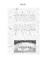
- Fig. 10C is a photographic image of an imaging result of the lens face 3 captured by a charge-coupled device (CCD) camera or the like during position measurement of the convex-shaped lens face 3 such as this. As shown in Fig. 10C , the edge of the convex-shaped lens face 3 is clear and can be accurately confirmed.
- CCD charge-coupled device
- a mold 8 is used that includes a convex-shaped transfer surface 7' adhering to the face shape of each lens face 7 and a transfer surface 2 of the surface 2.
- the convex shape of the transfer surface 7' of the lens face 7 interferes and the boundary portion between the transfer surface 7' of the lens face 7 and the transfer surface 2' of the surface 2 cannot be machined with high accuracy.
- FIG. 11C is a photographic image of an imaging result of the lens face 7 during position measurement of the concave-shaped lens face 7 such as this. As shown in Fig. 11C , the edge of the concave-shaped lens face 7 is blurred and accurate visual confirmation is difficult.
- An object of the present invention is to provide a lens array in which the edges of concave-shaped lens faces can be formed with high accuracy, and the accuracy of position measurement of the lens faces can be improved.
- a lens array according to a first aspect of the present invention is a lens array formed using a mold, the lens array including a plurality of lens faces formed in an array along a predetermined array direction on a predetermined surface of a lens array main body, in which the plurality of lens faces are concave-shaped lens faces that recess inward from the predetermined surface such that face apex portions are farther away from the predetermined surface than outer peripheral edge portions.
- the outer peripheral edge portions of the plurality of lens faces are formed in positions further toward the face apex portion side than the predetermined surface with cylindrical stepped surfaces for each lens face therebetween, the stepped surfaces of which one end is the outer peripheral edge portions and another end is a plurality of opening portions formed on the predetermined surface such as to respectively face the outer peripheral edge portions.
- the outer peripheral edge portion of the concave-shaped lens face is positioned further towards the face apex side than the predetermined surface with the stepped surface therebetween, during mold machining, a transfer portion of the outer peripheral edge portion can be machined with high accuracy using a cutter in a state in which the transfer portion projects further outward than a transfer surface of the predetermined surface. Therefore, the outer peripheral edge portion can be molded with high accuracy. As a result, during position measurement of the lens face, because the outer peripheral edge portion can be accurately confirmed, position measurement can be performed with high accuracy.
- a lens array according to a second aspect is the lens array according to the first aspect in which, further, the outer peripheral edge portions of the plurality of lens faces are formed in positions shifted toward the face apex portion side from the predetermined surface by a same distance as one another.
- the amount of shift from the predetermined surface of the outer peripheral edge portion of the lens face can be made uniform among the lens faces. Therefore, position measurement of the lens faces can be efficiently performed.
- a lens array according to a third aspect is the lens array according to the first or second aspect in which, further, a rounded shape reflecting the shape of a tip end portion of a cutter used for machining the mold is formed in the opening portion of the stepped surface for each lens face.
- a rounded shape that is difficult to avoid in mold machining can be used as a means for preventing mix-up with the opening portion during confirmation of the outer peripheral edge portion. Therefore, position measurement of the lens face can be more efficiently performed.
- the edges of concave-shaped lens faces can be formed with high accuracy, and measurement accuracy of the positions of the lens faces can be improved.
- the lens array according to the present embodiment is manufactured by a manufacturing method that uses a mold, such as an injection molding method using a resin material.
- a resin material polyetherimide, cyclic olefin resin, or the like can be selected as appropriate.
- a lens array 11 As shown in Fig. 1A , a lens array 11 according to the present embodiment include a plurality of lens faces 7, each having a circular planar shape and the same dimensions, formed in an array along a predetermined array direction (lateral direction in Fig. 1A ) on a surface 2 serving as a predetermined surface of the lens array 11 (lens array main body). In a manner similar to that of a conventional lens array shown in Fig.
- each lens face 7 is a concave-shaped lens face (concave lens face) that recesses in a surface normal direction (in other words, an optical axis OA direction) from the surface 2, such that a face apex portion (intersection between the lens face 7 and the optical axis OA) is farther away from the surface 2 than an outer peripheral edge portion 7a (edge).
- the outer peripheral edge portion 7a of each lens face 7 is formed in a position further towards the face apex portion side than the surface 2. More specifically, as shown in Fig. 1A , a cylindrical stepped surface 12 having a predetermined thickness in the optical axis OA direction is interposed between the lens face 7 and the surface 2 for each lens face 7.
- Each stepped surface 12 has the outer peripheral edge portion 7a of the lens face 7 as one end and a circular opening portion 2a, of which a plurality are formed on the surface 2 such as to respectively face the outer peripheral edge portions 7a, as the other end. In this way, the outer peripheral portion 7a of each lens face 7 is positioned further towards the face apex portion side than the surface 2 with the stepped surface 12 therebetween.
- a mold 14 is used that includes a transfer surface 12' of the stepped surface 12, in addition to a convex-shaped transfer surface 7' adhering to (inverting) the face shape of each lens face 7 and a transfer surface 2' of the surface 2.
- the transfer surface 7' of the lens face 7 has a convex shape as in a conventional mold 8 shown in Fig. 11B
- the boundary portion between the end portion of the transfer surface 7' and the transfer surface 2' of the surface 2 is not on the same plane as the transfer surface 2' of the surface 2 as was in the past.
- the boundary portion is positioned projecting further outward than the transfer surface 2' of the surface 2. Because the mold 14 such as this is structured similarly to that having a recessing portion between the transfer surfaces 7' of adjacent lens faces 7, a boundary line between the transfer surface 7' of the lens face 7 and the transfer surface 12' of the stepped surface 12, equivalent to an edge portion of the recessing portion, can be machined with high accuracy using the cutter in a manner similar to when the transfer surface 3' (recessing portion) of the convex-shaped lens face 3 shown in Fig. 10B is formed,.
- a mold machining machine is preferably used that is capable of machining the transfer surface 7' of the lens face 7, machining the transfer surface 2' of the surface 2, and machining the transfer surface 12' of the stepped surface 12 by simultaneous machining (same-step machining) by a single chuck.
- a mold machining machine such as this, a lathe turning machine or a milling machine may be used.
- the boundary line between the transfer surface 7' of the lens face 7 and the transfer surface 12' of the stepped surface 12, or in other words, the transfer portion of the outer peripheral edge portion of the lens face 7 can be machined with high accuracy. Therefore, the outer peripheral edge portion 7a of the concave-shaped lens face 7 can be molded with high accuracy using the mold 14. As a result, because the outer peripheral edge portion 7a of the lens face 7 can be accurately confirmed during position measurement of the lens face 7, position measurement can be performed with high accuracy.
- each lens face 7 is formed in a position shifted toward the face apex portion side from the surface 2 by the same distance.
- the thickness of the stepped surface 12 of the lens face 7 is the same for each lens face 7.
- the amount of shift from the surface 2 of the outer peripheral edge portion 7a of the lens face 7 can be made uniform among the lens faces 7. Therefore, position measurement of the lens faces 7 can be efficiently performed.
- an R shape (reference number R in Fig. 2 ) may be formed that reflects the shape of the tip portion of the cutter used to machine the mold 14, as shown in Fig. 2 .
- R shape reference number R in Fig. 2
- a shape that is difficult to avoid in mold machining can be allowed as the shape of the molded product.
- mix-up between the opening portion 2a and the outer peripheral edge portion 7a of the lens face 7 can be prevented with certainty. Therefore, position measurement of the lens face 7 can be performed with further efficiency.
- each lens face 7 may be a spherical surface or a non-spherical surface.
- the stepped surface 12 may be formed into a circular cylinder taking into consideration ease of design, or may be formed into a circular conical surface (tapered surface) in which the inner diameter gradually increases from the outer peripheral edge portion 7a side to the opening portion 2a side, taking into consideration releasability from the mold.
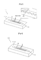
- Fig. 3 is a perspective view of a first example of the lens array 11 according to the present embodiment.
- Fig. 4 is a perspective view in which the upper portion and the lower portion in Fig. 3 are inverted.
- the overall shape of the lens array 11 of the present example is formed into a plate shape having a rectangular planar shape with a predetermined thickness in the up/down direction.
- the surface 2 on which the concave-shaped lens faces 7 are formed is formed on a recessing surface that recesses further inward than a top end surface 11a of the lens array 11 and is parallel with the top end surface 11a.
- a pair of circular through-holes 15 are formed on the surface 2 in positions on both outer sides in the array direction of the lens faces 7.
- the through-holes 15 are used for positioning a photovoltaic device (such as the VCSEL or photodetector) or an optical transmitter (such as an optical fiber or an optical waveguide) by pins provided on the photovoltatic device/optical transmitter side being inserted into the through-holes 15, when the photovoltaic device or optical transmitter is attached to the lens array 11.
- convex-shaped lens faces 3 are formed in an array, in correspondence with the concave-shaped lens faces 7, on a bottom end surface 11b of the lens array 11.
- the number of convex-shaped lens faces 3 is the same as the number of concave-shaped lens faces 7.
- the convex-shaped lens faces 3 are formed on a surface 16 that recesses further inward than the bottom end surface 11b of the lens array 11.
- the lens array 11 of the present example such as this can be used to obtain collimated light having a diameter of ⁇ 0.25mm on the outgoing side.
- the collimated light having a light-beam diameter such as this can be actualized by a position 0.15mm from the concave-shaped lens face 7 on the optical axis OA being set as an outgoing position of light towards the lens face 7, an effective diameter of the concave-shaped lens face 7 being set to ⁇ 0.06mm, an effective diameter of the convex-shaped lens face 3 being set to ⁇ 0.25mm, and an optical path length of center light within the lens array 11 (lens center thickness) being set to 0.4mm.
- a light-emitting point of the VCSEL, an end face of an optical fiber, or the like may be placed at the outgoing position of light.
- the collimated light may be received by, for example, an optical waveguide.
- the outgoing position of light towards a plane lens face 18 is required to be set at a position 0.32mm from the plane lens face 18 on the incident side on the optical axis, and the optical path length of center light within the lens array 17 is required to be set to 0.5mm.
- concave lens faces 7 is advantageous for shortening the optical path length in the device and reducing lens thickness when collimated light of a desired light-beam diameter is to be obtained.
- Fig. 7 is a cross-sectional view of a second example of the lens array 11 according to the present embodiment.
- the surface 2 on which the concave-shaped lens faces 7 are formed is formed as a recessing surface that recesses further inward than a front end face 11A of the lens array 11 and is parallel with the front end face 11A.
- a plurality of convex-shaped lens faces 3 similar to those in the first example are formed in an array on the bottom end face 11B of the lens array 11.
- a total reflection surface 19 for forming an optical path connecting each concave-shaped lens face 7 and each convex-shaped lens face 3 is formed therebetween.
- the total reflection surface 19 forms a 45° angle in relation to both the optical axis OA of the concave-shaped lens face 7 and the optical axis OA of the convex-shaped lens face 3.
- the lens array of the present example such as this can be used to obtain collimated light having a diameter of ⁇ 0.25mm on the outgoing side.
- the collimated light having a light-beam diameter such as this can be actualized by a position 0.1mm from the concave-shaped lens face 7 on the optical axis OA being set as the outgoing position of light towards the lens face 7, the effective diameter of the concave-shaped lens face 7 being set to ⁇ 0.04mm, the effective diameter of the convex-shaped lens face 3 being set to ⁇ 0.25mm, and the optical path length of center light within the lens array 11 being set to 0.85mm.
- a position 0.18mm from the plane lens face 18 on the incident side on the optical axis is required to be set as the outgoing position of light towards the lens face 18.
- concave lens faces 7 is advantageous for shortening the optical path length in the device when collimated light of a desired light-beam diameter is to be obtained.
Landscapes
- Physics & Mathematics (AREA)
- General Physics & Mathematics (AREA)
- Optics & Photonics (AREA)
- Engineering & Computer Science (AREA)
- Mechanical Engineering (AREA)
- Manufacturing & Machinery (AREA)
- Moulds For Moulding Plastics Or The Like (AREA)
- Eyeglasses (AREA)
Abstract
Description
- The present invention relates to a lens array. In particular, the present invention relates to a lens array suitable for being manufactured using a mold.
- In recent years, in reflection of the need for higher-speed communication and more compact communication devices, there has been an increasing demand for a lens array in which a plurality of lenses are arranged in parallel, as a compactly structured optical component effective for actualizing multichannel optical communication.
- This type of lens array is capable of multichannel optical transmission achieved by a plurality of light-emitting elements (such as vertical cavity surface emitting lasers [VCSEL]) and a plurality of optical fibers being optically coupled, and multichannel optical reception achieved by a plurality of optical fibers and a plurality of light-receiving elements (such as photodetectors) being optically coupled. Furthermore, in addition to usage such as this, usefulness of the lens array is expected to further rise in the field of optical communication, such as through application to optical waveguides. In accompaniment, freedom of design of the lens array is expected to further widen.
- Many of such lens arrays include convex-shaped lens faces. However, in some instances, concave-shaped lens faces are required depending on the light-beam shape to be formed, the light-beam diameter to be achieved, product dimensions, and the like (refer to, for example, Patent Literature 1).
- Patent Literature 1: Japanese Patent Laid-open Publication No.
2003-121615 - Because of its compact structure, this type of lens array is most often manufactured efficiently and at low cost by resin molding using a mold. Such trend is expected to continue.
- In instances where a lens array including concave-shaped lens faces is manufactured using a mold, a following issue attributed to the concave shape of the lens faces has been pointed out.
- In other words, in product inspection of the lens array, ordinarily, the positions of the lens faces are measured by visual confirmation of the edges (outer peripheral edge portions) of the lens faces based on a captured image of the lens faces. At this time, in the instance of a concave-shaped lens face molded using a mold, the edge may not be accurately confirmed. Here, confirmation of the edge is essential in performing position measurement of the lens face through calculation of a center point (coordinate) of the lens face based on a plurality of representative points (coordinates) on the edge. Therefore, if the edge cannot be accurately confirmed, not only does the measurement accuracy of the position of each lens face decline, variation in measurement accuracy occurs among the lens faces, resulting in a significant reduction in the advantages of using a mold, which is an efficient way to manufacture the lens array.
- The reason the edge of the concave-shaped lens face cannot be accurately confirmed in this way is because machining accuracy of the mold for molding the concave-shaped lens face is poor, and molding of the edge itself cannot be performed with high accuracy.
- This will be described in comparison with a convex-shaped lens face. First, as shown in
Fig. 10A , to mold, as alens array 1, a lens array in which a plurality of convex-shaped lens faces 3 are formed in an array on apredetermined surface 2 of the lens array, as shown inFig. 10B , amold 4 is used that includes a concave-shaped transfer surface 3' adhering to (inverting) the face shape of eachlens face 3 and a transfer surface 2' of thesurface 2. In themold 4 such as this, when machining is performed using a cutter (blade ; cutting tool) by a mold machining machine, the boundary line between the transfer surface 3' of thelens face 3 and the transfer surface 2' of thesurface 2 can be machined with high accuracy by the cutter because the transfer surface 3' of thelens face 3 has a concave shape. The boundary line appears as the edge of thelens face 3 in the molded product.Fig. 10C is a photographic image of an imaging result of thelens face 3 captured by a charge-coupled device (CCD) camera or the like during position measurement of the convex-shaped lens face 3 such as this. As shown inFig. 10C , the edge of the convex-shaped lens face 3 is clear and can be accurately confirmed. - On the other hand, as shown in
Fig. 11A , to mold, as alens array 5, a lens array in which a plurality of concave-shaped lens faces 7 are formed in an array on apredetermined surface 2 of the lens array, as shown inFig. 11B , amold 8 is used that includes a convex-shaped transfer surface 7' adhering to the face shape of eachlens face 7 and atransfer surface 2 of thesurface 2. In themold 8 such as this, during machining, the convex shape of the transfer surface 7' of thelens face 7 interferes and the boundary portion between the transfer surface 7' of thelens face 7 and the transfer surface 2' of thesurface 2 cannot be machined with high accuracy. A rounded (R) shape reflecting the shape of the tip of the cutter is formed.Fig. 11C is a photographic image of an imaging result of thelens face 7 during position measurement of the concave-shaped lens face 7 such as this. As shown inFig. 11C , the edge of the concave-shaped lens face 7 is blurred and accurate visual confirmation is difficult. - Therefore, the present invention has been achieved in light of the above-described issues. An object of the present invention is to provide a lens array in which the edges of concave-shaped lens faces can be formed with high accuracy, and the accuracy of position measurement of the lens faces can be improved.
- To achieve the above-described object, a lens array according to a first aspect of the present invention is a lens array formed using a mold, the lens array including a plurality of lens faces formed in an array along a predetermined array direction on a predetermined surface of a lens array main body, in which the plurality of lens faces are concave-shaped lens faces that recess inward from the predetermined surface such that face apex portions are farther away from the predetermined surface than outer peripheral edge portions. In the lens array, the outer peripheral edge portions of the plurality of lens faces are formed in positions further toward the face apex portion side than the predetermined surface with cylindrical stepped surfaces for each lens face therebetween, the stepped surfaces of which one end is the outer peripheral edge portions and another end is a plurality of opening portions formed on the predetermined surface such as to respectively face the outer peripheral edge portions.
- In the invention according to the first aspect, because the outer peripheral edge portion of the concave-shaped lens face is positioned further towards the face apex side than the predetermined surface with the stepped surface therebetween, during mold machining, a transfer portion of the outer peripheral edge portion can be machined with high accuracy using a cutter in a state in which the transfer portion projects further outward than a transfer surface of the predetermined surface. Therefore, the outer peripheral edge portion can be molded with high accuracy. As a result, during position measurement of the lens face, because the outer peripheral edge portion can be accurately confirmed, position measurement can be performed with high accuracy.
- In addition, a lens array according to a second aspect is the lens array according to the first aspect in which, further, the outer peripheral edge portions of the plurality of lens faces are formed in positions shifted toward the face apex portion side from the predetermined surface by a same distance as one another.
- In the invention according to the second aspect, the amount of shift from the predetermined surface of the outer peripheral edge portion of the lens face can be made uniform among the lens faces. Therefore, position measurement of the lens faces can be efficiently performed.
- Furthermore, a lens array according to a third aspect is the lens array according to the first or second aspect in which, further, a rounded shape reflecting the shape of a tip end portion of a cutter used for machining the mold is formed in the opening portion of the stepped surface for each lens face.
- In the invention according to the third aspect, a rounded shape that is difficult to avoid in mold machining can be used as a means for preventing mix-up with the opening portion during confirmation of the outer peripheral edge portion. Therefore, position measurement of the lens face can be more efficiently performed.
- In the present invention, the edges of concave-shaped lens faces can be formed with high accuracy, and measurement accuracy of the positions of the lens faces can be improved.
-
-
Fig. 1A is an overall configuration diagram of a lens array according to an embodiment of the present invention, andFig. 1B is an overall configuration diagram of a mold of the lens array according to the embodiment of the present invention corresponding toFig. 1A . -
Fig. 2 is an enlarged view of main sections of a variation example of the lens array according to the embodiment of the present invention. -
Fig. 3 is an upper perspective view of a first example of the lens array of the present invention. -
Fig. 4 is a lower perspective view ofFig. 3 . -
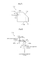
Fig. 5 is a schematic diagram of an example of an optical path actualized by the lens array inFig. 3 . -
Fig. 6 is a schematic diagram of a comparison example of the first example. -
Fig. 7 is a cross-sectional view of a second example of the lens array of the present invention; -
Fig. 8 is a schematic diagram of an example of an optical path actualized by the lens array inFig. 7 . -
Fig. 9 is a schematic diagram of a comparison example of the second example. -
Fig. 10A is an overall configuration diagram of a lens array including convex-shaped lens faces,Fig. 10B is an overall configuration diagram of a mold corresponding toFig. 10A, and Fig. 10C is a captured image of the lens face inFig. 10A . -
Fig. 11 is an explanatory diagram for explaining an issue of a conventional lens array including concave-shaped lens faces. -
- 2
- surface
- 2a
- opening portion
- 7
- lens face
- 7a
- outer peripheral edge portion
- 11
- lens array
- 12
- stepped surface
- An embodiment of a lens array of the present invention will hereinafter be described with reference to
Fig. 1 to Fig. 9 . - Sections of which the basic configuration is the same or similar to that in the past are described using the same reference numbers.
- The lens array according to the present embodiment is manufactured by a manufacturing method that uses a mold, such as an injection molding method using a resin material. As the resin material, polyetherimide, cyclic olefin resin, or the like can be selected as appropriate.
- As shown in
Fig. 1A , alens array 11 according to the present embodiment include a plurality of lens faces 7, each having a circular planar shape and the same dimensions, formed in an array along a predetermined array direction (lateral direction inFig. 1A ) on asurface 2 serving as a predetermined surface of the lens array 11 (lens array main body). In a manner similar to that of a conventional lens array shown inFig. 11A , eachlens face 7 is a concave-shaped lens face (concave lens face) that recesses in a surface normal direction (in other words, an optical axis OA direction) from thesurface 2, such that a face apex portion (intersection between thelens face 7 and the optical axis OA) is farther away from thesurface 2 than an outer peripheral edge portion 7a (edge). - However, unlike that of the conventional lens array, in the lens faces 7 according to the present embodiment, the outer peripheral edge portion 7a of each
lens face 7 is formed in a position further towards the face apex portion side than thesurface 2. More specifically, as shown inFig. 1A , a cylindrical steppedsurface 12 having a predetermined thickness in the optical axis OA direction is interposed between thelens face 7 and thesurface 2 for eachlens face 7. Each steppedsurface 12 has the outer peripheral edge portion 7a of thelens face 7 as one end and a circular opening portion 2a, of which a plurality are formed on thesurface 2 such as to respectively face the outer peripheral edge portions 7a, as the other end. In this way, the outer peripheral portion 7a of eachlens face 7 is positioned further towards the face apex portion side than thesurface 2 with the steppedsurface 12 therebetween. - To mold the
lens array 11 such as this, as shown inFig. 1B , amold 14 is used that includes a transfer surface 12' of the steppedsurface 12, in addition to a convex-shaped transfer surface 7' adhering to (inverting) the face shape of eachlens face 7 and a transfer surface 2' of thesurface 2. In themold 14 such as this, during machining using a cutter by a mold machining machine, although the transfer surface 7' of thelens face 7 has a convex shape as in aconventional mold 8 shown inFig. 11B , the boundary portion between the end portion of the transfer surface 7' and the transfer surface 2' of thesurface 2 is not on the same plane as the transfer surface 2' of thesurface 2 as was in the past. Rather, the boundary portion is positioned projecting further outward than the transfer surface 2' of thesurface 2. Because themold 14 such as this is structured similarly to that having a recessing portion between the transfer surfaces 7' of adjacent lens faces 7, a boundary line between the transfer surface 7' of thelens face 7 and the transfer surface 12' of the steppedsurface 12, equivalent to an edge portion of the recessing portion, can be machined with high accuracy using the cutter in a manner similar to when the transfer surface 3' (recessing portion) of the convex-shapedlens face 3 shown inFig. 10B is formed,. To machine themold 14 such as this, a mold machining machine is preferably used that is capable of machining the transfer surface 7' of thelens face 7, machining the transfer surface 2' of thesurface 2, and machining the transfer surface 12' of the steppedsurface 12 by simultaneous machining (same-step machining) by a single chuck. As a mold machining machine such as this, a lathe turning machine or a milling machine may be used. - In this way, according to the present embodiment, the boundary line between the transfer surface 7' of the
lens face 7 and the transfer surface 12' of the steppedsurface 12, or in other words, the transfer portion of the outer peripheral edge portion of thelens face 7 can be machined with high accuracy. Therefore, the outer peripheral edge portion 7a of the concave-shapedlens face 7 can be molded with high accuracy using themold 14. As a result, because the outer peripheral edge portion 7a of thelens face 7 can be accurately confirmed during position measurement of thelens face 7, position measurement can be performed with high accuracy. - In addition to the above-described configuration, according to the present embodiment, the outer peripheral edge portion of each
lens face 7 is formed in a position shifted toward the face apex portion side from thesurface 2 by the same distance. In other words, the thickness of the steppedsurface 12 of thelens face 7 is the same for eachlens face 7. - In the configuration such as this, the amount of shift from the
surface 2 of the outer peripheral edge portion 7a of thelens face 7 can be made uniform among the lens faces 7. Therefore, position measurement of the lens faces 7 can be efficiently performed. - In addition, in the opening portion 2a of the stepped
surface 12 of eachlens face 7, an R shape (reference number R inFig. 2 ) may be formed that reflects the shape of the tip portion of the cutter used to machine themold 14, as shown inFig. 2 . In a configuration such as this, a shape that is difficult to avoid in mold machining can be allowed as the shape of the molded product. In addition, compared to an instance in which the opening portion 2a is assumed to be formed into a sharp edge, mix-up between the opening portion 2a and the outer peripheral edge portion 7a of thelens face 7 can be prevented with certainty. Therefore, position measurement of thelens face 7 can be performed with further efficiency. - Furthermore, each
lens face 7 may be a spherical surface or a non-spherical surface. The steppedsurface 12 may be formed into a circular cylinder taking into consideration ease of design, or may be formed into a circular conical surface (tapered surface) in which the inner diameter gradually increases from the outer peripheral edge portion 7a side to the opening portion 2a side, taking into consideration releasability from the mold. - Next,
Fig. 3 is a perspective view of a first example of thelens array 11 according to the present embodiment.Fig. 4 is a perspective view in which the upper portion and the lower portion inFig. 3 are inverted. As shown inFig. 3 , the overall shape of thelens array 11 of the present example is formed into a plate shape having a rectangular planar shape with a predetermined thickness in the up/down direction. Thesurface 2 on which the concave-shaped lens faces 7 are formed is formed on a recessing surface that recesses further inward than a top end surface 11a of thelens array 11 and is parallel with the top end surface 11a. In addition, a pair of circular through-holes 15 are formed on thesurface 2 in positions on both outer sides in the array direction of the lens faces 7. The through-holes 15 are used for positioning a photovoltaic device (such as the VCSEL or photodetector) or an optical transmitter (such as an optical fiber or an optical waveguide) by pins provided on the photovoltatic device/optical transmitter side being inserted into the through-holes 15, when the photovoltaic device or optical transmitter is attached to thelens array 11. - On the other hand, as shown in
Fig. 4 , convex-shaped lens faces 3 are formed in an array, in correspondence with the concave-shaped lens faces 7, on a bottom end surface 11b of thelens array 11. The number of convex-shaped lens faces 3 is the same as the number of concave-shaped lens faces 7. The convex-shaped lens faces 3 are formed on a surface 16 that recesses further inward than the bottom end surface 11b of thelens array 11. - For example, as shown in a schematic diagram in
Fig. 5 , with the concave-shaped lens faces (non-spherical) 7 as the incident side of light and the convex-shaped lens faces (non-spherical) 3 as the outgoing side of light, thelens array 11 of the present example such as this can be used to obtain collimated light having a diameter of Φ0.25mm on the outgoing side. Specifically, the collimated light having a light-beam diameter such as this can be actualized by a position 0.15mm from the concave-shapedlens face 7 on the optical axis OA being set as an outgoing position of light towards thelens face 7, an effective diameter of the concave-shapedlens face 7 being set to Φ0.06mm, an effective diameter of the convex-shapedlens face 3 being set to Φ0.25mm, and an optical path length of center light within the lens array 11 (lens center thickness) being set to 0.4mm. A light-emitting point of the VCSEL, an end face of an optical fiber, or the like may be placed at the outgoing position of light. In addition, the collimated light may be received by, for example, an optical waveguide. - On the other hand, as shown in
Fig. 6 , in an instance in which collimated light having the same light-beam diameter as that of thelens array 11 inFig. 5 is to be obtained by a plano-convex lens array 17, the outgoing position of light towards a plane lens face 18 is required to be set at a position 0.32mm from the plane lens face 18 on the incident side on the optical axis, and the optical path length of center light within thelens array 17 is required to be set to 0.5mm. - Therefore, use of the concave lens faces 7 is advantageous for shortening the optical path length in the device and reducing lens thickness when collimated light of a desired light-beam diameter is to be obtained.
- Next,
Fig. 7 is a cross-sectional view of a second example of thelens array 11 according to the present embodiment. As shown inFig. 7 , in thelens array 11 in the present example, thesurface 2 on which the concave-shaped lens faces 7 are formed is formed as a recessing surface that recesses further inward than a front end face 11A of thelens array 11 and is parallel with the front end face 11A. In addition, a plurality of convex-shaped lens faces 3 similar to those in the first example are formed in an array on the bottom end face 11B of thelens array 11. In the present example, atotal reflection surface 19 for forming an optical path connecting each concave-shapedlens face 7 and each convex-shapedlens face 3 is formed therebetween. Thetotal reflection surface 19 forms a 45° angle in relation to both the optical axis OA of the concave-shapedlens face 7 and the optical axis OA of the convex-shapedlens face 3. - For example, as shown in
Fig. 8 , with the concave-shaped lens faces (non-spherical) 7 as the incident side of light and the convex-shaped lens faces (non-spherical) 3 as the outgoing side of light, the lens array of the present example such as this can be used to obtain collimated light having a diameter of Φ0.25mm on the outgoing side. Specifically, the collimated light having a light-beam diameter such as this can be actualized by a position 0.1mm from the concave-shapedlens face 7 on the optical axis OA being set as the outgoing position of light towards thelens face 7, the effective diameter of the concave-shapedlens face 7 being set to Φ0.04mm, the effective diameter of the convex-shapedlens face 3 being set to Φ0.25mm, and the optical path length of center light within thelens array 11 being set to 0.85mm. - On the other hand, as shown in
Fig. 9 , in an instance in which collimated light having the same light-beam diameter as that of thelens array 11 inFig. 5 is to be obtained by a plano-convex lens array 20, a position 0.18mm from the plane lens face 18 on the incident side on the optical axis is required to be set as the outgoing position of light towards the lens face 18. - Therefore, in the present example as well, use of the concave lens faces 7 is advantageous for shortening the optical path length in the device when collimated light of a desired light-beam diameter is to be obtained.
- The present invention is not limited to the above-described embodiment. Various modifications can be made without compromising the features of the present invention. For example, specific numerical values described in the examples are merely examples. Various other suitable numerical values based on concepts may, of course, be selected.
Claims (3)
- A lens array formed using a mold, the lens array comprising:a plurality of lens faces formed in an array along a predetermined array direction on a predetermined surface of a lens array main body, in which the plurality of lens faces are concave-shaped lens faces that recess inward from the predetermined surface such that face apex portions are farther away from the predetermined surface than outer peripheral edge portions, whereinthe outer peripheral edge portions of the plurality of lens faces are formed in positions further toward the face apex portion side than the predetermined surface with cylindrical stepped surfaces for each lens face therebetween, the stepped surfaces of which one end is the outer peripheral edge portions and another end is a plurality of opening portions formed on the predetermined surface such as to respectively face the outer peripheral edge portions.
- The lens array according to claim 1, wherein:the outer peripheral edge portions of the plurality of lens faces are formed in positions shifted toward the face apex portion side from the predetermined surface by a same distance as one another.
- The lens array according to claim 1 or 2, wherein:a rounded shape reflecting the shape of a tip end portion of a cutter used for machining the mold is formed in the opening portion of the stepped surface for each lens face.
Applications Claiming Priority (2)
| Application Number | Priority Date | Filing Date | Title |
|---|---|---|---|
| JP2011059516A JP2012194455A (en) | 2011-03-17 | 2011-03-17 | Lens array |
| PCT/JP2012/053914 WO2012124433A1 (en) | 2011-03-17 | 2012-02-20 | Lens array |
Publications (2)
| Publication Number | Publication Date |
|---|---|
| EP2687876A1 true EP2687876A1 (en) | 2014-01-22 |
| EP2687876A4 EP2687876A4 (en) | 2014-10-08 |
Family
ID=46830509
Family Applications (1)
| Application Number | Title | Priority Date | Filing Date |
|---|---|---|---|
| EP12757586.8A Withdrawn EP2687876A4 (en) | 2011-03-17 | 2012-02-20 | GROUPING OF LENSES |
Country Status (6)
| Country | Link |
|---|---|
| US (1) | US9007690B2 (en) |
| EP (1) | EP2687876A4 (en) |
| JP (1) | JP2012194455A (en) |
| CN (1) | CN103430057B (en) |
| TW (1) | TWI525347B (en) |
| WO (1) | WO2012124433A1 (en) |
Families Citing this family (19)
| Publication number | Priority date | Publication date | Assignee | Title |
|---|---|---|---|---|
| WO2015171597A1 (en) | 2014-05-05 | 2015-11-12 | 3D Glass Solutions, Inc. | 2d and 3d inductors antenna and transformers fabricating photoactive substrates |
| JP2017058585A (en) | 2015-09-18 | 2017-03-23 | 株式会社エンプラス | Image display body, manufacturing method thereof, and optical component |
| EP3420571A4 (en) | 2016-02-25 | 2020-03-25 | 3D Glass Solutions, Inc. | PHOTOACTIVE SUBSTRATES FOR MANUFACTURING A 3D CAPACITOR AND A CAPACITOR ARRAY |
| US12165809B2 (en) | 2016-02-25 | 2024-12-10 | 3D Glass Solutions, Inc. | 3D capacitor and capacitor array fabricating photoactive substrates |
| US11161773B2 (en) * | 2016-04-08 | 2021-11-02 | 3D Glass Solutions, Inc. | Methods of fabricating photosensitive substrates suitable for optical coupler |
| JP2018087869A (en) * | 2016-11-28 | 2018-06-07 | 株式会社エンプラス | Optical module and method for manufacturing optical module |
| WO2018200804A1 (en) | 2017-04-28 | 2018-11-01 | 3D Glass Solutions, Inc. | Rf circulator |
| CA3067812C (en) | 2017-07-07 | 2023-03-14 | 3D Glass Solutions, Inc. | 2d and 3d rf lumped element devices for rf system in a package photoactive glass substrates |
| KR102419713B1 (en) | 2017-12-15 | 2022-07-13 | 3디 글래스 솔루션즈 인코포레이티드 | Coupling Transmission Line Resonant RF Filter |
| WO2019136024A1 (en) | 2018-01-04 | 2019-07-11 | 3D Glass Solutions, Inc. | Impedance matching conductive structure for high efficiency rf circuits |
| WO2019199470A1 (en) | 2018-04-10 | 2019-10-17 | 3D Glass Solutions, Inc. | Rf integrated power condition capacitor |
| KR102475010B1 (en) | 2018-05-29 | 2022-12-07 | 3디 글래스 솔루션즈 인코포레이티드 | Low insertion loss rf transmission line |
| JP7053084B2 (en) | 2018-09-17 | 2022-04-12 | スリーディー グラス ソリューションズ,インク | Highly efficient compact slotted antenna with ground plane |
| KR102642603B1 (en) | 2018-12-28 | 2024-03-05 | 3디 글래스 솔루션즈 인코포레이티드 | Heterogenous integration for rf, microwave and mm wave systems in photoactive glass substrates |
| CA3107812C (en) | 2018-12-28 | 2023-06-27 | 3D Glass Solutions, Inc. | Annular capacitor rf, microwave and mm wave systems |
| CA3172853A1 (en) | 2019-04-05 | 2020-10-08 | 3D Glass Solutions, Inc. | Glass based empty substrate integrated waveguide devices |
| WO2020214788A1 (en) | 2019-04-18 | 2020-10-22 | 3D Glass Solutions, Inc. | High efficiency die dicing and release |
| CA3177603C (en) | 2020-04-17 | 2024-01-09 | 3D Glass Solutions, Inc. | Broadband induction |
| JP2020173448A (en) * | 2020-06-04 | 2020-10-22 | 株式会社エンプラス | Image display body, manufacturing method of the same, and optical component |
Family Cites Families (13)
| Publication number | Priority date | Publication date | Assignee | Title |
|---|---|---|---|---|
| JP3689290B2 (en) * | 1999-10-28 | 2005-08-31 | ペンタックス株式会社 | Scanning optical system |
| JP2002357701A (en) * | 2001-06-01 | 2002-12-13 | Ricoh Co Ltd | Compound scanning lens |
| JP4213897B2 (en) * | 2001-08-07 | 2009-01-21 | 株式会社日立製作所 | Method of manufacturing transfer pattern of microlens array |
| JP3999485B2 (en) | 2001-10-12 | 2007-10-31 | 日本板硝子株式会社 | Manufacturing method of optical connection module |
| JP2004323289A (en) * | 2003-04-24 | 2004-11-18 | Hitachi Maxell Ltd | Lens, lens array, lens module, lens array manufacturing method, and lens array manufacturing apparatus |
| WO2005093466A1 (en) * | 2004-03-26 | 2005-10-06 | Sony Corporation | Microlens array substrate and production method therefor |
| JP4736953B2 (en) * | 2005-06-03 | 2011-07-27 | ソニー株式会社 | Fly-eye lens sheet with light-shielding layer and method for manufacturing the same, transmissive screen, and rear projection image display device |
| CN101794005B (en) * | 2007-03-12 | 2013-12-18 | 日立电线株式会社 | Optical block reinforcing member, optical block and optical module using same |
| JP5383224B2 (en) * | 2009-01-27 | 2014-01-08 | アルプス電気株式会社 | Optical element |
| US8450821B2 (en) * | 2009-03-26 | 2013-05-28 | Micron Technology, Inc. | Method and apparatus providing combined spacer and optical lens element |
| JP2010266829A (en) * | 2009-05-18 | 2010-11-25 | Three M Innovative Properties Co | Optical member and device using the same |
| JP2011084060A (en) * | 2009-09-17 | 2011-04-28 | Fujifilm Corp | Master model of lens array and method of manufacturing the same |
| JP5896098B2 (en) * | 2010-12-09 | 2016-03-30 | 株式会社エンプラス | Lens array |
-
2011
- 2011-03-17 JP JP2011059516A patent/JP2012194455A/en active Pending
-
2012
- 2012-02-20 WO PCT/JP2012/053914 patent/WO2012124433A1/en not_active Ceased
- 2012-02-20 CN CN201280013576.0A patent/CN103430057B/en not_active Expired - Fee Related
- 2012-02-20 US US14/002,953 patent/US9007690B2/en not_active Expired - Fee Related
- 2012-02-20 EP EP12757586.8A patent/EP2687876A4/en not_active Withdrawn
- 2012-03-07 TW TW101107664A patent/TWI525347B/en not_active IP Right Cessation
Non-Patent Citations (2)
| Title |
|---|
| No further relevant documents disclosed * |
| See also references of WO2012124433A1 * |
Also Published As
| Publication number | Publication date |
|---|---|
| JP2012194455A (en) | 2012-10-11 |
| WO2012124433A1 (en) | 2012-09-20 |
| TWI525347B (en) | 2016-03-11 |
| EP2687876A4 (en) | 2014-10-08 |
| CN103430057B (en) | 2015-10-07 |
| US9007690B2 (en) | 2015-04-14 |
| US20140002906A1 (en) | 2014-01-02 |
| CN103430057A (en) | 2013-12-04 |
| TW201245773A (en) | 2012-11-16 |
Similar Documents
| Publication | Publication Date | Title |
|---|---|---|
| US9007690B2 (en) | Lens array | |
| JP5675407B2 (en) | Optical communication module and optical coupling member | |
| KR101991981B1 (en) | Optical connector having a plurality of optical fibres with staggered cleaved ends coupled to associated microlenses | |
| KR101540485B1 (en) | Duallensed unitary optical receiver assembly | |
| JP6011958B2 (en) | Optical receptacle and optical module having the same | |
| JP6289830B2 (en) | Optical receptacle and optical module | |
| EP2787379A1 (en) | Optical receptacle and optical module provided with same | |
| US8554030B2 (en) | Optically coupled device and optical module including optically coupled device | |
| JP5675408B2 (en) | Optical communication module and optical coupling member | |
| JP6461509B2 (en) | Optical receptacle and optical module | |
| EP3121631B1 (en) | Optical receptacle and optical module | |
| US20150086165A1 (en) | Optical receptacle and optical module provided with same | |
| CN104246568B (en) | Optical socket and optical module with the optical socket | |
| CN105849611B (en) | Optical receptacle and optical module | |
| CN103097921B (en) | Lens array and method for detecting lens edge thereof | |
| CN211293345U (en) | Integrated optical coupling device for high-speed parallel optical module | |
| JP5897864B2 (en) | Optical coupling member, optical connector using the same, and optical coupling member holding member | |
| JP2012237819A (en) | Holder for an optical module | |
| US9529166B2 (en) | Optical receptacle and optical module provided with same | |
| US20150078706A1 (en) | Integrated optical lens module | |
| JP2016048284A (en) | Optical receptacle and optical module | |
| JP5282988B2 (en) | Optical connector | |
| EP3418787A1 (en) | Optical system | |
| WO2022144999A1 (en) | Optical receptacle and optical module | |
| JP2012047943A (en) | Optical fiber holding member |
Legal Events
| Date | Code | Title | Description |
|---|---|---|---|
| PUAI | Public reference made under article 153(3) epc to a published international application that has entered the european phase |
Free format text: ORIGINAL CODE: 0009012 |
|
| 17P | Request for examination filed |
Effective date: 20130903 |
|
| AK | Designated contracting states |
Kind code of ref document: A1 Designated state(s): AL AT BE BG CH CY CZ DE DK EE ES FI FR GB GR HR HU IE IS IT LI LT LU LV MC MK MT NL NO PL PT RO RS SE SI SK SM TR |
|
| DAX | Request for extension of the european patent (deleted) | ||
| A4 | Supplementary search report drawn up and despatched |
Effective date: 20140904 |
|
| RIC1 | Information provided on ipc code assigned before grant |
Ipc: B29L 11/00 20060101ALI20140829BHEP Ipc: B29C 33/42 20060101ALI20140829BHEP Ipc: G02B 3/00 20060101AFI20140829BHEP |
|
| STAA | Information on the status of an ep patent application or granted ep patent |
Free format text: STATUS: EXAMINATION IS IN PROGRESS |
|
| 17Q | First examination report despatched |
Effective date: 20181119 |
|
| STAA | Information on the status of an ep patent application or granted ep patent |
Free format text: STATUS: THE APPLICATION IS DEEMED TO BE WITHDRAWN |
|
| 18D | Application deemed to be withdrawn |
Effective date: 20210901 |