EP2685308A1 - Photomixer for continous wave terahertz generation - Google Patents
Photomixer for continous wave terahertz generation Download PDFInfo
- Publication number
- EP2685308A1 EP2685308A1 EP12176226.4A EP12176226A EP2685308A1 EP 2685308 A1 EP2685308 A1 EP 2685308A1 EP 12176226 A EP12176226 A EP 12176226A EP 2685308 A1 EP2685308 A1 EP 2685308A1
- Authority
- EP
- European Patent Office
- Prior art keywords
- photomixer
- contact
- nanostructure
- nanowire
- electrode configuration
- Prior art date
- Legal status (The legal status is an assumption and is not a legal conclusion. Google has not performed a legal analysis and makes no representation as to the accuracy of the status listed.)
- Granted
Links
Images


Classifications
-
- G—PHYSICS
- G02—OPTICS
- G02F—OPTICAL DEVICES OR ARRANGEMENTS FOR THE CONTROL OF LIGHT BY MODIFICATION OF THE OPTICAL PROPERTIES OF THE MEDIA OF THE ELEMENTS INVOLVED THEREIN; NON-LINEAR OPTICS; FREQUENCY-CHANGING OF LIGHT; OPTICAL LOGIC ELEMENTS; OPTICAL ANALOGUE/DIGITAL CONVERTERS
- G02F1/00—Devices or arrangements for the control of the intensity, colour, phase, polarisation or direction of light arriving from an independent light source, e.g. switching, gating or modulating; Non-linear optics
- G02F1/35—Non-linear optics
- G02F1/353—Frequency conversion, i.e. wherein a light beam is generated with frequency components different from those of the incident light beams
- G02F1/3534—Three-wave interaction, e.g. sum-difference frequency generation
-
- H—ELECTRICITY
- H01—ELECTRIC ELEMENTS
- H01Q—ANTENNAS, i.e. RADIO AERIALS
- H01Q1/00—Details of, or arrangements associated with, antennas
- H01Q1/12—Supports; Mounting means
- H01Q1/22—Supports; Mounting means by structural association with other equipment or articles
- H01Q1/2283—Supports; Mounting means by structural association with other equipment or articles mounted in or on the surface of a semiconductor substrate as a chip-type antenna or integrated with other components into an IC package
-
- H—ELECTRICITY
- H01—ELECTRIC ELEMENTS
- H01Q—ANTENNAS, i.e. RADIO AERIALS
- H01Q9/00—Electrically-short antennas having dimensions not more than twice the operating wavelength and consisting of conductive active radiating elements
- H01Q9/005—Electrically-short antennas having dimensions not more than twice the operating wavelength and consisting of conductive active radiating elements for radiating non-sinusoidal waves
-
- G—PHYSICS
- G02—OPTICS
- G02F—OPTICAL DEVICES OR ARRANGEMENTS FOR THE CONTROL OF LIGHT BY MODIFICATION OF THE OPTICAL PROPERTIES OF THE MEDIA OF THE ELEMENTS INVOLVED THEREIN; NON-LINEAR OPTICS; FREQUENCY-CHANGING OF LIGHT; OPTICAL LOGIC ELEMENTS; OPTICAL ANALOGUE/DIGITAL CONVERTERS
- G02F2203/00—Function characteristic
- G02F2203/13—Function characteristic involving THZ radiation
Definitions
- the invention generally relates to photomixers for continuous wave terahertz generation.
- the invention relates to the using of a Nanowire for reducing the capacity between a top and bottom contact, between which a layer of photoconductive (PC) material is situated.
- the new device can additionally use the field enhancement effect in nanosized electrodes to keep the photocurrent high see reference [6] given below.
- Normal photomixers especially vertical photomixers, show a vertical layer structure or sandwich structure, where the photoconductive (PC) material is located between a first top electrode, mostly a transparent electrode, and a bottom contact.
- PC photoconductive
- THz applications is wide and fast growing field in biology, medicine, imaging, material spectroscopy, security and many other application fields.
- Photomixers are mainly used for CW THz sources.
- the classical photomixing approach is the pumping of a planar low-temperature-grown (LTG) GaAs by the laser beat signal.
- the planar photomixer can be naturally integrated to a planar antenna.
- These classical photomixers have limitations with regard to laser power, photocurrent, bias voltage, and the effective local heat dissipation [1], which cuts the THz output power.
- Another object of the invention is to improve the photomixer electrode configuration of a dc bias top contact, and a laser illuminated PC material in contact with the top contact and a bottom contact.
- the present invention solves these objects.
- the new vertical photomixer structure consists of a LTG-GaAs (also applicable for many other photoswitches grown by low-temperature grown as LTG-(In) GaAsSb, and nitrogen implanted GaAs) and sandwiched between two electrodes plates similar to [2] transferred onto a high-thermal-conductivity Si substrate (or Diamond or any other high-thermal-conductivity substrate).
- the top electrode can be an optically transparent and electrically conductive material like ITO [3] or nanowires formed into a grid structure.
- This standalone photomixer matches well with a suitable antenna to achieve the maximum THz output power.
- G is the DC photoconductance
- V 0 is the bias DC voltage
- R A is the antenna resistance
- ⁇ c the carrier life time
- C is the device capacitance.
- the device capacitance C is critical for the cut-off frequency (equation 1) and has to be designed as small as possible (at given photocurrent) to enhance the output power.
- the application of a flexible and transparent nanogrid top-electrode like nanowires, nanotubes or carbon nanotubes CNT [5] decreases the device capacitance.
- These grid electrodes can further supply photocurrents (for a given area) similar to parallel-plate configuration using the field enhancement between electrodes with Nanogap separation as shown recently in [6] .
- a new Nanogrid vertical photomixer structure was fabricated on ⁇ 500 nm thick LTG-GaAs on Si substrate similarly to ( Fig.2 ). Relatively high photocurrents of more than 0.8 mA were achieved with small dark currents of ⁇ 200 nA. A large On/Off photocurrent ratio was measured with a small Nanogrid contact on the top even for low bias voltages ⁇ 7 V (see Fig.1 ).
- the nanogrid photomixer has less effective area than vertical photomixer with parallel-plate configuration, which will strongly increase the output power according to equation 1.
- the photomixer impedance can be matched better to a resonant antenna with higher impedance than a spiral antenna.
- Fig. 1 the advantages (approx. 0.8 mA) of the nanogrid are shown.
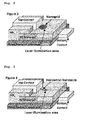
- Figure 2 shows the Nanogrid (Nanowire Grid) electrode as a top dc bias for vertical photomixer.
- the top contact connects the Nanogrid to the dc source and it is isolated from PC material by passivation layer like SiNx.
- the photomixer capacitance C is small comparing to the normal photomixer because of the small interaction area between the top Nanogrid and bottom contact.
- Nanogrid device can offer the same photocurrent I 0 like the normal vertical photomixer or even higher with less laser illumination area.
- the less capacitance C with the same photocurrent I 0 or higher generate higher THz power P( ⁇ ) according to equation 1.
- Figure 3 shows a single Nanowire horizontally connected to the PC material as a top dc bias electrode for vertical photomixer.
- the top contact connects the single Nanowire to the dc source and it is isolated from PC material by passivation layer like SiNx.
- the photomixer capacitance C is smaller comparing to the Nanogrid photomixer because of the smaller interaction area between the top Nanowire and bottom contact.
- Horizontal Nanowire device can offer the same photocurrent 10 like the Nanogrid vertical photomixer or even higher with less laser illumination area. The less capacitance C with the same photocurrent I 0 or higher generate higher THz power P( ⁇ ) according to equation 1.
- Figure 4 shows a single Nanowire tip connects by a certain angle to the PC material as a top dc bias electrode for vertical photomixer.
- the top contact connects the Nanowire to the dc source and it is isolated from PC material by passivation layer like SiNx.
- the photomixer capacitance C is much smaller comparing to the Horizontal Nanowire photomixer because of the smallest interaction area between the top Nanowire and bottom contact.
- Angled Nanowire device can offer the same photocurrent I 0 like the Horizontal Nanowire vertical photomixer or even higher with less laser illumination area.
- the less capacitance C with the same photocurrent 10 or higher generate much higher THz power P( ⁇ ) according to equation 1.
- Figure 5 shows a single Nanowire perpendicularly connected to the PC material as a top dc bias electrode for vertical photomixer.
- the top contact connects the Nanogrid to the dc source and it is isolated from PC material by passivation layer like SiNx.
- the photomixer capacitance C is the smallest value comparing to any other type above because of the smallest interaction area (it is only the Nanowire cross section area) between the top Nanowire and bottom contact.
- the Vertical Nanowire device can offer the same photocurrent 10 like any other types or even higher with much less laser illumination area.
- the smallest capacitance C with the same photocurrent 10 or higher generate very much higher THz power P( ⁇ ) according to equation 1.
- the PC Material is any photoconductive Material can be used as photoswitch for mm-Wave or THz generation or detection like LTG-GaAs, nitrogen-ion-implanted GaAs (N+iGaAs) or any other related material.
- the good heatsink substrate layer like non-conductive CVD diamond or any like Si, GaAs, etc...
- the contact area size of the used nano wire is corresponding to a diameter of around 100nm down to around 1nm, preferred are diameters from around 90 down to 10nm, and especially preferred are 80 to 60nm, and 60 down to 10nm and from 10 down to 1nm, depending of the diameter of the nanowire and on the contact angle with the PC material (see fig. 4 and 5 ).
- a nanotube (hollow nano wire) is used instead of a massive nanowire.
- the contact area with the PC material can even be reduces below the resulting contact area of ⁇ r 2 , resulting of the diameters of the nanowire dimensions named above, or even far below 1 nm 2 .
- the illumination area can be, by suitable incoupling the light into the nanotube, to the diameter of the hollow nanotube.
- the conductive nanotube or nanowire shows a light guiding element inside to deliver light to the PC material.
Landscapes
- Physics & Mathematics (AREA)
- Nonlinear Science (AREA)
- General Physics & Mathematics (AREA)
- Optics & Photonics (AREA)
- Engineering & Computer Science (AREA)
- Microelectronics & Electronic Packaging (AREA)
- Photovoltaic Devices (AREA)
- Light Receiving Elements (AREA)
Abstract
Description
- The invention generally relates to photomixers for continuous wave terahertz generation. In particular, the invention relates to the using of a Nanowire for reducing the capacity between a top and bottom contact, between which a layer of photoconductive (PC) material is situated. The new device can additionally use the field enhancement effect in nanosized electrodes to keep the photocurrent high see reference [6] given below.
- Normal photomixers, especially vertical photomixers, show a vertical layer structure or sandwich structure, where the photoconductive (PC) material is located between a first top electrode, mostly a transparent electrode, and a bottom contact.
- THz applications is wide and fast growing field in biology, medicine, imaging, material spectroscopy, security and many other application fields.
- Photomixers are mainly used for CW THz sources. The classical photomixing approach is the pumping of a planar low-temperature-grown (LTG) GaAs by the laser beat signal. The planar photomixer can be naturally integrated to a planar antenna. These classical photomixers have limitations with regard to laser power, photocurrent, bias voltage, and the effective local heat dissipation [1], which cuts the THz output power.
- It is therefore the object of the invention to suggest an improved photomixer as such and especially for the usage in combination as a CW THz sources.
- Another object of the invention is to improve the photomixer electrode configuration of a dc bias top contact, and a laser illuminated PC material in contact with the top contact and a bottom contact.
- The present invention solves these objects.
- The new vertical photomixer structure consists of a LTG-GaAs (also applicable for many other photoswitches grown by low-temperature grown as LTG-(In) GaAsSb, and nitrogen implanted GaAs) and sandwiched between two electrodes plates similar to [2] transferred onto a high-thermal-conductivity Si substrate (or Diamond or any other high-thermal-conductivity substrate). The top electrode can be an optically transparent and electrically conductive material like ITO [3] or nanowires formed into a grid structure.
- This standalone photomixer matches well with a suitable antenna to achieve the maximum THz output power. The THz power can be calculated from the simplified equation (1) given below as P(ω) [4] :

where I0 (= GV0) is the photocurrent, G is the DC photoconductance, V0 is the bias DC voltage, RA is the antenna resistance, τc is the carrier life time, and C is the device capacitance. The advantages of the vertical photomixer configuration are higher photocurrent, higher laser power due to better heat dissipation in Si substrate and increased output power. The device capacitance C is critical for the cut-off frequency (equation 1) and has to be designed as small as possible (at given photocurrent) to enhance the output power. The application of a flexible and transparent nanogrid top-electrode like nanowires, nanotubes or carbon nanotubes CNT [5] decreases the device capacitance. These grid electrodes can further supply photocurrents (for a given area) similar to parallel-plate configuration using the field enhancement between electrodes with Nanogap separation as shown recently in [6] . - A new Nanogrid vertical photomixer structure was fabricated on ∼500 nm thick LTG-GaAs on Si substrate similarly to (
Fig.2 ). Relatively high photocurrents of more than 0.8 mA were achieved with small dark currents of ∼200 nA. A large On/Off photocurrent ratio was measured with a small Nanogrid contact on the top even for low bias voltages ∼7 V (seeFig.1 ). - The potential increase in output power is large since the available power is proportional I0 2 according to the THz power equation (equation 1).
- The nanogrid photomixer has less effective area than vertical photomixer with parallel-plate configuration, which will strongly increase the output power according to equation 1. The photomixer impedance can be matched better to a resonant antenna with higher impedance than a spiral antenna.
- The present invention and its advantages and further, preferred embodiments, will become more apparent, when looking at the following description of possible embodiments of the invention, which will be described with reference to the accompanying figures, which are showing:
-
Fig. 1 : the results of measurements with the photomixer as described above; -
Fig. 2 : the design of an embodiment with a nanogrid (nanowire grid) in connection with the top contact; -
Fig. 3 : a second embodiment, using a horizontal nanowire instead of a nanogrid; -
Fig. 4 : a third embodiment, using an aligned nanowire and another configuration of contact area between the top contact and the passivation layer (here with SiNx as one of the possible materials); the passivation layer used to isolate the top contact from the PC material to avoid any additional interaction between the top and bottom contacts and that keeps the interaction only between the top Nanostructure and the bottom contact. -
Fig. 5 : a fourth, and yet preferred embodiment, using a vertical nanowire; - In
Fig. 1 the advantages (approx. 0.8 mA) of the nanogrid are shown. -
Figure 2 shows the Nanogrid (Nanowire Grid) electrode as a top dc bias for vertical photomixer. The top contact connects the Nanogrid to the dc source and it is isolated from PC material by passivation layer like SiNx. The photomixer capacitance C is small comparing to the normal photomixer because of the small interaction area between the top Nanogrid and bottom contact. Nanogrid device can offer the same photocurrent I0 like the normal vertical photomixer or even higher with less laser illumination area. The less capacitance C with the same photocurrent I0 or higher generate higher THz power P(ω) according to equation 1. -
Figure 3 shows a single Nanowire horizontally connected to the PC material as a top dc bias electrode for vertical photomixer. The top contact connects the single Nanowire to the dc source and it is isolated from PC material by passivation layer like SiNx. The photomixer capacitance C is smaller comparing to the Nanogrid photomixer because of the smaller interaction area between the top Nanowire and bottom contact. Horizontal Nanowire device can offer the same photocurrent 10 like the Nanogrid vertical photomixer or even higher with less laser illumination area. The less capacitance C with the same photocurrent I0 or higher generate higher THz power P(ω) according to equation 1. -
Figure 4 shows a single Nanowire tip connects by a certain angle to the PC material as a top dc bias electrode for vertical photomixer. The top contact connects the Nanowire to the dc source and it is isolated from PC material by passivation layer like SiNx. The photomixer capacitance C is much smaller comparing to the Horizontal Nanowire photomixer because of the smallest interaction area between the top Nanowire and bottom contact. Angled Nanowire device can offer the same photocurrent I0 like the Horizontal Nanowire vertical photomixer or even higher with less laser illumination area. The less capacitance C with the same photocurrent 10 or higher generate much higher THz power P(ω) according to equation 1. -
Figure 5 shows a single Nanowire perpendicularly connected to the PC material as a top dc bias electrode for vertical photomixer. The top contact connects the Nanogrid to the dc source and it is isolated from PC material by passivation layer like SiNx. The photomixer capacitance C is the smallest value comparing to any other type above because of the smallest interaction area (it is only the Nanowire cross section area) between the top Nanowire and bottom contact. The Vertical Nanowire device can offer the same photocurrent 10 like any other types or even higher with much less laser illumination area. The smallest capacitance C with the same photocurrent 10 or higher generate very much higher THz power P(ω) according to equation 1. - The PC Material is any photoconductive Material can be used as photoswitch for mm-Wave or THz generation or detection like LTG-GaAs, nitrogen-ion-implanted GaAs (N+iGaAs) or any other related material.
- The good heatsink substrate layer like non-conductive CVD diamond or any like Si, GaAs, etc...
- The contact area size of the used nano wire (i.e. the contact area with the PC material) is corresponding to a diameter of around 100nm down to around 1nm, preferred are diameters from around 90 down to 10nm, and especially preferred are 80 to 60nm, and 60 down to 10nm and from 10 down to 1nm, depending of the diameter of the nanowire and on the contact angle with the PC material (see
fig. 4 and 5 ). - In a further embodiment -not graphically shown in any figure-a nanotube (hollow nano wire) is used instead of a massive nanowire. With such a nanotube, for example when it is perpendicular mounted on the PC material, the contact area with the PC material can even be reduces below the resulting contact area of π r2, resulting of the diameters of the nanowire dimensions named above, or even far below 1 nm2.
- If the nanotube is fabricated with porous walls, then the illumination area can be, by suitable incoupling the light into the nanotube, to the diameter of the hollow nanotube. In yet another embodiment -not shown in any figure here- the conductive nanotube or nanowire shows a light guiding element inside to deliver light to the PC material.
-
- [1] S. Verghese, K. A. Mclntosh, and E. R. Brown. Optical and terahertz power limits in the low-temperature-grown GaAs photomixers. Phys. Lett, 71:2743-2745, 1997.Appl Phys. Lett, 71:2743-2745,
- [2] E. Peytavit, S. Arscott, D. Lippens, J. F. Lampin, L. Desplanque, F. Mollot, G. Mouret, S. Matton, P. Masselin, and R. Bocquet, Appl. Phys. Lett.81, 1174 2002.
- [3] H. Hartnagel, A. Jain, A. Dawar, and C. Jagadish, , "Semiconducting Transparent Thin Films," London: IOP publishing Ltd 1995 .
- [4] Shuji Matsuura, Hiroshi Ito, Generation of CW Terahertz Radiation with Photomixing, Topics in Applied Physics, Springer Berlin, vol 97,pp 157-204, Jan 2005.
- [5] L.Hu , Hui Wu , and Yi Cui, "Metal nanogrids, nanowires, and nanofi bers for transparent electrodes," Materials Research Society BULLETIN, vol 36 , pp. 760-765Oct. 2011.
- [6] H.Tanoto, J. Tehng, Q. Wu, M. Sun, Z.Chen, S. Maier, B.Wang, C. Chum, G. Si, A. Danner, and S. Chua,"Greatly enhanced continuous-wave terahertz emission by nanoelectrodes in a photoconductive photo mixer, Nature Photonics,.
Claims (9)
- Photomixer with a top contact, a PC material and a bottom contact, where the PC material is mounted in conductive contact with the bottom contact, characterised in that , the top contact is in conductive contact to a nanostructure, which itself is in contact with the pc material.
- Photomixer according to claim 1, characterised in that, in case of a massive nanostructure, at least the area around the nanostructure which is in conductive contact with the PC material and in case of a hollow nanostructure, at least the area within the hollow nanostructure facing the PC material is illuminated by a suitable light source.
- Photomixer according to claim 1 or 2, characterised in that , the nanostructure is a nanogridstructure or nanononwovenstructure.
- Photomixer according to claim 1 to 3, characterised in that , the nanostructure is a single nanowire.
- Photomixer according to claim 1 to 3, characterised in that , the nanostructure is a single nanowire or nanotube, which is mounted aligned between the top contact and the PC material.
- Photomixer according to claim 1 to 3, characterised in that , the nanostructure is a single nanowire or nanotube, which is mounted perpendicular on the PC material.
- An electrode configuration with a top contact and bottom contact for Photomixers with a PC material, characterised in that , the top contact, e.g. for a dc bias, is only in conductive contact to the PC material by a nanostructure made of a wire, or a tube or several wires or tubes in form of a woven or nonwoven, while the PC material is in conductive contact with the bottom contact...
- Usage of an electrode configuration according to claim 7 in any photomixing device and/or process suitable to the electrode configuration according to claims 7.
- Photomixing device or process, designed to usage the electrode configuration according to claim 7.
Priority Applications (1)
| Application Number | Priority Date | Filing Date | Title |
|---|---|---|---|
| EP12176226.4A EP2685308B1 (en) | 2012-07-12 | 2012-07-12 | Photomixer for continuous wave terahertz generation |
Applications Claiming Priority (1)
| Application Number | Priority Date | Filing Date | Title |
|---|---|---|---|
| EP12176226.4A EP2685308B1 (en) | 2012-07-12 | 2012-07-12 | Photomixer for continuous wave terahertz generation |
Publications (2)
| Publication Number | Publication Date |
|---|---|
| EP2685308A1 true EP2685308A1 (en) | 2014-01-15 |
| EP2685308B1 EP2685308B1 (en) | 2018-10-24 |
Family
ID=46727095
Family Applications (1)
| Application Number | Title | Priority Date | Filing Date |
|---|---|---|---|
| EP12176226.4A Active EP2685308B1 (en) | 2012-07-12 | 2012-07-12 | Photomixer for continuous wave terahertz generation |
Country Status (1)
| Country | Link |
|---|---|
| EP (1) | EP2685308B1 (en) |
Citations (3)
| Publication number | Priority date | Publication date | Assignee | Title |
|---|---|---|---|---|
| US20080217542A1 (en) * | 2006-03-06 | 2008-09-11 | Ravi Verma | Plasmon energy converter |
| US20080251704A1 (en) * | 2005-11-10 | 2008-10-16 | Thales | Optical Structure for Localising an Electromagnetic Field and Detector or Emitter Device Including Such a Structure |
| WO2011030011A2 (en) * | 2009-09-09 | 2011-03-17 | Centre National De La Recherche Scientifique | Light mixer for generating terahertz radiation |
-
2012
- 2012-07-12 EP EP12176226.4A patent/EP2685308B1/en active Active
Patent Citations (3)
| Publication number | Priority date | Publication date | Assignee | Title |
|---|---|---|---|---|
| US20080251704A1 (en) * | 2005-11-10 | 2008-10-16 | Thales | Optical Structure for Localising an Electromagnetic Field and Detector or Emitter Device Including Such a Structure |
| US20080217542A1 (en) * | 2006-03-06 | 2008-09-11 | Ravi Verma | Plasmon energy converter |
| WO2011030011A2 (en) * | 2009-09-09 | 2011-03-17 | Centre National De La Recherche Scientifique | Light mixer for generating terahertz radiation |
Non-Patent Citations (11)
| Title |
|---|
| APPL PHYS. LETT, vol. 71, pages 2743 - 2745 |
| CHRISTOPHER W BERRY ET AL: "Plasmonically-enhanced localization of light into photoconductive antennas", CONFERENCE ON LASERS AND ELECTRO-OPTICS (CLEO) AND QUANTUM ELECTRONICS AND LASER SCIENCE CONFERENCE (QELS), 2010 : 16 - 21 MAY 2010, SAN JOSE, CA, USA, IEEE, PISCATAWAY, NJ , USA, 16 May 2010 (2010-05-16), pages 1 - 2, XP031701242, ISBN: 978-1-55752-890-2 * |
| E. PEYTAVIT; S. ARSCOTT; D. LIPPENS; J. F. LAMPIN; L. DESPLANQUE; F. MOLLOT; G. MOURET; S. MATTON; P. MASSELIN; R. BOCQUET, APPL. PHYS. LETT., vol. 81, 2002, pages 1174 |
| H. HARTNAGEL; A. JAIN; A. DAWAR; C. JAGADISH: "Semiconducting Transparent Thin Films", 1995, LONDON: IOP PUBLISHING LTD |
| H.TANOTO; J. TEHNG; Q. WU; M. SUN; Z.CHEN; S. MAIER; B.WANG; C. CHUM; G. SI; A. DANNER: "Greatly enhanced continuous- wave terahertz emission by nanoelectrodes in a photoconductive photo mixer", NATURE PHOTONICS, vol. 6, 2012 |
| H.TANOTO; J. TEHNG; Q. WU; M. SUN; Z.CHEN; S. MAIER; B.WANG; C. CHUM; G. SI; A. DANNER: "Greatly enhanced continuous- wave terahertz emission by nanoelectrodes in a photoconductive photo mixer", NATURE PHOTONICS, vol. 6, 2012, XP002691134 * |
| L.HU; HUI WU; YI CUI: "Metal nanogrids, nanowires, and nanofi bers for transparent electrodes", MATERIALS RESEARCH SOCIETY BULLETIN, vol. 36, 2011, pages 760 - 7650 |
| LIANGBING HU ET AL: "Metal nanogrids, nanowires, and nanofibers for transparent electrodes", MRS BULLETIN, vol. 36, no. 10, 1 October 2011 (2011-10-01), pages 760 - 765, XP055051169, ISSN: 0883-7694, DOI: 10.1557/mrs.2011.234 * |
| PEYTAVIT E ET AL: "Terahertz frequency difference from vertically integrated low-temperature-grown GaAs photodetector", APPLIED PHYSICS LETTERS, AIP, AMERICAN INSTITUTE OF PHYSICS, MELVILLE, NY, US, vol. 81, no. 7, 12 August 2002 (2002-08-12), pages 1174 - 1176, XP012033217, ISSN: 0003-6951, DOI: 10.1063/1.1499517 * |
| S. VERGHESE; K. A. MCLNTOSH; E. R. BROWN: "Optical and terahertz power limits in the low-temperature-grown GaAs photomixers", PHYS. LETT, vol. 71, 1997, pages 2743 - 2745 |
| SHUJI MATSUURA; HIROSHI ITO: "Topics in Applied Physics", vol. 97, January 2005, SPRINGER BERLIN, article "Generation of CW Terahertz Radiation with Photomixing", pages: 157 - 204 |
Also Published As
| Publication number | Publication date |
|---|---|
| EP2685308B1 (en) | 2018-10-24 |
Similar Documents
| Publication | Publication Date | Title |
|---|---|---|
| Pataniya et al. | based flexible photodetector functionalized by WSe2 nanodots | |
| Zhang et al. | Ultrasensitive hybrid MoS2–ZnCdSe quantum dot photodetectors with high gain | |
| Erhard et al. | Ultrafast photodetection in the quantum wells of single AlGaAs/GaAs-based nanowires | |
| US7799988B2 (en) | Apparatus and system for a single element solar cell | |
| Shin et al. | Si–MoS2 vertical heterojunction for a photodetector with high responsivity and low noise equivalent power | |
| Binder et al. | Sub-bandgap voltage electroluminescence and magneto-oscillations in a WSe2 light-emitting van der Waals heterostructure | |
| Pospischil et al. | Solar-energy conversion and light emission in an atomic monolayer p–n diode | |
| Ross et al. | Interlayer exciton optoelectronics in a 2D heterostructure p–n junction | |
| Yan et al. | Fast, multicolor photodetection with graphene-contacted p-GaSe/n-InSe van der Waals heterostructures | |
| Wu et al. | Electrical rectifying and photosensing property of Schottky diode based on MoS2 | |
| Chen et al. | Synergistic effects of plasmonics and electron trapping in graphene short-wave infrared photodetectors with ultrahigh responsivity | |
| Deng et al. | CdS nanoscale photodetectors | |
| Jin et al. | Terahertz detectors based on carbon nanomaterials | |
| Beard et al. | Photogenerated free carrier dynamics in metal and semiconductor single-walled carbon nanotube films | |
| Zhu et al. | MXene V2CT x nanosheet/Bismuth quantum dot-based heterostructures for enhanced flexible photodetection and nonlinear photonics | |
| Long et al. | Broadband photovoltaic detectors based on an atomically thin heterostructure | |
| Jakubka et al. | Mapping charge transport by electroluminescence in chirality-selected carbon nanotube networks | |
| Taghipour et al. | Near-unity efficiency energy transfer from colloidal semiconductor quantum wells of CdSe/CdS nanoplatelets to a monolayer of MoS2 | |
| Mukherjee et al. | Solution-processed, hybrid 2D/3D MoS2/Si heterostructures with superior junction characteristics | |
| Li et al. | Solar-blind ultraviolet detection based on TiO2 nanoparticles decorated graphene field-effect transistors | |
| Zhao et al. | Electrically and optically tunable responses in graphene/transition-metal-dichalcogenide heterostructures | |
| Gabor | Impact excitation and electron–hole multiplication in graphene and carbon nanotubes | |
| Wu et al. | Efficient suppression of charge recombination in self-powered photodetectors with band-aligned transferred van der Waals metal electrodes | |
| Zhang et al. | Direct observation of charge injection of graphene in the graphene/WSe2 heterostructure by optical-pump terahertz-probe spectroscopy | |
| Xia et al. | Solution-processed gold nanorods integrated with graphene for near-infrared photodetection via hot carrier injection |
Legal Events
| Date | Code | Title | Description |
|---|---|---|---|
| PUAI | Public reference made under article 153(3) epc to a published international application that has entered the european phase |
Free format text: ORIGINAL CODE: 0009012 |
|
| AK | Designated contracting states |
Kind code of ref document: A1 Designated state(s): AL AT BE BG CH CY CZ DE DK EE ES FI FR GB GR HR HU IE IS IT LI LT LU LV MC MK MT NL NO PL PT RO RS SE SI SK SM TR |
|
| AX | Request for extension of the european patent |
Extension state: BA ME |
|
| RIN1 | Information on inventor provided before grant (corrected) |
Inventor name: AL-DAFFAIE, SHIHAB Inventor name: HARTNAGEL, HANS Inventor name: KUEPPERS, FRANKO Inventor name: YILMAZOGLU, OKTAY |
|
| RIN1 | Information on inventor provided before grant (corrected) |
Inventor name: AL-DAFFAIE, SHIHAB Inventor name: YILMAZOGLU, OKTAY Inventor name: HARTNAGEL, HANS Inventor name: KUEPPERS, FRANKO |
|
| 17P | Request for examination filed |
Effective date: 20140715 |
|
| RBV | Designated contracting states (corrected) |
Designated state(s): AL AT BE BG CH CY CZ DE DK EE ES FI FR GB GR HR HU IE IS IT LI LT LU LV MC MK MT NL NO PL PT RO RS SE SI SK SM TR |
|
| STAA | Information on the status of an ep patent application or granted ep patent |
Free format text: STATUS: EXAMINATION IS IN PROGRESS |
|
| 17Q | First examination report despatched |
Effective date: 20170811 |
|
| GRAP | Despatch of communication of intention to grant a patent |
Free format text: ORIGINAL CODE: EPIDOSNIGR1 |
|
| STAA | Information on the status of an ep patent application or granted ep patent |
Free format text: STATUS: GRANT OF PATENT IS INTENDED |
|
| INTG | Intention to grant announced |
Effective date: 20180712 |
|
| GRAS | Grant fee paid |
Free format text: ORIGINAL CODE: EPIDOSNIGR3 |
|
| GRAA | (expected) grant |
Free format text: ORIGINAL CODE: 0009210 |
|
| STAA | Information on the status of an ep patent application or granted ep patent |
Free format text: STATUS: THE PATENT HAS BEEN GRANTED |
|
| AK | Designated contracting states |
Kind code of ref document: B1 Designated state(s): AL AT BE BG CH CY CZ DE DK EE ES FI FR GB GR HR HU IE IS IT LI LT LU LV MC MK MT NL NO PL PT RO RS SE SI SK SM TR |
|
| REG | Reference to a national code |
Ref country code: GB Ref legal event code: FG4D |
|
| REG | Reference to a national code |
Ref country code: CH Ref legal event code: EP |
|
| REG | Reference to a national code |
Ref country code: IE Ref legal event code: FG4D |
|
| REG | Reference to a national code |
Ref country code: AT Ref legal event code: REF Ref document number: 1057387 Country of ref document: AT Kind code of ref document: T Effective date: 20181115 |
|
| REG | Reference to a national code |
Ref country code: DE Ref legal event code: R096 Ref document number: 602012052504 Country of ref document: DE |
|
| REG | Reference to a national code |
Ref country code: NL Ref legal event code: MP Effective date: 20181024 |
|
| REG | Reference to a national code |
Ref country code: LT Ref legal event code: MG4D |
|
| REG | Reference to a national code |
Ref country code: AT Ref legal event code: MK05 Ref document number: 1057387 Country of ref document: AT Kind code of ref document: T Effective date: 20181024 |
|
| PG25 | Lapsed in a contracting state [announced via postgrant information from national office to epo] |
Ref country code: NL Free format text: LAPSE BECAUSE OF FAILURE TO SUBMIT A TRANSLATION OF THE DESCRIPTION OR TO PAY THE FEE WITHIN THE PRESCRIBED TIME-LIMIT Effective date: 20181024 |
|
| PG25 | Lapsed in a contracting state [announced via postgrant information from national office to epo] |
Ref country code: IS Free format text: LAPSE BECAUSE OF FAILURE TO SUBMIT A TRANSLATION OF THE DESCRIPTION OR TO PAY THE FEE WITHIN THE PRESCRIBED TIME-LIMIT Effective date: 20190224 Ref country code: FI Free format text: LAPSE BECAUSE OF FAILURE TO SUBMIT A TRANSLATION OF THE DESCRIPTION OR TO PAY THE FEE WITHIN THE PRESCRIBED TIME-LIMIT Effective date: 20181024 Ref country code: AT Free format text: LAPSE BECAUSE OF FAILURE TO SUBMIT A TRANSLATION OF THE DESCRIPTION OR TO PAY THE FEE WITHIN THE PRESCRIBED TIME-LIMIT Effective date: 20181024 Ref country code: HR Free format text: LAPSE BECAUSE OF FAILURE TO SUBMIT A TRANSLATION OF THE DESCRIPTION OR TO PAY THE FEE WITHIN THE PRESCRIBED TIME-LIMIT Effective date: 20181024 Ref country code: LT Free format text: LAPSE BECAUSE OF FAILURE TO SUBMIT A TRANSLATION OF THE DESCRIPTION OR TO PAY THE FEE WITHIN THE PRESCRIBED TIME-LIMIT Effective date: 20181024 Ref country code: LV Free format text: LAPSE BECAUSE OF FAILURE TO SUBMIT A TRANSLATION OF THE DESCRIPTION OR TO PAY THE FEE WITHIN THE PRESCRIBED TIME-LIMIT Effective date: 20181024 Ref country code: NO Free format text: LAPSE BECAUSE OF FAILURE TO SUBMIT A TRANSLATION OF THE DESCRIPTION OR TO PAY THE FEE WITHIN THE PRESCRIBED TIME-LIMIT Effective date: 20190124 Ref country code: ES Free format text: LAPSE BECAUSE OF FAILURE TO SUBMIT A TRANSLATION OF THE DESCRIPTION OR TO PAY THE FEE WITHIN THE PRESCRIBED TIME-LIMIT Effective date: 20181024 Ref country code: BG Free format text: LAPSE BECAUSE OF FAILURE TO SUBMIT A TRANSLATION OF THE DESCRIPTION OR TO PAY THE FEE WITHIN THE PRESCRIBED TIME-LIMIT Effective date: 20190124 Ref country code: PL Free format text: LAPSE BECAUSE OF FAILURE TO SUBMIT A TRANSLATION OF THE DESCRIPTION OR TO PAY THE FEE WITHIN THE PRESCRIBED TIME-LIMIT Effective date: 20181024 |
|
| PG25 | Lapsed in a contracting state [announced via postgrant information from national office to epo] |
Ref country code: SE Free format text: LAPSE BECAUSE OF FAILURE TO SUBMIT A TRANSLATION OF THE DESCRIPTION OR TO PAY THE FEE WITHIN THE PRESCRIBED TIME-LIMIT Effective date: 20181024 Ref country code: AL Free format text: LAPSE BECAUSE OF FAILURE TO SUBMIT A TRANSLATION OF THE DESCRIPTION OR TO PAY THE FEE WITHIN THE PRESCRIBED TIME-LIMIT Effective date: 20181024 Ref country code: PT Free format text: LAPSE BECAUSE OF FAILURE TO SUBMIT A TRANSLATION OF THE DESCRIPTION OR TO PAY THE FEE WITHIN THE PRESCRIBED TIME-LIMIT Effective date: 20190224 Ref country code: RS Free format text: LAPSE BECAUSE OF FAILURE TO SUBMIT A TRANSLATION OF THE DESCRIPTION OR TO PAY THE FEE WITHIN THE PRESCRIBED TIME-LIMIT Effective date: 20181024 Ref country code: GR Free format text: LAPSE BECAUSE OF FAILURE TO SUBMIT A TRANSLATION OF THE DESCRIPTION OR TO PAY THE FEE WITHIN THE PRESCRIBED TIME-LIMIT Effective date: 20190125 |
|
| REG | Reference to a national code |
Ref country code: DE Ref legal event code: R097 Ref document number: 602012052504 Country of ref document: DE |
|
| PG25 | Lapsed in a contracting state [announced via postgrant information from national office to epo] |
Ref country code: CZ Free format text: LAPSE BECAUSE OF FAILURE TO SUBMIT A TRANSLATION OF THE DESCRIPTION OR TO PAY THE FEE WITHIN THE PRESCRIBED TIME-LIMIT Effective date: 20181024 Ref country code: DK Free format text: LAPSE BECAUSE OF FAILURE TO SUBMIT A TRANSLATION OF THE DESCRIPTION OR TO PAY THE FEE WITHIN THE PRESCRIBED TIME-LIMIT Effective date: 20181024 Ref country code: IT Free format text: LAPSE BECAUSE OF FAILURE TO SUBMIT A TRANSLATION OF THE DESCRIPTION OR TO PAY THE FEE WITHIN THE PRESCRIBED TIME-LIMIT Effective date: 20181024 |
|
| PG25 | Lapsed in a contracting state [announced via postgrant information from national office to epo] |
Ref country code: SM Free format text: LAPSE BECAUSE OF FAILURE TO SUBMIT A TRANSLATION OF THE DESCRIPTION OR TO PAY THE FEE WITHIN THE PRESCRIBED TIME-LIMIT Effective date: 20181024 Ref country code: RO Free format text: LAPSE BECAUSE OF FAILURE TO SUBMIT A TRANSLATION OF THE DESCRIPTION OR TO PAY THE FEE WITHIN THE PRESCRIBED TIME-LIMIT Effective date: 20181024 Ref country code: EE Free format text: LAPSE BECAUSE OF FAILURE TO SUBMIT A TRANSLATION OF THE DESCRIPTION OR TO PAY THE FEE WITHIN THE PRESCRIBED TIME-LIMIT Effective date: 20181024 Ref country code: SK Free format text: LAPSE BECAUSE OF FAILURE TO SUBMIT A TRANSLATION OF THE DESCRIPTION OR TO PAY THE FEE WITHIN THE PRESCRIBED TIME-LIMIT Effective date: 20181024 |
|
| PLBE | No opposition filed within time limit |
Free format text: ORIGINAL CODE: 0009261 |
|
| STAA | Information on the status of an ep patent application or granted ep patent |
Free format text: STATUS: NO OPPOSITION FILED WITHIN TIME LIMIT |
|
| 26N | No opposition filed |
Effective date: 20190725 |
|
| PG25 | Lapsed in a contracting state [announced via postgrant information from national office to epo] |
Ref country code: SI Free format text: LAPSE BECAUSE OF FAILURE TO SUBMIT A TRANSLATION OF THE DESCRIPTION OR TO PAY THE FEE WITHIN THE PRESCRIBED TIME-LIMIT Effective date: 20181024 |
|
| PG25 | Lapsed in a contracting state [announced via postgrant information from national office to epo] |
Ref country code: MC Free format text: LAPSE BECAUSE OF FAILURE TO SUBMIT A TRANSLATION OF THE DESCRIPTION OR TO PAY THE FEE WITHIN THE PRESCRIBED TIME-LIMIT Effective date: 20181024 |
|
| REG | Reference to a national code |
Ref country code: CH Ref legal event code: PL |
|
| PG25 | Lapsed in a contracting state [announced via postgrant information from national office to epo] |
Ref country code: TR Free format text: LAPSE BECAUSE OF FAILURE TO SUBMIT A TRANSLATION OF THE DESCRIPTION OR TO PAY THE FEE WITHIN THE PRESCRIBED TIME-LIMIT Effective date: 20181024 |
|
| REG | Reference to a national code |
Ref country code: BE Ref legal event code: MM Effective date: 20190731 |
|
| PG25 | Lapsed in a contracting state [announced via postgrant information from national office to epo] |
Ref country code: LI Free format text: LAPSE BECAUSE OF NON-PAYMENT OF DUE FEES Effective date: 20190731 Ref country code: LU Free format text: LAPSE BECAUSE OF NON-PAYMENT OF DUE FEES Effective date: 20190712 Ref country code: BE Free format text: LAPSE BECAUSE OF NON-PAYMENT OF DUE FEES Effective date: 20190731 Ref country code: CH Free format text: LAPSE BECAUSE OF NON-PAYMENT OF DUE FEES Effective date: 20190731 |
|
| PG25 | Lapsed in a contracting state [announced via postgrant information from national office to epo] |
Ref country code: IE Free format text: LAPSE BECAUSE OF NON-PAYMENT OF DUE FEES Effective date: 20190712 |
|
| PG25 | Lapsed in a contracting state [announced via postgrant information from national office to epo] |
Ref country code: CY Free format text: LAPSE BECAUSE OF FAILURE TO SUBMIT A TRANSLATION OF THE DESCRIPTION OR TO PAY THE FEE WITHIN THE PRESCRIBED TIME-LIMIT Effective date: 20181024 |
|
| PG25 | Lapsed in a contracting state [announced via postgrant information from national office to epo] |
Ref country code: MT Free format text: LAPSE BECAUSE OF FAILURE TO SUBMIT A TRANSLATION OF THE DESCRIPTION OR TO PAY THE FEE WITHIN THE PRESCRIBED TIME-LIMIT Effective date: 20181024 Ref country code: HU Free format text: LAPSE BECAUSE OF FAILURE TO SUBMIT A TRANSLATION OF THE DESCRIPTION OR TO PAY THE FEE WITHIN THE PRESCRIBED TIME-LIMIT; INVALID AB INITIO Effective date: 20120712 |
|
| PG25 | Lapsed in a contracting state [announced via postgrant information from national office to epo] |
Ref country code: MK Free format text: LAPSE BECAUSE OF FAILURE TO SUBMIT A TRANSLATION OF THE DESCRIPTION OR TO PAY THE FEE WITHIN THE PRESCRIBED TIME-LIMIT Effective date: 20181024 |
|
| PGFP | Annual fee paid to national office [announced via postgrant information from national office to epo] |
Ref country code: DE Payment date: 20250722 Year of fee payment: 14 |
|
| PGFP | Annual fee paid to national office [announced via postgrant information from national office to epo] |
Ref country code: GB Payment date: 20250724 Year of fee payment: 14 |
|
| PGFP | Annual fee paid to national office [announced via postgrant information from national office to epo] |
Ref country code: FR Payment date: 20250723 Year of fee payment: 14 |