EP2683030B1 - Wideband monopole antenna and electronic device - Google Patents
Wideband monopole antenna and electronic device Download PDFInfo
- Publication number
- EP2683030B1 EP2683030B1 EP12195242.8A EP12195242A EP2683030B1 EP 2683030 B1 EP2683030 B1 EP 2683030B1 EP 12195242 A EP12195242 A EP 12195242A EP 2683030 B1 EP2683030 B1 EP 2683030B1
- Authority
- EP
- European Patent Office
- Prior art keywords
- monopole antenna
- wideband monopole
- radiating portion
- current path
- feeding
- Prior art date
- Legal status (The legal status is an assumption and is not a legal conclusion. Google has not performed a legal analysis and makes no representation as to the accuracy of the status listed.)
- Not-in-force
Links
- 230000005404 monopole Effects 0.000 title claims description 72
- 239000000758 substrate Substances 0.000 claims description 27
- 230000005855 radiation Effects 0.000 claims description 6
- 230000008054 signal transmission Effects 0.000 claims description 5
- 238000013461 design Methods 0.000 description 10
- 239000004020 conductor Substances 0.000 description 8
- 230000005540 biological transmission Effects 0.000 description 7
- 238000005452 bending Methods 0.000 description 4
- 238000010586 diagram Methods 0.000 description 4
- 238000004891 communication Methods 0.000 description 2
- GWAOOGWHPITOEY-UHFFFAOYSA-N 1,5,2,4-dioxadithiane 2,2,4,4-tetraoxide Chemical compound O=S1(=O)CS(=O)(=O)OCO1 GWAOOGWHPITOEY-UHFFFAOYSA-N 0.000 description 1
- 230000004323 axial length Effects 0.000 description 1
- 230000000694 effects Effects 0.000 description 1
- 238000005516 engineering process Methods 0.000 description 1
- 238000011156 evaluation Methods 0.000 description 1
- 238000009413 insulation Methods 0.000 description 1
- 230000007774 longterm Effects 0.000 description 1
- 239000000463 material Substances 0.000 description 1
- 238000000034 method Methods 0.000 description 1
- 238000012986 modification Methods 0.000 description 1
- 230000004048 modification Effects 0.000 description 1
- 239000000779 smoke Substances 0.000 description 1
Images

Classifications
-
- H—ELECTRICITY
- H01—ELECTRIC ELEMENTS
- H01Q—ANTENNAS, i.e. RADIO AERIALS
- H01Q1/00—Details of, or arrangements associated with, antennas
- H01Q1/36—Structural form of radiating elements, e.g. cone, spiral, umbrella; Particular materials used therewith
- H01Q1/38—Structural form of radiating elements, e.g. cone, spiral, umbrella; Particular materials used therewith formed by a conductive layer on an insulating support
-
- H—ELECTRICITY
- H01—ELECTRIC ELEMENTS
- H01Q—ANTENNAS, i.e. RADIO AERIALS
- H01Q5/00—Arrangements for simultaneous operation of antennas on two or more different wavebands, e.g. dual-band or multi-band arrangements
- H01Q5/30—Arrangements for providing operation on different wavebands
- H01Q5/307—Individual or coupled radiating elements, each element being fed in an unspecified way
- H01Q5/342—Individual or coupled radiating elements, each element being fed in an unspecified way for different propagation modes
- H01Q5/357—Individual or coupled radiating elements, each element being fed in an unspecified way for different propagation modes using a single feed point
- H01Q5/364—Creating multiple current paths
- H01Q5/371—Branching current paths
-
- H—ELECTRICITY
- H01—ELECTRIC ELEMENTS
- H01Q—ANTENNAS, i.e. RADIO AERIALS
- H01Q9/00—Electrically-short antennas having dimensions not more than twice the operating wavelength and consisting of conductive active radiating elements
- H01Q9/04—Resonant antennas
- H01Q9/30—Resonant antennas with feed to end of elongated active element, e.g. unipole
- H01Q9/40—Element having extended radiating surface
Definitions
- the present disclosure relates to a wideband monopole antenna and electronic device in particular, to a wideband monopole antenna planarly disposed on a circuit board substrate and an electronic device thereof.
- the primary operating frequency range for the Universal Mobile Telecommunication System is from 1920MHz to 2170MHz.
- the primary operating frequency range of IEEE 802.11bg standard is from 2.40GHz to 2.50GHz
- the primary operating frequency range of Long Term Evaluation (LTE) standard is from 1.71GHz to 2.70GHz
- the primary operating frequency range of IEEE 802.11a standard is from 5.51GHz to 5.85GHz.
- the primary operating frequency range is from 3.1 GHz to 4.8GHz.
- an exemplary embodiment of the present disclosure provides a wideband monopole antenna which can be planarly placed on the surface of a substrate.
- the wideband monopole antenna can further have wider operating frequency band through configuring the width of the slots between the radiating portions and the signal ground portion.
- An exemplary embodiment of the present disclosure provides a wideband monopole antenna as defined in claim 1.
- At least a portion of the third side is parallel to the fifth side and at least a portion of the fourth side is parallel to the sixth side.
- the first radiating portion includes a first end and a second end in which the first end coupled to the feeding portion extends toward the second end and is gradually enlarged.
- the second radiating portion includes a third end and a fourth end, with the second radiating portion extends from the third end coupled to the feeding portion toward the fourth end through at least a bending portion. Accordingly, a first gap is form between the first radiating portion and the second radiating portion. The first end of the first radiating portion is adjacent to the third end while the third end of the second radiating portion is adjacent to the forth end.
- the signal ground portion is used for transmitting a data signal.
- the wideband monopole antenna at least having a first current path and a second current path. The first current path passing through the feeding portion and the first radiating portion while the second current path passing through the feeding portion and the second radiating portion to have the wideband monopole antenna emitting the data signal through at least the first current path or the second current path.
- the length of the first current path may be shorter than the second current path.
- an exemplary embodiment of the present disclosure further provides an electronic device as defined in claim 6.
- the wideband monopole antenna and the electronic device provided in the present disclosure not only may be planarly disposed on the surface of the circuit board substrate placed inside the electronic device to avoid having the antenna protruded and exposed outside the electronic device.
- the VSWR of the wideband monopole antenna in a frequency band further can satisfy the industrial standard and requirement through designing the width associated with the first and the second slots.
- FIG. 1 shows an overhead view illustrating a wideband monopole antenna provided in accordance to an exemplary embodiment of the present disclosure.
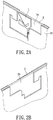
- FIG. 2A shows an isometric diagram illustrating the wideband monopole antenna provided in accordance to the exemplary embodiment of the present disclosure.
- a wideband monopole antenna 1 and a signal ground portion 20 in the instant embodiment are respectively disposed on a surface 2a of a circuit board substrate 2.
- the wideband monopole antenna 1 includes a feeding portion 10, a first radiating portion 12, and a second radiating portion 14.
- the wideband monopole antenna 1 is used for emitting the data signal transmitted by the feeding cable 24.
- the wideband monopole antenna may be an antenna for an electronic device (not shown) to provide the electronic device with the wireless transmission capability.
- the described electronic device further includes a signal transmission module (not shown) which is coupled to the feeding portion 10 of the wideband monopole antenna 1 through the feeding cable 24.
- the signal transmission module in practice may generate electric signal to the wideband monopole antenna 1 for the wideband monopole antenna 1 to transmit therefrom wirelessly. Or the wideband monopole antenna 1 may transmit the received electric signal to the signal transmission module of the electronic device via feeding cable 24.
- the circuit board substrate 2 may be a printed circuit board while the wideband monopole antenna 1 and the signal ground portion 20 may be metallic conductors comprising of identical material. Additionally for the wideband monopole antenna 1 to have better transmission quality, the wideband monopole antenna 1 may be positioned at the edge of the circuit board substrate 2 or other appreciated positions on the circuit board substrate 2.
- the described electronic device many be a handheld communication device, a laptop, a monitor, a smoke detector, a gas detector, or other appropriate electronic equipment and the present disclosure is not limited herein. Those skilled in the art should be able to design an appropriate electronic device for integrating the disclosed wideband monopole antenna 1 therein according to the needs, thus further descriptions are hereby omitted.
- the feeding portion 10 is coupled to the feeding cable 24 for receiving the data signal transmitted by the feeding cable 24.
- the feeding portion 10 at least has a side S1 and a side S2.
- the feeding cable 24 may be a coaxial cable coupled to the feeding portion 10.
- the coaxial cable may have equivalent impedance of 50 ohms and may have an inner conductor and an outer conductor. One end of the inner conductor may electrically connect to the feeding portion 10 while the other end of the inner conductor may couple to a processor (not shown) or other proper circuitry for receiving the data signal.
- the outer conductor may couple to the signal ground portion 20.
- the inner conductor and the outer conductor may further include design of insulation layer, however the present disclosure is not limited thereto.
- the feeding portion 10 shown in FIG. 1 substantially takes form of an elongated strip with the feeding cable coupled to one end thereof, however the present disclosure is not limited thereto.
- the wideband monopole antenna 1 is designed to have a place that can be connected to the feeding cable 24, the connected portion is the feeding cable 24. Accordingly, so long as the transmission frequency band of the wideband monopole antenna 1 is not affected, the feeding portion 10 can be designed into other suitable shape and the present disclosure is not limited thereto.
- the first radiating portion 12 is coupled to the feeding portion 10 so that the data signal received by the feeding portion 10 can be emitted from the first radiating portion.
- the first radiating portion 12 at least has a side S3.
- the side S3 connects to a side S1 of the feeding portion 10.
- the head-end of the first radiating portion 12 is connected to the feeding portion 10 and the tail-end of the first radiating portion 12 extends outwardly from the feeding portion 10.
- the present disclosure does not limit the shape of the first radiating portion 12.
- the first radiating proton 12 may take shape of a trapezoid, i.e., the tail-end of the first radiating portion 12 may gradually enlarge.
- the first radiating portion 12 in the instant embodiment is entirely formed on the surface of the circuit board substrate, thus does not have three-dimensional structure.
- the side S1 of the feeding portion 10, the side S3 of the first radiating portion 12, and a side S5 of the signal ground portion 20 further collectively define a region i.e., a slot A1. At least a portion of the side S3 of the first radiating portion 12 is parallel to the side S5 of the signal ground portion 20 creating a substantially fixed distance d1 therebetween. The distance d1 may be viewed as the width of the slot A1. Please note that even though the present disclosure does not place any limitations on the length of the side S5 of the signal ground portion 20, however in practice the length of the first radiating portion 12 shall be less than the length of side S5 of the signal ground portion 20 such that the signal ground portion 20 may substantially cover the first radiating portion 12.
- the second radiating portion 14 is coupled to the feeding portion 10 so that the data signal received by the feeding portion 10 may also emitted from the second radiating portion 14.
- the second radiating portion 14 at least has a side S4 which is connected to the side S2 of the feeding portion 10. It can be seen from FIG. 1 , it is not necessary for the side S4 to be a straight side, instead, the side S4 may have proper bending.
- the head-end of the second radiating portion 14 is also coupled to the feeding portion 10 while the tail-end of the second radiating portion 14 extends to the edge of the circuit board substrate 2 through a bending. Even though as shown in FIG. 1 , a side of the second radiating portion 14 is justly aligned at the edge of the circuit board substrate 2, however there present disclosure is not limited thereto.
- the present disclosure does not limit the shape of the second radiating portion 14.
- the second radiating portion 14 may comprise of a polygon, a trapezoid, a strip, or a snake-like shape having bending(s).
- the second radiating portion 14 may be entirely formed on the surface 2a of the circuit board substrate 2 thereby does not have three-dimensional structure.
- the side S4 of the second radiating portion 14 and the signal ground portion 20 may collectively define another region, i.e. a slot A2.
- the slot A2 may substantially be a rectangular region.
- the boundary of the slot A2 not only includes the second radiating portion 14 and the signal ground portion 20 but also includes the edge of the circuit board substrate 2. That is the second radiating portion 14 is aligned nearing the edge of the circuit board substrate 2 while the first radiating portion 12 is away from the edge as it has being arranged close to the center of the circuit board substrate 2.
- the length of the side S6 of the signal ground portion 20 shall be greater than or equal to the nearby axial length of the second radiating portion 14 such that the signal ground portion 20 may substantially cover the second radiating portion 14.
- the wideband monopole antenna 1 in practice may be an integrally formed structure, the present disclosure therefore only defines the outline shape of the wideband monopole antenna 1 and does not place limitations on the actual boundary among the feeding portion 10, the first radiating portion 12, and the second radiating portion 14 of the wideband monopole antenna 1.
- the wideband monopole antenna 1 at least has a first current path and the second current path enabling the wideband monopole antenna 1 emitting the data signal.
- the first current path defines a path for which current is distributed to the tail-end of the first radiating portion 12 through the feeding portion 10.
- the second current path defines a path for which current is distributed to the tail-end of the second radiating portion 14 through the feeding portion 10.
- the length of the first current path shall be less than the length of the second current path.
- the first current path may be used for emitting high frequency data signal while the second current path may be used for emitting low frequency data signal.
- the first current path is related to the shape of the first radiating portion 12 and the second current path is related to the shape of the second radiating path.
- the wideband monopole antenna 1 must maintain relatively good transmission quality over frequency ranges including 1920MHz ⁇ 2170MHz, 2.40GHz ⁇ 2.50GHz, 1.71GHz ⁇ 2.70GHz, 3.1GHz ⁇ 4.8GHz, and 5.15GHz ⁇ 5.85GHz.
- the wideband monopole antenna 1 disclosed in the instant embodiment may be also applied in the licensed band including but not limited to the US Wireless Communication Services (WCS) frequency range (2.345GHz ⁇ 2.360GHz), the Multi-point Microwave Distribution System(MMDS) or Multi-channel Multi-point Distribution System frequency range (2.50 ⁇ 2.69GHz), or the international Fixed Wireless Access (FWA) frequency range (3.4GHz ⁇ 3.7GHz).
- WCS Wireless Communication Services
- MMDS Multi-point Microwave Distribution System
- FWA international Fixed Wireless Access
- the wideband monopole antenna 1 disclosed in the instant embodiment may be also applied in the unlicensed band including but not limited to ISM frequency range (2.4000 ⁇ 2.4835GHz), Unlicensed National Information Infrastructure (U-NII) frequency range (5.15GHz ⁇ 5.35GHz, 5.725GHz ⁇ 5.825GHz).
- U-NII Unlicensed National Information Infrastructure
- the present disclosure does not limit the applicable frequency bands so long as the lower frequency limit associated with the first radiating portion 12 and the second radiating portion 14 falls within the frequency band ranging from 1.7GHz to 2GHz while the upper frequency limit associated with the first radiating portion 12 and the second radiating portion 14 falls within the frequency band ranging from 5.8GHz to 6GHz.
- those skilled in the art may flexibly design the shapes for the first radiating portion 12 and the second radiating portion 14 according to the application needs.
- the signal ground portion 20 further includes a impedance matching structure 22 which is adapted for improving the signal radiation field.
- the impedance matching structure 22 and the side S5 are interconnected.
- the impedance matching structure 22 at least has a side S7 in parallel to the side S6.
- the wideband monopole antenna 1 is arranged between the side S6 and the side S7. Accordingly the physical placement of the wideband monopole antenna 1 may be defined.
- FIG. 2B shows an isometric diagram illustrating another surface of the circuit board substrate 2 provided in accordance to the exemplary embodiment of the present disclosure.
- the signal ground portion 20 and the edge of the circuit board substrate 2 collectively surround an antenna placement region on the surface 2a.
- the wideband monopole antenna 1 thus is formed in the described antenna placement region.
- a proper design may be implemented on another surface 2b of the circuit board substrate 2b.
- the surface 2b of the circuit board substrate 2 has a clearance region arranged thereon. The clearance region is located right behind the antenna placement region.
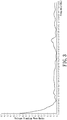
- FIG. 3 illustrates the voltage standing wave ratio (VSWR) response of the wideband monopole antenna provided in accordance to the exemplary embodiment of the present disclosure.
- the wideband monopole antenna 1 of the instant embodiment has the slot A1 and the slot A2 designed as 3mm for an example.
- the voltage standing wave ratio (VSWR) of the wideband monopole antenna 1 within frequency band ranging from 1.8GHz to 5.8GHz is less than an industry specified threshold, i.e., 2.
- an industry specified threshold i.e., 2.
- the present disclosure is not limited thereto as the threshold of the VSWR may vary according to the industry requirement.
- the wideband monopole antenna and the electronic device provided in the present disclosure not only may be planarly disposed on the surface of the circuit board substrate placed inside the electronic device to avoid having the antenna protruded and exposed outside the electronic device.
- the wideband monopole antenna may through respectively design the width of the slot between each of the two radiating portions and the signal ground portion to have the VSWR of the wideband monopole antenna within a frequency band satisfy the industrial standard and requirement.
Landscapes
- Details Of Aerials (AREA)
Description
- The present disclosure relates to a wideband monopole antenna and electronic device in particular, to a wideband monopole antenna planarly disposed on a circuit board substrate and an electronic device thereof.
- As wireless transmission technology progresses, industries have defined various transmission standards for various systems. For instance, the primary operating frequency range for the Universal Mobile Telecommunication System (UMTS) is from 1920MHz to 2170MHz. For WiFi system under IEEE 802.11 standard, in particular the primary operating frequency range of IEEE 802.11bg standard is from 2.40GHz to 2.50GHz, the primary operating frequency range of Long Term Evaluation (LTE) standard is from 1.71GHz to 2.70GHz, and the primary operating frequency range of IEEE 802.11a standard is from 5.51GHz to 5.85GHz. Additionally, according to the Ultra Wide Band (UWB) system adopting IEEE 802.15.3a standard, the primary operating frequency range is from 3.1 GHz to 4.8GHz.
- The current design trend for electronic device is geared toward light-weighed, miniaturization and compact designs. Hence, in order to effectively reduce the volume of antenna, the industry integrates the antenna inside the electronic device, increases the demands for planar and hidden antenna. However, the operating frequency band for conventional planar and hidden antenna is relatively narrow and cannot be used for different systems at same time thereby limits the applications of the associated electronic device. For example, in practice, for receiving wireless signal having lower frequency, an exposure antenna shall be used for better reception quality. But this type of antenna design certainly does not satisfy modern electronic design concept. Henceforth, how to design an antenna that can operate in a wider range while capable of being hidden inside the electronic device become the most urgent issues to be resolved. Wideband monopole antennas are disclosed in
EP 1 717 902 A1US 2005/0156783 A1 . - Accordingly, an exemplary embodiment of the present disclosure provides a wideband monopole antenna which can be planarly placed on the surface of a substrate. The wideband monopole antenna can further have wider operating frequency band through configuring the width of the slots between the radiating portions and the signal ground portion.
- An exemplary embodiment of the present disclosure provides a wideband monopole antenna as defined in
claim 1. - According to one exemplary embodiment of the present disclosure, at least a portion of the third side is parallel to the fifth side and at least a portion of the fourth side is parallel to the sixth side.
- According to one exemplary embodiment of the present disclosure, the first radiating portion includes a first end and a second end in which the first end coupled to the feeding portion extends toward the second end and is gradually enlarged. The second radiating portion includes a third end and a fourth end, with the second radiating portion extends from the third end coupled to the feeding portion toward the fourth end through at least a bending portion. Accordingly, a first gap is form between the first radiating portion and the second radiating portion. The first end of the first radiating portion is adjacent to the third end while the third end of the second radiating portion is adjacent to the forth end.
- According to one exemplary embodiment of the present disclosure, the signal ground portion is used for transmitting a data signal. The wideband monopole antenna at least having a first current path and a second current path. The first current path passing through the feeding portion and the first radiating portion while the second current path passing through the feeding portion and the second radiating portion to have the wideband monopole antenna emitting the data signal through at least the first current path or the second current path. The length of the first current path may be shorter than the second current path.
- Additionally, an exemplary embodiment of the present disclosure further provides an electronic device as defined in
claim 6. - To sum up, the wideband monopole antenna and the electronic device provided in the present disclosure not only may be planarly disposed on the surface of the circuit board substrate placed inside the electronic device to avoid having the antenna protruded and exposed outside the electronic device. The VSWR of the wideband monopole antenna in a frequency band further can satisfy the industrial standard and requirement through designing the width associated with the first and the second slots.
- In order to further understand the techniques, means and effects of the present disclosure, the following detailed descriptions and appended drawings are hereby referred, such that, through which, the purposes, features and aspects of the present disclosure can be thoroughly and concretely appreciated; however, the appended drawings are merely provided for reference and illustration, without any intention to be used for limiting the present disclosure.
- The accompanying drawings are included to provide a further understanding of the present disclosure, and are incorporated in and constitute a part of this specification. The drawings illustrate exemplary embodiments of the present disclosure and, together with the description, serve to explain the principles of the present disclosure.
-
FIG. 1 is an overhead view of a wideband monopole antenna provided in accordance to an exemplary embodiment of the present disclosure. -
FIG. 2A is an isometric diagram illustrating a wideband monopole antenna provided in accordance to an exemplary embodiment of the present disclosure. -
FIG. 2B is an isometric diagram illustrating another surface of the circuit board substrate provided in accordance to an exemplary embodiment of the present disclosure. -
FIG. 3 shows the voltage standing wave ratio (VSWR) response of a wideband monopole antenna provided in accordance to the exemplary embodiment of the present disclosure. - Reference will now be made in detail to the exemplary embodiments of the present disclosure, examples of which are illustrated in the accompanying drawings. Wherever possible, the same reference numbers are used in the drawings and the description to refer to the same or like parts.
- Please refer to
FIG. 1 andFIG. 2A at same time.FIG. 1 shows an overhead view illustrating a wideband monopole antenna provided in accordance to an exemplary embodiment of the present disclosure.FIG. 2A shows an isometric diagram illustrating the wideband monopole antenna provided in accordance to the exemplary embodiment of the present disclosure. - As shown, a
wideband monopole antenna 1 and asignal ground portion 20 in the instant embodiment are respectively disposed on asurface 2a of acircuit board substrate 2. Thewideband monopole antenna 1 includes afeeding portion 10, a first radiatingportion 12, and a second radiatingportion 14. Thewideband monopole antenna 1 is used for emitting the data signal transmitted by thefeeding cable 24. In one practical application, the wideband monopole antenna may be an antenna for an electronic device (not shown) to provide the electronic device with the wireless transmission capability. The described electronic device further includes a signal transmission module (not shown) which is coupled to thefeeding portion 10 of thewideband monopole antenna 1 through thefeeding cable 24. The signal transmission module in practice may generate electric signal to thewideband monopole antenna 1 for thewideband monopole antenna 1 to transmit therefrom wirelessly. Or thewideband monopole antenna 1 may transmit the received electric signal to the signal transmission module of the electronic device viafeeding cable 24. - In practice, the
circuit board substrate 2 may be a printed circuit board while thewideband monopole antenna 1 and thesignal ground portion 20 may be metallic conductors comprising of identical material. Additionally for thewideband monopole antenna 1 to have better transmission quality, thewideband monopole antenna 1 may be positioned at the edge of thecircuit board substrate 2 or other appreciated positions on thecircuit board substrate 2. The described electronic device many be a handheld communication device, a laptop, a monitor, a smoke detector, a gas detector, or other appropriate electronic equipment and the present disclosure is not limited herein. Those skilled in the art should be able to design an appropriate electronic device for integrating the disclosedwideband monopole antenna 1 therein according to the needs, thus further descriptions are hereby omitted. - Next detailed explanation over the correspondence between the
wideband monopole antenna 1 and thesignal ground portion 20 is provided in the subsequent paragraph. - The
feeding portion 10 is coupled to thefeeding cable 24 for receiving the data signal transmitted by thefeeding cable 24. Thefeeding portion 10 at least has a side S1 and a side S2. In practice, since the present disclosure discloses a monopole antenna and those skilled in the art should know that thefeeding portion 10 does not directly connect to thesignal ground portion 20. The feedingcable 24 may be a coaxial cable coupled to the feedingportion 10. The coaxial cable may have equivalent impedance of 50 ohms and may have an inner conductor and an outer conductor. One end of the inner conductor may electrically connect to the feedingportion 10 while the other end of the inner conductor may couple to a processor (not shown) or other proper circuitry for receiving the data signal. Moreover, the outer conductor may couple to thesignal ground portion 20. Of course, the inner conductor and the outer conductor may further include design of insulation layer, however the present disclosure is not limited thereto. - Although the feeding
portion 10 shown inFIG. 1 substantially takes form of an elongated strip with the feeding cable coupled to one end thereof, however the present disclosure is not limited thereto. In other words, as long as thewideband monopole antenna 1 is designed to have a place that can be connected to the feedingcable 24, the connected portion is the feedingcable 24. Accordingly, so long as the transmission frequency band of thewideband monopole antenna 1 is not affected, the feedingportion 10 can be designed into other suitable shape and the present disclosure is not limited thereto. - The
first radiating portion 12 is coupled to the feedingportion 10 so that the data signal received by the feedingportion 10 can be emitted from the first radiating portion. Thefirst radiating portion 12 at least has a side S3. The side S3 connects to a side S1 of the feedingportion 10. In practice, the head-end of thefirst radiating portion 12 is connected to the feedingportion 10 and the tail-end of thefirst radiating portion 12 extends outwardly from the feedingportion 10. The present disclosure does not limit the shape of thefirst radiating portion 12. For instance, thefirst radiating proton 12 may take shape of a trapezoid, i.e., the tail-end of thefirst radiating portion 12 may gradually enlarge. Moreover, thefirst radiating portion 12 in the instant embodiment is entirely formed on the surface of the circuit board substrate, thus does not have three-dimensional structure. - The side S1 of the feeding
portion 10, the side S3 of thefirst radiating portion 12, and a side S5 of thesignal ground portion 20 further collectively define a region i.e., a slot A1. At least a portion of the side S3 of thefirst radiating portion 12 is parallel to the side S5 of thesignal ground portion 20 creating a substantially fixed distance d1 therebetween. The distance d1 may be viewed as the width of the slot A1. Please note that even though the present disclosure does not place any limitations on the length of the side S5 of thesignal ground portion 20, however in practice the length of thefirst radiating portion 12 shall be less than the length of side S5 of thesignal ground portion 20 such that thesignal ground portion 20 may substantially cover thefirst radiating portion 12. - Similarly, the
second radiating portion 14 is coupled to the feedingportion 10 so that the data signal received by the feedingportion 10 may also emitted from thesecond radiating portion 14. Thesecond radiating portion 14 at least has a side S4 which is connected to the side S2 of the feedingportion 10. It can be seen fromFIG. 1 , it is not necessary for the side S4 to be a straight side, instead, the side S4 may have proper bending. In practice, the head-end of thesecond radiating portion 14 is also coupled to the feedingportion 10 while the tail-end of thesecond radiating portion 14 extends to the edge of thecircuit board substrate 2 through a bending. Even though as shown inFIG. 1 , a side of thesecond radiating portion 14 is justly aligned at the edge of thecircuit board substrate 2, however there present disclosure is not limited thereto. - In other words, the present disclosure does not limit the shape of the
second radiating portion 14. For instance, thesecond radiating portion 14 may comprise of a polygon, a trapezoid, a strip, or a snake-like shape having bending(s). Thesecond radiating portion 14 may be entirely formed on thesurface 2a of thecircuit board substrate 2 thereby does not have three-dimensional structure. - The side S4 of the
second radiating portion 14 and thesignal ground portion 20 may collectively define another region, i.e. a slot A2. In practice, the slot A2 may substantially be a rectangular region. The boundary of the slot A2 not only includes thesecond radiating portion 14 and thesignal ground portion 20 but also includes the edge of thecircuit board substrate 2. That is thesecond radiating portion 14 is aligned nearing the edge of thecircuit board substrate 2 while thefirst radiating portion 12 is away from the edge as it has being arranged close to the center of thecircuit board substrate 2. - Specifically, at least a portion of side S4 is parallel to the side S6 of the
signal ground portion 20 creating a substantially fixed distance d2 therebetween. The distance d2 may be views as the width of the slot A2. Please note that even though the present disclosure does not place any limitations on the length of the side S6 of thesignal ground portion 20, however in practice the length of the side S6 of thefirst radiating portion 12 shall be greater than or equal to the nearby axial length of thesecond radiating portion 14 such that thesignal ground portion 20 may substantially cover thesecond radiating portion 14. - The
wideband monopole antenna 1 in practice may be an integrally formed structure, the present disclosure therefore only defines the outline shape of thewideband monopole antenna 1 and does not place limitations on the actual boundary among the feedingportion 10, thefirst radiating portion 12, and thesecond radiating portion 14 of thewideband monopole antenna 1. - From data transmission perspective, the
wideband monopole antenna 1 at least has a first current path and the second current path enabling thewideband monopole antenna 1 emitting the data signal. The first current path defines a path for which current is distributed to the tail-end of thefirst radiating portion 12 through the feedingportion 10. The second current path defines a path for which current is distributed to the tail-end of thesecond radiating portion 14 through the feedingportion 10. Such that the data signal may be emitted at least through the first current path or the second path from thewideband monopole antenna 1. - In practice, the length of the first current path shall be less than the length of the second current path. Such that the first current path may be used for emitting high frequency data signal while the second current path may be used for emitting low frequency data signal. Those skilled in the art shall understand that the first current path is related to the shape of the
first radiating portion 12 and the second current path is related to the shape of the second radiating path. According, for thewideband monopole antenna 1 to be usable in UMTS system, WiFi system, UWB system, and WiMAX system, thewideband monopole antenna 1 must maintain relatively good transmission quality over frequency ranges including 1920MHz∼2170MHz, 2.40GHz∼2.50GHz, 1.71GHz∼2.70GHz, 3.1GHz∼4.8GHz, and 5.15GHz ∼5.85GHz. - The
wideband monopole antenna 1 disclosed in the instant embodiment may be also applied in the licensed band including but not limited to the US Wireless Communication Services (WCS) frequency range (2.345GHz∼2.360GHz), the Multi-point Microwave Distribution System(MMDS) or Multi-channel Multi-point Distribution System frequency range (2.50∼2.69GHz), or the international Fixed Wireless Access (FWA) frequency range (3.4GHz∼3.7GHz). Moreover, thewideband monopole antenna 1 disclosed in the instant embodiment may be also applied in the unlicensed band including but not limited to ISM frequency range (2.4000∼2.4835GHz), Unlicensed National Information Infrastructure (U-NII) frequency range (5.15GHz∼5.35GHz, 5.725GHz∼5.825GHz). - Alternatively, the present disclosure does not limit the applicable frequency bands so long as the lower frequency limit associated with the
first radiating portion 12 and thesecond radiating portion 14 falls within the frequency band ranging from 1.7GHz to 2GHz while the upper frequency limit associated with thefirst radiating portion 12 and thesecond radiating portion 14 falls within the frequency band ranging from 5.8GHz to 6GHz. Thus, those skilled in the art may flexibly design the shapes for thefirst radiating portion 12 and thesecond radiating portion 14 according to the application needs. - Please refer again to
FIG. 1 , thesignal ground portion 20 further includes aimpedance matching structure 22 which is adapted for improving the signal radiation field. It may be noted that theimpedance matching structure 22 and the side S5 are interconnected. Theimpedance matching structure 22 at least has a side S7 in parallel to the side S6. Moreover, thewideband monopole antenna 1 is arranged between the side S6 and the side S7. Accordingly the physical placement of thewideband monopole antenna 1 may be defined. - Please refer to
FIG. 2A in conjunction withFIG. 2B for viewing from another side of thecircuit board substrate 2.FIG. 2B shows an isometric diagram illustrating another surface of thecircuit board substrate 2 provided in accordance to the exemplary embodiment of the present disclosure. As shown inFIG. 2A , thesignal ground portion 20 and the edge of thecircuit board substrate 2 collectively surround an antenna placement region on thesurface 2a. Thewideband monopole antenna 1 thus is formed in the described antenna placement region. However, to enhance the radiation field associated data signal emitted by the wideband monopole antenna, a proper design may be implemented on anothersurface 2b of thecircuit board substrate 2b. For instance, thesurface 2b of thecircuit board substrate 2 has a clearance region arranged thereon. The clearance region is located right behind the antenna placement region. - For an actual implementation perspective, please refer to
FIG. 3 which illustrates the voltage standing wave ratio (VSWR) response of the wideband monopole antenna provided in accordance to the exemplary embodiment of the present disclosure. When thewideband monopole antenna 1 of the instant embodiment has the slot A1 and the slot A2 designed as 3mm for an example. As shown inFIG. 3 , the voltage standing wave ratio (VSWR) of thewideband monopole antenna 1 within frequency band ranging from 1.8GHz to 5.8GHz is less than an industry specified threshold, i.e., 2. However the present disclosure is not limited thereto as the threshold of the VSWR may vary according to the industry requirement. - In summary, the wideband monopole antenna and the electronic device provided in the present disclosure not only may be planarly disposed on the surface of the circuit board substrate placed inside the electronic device to avoid having the antenna protruded and exposed outside the electronic device. The wideband monopole antenna may through respectively design the width of the slot between each of the two radiating portions and the signal ground portion to have the VSWR of the wideband monopole antenna within a frequency band satisfy the industrial standard and requirement.
- The above-mentioned descriptions represent merely the exemplary embodiment of the present disclosure, without any intention to limit the scope of the present disclosure thereto. Various equivalent changes, alternations or modifications based on the claims of present disclosure are all consequently viewed as being embraced by the scope of the present disclosure.
Claims (10)
- A wideband monopole antenna (1), formed on a first surface (2a) of a circuit board substrate (2) with the first surface (2a) at least having a signal ground portion (20), wherein the wideband monopole antenna (1) comprises:a feeding portion (10), coupled to a feeding cable (24), the feeding portion (10) at least having a first side (S1) and a second side (S2);a first radiating portion (12), extending from a first end coupled to the feeding portion (10) to a second end, the first radiating portion (12) at least has a third side (S3), the third side (S3) being connected to the first side (S1) of the feeding portion (10), the first side (S1), the third side (S3), and the signal ground portion (20) defining a first slot (A1); anda second radiating portion (14), extending from a third end coupled to the feeding portion (10) to a fourth end, the second radiating portion (14) at least has a fourth side (S4), the fourth side (S4) of the second radiating portion (14) and the signal ground portion (20) defining a second slot (A2) therebetween;wherein the spacing between the third side (S3) of the first radiating portion (12) and a fifth side (S5) of the signal ground portion (20) in the first slot (A1) is not less than a first distance (d1) while the spacing between the fourth side (S4) of the second radiating portion (14) and a sixth side (S6) of the signal ground portion (20) in the second slot (A2) is not less than a second distance (d2) so that voltage standing wave ratio (VSWR) of the wideband monopole antenna (1) within a frequency band is less than a first threshold; further, the signal ground portion (20) further comprises an impedance matching structure (22) adapted for improving the signal radiation field, and the impedance matching structure (22) is connected to the fifth side (S5) and having a seventh side (S7) being adjacent to the second end of the first radiating portion (12) and the fourth end of the second radiating portion (14) and in parallel to the sixth side (S6);wherein, the circuit board substrate (2) has an opposite second surface (2b) in addition to the first surface (2a); and radiation field associated data signal emitted by the wideband monopole antenna (1) is enhanced since the second surface (2b) has a clearance region located opposite to the region of the wideband monopole antenna (1) on the first surface (2a) of the circuit board substrate (2); and the wideband monopole antenna (1) is arranged between the sixth side (S6) and the seventh side (S7).
- The wideband monopole antenna (1) according to claim 1, characterized in that at least a portion of the third side (S3) is parallel to the fifth side (S5) and at least a portion of the fourth side (S4) is parallel to the sixth side (S6).
- The wideband monopole antenna (1) according to claim 1, characterized in that the first radiating portion (12) extends outwardly from the feeding portion (10) and is gradually enlarged.
- The wideband monopole antenna (1) according to claim 1, characterized in that the signal ground portion (20) is used for transmitting a data signal, the wideband monopole antenna (1) at least having a first current path and a second current path, the first current path passing through the feeding portion (10) and the first radiating portion (12) while the second current path passing through the feeding portion (10) and the second radiating portion (14) to have the wideband monopole antenna (1) emitting the data signal through at least the first current path or the second current path.
- The wideband monopole antenna according to claim 4, characterized in that the length of the first current path is less than the length of the second current path.
- An electronic device, comprising:a signal transmission module, transmitting an electric signal; anda wideband monopole antenna (1)formed on a first surface (2a) of a circuit board substrate (2) with the first surface (2a) at least having a signal ground portion (20), the wideband monopole antenna (1) comprising:a feeding portion (10), coupled to the signal transmission module through a feeding cable (24) to receive the electric signal, the feeding portion (10) at least having a first side (S1) and a second side (S2);a first radiating portion (12), extending from a first end coupled to the feeding portion (10) to a second end, the first radiating portion (12) at least has a third side (S3), the third side (S3) being connected to the first side (S1) of the feeding portion (10), the first side (S1), the third side (S3), and the signal ground portion (2) defining a first slot (A1); anda second radiating portion (14), extending from a third end coupled to the feeding portion (10) to a fourth end, the second radiating portion (14) at least has a fourth side (S4), the fourth side (S4) of the second radiating portion (14) and the signal ground portion (2) defining a second slot (A2) therebetween;wherein the spacing between the third side (S3) of the first radiating portion (12) and a fifth side (S5) of the signal ground portion (2) in the first slot (A1) is not less than a first distance (d1) while the spacing between the fourth side (S4) of the second radiating portion (14) and a sixth side (S6) of the signal ground portion (2) in the second slot (A2) is not less than a second distance (d2) so that voltage standing wave ratio (VSWR) of the wideband monopole antenna (1) within a frequency band is less than a first threshold; further, the signal ground portion (2) further comprises an impedance matching structure (22) adapted for improving the signal radiation field, and the impedance matching structure (22) is connected to the fifth side (S5) and having a seventh side (S7) being adjacent to the the second end of the first radiating portion (12) and the fourth end of the second radiating portion (14) and in parallel to the sixth side (S6);wherein, the circuit board substrate (2) has an opposite second surface (2b) in addition to the first surface (2a); and radiation field associated data signal emitted by the wideband monopole antenna (1) is enhanced since the second surface (2b) has a clearance region located opposite to the region of the wideband monopole antenna (1) on the first surface (2a) of the circuit board substrate (2); and the wideband monopole antenna (1) is arranged between the sixth side (S6) and the seventh side (S7).
- The electronic device according to claim 6, wherein at least a portion of the third side (S3) is parallel to the fifth side (S5) and at least a portion of the fourth side (S4) is parallel to the sixth side (S6).
- The electronic device according to claim 6, wherein the first radiating portion (12) extends outwardly from the feeding portion (10) and is gradually enlarged.
- The electronic device according to claim 6, wherein the signal ground portion (20) is used for transmitting a data signal, the wideband monopole antenna (1) at least having a first current path and a second current path, the first current path passing through the feeding portion (10) and the first radiating portion (12) while the second current path passing through the feeding portion (10) and the second radiating portion (14) to have the wideband monopole antenna (1) emitting the data signal through at least the first current path or the second current path.
- The electronic device according to claim 9, wherein the length of the first current path is less than the length of the second current path.
Applications Claiming Priority (1)
| Application Number | Priority Date | Filing Date | Title |
|---|---|---|---|
| TW101124127A TWI508378B (en) | 2012-07-04 | 2012-07-04 | Wide band monopole antenna and electrical device |
Publications (2)
| Publication Number | Publication Date |
|---|---|
| EP2683030A1 EP2683030A1 (en) | 2014-01-08 |
| EP2683030B1 true EP2683030B1 (en) | 2017-04-26 |
Family
ID=47522297
Family Applications (1)
| Application Number | Title | Priority Date | Filing Date |
|---|---|---|---|
| EP12195242.8A Not-in-force EP2683030B1 (en) | 2012-07-04 | 2012-12-03 | Wideband monopole antenna and electronic device |
Country Status (3)
| Country | Link |
|---|---|
| US (1) | US20140009359A1 (en) |
| EP (1) | EP2683030B1 (en) |
| TW (1) | TWI508378B (en) |
Families Citing this family (11)
| Publication number | Priority date | Publication date | Assignee | Title |
|---|---|---|---|---|
| TWI509892B (en) * | 2013-03-21 | 2015-11-21 | Arcadyan Technology Corp | Antenna structure and the manufacturing method thereof |
| TWI532252B (en) * | 2014-12-24 | 2016-05-01 | 智易科技股份有限公司 | Antenna structure with cable grounding area |
| TWI560947B (en) * | 2015-02-06 | 2016-12-01 | Arcadyan Technology Corp | Dual-band dipole antenna |
| DE202015001972U1 (en) | 2015-03-09 | 2016-03-10 | Sputnik24 Communication Systems GmbH | Multifunction antenna system with RADAR reflector |
| TWI563734B (en) * | 2015-07-07 | 2016-12-21 | Arcadyan Technology Corp | Printed multi-band antenna |
| CN105226379A (en) * | 2015-08-25 | 2016-01-06 | 中国航空无线电电子研究所 | A kind of miniaturization broadband micro-strip array antenna |
| CN105071032A (en) * | 2015-08-25 | 2015-11-18 | 中国航空无线电电子研究所 | Miniaturization broadband microstrip antenna |
| WO2017061961A1 (en) * | 2015-10-08 | 2017-04-13 | Arcelik Anonim Sirketi | A communication means and the household appliance wherein the same is used |
| TWI628857B (en) * | 2016-10-06 | 2018-07-01 | 和碩聯合科技股份有限公司 | Antenna system |
| CN110571518B (en) * | 2019-09-18 | 2023-05-02 | 湖南智领通信科技有限公司 | Unmanned aerial vehicle airborne antenna based on thermoplastic polyimide board |
| CN113764885B (en) * | 2020-06-05 | 2022-12-30 | 华为技术有限公司 | Electronic device |
Citations (1)
| Publication number | Priority date | Publication date | Assignee | Title |
|---|---|---|---|---|
| US20060050002A1 (en) * | 2003-08-08 | 2006-03-09 | Chien-Jen Wang | Miniaturized cpw-fed slot antenna with dual-frequency operation |
Family Cites Families (10)
| Publication number | Priority date | Publication date | Assignee | Title |
|---|---|---|---|---|
| JP2004201278A (en) * | 2002-12-06 | 2004-07-15 | Sharp Corp | Pattern antenna |
| US20040108955A1 (en) * | 2002-12-10 | 2004-06-10 | Peter Sjoblom | Multiband antenna |
| TWI268009B (en) * | 2003-05-16 | 2006-12-01 | Hon Hai Prec Ind Co Ltd | Dual band antenna and method for making the same |
| TWI239679B (en) * | 2004-01-20 | 2005-09-11 | Micro Star Int Co Ltd | Dual-band antenna |
| JP4149974B2 (en) * | 2004-08-26 | 2008-09-17 | オムロン株式会社 | Chip antenna |
| CN1855625A (en) * | 2005-04-20 | 2006-11-01 | 启碁科技股份有限公司 | Planar monopole antenna |
| US7855686B2 (en) * | 2005-08-17 | 2010-12-21 | Agency For Science, Technology And Research | Compact antennas for ultra-wideband applications |
| TW200822454A (en) * | 2006-11-09 | 2008-05-16 | Arcadyan Technology Corp | Dual band printed antenna and dual band printed antenna module |
| JP2011061758A (en) * | 2009-08-10 | 2011-03-24 | Fujitsu Component Ltd | Antenna device |
| TWI487201B (en) * | 2012-02-10 | 2015-06-01 | Wistron Neweb Corp | Wideband antenna |
-
2012
- 2012-07-04 TW TW101124127A patent/TWI508378B/en active
- 2012-11-04 US US13/668,281 patent/US20140009359A1/en not_active Abandoned
- 2012-12-03 EP EP12195242.8A patent/EP2683030B1/en not_active Not-in-force
Patent Citations (1)
| Publication number | Priority date | Publication date | Assignee | Title |
|---|---|---|---|---|
| US20060050002A1 (en) * | 2003-08-08 | 2006-03-09 | Chien-Jen Wang | Miniaturized cpw-fed slot antenna with dual-frequency operation |
Also Published As
| Publication number | Publication date |
|---|---|
| TWI508378B (en) | 2015-11-11 |
| US20140009359A1 (en) | 2014-01-09 |
| EP2683030A1 (en) | 2014-01-08 |
| TW201403949A (en) | 2014-01-16 |
Similar Documents
| Publication | Publication Date | Title |
|---|---|---|
| EP2683030A1 (en) | Wideband monopole antenna and electronic device | |
| US7271779B2 (en) | Method, system and apparatus for an antenna | |
| TWI568076B (en) | Antenna structure | |
| US8531340B2 (en) | Multi-band antenna module | |
| US9923263B2 (en) | Mobile device | |
| US9825366B2 (en) | Printed circuit board antenna and printed circuit board | |
| CN112886194B (en) | Antenna structure | |
| US20040090374A1 (en) | Multi-band antenna | |
| TWI712218B (en) | Antenna structure | |
| CN112864609B (en) | antenna structure | |
| CN112736419B (en) | Antenna system | |
| US11699848B2 (en) | Mobile device | |
| TW201834312A (en) | Mobile device | |
| CN109728439A (en) | mobile device | |
| CN112397888B (en) | mobile device | |
| US9281565B2 (en) | Multi-frequency antenna | |
| CN101378144B (en) | Radio apparatus and antenna thereof | |
| US8373601B2 (en) | Multi-band antenna | |
| CN114389020A (en) | Antenna structure | |
| CN111478016A (en) | Mobile device | |
| US8723754B2 (en) | Multi-band antenna | |
| EP2063487A1 (en) | Dual band antenna | |
| CN113131184B (en) | Mobile device | |
| CN103545605B (en) | Broadband Monopole Antenna and Electronics | |
| CN101093912B (en) | planar antenna structure |
Legal Events
| Date | Code | Title | Description |
|---|---|---|---|
| PUAI | Public reference made under article 153(3) epc to a published international application that has entered the european phase |
Free format text: ORIGINAL CODE: 0009012 |
|
| AK | Designated contracting states |
Kind code of ref document: A1 Designated state(s): AL AT BE BG CH CY CZ DE DK EE ES FI FR GB GR HR HU IE IS IT LI LT LU LV MC MK MT NL NO PL PT RO RS SE SI SK SM TR |
|
| AX | Request for extension of the european patent |
Extension state: BA ME |
|
| 17P | Request for examination filed |
Effective date: 20140331 |
|
| RBV | Designated contracting states (corrected) |
Designated state(s): AL AT BE BG CH CY CZ DE DK EE ES FI FR GB GR HR HU IE IS IT LI LT LU LV MC MK MT NL NO PL PT RO RS SE SI SK SM TR |
|
| 17Q | First examination report despatched |
Effective date: 20160704 |
|
| GRAP | Despatch of communication of intention to grant a patent |
Free format text: ORIGINAL CODE: EPIDOSNIGR1 |
|
| INTG | Intention to grant announced |
Effective date: 20161123 |
|
| GRAS | Grant fee paid |
Free format text: ORIGINAL CODE: EPIDOSNIGR3 |
|
| GRAA | (expected) grant |
Free format text: ORIGINAL CODE: 0009210 |
|
| AK | Designated contracting states |
Kind code of ref document: B1 Designated state(s): AL AT BE BG CH CY CZ DE DK EE ES FI FR GB GR HR HU IE IS IT LI LT LU LV MC MK MT NL NO PL PT RO RS SE SI SK SM TR |
|
| REG | Reference to a national code |
Ref country code: GB Ref legal event code: FG4D |
|
| REG | Reference to a national code |
Ref country code: CH Ref legal event code: EP |
|
| REG | Reference to a national code |
Ref country code: AT Ref legal event code: REF Ref document number: 888602 Country of ref document: AT Kind code of ref document: T Effective date: 20170515 |
|
| REG | Reference to a national code |
Ref country code: IE Ref legal event code: FG4D |
|
| REG | Reference to a national code |
Ref country code: DE Ref legal event code: R096 Ref document number: 602012031570 Country of ref document: DE |
|
| REG | Reference to a national code |
Ref country code: NL Ref legal event code: MP Effective date: 20170426 |
|
| REG | Reference to a national code |
Ref country code: LT Ref legal event code: MG4D |
|
| REG | Reference to a national code |
Ref country code: AT Ref legal event code: MK05 Ref document number: 888602 Country of ref document: AT Kind code of ref document: T Effective date: 20170426 |
|
| PG25 | Lapsed in a contracting state [announced via postgrant information from national office to epo] |
Ref country code: NL Free format text: LAPSE BECAUSE OF FAILURE TO SUBMIT A TRANSLATION OF THE DESCRIPTION OR TO PAY THE FEE WITHIN THE PRESCRIBED TIME-LIMIT Effective date: 20170426 |
|
| PG25 | Lapsed in a contracting state [announced via postgrant information from national office to epo] |
Ref country code: AT Free format text: LAPSE BECAUSE OF FAILURE TO SUBMIT A TRANSLATION OF THE DESCRIPTION OR TO PAY THE FEE WITHIN THE PRESCRIBED TIME-LIMIT Effective date: 20170426 Ref country code: HR Free format text: LAPSE BECAUSE OF FAILURE TO SUBMIT A TRANSLATION OF THE DESCRIPTION OR TO PAY THE FEE WITHIN THE PRESCRIBED TIME-LIMIT Effective date: 20170426 Ref country code: LT Free format text: LAPSE BECAUSE OF FAILURE TO SUBMIT A TRANSLATION OF THE DESCRIPTION OR TO PAY THE FEE WITHIN THE PRESCRIBED TIME-LIMIT Effective date: 20170426 Ref country code: GR Free format text: LAPSE BECAUSE OF FAILURE TO SUBMIT A TRANSLATION OF THE DESCRIPTION OR TO PAY THE FEE WITHIN THE PRESCRIBED TIME-LIMIT Effective date: 20170727 Ref country code: NO Free format text: LAPSE BECAUSE OF FAILURE TO SUBMIT A TRANSLATION OF THE DESCRIPTION OR TO PAY THE FEE WITHIN THE PRESCRIBED TIME-LIMIT Effective date: 20170726 Ref country code: FI Free format text: LAPSE BECAUSE OF FAILURE TO SUBMIT A TRANSLATION OF THE DESCRIPTION OR TO PAY THE FEE WITHIN THE PRESCRIBED TIME-LIMIT Effective date: 20170426 Ref country code: ES Free format text: LAPSE BECAUSE OF FAILURE TO SUBMIT A TRANSLATION OF THE DESCRIPTION OR TO PAY THE FEE WITHIN THE PRESCRIBED TIME-LIMIT Effective date: 20170426 |
|
| PG25 | Lapsed in a contracting state [announced via postgrant information from national office to epo] |
Ref country code: LV Free format text: LAPSE BECAUSE OF FAILURE TO SUBMIT A TRANSLATION OF THE DESCRIPTION OR TO PAY THE FEE WITHIN THE PRESCRIBED TIME-LIMIT Effective date: 20170426 Ref country code: BG Free format text: LAPSE BECAUSE OF FAILURE TO SUBMIT A TRANSLATION OF THE DESCRIPTION OR TO PAY THE FEE WITHIN THE PRESCRIBED TIME-LIMIT Effective date: 20170726 Ref country code: IS Free format text: LAPSE BECAUSE OF FAILURE TO SUBMIT A TRANSLATION OF THE DESCRIPTION OR TO PAY THE FEE WITHIN THE PRESCRIBED TIME-LIMIT Effective date: 20170826 Ref country code: RS Free format text: LAPSE BECAUSE OF FAILURE TO SUBMIT A TRANSLATION OF THE DESCRIPTION OR TO PAY THE FEE WITHIN THE PRESCRIBED TIME-LIMIT Effective date: 20170426 Ref country code: SE Free format text: LAPSE BECAUSE OF FAILURE TO SUBMIT A TRANSLATION OF THE DESCRIPTION OR TO PAY THE FEE WITHIN THE PRESCRIBED TIME-LIMIT Effective date: 20170426 Ref country code: PL Free format text: LAPSE BECAUSE OF FAILURE TO SUBMIT A TRANSLATION OF THE DESCRIPTION OR TO PAY THE FEE WITHIN THE PRESCRIBED TIME-LIMIT Effective date: 20170426 |
|
| REG | Reference to a national code |
Ref country code: DE Ref legal event code: R097 Ref document number: 602012031570 Country of ref document: DE |
|
| PG25 | Lapsed in a contracting state [announced via postgrant information from national office to epo] |
Ref country code: DK Free format text: LAPSE BECAUSE OF FAILURE TO SUBMIT A TRANSLATION OF THE DESCRIPTION OR TO PAY THE FEE WITHIN THE PRESCRIBED TIME-LIMIT Effective date: 20170426 Ref country code: CZ Free format text: LAPSE BECAUSE OF FAILURE TO SUBMIT A TRANSLATION OF THE DESCRIPTION OR TO PAY THE FEE WITHIN THE PRESCRIBED TIME-LIMIT Effective date: 20170426 Ref country code: RO Free format text: LAPSE BECAUSE OF FAILURE TO SUBMIT A TRANSLATION OF THE DESCRIPTION OR TO PAY THE FEE WITHIN THE PRESCRIBED TIME-LIMIT Effective date: 20170426 Ref country code: EE Free format text: LAPSE BECAUSE OF FAILURE TO SUBMIT A TRANSLATION OF THE DESCRIPTION OR TO PAY THE FEE WITHIN THE PRESCRIBED TIME-LIMIT Effective date: 20170426 Ref country code: SK Free format text: LAPSE BECAUSE OF FAILURE TO SUBMIT A TRANSLATION OF THE DESCRIPTION OR TO PAY THE FEE WITHIN THE PRESCRIBED TIME-LIMIT Effective date: 20170426 |
|
| PG25 | Lapsed in a contracting state [announced via postgrant information from national office to epo] |
Ref country code: SM Free format text: LAPSE BECAUSE OF FAILURE TO SUBMIT A TRANSLATION OF THE DESCRIPTION OR TO PAY THE FEE WITHIN THE PRESCRIBED TIME-LIMIT Effective date: 20170426 Ref country code: IT Free format text: LAPSE BECAUSE OF FAILURE TO SUBMIT A TRANSLATION OF THE DESCRIPTION OR TO PAY THE FEE WITHIN THE PRESCRIBED TIME-LIMIT Effective date: 20170426 |
|
| PLBE | No opposition filed within time limit |
Free format text: ORIGINAL CODE: 0009261 |
|
| STAA | Information on the status of an ep patent application or granted ep patent |
Free format text: STATUS: NO OPPOSITION FILED WITHIN TIME LIMIT |
|
| 26N | No opposition filed |
Effective date: 20180129 |
|
| PG25 | Lapsed in a contracting state [announced via postgrant information from national office to epo] |
Ref country code: SI Free format text: LAPSE BECAUSE OF FAILURE TO SUBMIT A TRANSLATION OF THE DESCRIPTION OR TO PAY THE FEE WITHIN THE PRESCRIBED TIME-LIMIT Effective date: 20170426 |
|
| REG | Reference to a national code |
Ref country code: DE Ref legal event code: R119 Ref document number: 602012031570 Country of ref document: DE |
|
| REG | Reference to a national code |
Ref country code: CH Ref legal event code: PL |
|
| GBPC | Gb: european patent ceased through non-payment of renewal fee |
Effective date: 20171203 |
|
| REG | Reference to a national code |
Ref country code: IE Ref legal event code: MM4A |
|
| PG25 | Lapsed in a contracting state [announced via postgrant information from national office to epo] |
Ref country code: LU Free format text: LAPSE BECAUSE OF NON-PAYMENT OF DUE FEES Effective date: 20171203 Ref country code: MT Free format text: LAPSE BECAUSE OF NON-PAYMENT OF DUE FEES Effective date: 20171203 |
|
| REG | Reference to a national code |
Ref country code: FR Ref legal event code: ST Effective date: 20180831 |
|
| REG | Reference to a national code |
Ref country code: BE Ref legal event code: MM Effective date: 20171231 |
|
| PG25 | Lapsed in a contracting state [announced via postgrant information from national office to epo] |
Ref country code: IE Free format text: LAPSE BECAUSE OF NON-PAYMENT OF DUE FEES Effective date: 20171203 Ref country code: DE Free format text: LAPSE BECAUSE OF NON-PAYMENT OF DUE FEES Effective date: 20180703 Ref country code: FR Free format text: LAPSE BECAUSE OF NON-PAYMENT OF DUE FEES Effective date: 20180102 |
|
| PG25 | Lapsed in a contracting state [announced via postgrant information from national office to epo] |
Ref country code: CH Free format text: LAPSE BECAUSE OF NON-PAYMENT OF DUE FEES Effective date: 20171231 Ref country code: LI Free format text: LAPSE BECAUSE OF NON-PAYMENT OF DUE FEES Effective date: 20171231 Ref country code: BE Free format text: LAPSE BECAUSE OF NON-PAYMENT OF DUE FEES Effective date: 20171231 Ref country code: GB Free format text: LAPSE BECAUSE OF NON-PAYMENT OF DUE FEES Effective date: 20171203 |
|
| PG25 | Lapsed in a contracting state [announced via postgrant information from national office to epo] |
Ref country code: HU Free format text: LAPSE BECAUSE OF FAILURE TO SUBMIT A TRANSLATION OF THE DESCRIPTION OR TO PAY THE FEE WITHIN THE PRESCRIBED TIME-LIMIT; INVALID AB INITIO Effective date: 20121203 Ref country code: MC Free format text: LAPSE BECAUSE OF FAILURE TO SUBMIT A TRANSLATION OF THE DESCRIPTION OR TO PAY THE FEE WITHIN THE PRESCRIBED TIME-LIMIT Effective date: 20170426 |
|
| PG25 | Lapsed in a contracting state [announced via postgrant information from national office to epo] |
Ref country code: CY Free format text: LAPSE BECAUSE OF NON-PAYMENT OF DUE FEES Effective date: 20170426 |
|
| PG25 | Lapsed in a contracting state [announced via postgrant information from national office to epo] |
Ref country code: MK Free format text: LAPSE BECAUSE OF FAILURE TO SUBMIT A TRANSLATION OF THE DESCRIPTION OR TO PAY THE FEE WITHIN THE PRESCRIBED TIME-LIMIT Effective date: 20170426 |
|
| PG25 | Lapsed in a contracting state [announced via postgrant information from national office to epo] |
Ref country code: TR Free format text: LAPSE BECAUSE OF FAILURE TO SUBMIT A TRANSLATION OF THE DESCRIPTION OR TO PAY THE FEE WITHIN THE PRESCRIBED TIME-LIMIT Effective date: 20170426 |
|
| PG25 | Lapsed in a contracting state [announced via postgrant information from national office to epo] |
Ref country code: PT Free format text: LAPSE BECAUSE OF FAILURE TO SUBMIT A TRANSLATION OF THE DESCRIPTION OR TO PAY THE FEE WITHIN THE PRESCRIBED TIME-LIMIT Effective date: 20170426 |
|
| PG25 | Lapsed in a contracting state [announced via postgrant information from national office to epo] |
Ref country code: AL Free format text: LAPSE BECAUSE OF FAILURE TO SUBMIT A TRANSLATION OF THE DESCRIPTION OR TO PAY THE FEE WITHIN THE PRESCRIBED TIME-LIMIT Effective date: 20170426 |